JP5225711B2 - Laser dicing sheet and chip body manufacturing method - Google Patents
Laser dicing sheet and chip body manufacturing method Download PDFInfo
- Publication number
- JP5225711B2 JP5225711B2 JP2008047365A JP2008047365A JP5225711B2 JP 5225711 B2 JP5225711 B2 JP 5225711B2 JP 2008047365 A JP2008047365 A JP 2008047365A JP 2008047365 A JP2008047365 A JP 2008047365A JP 5225711 B2 JP5225711 B2 JP 5225711B2
- Authority
- JP
- Japan
- Prior art keywords
- meth
- dicing sheet
- laser
- laser dicing
- acrylate
- Prior art date
- Legal status (The legal status is an assumption and is not a legal conclusion. Google has not performed a legal analysis and makes no representation as to the accuracy of the status listed.)
- Active
Links
Landscapes
- Adhesive Tapes (AREA)
- Adhesives Or Adhesive Processes (AREA)
- Dicing (AREA)
Description
本発明は、レーザー光でワークをダイシングしてチップ化する際に被切断物(以下、「ワーク」と記載する)を固定するために好適に用いられるダイシングシート(以下、「レーザーダイシングシート」ともいう)、および、該レーザーダイシングシートを用いて好適に行われるチップ体の製造方法に関する。 The present invention also refers to a dicing sheet (hereinafter referred to as “laser dicing sheet”) suitably used for fixing an object to be cut (hereinafter referred to as “work”) when dicing a workpiece with laser light into a chip. And a method for manufacturing a chip body suitably performed using the laser dicing sheet.
レーザーダイシングは、ブレードダイシングでは切断困難なワークも切断可能である場合があり、近年特に注目されている。そのようなレーザーダイシングに用いられるダイシングシートは種々提案されている(特許文献1〜3)。 Laser dicing has attracted particular attention in recent years because it sometimes cuts workpieces that are difficult to cut by blade dicing. Various dicing sheets used for such laser dicing have been proposed (Patent Documents 1 to 3).
レーザーダイシングにおいては、ダイシングシート上に固定されたワークにレーザー光を走査してワークを切断(ダイシング)している。この際、レーザー光の焦点は、次のように移動している。すなわち、ワークが貼付されていないダイシングシート表面(ワークの外縁部)から加速し、ワーク表面を一定速度で走査し、ワークの他方の外縁部で減速、停止する。その後、進行方向を反転し、加速後、ワーク表面を走査し、再度減速、停止、反転する。 In laser dicing, a workpiece fixed on a dicing sheet is scanned with a laser beam to cut the workpiece (dicing). At this time, the focal point of the laser beam moves as follows. That is, acceleration is performed from the surface of the dicing sheet (outer edge portion of the workpiece) to which the workpiece is not attached, the workpiece surface is scanned at a constant speed, and the deceleration is stopped at the other outer edge portion of the workpiece. Thereafter, the traveling direction is reversed, and after acceleration, the workpiece surface is scanned, and then decelerated, stopped, and reversed again.
したがって、レーザー光焦点の移動における加速・減速時には、ワークが貼付されていないダイシングシートの端部に直接レーザー光が照射されている。この際、レーザー光によりダイシングシート端部が切断されたり、レーザー光がダイシングシートを透過し、チャックテーブルを損傷するという問題が発生することがあった。さらに、レーザー光によって加熱されたチャックテーブルに接するダイシングシートの面が溶融し、チャックテーブルに融着するという問題が発生することもあった。 Therefore, at the time of acceleration / deceleration in the movement of the laser beam focus, the laser beam is directly applied to the end of the dicing sheet to which no workpiece is attached. At this time, there is a problem that the end of the dicing sheet is cut by the laser beam, or the laser beam is transmitted through the dicing sheet to damage the chuck table. Furthermore, the surface of the dicing sheet in contact with the chuck table heated by the laser beam may be melted and fused to the chuck table.
これらの問題を回避するために、厚いダイシングシートを用いて、ワークとチャックテーブル表面との距離を長くする手法がとられた(特許文献4)。この手法では、基材をエキスパンドフィルムと保護フィルムとの2層構造とすることで、ダイシングシートの厚みを稼いでいる。レーザーダイシング時には厚みのある基材を使用しているため、チャックテーブルに到達したレーザー光は焦点が合っておらず、したがってエネルギー密度が低いため、チャックテーブルの損傷には至らない。また、上記したダイシングシートの融着の問題も起こらない。レーザーダイシング終了後に、基材を構成する保護フィルムを剥離した後に、エキスパンドおよびチップのピックアップを行っている。しかし、レーザーダイシング終了後に、基材の構成層の一方を剥離する必要があり、工程が煩雑になる。また、レーザーダイシング時にエキスパンドフィルムがレーザー光により切断されることもあり、エキスパンドが行えない場合もある。
本発明は上記のような従来技術に伴う問題を解決しようとするものである。すなわち、本発明は、レーザーダイシングにおいて、レーザー光によるダイシングシートの切断、チャックテーブルの損傷およびダイシングシートのチャックテーブルへの融着を防止しうるレーザーダイシングシートおよびそれを用いたレーザーダイシング法によるチップ体の製造方法を提供することを目的としている。 The present invention seeks to solve the problems associated with the prior art as described above. That is, the present invention relates to a laser dicing sheet capable of preventing cutting of a dicing sheet by laser light, damage to the chuck table and fusion of the dicing sheet to the chuck table in laser dicing, and a chip body by a laser dicing method using the same. It aims at providing the manufacturing method of.
このような課題の解決を目的とした本発明の要旨は以下のとおりである。 The gist of the present invention aimed at solving such problems is as follows.
(1)エネルギー線硬化性エステル(メタ)アクリレート系オリゴマーとエネルギー線硬化性モノマーとを含有する配合物にエネルギー線を照射して得られる硬化物であるポリエステル(メタ)アクリレートからなる基材と、その片面に形成された粘着剤層とからなるレーザーダイシングシート。
(2)エネルギー線硬化性エステル(メタ)アクリレート系オリゴマーが、ポリエーテル型エステル(メタ)アクリレート系オリゴマーである(1)に記載のレーザーダイシングシート。
(3)ポリエーテル型エステル(メタ)アクリレート系オリゴマーのエーテル結合部が、アルキレンオキシ基(-(-R-O-)n-:ただしRは炭素数1〜6のアルキレン基であり、nは2〜200の整数)である(2)に記載のレーザーダイシングシート。
(4)アルキレンオキシ基(-(-R-O-)n-)のアルキレン基Rが、エチレン、プロピレン、ブチレンまたはテトラメチレンである(3)に記載のレーザーダイシングシート。
(5)上記(1)〜(4)のいずれかに記載のレーザーダイシングシートの粘着剤層にワークを貼付し、
レーザー光によりワークを個片化してチップを作製する、チップ体の製造方法。
(1) a base material made of polyester (meth) acrylate, which is a cured product obtained by irradiating an energy beam to a compound containing an energy beam curable ester (meth) acrylate oligomer and an energy beam curable monomer; A laser dicing sheet comprising an adhesive layer formed on one side thereof.
(2) The laser dicing sheet according to (1), wherein the energy ray-curable ester (meth) acrylate oligomer is a polyether ester (meth) acrylate oligomer.
(3) The ether bond portion of the polyether ester (meth) acrylate oligomer is an alkyleneoxy group (-(-RO-) n-: where R is an alkylene group having 1 to 6 carbon atoms, and n is 2 to 2. 200), the laser dicing sheet according to (2).
(4) The laser dicing sheet according to (3), wherein the alkylene group R of the alkyleneoxy group (-(-RO-) n-) is ethylene, propylene, butylene, or tetramethylene.
(5) A workpiece is attached to the pressure-sensitive adhesive layer of the laser dicing sheet according to any one of (1) to (4) above,
A method for manufacturing a chip body, wherein a chip is manufactured by dividing a workpiece into pieces by laser light.
本発明においては、基材の構成樹脂としてポリエステル(メタ)アクリレートを用いているため、基材にレーザー光が照射されても、基材の受ける損傷は小さく切断されない。また基材は損傷を受けなくとも基材を透過してチャックテーブルにまで到達する光量は低減される。この結果、レーザーダイシングにおいて、レーザー光によるダイシングシートの切断、チャックテーブルの損傷およびダイシングシートのチャックテーブルへの融着が防止され、レーザーダイシングによるチップ体の製造工程が円滑に行われるようになる。 In the present invention, since polyester (meth) acrylate is used as the constituent resin of the base material, even if the base material is irradiated with laser light, damage to the base material is small and not cut. Even if the substrate is not damaged, the amount of light that passes through the substrate and reaches the chuck table is reduced. As a result, in laser dicing, cutting of the dicing sheet by laser light, damage to the chuck table, and fusion of the dicing sheet to the chuck table are prevented, and the manufacturing process of the chip body by laser dicing can be performed smoothly.
本発明についてさらに具体的に説明する。本発明に係るレーザーダイシングシートは、基材と、その上に形成された粘着剤層とからなる。本発明のレーザーダイシングシートでは、基材がポリエステル(メタ)アクリレートを主たる構成成分とする樹脂フィルムからなる。 The present invention will be described more specifically. The laser dicing sheet according to the present invention includes a base material and a pressure-sensitive adhesive layer formed thereon. In the laser dicing sheet of the present invention, the substrate is made of a resin film containing polyester (meth) acrylate as a main constituent component.
以下、本発明のレーザーダイシングシートの基材を構成するポリエステル(メタ)アクリレートフィルムについて具体的に説明する。なお、本明細書において、「(メタ)アクリル」とは、アクリルおよびメタアクリルの両者を含む意味で用いられる。 Hereinafter, the polyester (meth) acrylate film which comprises the base material of the laser dicing sheet of this invention is demonstrated concretely. In the present specification, “(meth) acryl” is used to mean both acrylic and methacrylic.
(ポリエステル(メタ)アクリレートフィルム)
本発明のレーザーダイシングシートの基材を構成するポリエステル(メタ)アクリレートフィルムは、エネルギー線硬化性エステル(メタ)アクリレート系オリゴマーとエネルギー線硬化性モノマーとを含有する配合物を製膜後、これにエネルギー線を照射して得られる硬化物が好ましい。
(Polyester (meth) acrylate film)
The polyester (meth) acrylate film constituting the base material of the laser dicing sheet of the present invention is prepared by forming a composition containing an energy ray-curable ester (meth) acrylate oligomer and an energy ray-curable monomer, and then forming the compound. A cured product obtained by irradiation with energy rays is preferred.
エネルギー線硬化性エステル(メタ)アクリレート系オリゴマーは、ポリエステル型またはポリエーテル型などのポリオール化合物と、(メタ)アクリル酸とを反応させて得られる。また、エネルギー線硬化性エステル(メタ)アクリレート系オリゴマーは、ポリオール化合物と、多価カルボン酸とを反応させて得られるプレポリマーに、(メタ)アクリル酸を反応させて得ることもできる。 The energy ray-curable ester (meth) acrylate oligomer is obtained by reacting a polyol compound such as a polyester type or a polyether type with (meth) acrylic acid. The energy ray curable ester (meth) acrylate oligomer can also be obtained by reacting (meth) acrylic acid with a prepolymer obtained by reacting a polyol compound and a polyvalent carboxylic acid.
ポリオール化合物は、アルキレンジオール、ポリエーテル型ポリオール、ポリエステル型ポリオール、ポリカーボネート型ポリオールの何れであってもよいが、ポリエーテル型ポリオールを用いることで、より良好な効果が得られる。また、ポリオールであれば特に限定はされず、2官能のジオール、3官能のトリオールであってよいが、入手の容易性、汎用性、反応性などの観点から、ジオールを使用することが特に好ましい。したがって、ポリエーテル型ジオールが好ましく使用される。 The polyol compound may be any of an alkylene diol, a polyether type polyol, a polyester type polyol, and a polycarbonate type polyol, but a better effect can be obtained by using the polyether type polyol. The polyol is not particularly limited, and may be a bifunctional diol or a trifunctional triol, but it is particularly preferable to use a diol from the viewpoint of availability, versatility, reactivity, and the like. . Accordingly, polyether type diols are preferably used.
ポリエーテル型ジオールは、一般にHO-(-R-O-)n-Hで示される。ここで、Rは2価の炭化水素基、好ましくはアルキレン基であり、さらに好ましくは炭素数1〜6のアルキレン基、特に好ましくは炭素数2または3のアルキレン基である。また、炭素数1〜6のアルキレン基としては、メチレン、エチレン、メチルメチレン、プロピレン、トリメチレン、エチルメチレン、ブチレン、テトラメチレン、1-メチルトリメチレン、2-メチルトリメチレン、1,1-ジメチルエチレン、1,2-ジメチルエチレン、n-プロピルメチレン、イソプロピルメチレン、ペンタメチレン、ヘキサメチレン等が挙げられ、その中でも好ましくはエチレン、プロピレン、ブチレンまたはテトラメチレン、特に好ましくはエチレンまたはプロピレンである。また、nは好ましくは2〜200,さらに好ましくは10〜100である。したがって、特に好ましいポリエーテル型ジオールとしては、ポリエチレングリコール、ポリプロピレングリコール、ポリブチレングリコール、ポリテトラメチレングリコールが挙げられ、さらに特に好ましいポリエーテル型ジオールとしては、ポリエチレングリコール、ポリプロピレングリコールが挙げられる。 The polyether type diol is generally represented by HO-(-R-O-) n-H. Here, R is a divalent hydrocarbon group, preferably an alkylene group, more preferably an alkylene group having 1 to 6 carbon atoms, and particularly preferably an alkylene group having 2 or 3 carbon atoms. Examples of the alkylene group having 1 to 6 carbon atoms include methylene, ethylene, methylmethylene, propylene, trimethylene, ethylmethylene, butylene, tetramethylene, 1-methyltrimethylene, 2-methyltrimethylene, 1,1-dimethylethylene. 1,2-dimethylethylene, n-propylmethylene, isopropylmethylene, pentamethylene, hexamethylene and the like, among which ethylene, propylene, butylene or tetramethylene are preferred, and ethylene or propylene is particularly preferred. Further, n is preferably 2 to 200, more preferably 10 to 100. Accordingly, particularly preferable polyether type diols include polyethylene glycol, polypropylene glycol, polybutylene glycol, and polytetramethylene glycol, and more particularly preferable polyether type diols include polyethylene glycol and polypropylene glycol.
ポリエーテル型ジオールは、(メタ)アクリル酸との反応により、エーテル結合部(-(-R-O-)n-)を誘導し、末端に(メタ)アクリロイル基を有するエネルギー線硬化性ポリエーテル型エステル(メタ)アクリレートオリゴマーを生成する。このようなエーテル結合部は、エチレンオキシド、プロピレンオキシド、テトラヒドロフラン等の環状エーテルの開環反応によって誘導される構造であってもよい。 Polyether-type diol is an energy ray-curable polyether-type ester that induces an ether bond (-(-RO-) n-) by reaction with (meth) acrylic acid and has a (meth) acryloyl group at the terminal. A (meth) acrylate oligomer is produced. Such an ether bond may have a structure derived from a ring-opening reaction of a cyclic ether such as ethylene oxide, propylene oxide, and tetrahydrofuran.
得られるポリエーテル型エステル(メタ)アクリレートオリゴマーは、一般式:Z−X−Zで示される(ここで、Xはポリエーテル型ジオールにより誘導される構成単位であり、Zは(メタ)アクリル酸から誘導される(メタ)アクリロイル基である)。 The resulting polyether type ester (meth) acrylate oligomer is represented by the general formula: Z—X—Z (where X is a structural unit derived from a polyether type diol, and Z is (meth) acrylic acid). A (meth) acryloyl group derived from
また、ポリエーテル型エステル(メタ)アクリレートオリゴマーは、上記ポリオール化合物と、多価カルボン酸とを反応させて得られるプレポリマーに、(メタ)アクリル酸を反応させて得ることもできる。ポリオール化合物は前記と同様であり、多価カルボン酸としては、たとえばシュウ酸、マロン酸、コハク酸、グルタル酸、アジピン酸、ピメリン酸、マレイン酸、フマル酸、フタル酸、トリメリト酸、トリカルバリリル酸、1,3,5-ベンゼントリカルボン酸、リンゴ酸、酒石酸等のオキシジカルボン酸類、クエン酸等のオキシトリカルボン酸類、エチレンジアミン四酢酸(EDTA)、ジエチレントリアミン五酢酸、トリエチレンテトラミン六酢酸、テトラエチレンペンタミン七酢酸等が挙げられる。特に好ましくは芳香環を有さないシュウ酸、マロン酸、コハク酸、グルタル酸、アジピン酸、ピメリン酸、マレイン酸、フマル酸である。 The polyether-type ester (meth) acrylate oligomer can also be obtained by reacting (meth) acrylic acid with a prepolymer obtained by reacting the above polyol compound with a polyvalent carboxylic acid. The polyol compound is the same as described above, and examples of the polyvalent carboxylic acid include oxalic acid, malonic acid, succinic acid, glutaric acid, adipic acid, pimelic acid, maleic acid, fumaric acid, phthalic acid, trimellitic acid, and tricarbaryl. Acids, 1,3,5-benzenetricarboxylic acid, oxydicarboxylic acids such as malic acid and tartaric acid, oxytricarboxylic acids such as citric acid, ethylenediaminetetraacetic acid (EDTA), diethylenetriaminepentaacetic acid, triethylenetetraminehexaacetic acid, tetraethylenepenta Minheptaacetic acid and the like. Particularly preferred are oxalic acid, malonic acid, succinic acid, glutaric acid, adipic acid, pimelic acid, maleic acid and fumaric acid which do not have an aromatic ring.
ポリエーテル型ジオールは、多価カルボン酸との反応により、エーテル結合部(-(-R-O-)n-)を誘導し、エーテル結合含有プレポリマーを生成する。 The polyether-type diol induces an ether bond portion (-(-R-O-) n-) by reaction with a polyvalent carboxylic acid to generate an ether bond-containing prepolymer.
次いで、エーテル結合含有プレポリマーと(メタ)アクリル酸とを反応させて、ポリエーテル型エステル(メタ)アクリレートオリゴマーが得られる。得られるポリエーテル型エステル(メタ)アクリレートオリゴマーは、一般式:Z−(Y−(X−Y)m)−Zで示される(ここで、Xはポリエーテル型ジオールにより誘導される構成単位であり、Yは多価カルボン酸から誘導される構成単位であり、Zは(メタ)アクリル酸から誘導される(メタ)アクリロイル基である)。上記一般式においてmは、好ましくは1〜200、さらに好ましくは1〜50となるように選択される。 Subsequently, an ether bond-containing prepolymer and (meth) acrylic acid are reacted to obtain a polyether-type ester (meth) acrylate oligomer. The resulting polyether-type ester (meth) acrylate oligomer is represented by the general formula: Z- (Y- (XY) m) -Z (where X is a structural unit derived from a polyether-type diol). Y is a structural unit derived from a polyvalent carboxylic acid, and Z is a (meth) acryloyl group derived from (meth) acrylic acid. In the above general formula, m is preferably selected to be 1 to 200, more preferably 1 to 50.
得られるポリエーテル型エステル(メタ)アクリレートオリゴマーは、分子内に光重合性の二重結合を有し、エネルギー線照射により重合硬化し、皮膜を形成する性質を有する。 The obtained polyether type ester (meth) acrylate oligomer has a photopolymerizable double bond in the molecule, and has a property of being polymerized and cured by irradiation with energy rays to form a film.
本発明で好ましく用いられるポリエーテル型エステル(メタ)アクリレートオリゴマーの重量平均分子量は、1000〜50000、さらに好ましくは2000〜40000の範囲にある。上記のポリエーテル型エステル(メタ)アクリレートオリゴマーは一種単独で、または二種以上を組み合わせて用いることができる。 The weight average molecular weight of the polyether ester (meth) acrylate oligomer preferably used in the present invention is in the range of 1000 to 50000, more preferably 2000 to 40000. Said polyether-type ester (meth) acrylate oligomer can be used individually by 1 type or in combination of 2 or more types.
上記のようなポリエーテル型エステル(メタ)アクリレートオリゴマーのみでは、製膜が困難な場合が多いため、本発明では、エネルギー線硬化性のモノマーで稀釈して製膜した後、これを硬化してフィルムを得る。エネルギー線硬化性モノマーは、分子内にエネルギー線重合性の二重結合を有し、特に本発明では、比較的嵩高い基を有するアクリルエステル系化合物が好ましく用いられる。 In many cases, it is difficult to form a film only with the polyether-type ester (meth) acrylate oligomer as described above. In the present invention, after diluting with an energy ray-curable monomer to form a film, this is cured. Get a film. The energy ray curable monomer has an energy ray polymerizable double bond in the molecule, and in the present invention, an acrylic ester compound having a relatively bulky group is preferably used.
このようなポリエーテル型エステル(メタ)アクリレートオリゴマーを稀釈するために用いられるエネルギー線硬化性のモノマーの具体例としては、イソボルニル(メタ)アクリレート、ジシクロペンテニル(メタ)アクリレート、ジシクロペンタニル(メタ)アクリレート、ジシクロペンテニルオキシ(メタ)アクリレート、シクロヘキシル(メタ)アクリレート、アダマンタン(メタ)アクリレートなどの脂環式化合物、フェニルヒドロキシプロピルアクリレート、ベンジルアクリレート、フェノールエチレンオキシド変性アクリレートなどの芳香族化合物、もしくはテトラヒドロフルフリル(メタ)アクリレート、モルホリンアクリレート、N−ビニルピロリドンまたはN−ビニルカプロラクタムなどの複素環式化合物が挙げられる。また必要に応じて多官能(メタ)アクリレートを用いてもよい。このようなエネルギー線硬化性モノマーは単独で、あるいは複数を組合せて用いても良い。 Specific examples of the energy ray-curable monomer used for diluting such a polyether type ester (meth) acrylate oligomer include isobornyl (meth) acrylate, dicyclopentenyl (meth) acrylate, dicyclopentanyl ( Alicyclic compounds such as (meth) acrylate, dicyclopentenyloxy (meth) acrylate, cyclohexyl (meth) acrylate, adamantane (meth) acrylate, aromatic compounds such as phenylhydroxypropyl acrylate, benzyl acrylate, phenol ethylene oxide modified acrylate, or Heterocyclic compounds such as tetrahydrofurfuryl (meth) acrylate, morpholine acrylate, N-vinylpyrrolidone or N-vinylcaprolactam can be mentioned. Moreover, you may use polyfunctional (meth) acrylate as needed. Such energy ray-curable monomers may be used alone or in combination.
上記エネルギー線硬化性モノマーは、エステル(メタ)アクリレート系オリゴマー100重量部に対して、好ましくは5〜900重量部、さらに好ましくは10〜500重量部、特に好ましくは30〜200重量部の割合で用いられる。 The energy ray curable monomer is preferably 5 to 900 parts by weight, more preferably 10 to 500 parts by weight, and particularly preferably 30 to 200 parts by weight with respect to 100 parts by weight of the ester (meth) acrylate oligomer. Used.
基材を構成するポリエステル(メタ)アクリレートフィルムは、エステル(メタ)アクリレート系オリゴマーおよびエネルギー線硬化性モノマーを含む配合物を製膜、硬化して得られる。この際、該配合物に光重合開始剤を混入することにより、エネルギー線照射による重合硬化時間ならびにエネルギー線照射量を少なくすることができる。このような光重合開始剤としては、ベンゾイン化合物、アセトフェノン化合物、アシルフォスフィノキサイド化合物、チタノセン化合物、チオキサントン化合物、パーオキサイド化合物等の光開始剤、アミンやキノン等の光増感剤などが挙げられ、具体的には1-ヒドロキシシクロヘキシルフェニルケトン、2−ヒドロキシ−2−メチル−1−フェニルプロパン−1−オン、ベンゾイン、ベンゾインメチルエーテル、ベンゾインエチルエーテル、ベンゾインイソプロピルエーテル、ベンジルジフェニルサルファイド、テトラメチルチウラムモノサルファイド、アゾビスイソブチロニトリル、ジベンジル、ジアセチル、β-クロールアントラキノン、1,2-ジフェニルメタン、2,4,6-トリメチルベンゾイルジフェニルフォスフィンオキサイドなどが挙げられる。 The polyester (meth) acrylate film constituting the substrate is obtained by forming and curing a blend containing an ester (meth) acrylate oligomer and an energy ray curable monomer. At this time, by mixing a photopolymerization initiator in the blend, it is possible to reduce the polymerization curing time and energy beam irradiation amount by energy beam irradiation. Examples of such photopolymerization initiators include photoinitiators such as benzoin compounds, acetophenone compounds, acylphosphinoxide compounds, titanocene compounds, thioxanthone compounds, and peroxide compounds, and photosensitizers such as amines and quinones. Specifically, 1-hydroxycyclohexyl phenyl ketone, 2-hydroxy-2-methyl-1-phenylpropan-1-one, benzoin, benzoin methyl ether, benzoin ethyl ether, benzoin isopropyl ether, benzyldiphenyl sulfide, tetramethyl Examples include thiuram monosulfide, azobisisobutyronitrile, dibenzyl, diacetyl, β-chloranthraquinone, 1,2-diphenylmethane, 2,4,6-trimethylbenzoyldiphenylphosphine oxide.
光重合開始剤の使用量は、エステル(メタ)アクリレート系オリゴマーおよびエネルギー線硬化性モノマーの合計100重量部に対して、好ましくは0.05〜15重量部、さらに好ましくは0.1〜10重量部、特に好ましくは0.3〜5重量部である。 The amount of the photopolymerization initiator used is preferably 0.05 to 15 parts by weight, more preferably 0.1 to 10 parts by weight, based on 100 parts by weight of the ester (meth) acrylate oligomer and the energy ray curable monomer. Parts, particularly preferably 0.3 to 5 parts by weight.
また、上述の配合物中には、炭酸カルシウム、シリカ、雲母などの無機フィラー、鉄、鉛等の金属フィラーを添加してもよい。さらに、上記成分の他にも、基材には顔料や染料等の着色剤等の添加物が含有されていてもよい。 Moreover, you may add metal fillers, such as inorganic fillers, such as a calcium carbonate, a silica, and a mica, iron, and lead, in the above-mentioned compound. Furthermore, in addition to the above components, the substrate may contain additives such as colorants such as pigments and dyes.
製膜方法としては、流延製膜(キャスト製膜)と呼ばれる手法が好ましく採用できる。具体的には、液状の配合物(硬化前の樹脂、樹脂の溶液等)を、たとえば工程シート上に薄膜状にキャストした後に、塗膜に紫外線、電子線などのエネルギー線を照射して重合硬化させてフィルム化することで基材を製造できる。このような製法によれば、製膜時に樹脂にかかる応力が少なく、フィッシュアイの形成が少ない。また、膜厚の均一性も高く、厚み精度は、通常2%以内になる。 As the film forming method, a technique called casting film formation (cast film formation) can be preferably employed. Specifically, after a liquid compound (resin before curing, resin solution, etc.) is cast into a thin film on a process sheet, for example, the coating film is irradiated with energy rays such as ultraviolet rays and electron beams for polymerization. A base material can be produced by curing to form a film. According to such a manufacturing method, the stress applied to the resin during film formation is small, and the formation of fish eyes is small. Moreover, the uniformity of the film thickness is also high, and the thickness accuracy is usually within 2%.
また、基材の上面、すなわち粘着剤層が設けられる側の面には粘着剤との密着性を向上するために、コロナ処理を施したり、エチレン酢酸ビニル共重合体等によりプライマー層を設けてもよい。また粘着剤層とは反対面に別のフィルムや塗膜を有する積層フィルムを基材として用いても良い。本発明に係るレーザーダイシングシートは、上記のような基材上に粘着剤層を設けることで製造される。なお、粘着剤層を紫外線硬化型粘着剤により構成する場合には、基材は紫外線に対して透明である必要がある。本発明のレーザーダイシングシートにおいて、基材の厚みは、本発明の解決手段としては特に制限はないが、作業性などの面から、好ましくは10〜500μm、さらに好ましくは30〜300μm、特に好ましくは50〜200μmである。 In addition, in order to improve the adhesiveness with the adhesive on the upper surface of the base material, that is, the surface on which the adhesive layer is provided, a primer layer is provided with an ethylene vinyl acetate copolymer or the like. Also good. Moreover, you may use the laminated film which has another film and coating film on the opposite surface to an adhesive layer as a base material. The laser dicing sheet according to the present invention is manufactured by providing a pressure-sensitive adhesive layer on the base material as described above. When the pressure-sensitive adhesive layer is composed of an ultraviolet curable pressure-sensitive adhesive, the substrate needs to be transparent to ultraviolet rays. In the laser dicing sheet of the present invention, the thickness of the substrate is not particularly limited as a solution means of the present invention, but is preferably 10 to 500 μm, more preferably 30 to 300 μm, particularly preferably from the viewpoint of workability. 50-200 μm.
粘着剤層は、従来より公知の種々の粘着剤により形成され得る。このような粘着剤としては、何ら限定されるものではないが、たとえばゴム系、アクリル系、シリコーン系、ポリビニルエーテル等の粘着剤が用いられる。また、エネルギー線硬化型や加熱発泡型、水膨潤型の粘着剤も用いることができる。 The pressure-sensitive adhesive layer can be formed of various conventionally known pressure-sensitive adhesives. Such an adhesive is not limited at all, but an adhesive such as rubber-based, acrylic-based, silicone-based, or polyvinyl ether is used. In addition, an energy ray curable adhesive, a heat-foaming adhesive, or a water swelling adhesive can be used.
エネルギー線硬化(紫外線硬化、電子線硬化)型粘着剤としては、特に紫外線硬化型粘着剤を用いることが好ましい。 As the energy ray curable (ultraviolet ray curable, electron beam curable) pressure-sensitive adhesive, it is particularly preferable to use an ultraviolet curable pressure-sensitive adhesive.
粘着剤層の厚さは、好ましくは1〜100μm、さらに好ましくは3〜80μm、特に好ましくは5〜50μmである。なお、粘着剤層には、その使用前に粘着剤層を保護するために剥離シートが積層されていてもよい。 The thickness of the pressure-sensitive adhesive layer is preferably 1 to 100 μm, more preferably 3 to 80 μm, and particularly preferably 5 to 50 μm. In addition, in order to protect an adhesive layer before the use, the peeling sheet may be laminated | stacked on the adhesive layer.
剥離シートは、特に限定されるものではなく、例えば、ポリエチレンテレフタレート、ポリプロピレン、ポリエチレン等の樹脂からなるフィルムまたはそれらの発泡フィルムや、グラシン紙、コート紙、ラミネート紙等の紙に、シリコーン系、フッ素系、長鎖アルキル基含有カルバメート等の剥離剤で剥離処理したものを使用することができる。 The release sheet is not particularly limited. For example, a film made of a resin such as polyethylene terephthalate, polypropylene, or polyethylene or a foamed film thereof, paper such as glassine paper, coated paper, laminated paper, silicone-based, fluorine A system and a release agent such as a long chain alkyl group-containing carbamate can be used.
基材表面に粘着剤層を設ける方法は、剥離シート上に所定の膜厚になるように塗布し形成した粘着剤層を基材表面に転写しても構わないし、基材表面に直接塗布して粘着剤層を形成しても構わない。 The method of providing the pressure-sensitive adhesive layer on the surface of the substrate may be to transfer the pressure-sensitive adhesive layer formed by applying on the release sheet so as to have a predetermined film thickness to the surface of the substrate, or to apply directly to the surface of the substrate. A pressure-sensitive adhesive layer may be formed.
次に、本発明のレーザーダイシングシートを使用したチップ体の製造方法について説明する。 Next, a method for manufacturing a chip body using the laser dicing sheet of the present invention will be described.
本発明のチップ体の製法では、上記レーザーダイシングシートの粘着剤層にワークを貼付し、ワーク表面をレーザー光で走査し、ワークを切断してチップ体を得る。このようなレーザーダイシング方法自体は公知である。レーザーダイシングにおいては、レーザー光の焦点は、次のように移動している。すなわち、ワークが貼付されていないダイシングシートの露出表面(ワークの外縁部)から加速し、ワーク表面を一定速度で走査し、ワークの他方の外縁部で減速、停止する。その後、進行方向を反転し、加速後、再度ワーク表面を走査し、再度減速、停止、反転する。通常は、ひとつのダイシングラインあたり、1〜複数回程度のレーザー光走査を行う。 In the manufacturing method of the chip body of the present invention, a workpiece is attached to the pressure-sensitive adhesive layer of the laser dicing sheet, the workpiece surface is scanned with laser light, and the workpiece is cut to obtain a chip body. Such a laser dicing method itself is known. In laser dicing, the focal point of laser light moves as follows. That is, acceleration is performed from the exposed surface (outer edge portion of the workpiece) of the dicing sheet to which the workpiece is not attached, the workpiece surface is scanned at a constant speed, and is decelerated and stopped at the other outer edge portion of the workpiece. Thereafter, the traveling direction is reversed, and after acceleration, the workpiece surface is scanned again, and then decelerated, stopped, and reversed again. Usually, laser beam scanning is performed about once to a plurality of times per dicing line.
レーザー光焦点の移動における加速・減速時には、ワークが貼付されていないダイシングシートの端部に直接レーザー光が照射されている。この際、レーザー光がダイシングシートを切断することがあった。また、レーザー光がダイシングシートを透過し、チャックテーブルを損傷するという問題が発生することがあった。さらに、レーザー光によって加熱されたチャックテーブルに接するダイシングシートの面が溶融し、チャックテーブルに融着するという問題が発生することもあった。 At the time of acceleration / deceleration in the movement of the laser beam focus, the laser beam is directly applied to the end of the dicing sheet to which no workpiece is attached. At this time, the laser beam sometimes cuts the dicing sheet. In addition, there is a problem that the laser beam is transmitted through the dicing sheet and damages the chuck table. Furthermore, the surface of the dicing sheet in contact with the chuck table heated by the laser beam may be melted and fused to the chuck table.
しかし、本発明においては、レーザーダイシングシートの基材として、上述したポリエステル(メタ)アクリレートフィルムを使用することで、上記の課題を解決している。すなわち、本発明のレーザーダイシングシートを使用した場合、たとえレーザー光がレーザーダイシングシートに直接照射されても、基材は、レーザー光による損傷を受けにくいことが確認された。具体的には、基材表面の一部分がレーザー光により切り込まれるのみであり、基材が切断されることがない。また、高いエネルギーをもったレーザー光が基材を透過してチャックテーブルに至ることもなく、レーザーダイシングシートの融着も確認されなかった。 However, in this invention, said subject is solved by using the polyester (meth) acrylate film mentioned above as a base material of a laser dicing sheet. That is, when the laser dicing sheet of the present invention was used, it was confirmed that the substrate was not easily damaged by the laser light even if the laser light was directly irradiated onto the laser dicing sheet. Specifically, only a part of the substrate surface is cut by laser light, and the substrate is not cut. Further, laser light having high energy did not pass through the base material to reach the chuck table, and no fusion of the laser dicing sheet was confirmed.
レーザーダイシングを終えた後、必要に応じ、レーザーダイシングシートをエキスパンドして、チップ間隔を広げる。チップ間隔を広げることで、チップ同士の接触による損傷が低減される。その後、チップをピックアップして取り出し、チップ体を得る。なお、粘着剤層が紫外線硬化型粘着剤からなる場合は、必要に応じて、ピックアップ前に紫外線照射を行う。紫外線硬化型粘着剤は、紫外線の照射により重合硬化し、粘着力が低下するため、チップのピックアップを円滑に行えるようになる。 After laser dicing is completed, the laser dicing sheet is expanded as necessary to widen the chip interval. By widening the chip interval, damage due to contact between chips is reduced. Thereafter, the chip is picked up and taken out to obtain a chip body. In the case where the pressure-sensitive adhesive layer is made of an ultraviolet curable pressure-sensitive adhesive, ultraviolet irradiation is performed before pick-up as necessary. The ultraviolet curable pressure-sensitive adhesive is polymerized and cured by irradiation with ultraviolet rays, and the adhesive force is reduced, so that the chip can be picked up smoothly.
本発明において適用可能なワークとしては、レーザー光によって切断処理を実施することができる限り、その素材に限定はなく、たとえば半導体ウエハ、ガラス基板、セラミック基板、FPC等の有機材料基板、又は精密部品等の金属材料など種々の物品を挙げることができる。 The workpiece applicable in the present invention is not limited as long as the workpiece can be cut by laser light. For example, a semiconductor wafer, a glass substrate, a ceramic substrate, an organic material substrate such as an FPC, or a precision component. Various articles, such as metal materials, etc. can be mentioned.
レーザーは、波長及び位相が揃った光を発生させる装置であり、YAG(基本波長=1064nm)、もしくはルビー(基本波長=694nm)などの固体レーザー、又はアルゴンイオンレーザー(基本波長=1930nm)などの気体レーザーおよびこれらの高調波などが知られており、本発明ではそれらの種々のレーザーを用いることができる。 A laser is a device that generates light having a uniform wavelength and phase, such as a solid-state laser such as YAG (fundamental wavelength = 1064 nm) or ruby (fundamental wavelength = 694 nm), or an argon ion laser (fundamental wavelength = 1930 nm). Gas lasers and their harmonics are known, and various lasers can be used in the present invention.
本発明においては、基材の構成樹脂としてポリエステル(メタ)アクリレートフィルムを用いているため、基材レーザー光が照射されても、基材の受ける損傷は小さく、また基材を透過してチャックテーブルにまで到達する光量は低減される。この結果、レーザーダイシングにおいて、レーザー光によるチャックテーブルの損傷およびダイシングシートのチャックテーブルへの融着が防止され、レーザーダイシングによるチップ体の製造工程が円滑に行われるようになる。 In the present invention, since the polyester (meth) acrylate film is used as the constituent resin of the base material, even when the base material laser light is irradiated, the damage to the base material is small, and the chuck table is transmitted through the base material. The amount of light reaching up to is reduced. As a result, in laser dicing, damage to the chuck table due to laser light and fusion of the dicing sheet to the chuck table are prevented, and the manufacturing process of the chip body by laser dicing can be performed smoothly.
(実施例)
以下、本発明を実施例により説明するが、本発明はこれら実施例に限定されるものではない。
(Example)
EXAMPLES Hereinafter, although an Example demonstrates this invention, this invention is not limited to these Examples.
なお、以下の実施例および比較例において、粘着剤として下記組成物を用いた。 In the following examples and comparative examples, the following compositions were used as pressure-sensitive adhesives.
[粘着剤組成物]
ブチルアクリレート84重量部、メチルメタクリレート10重量部、アクリル酸1重量部、2-ヒドロキシエチルアクリレート5重量部からなる共重合体(重量平均分子量700,000)のトルエン30重量%溶液に対し、多価イソシアナート化合物(コロネートL(日本ポリウレタン社製))5.5重量部を混合し粘着剤組成物を得た。
[Adhesive composition]
Polyvalent isocyanate for a 30% toluene solution of a copolymer (weight average molecular weight 700,000) consisting of 84 parts by weight of butyl acrylate, 10 parts by weight of methyl methacrylate, 1 part by weight of acrylic acid and 5 parts by weight of 2-hydroxyethyl acrylate 5.5 parts by weight of a compound (Coronate L (manufactured by Nippon Polyurethane Co., Ltd.)) was mixed to obtain an adhesive composition.
また、レーザーダイシング条件およびダイシング結果の評価法を以下に示す。 Moreover, the laser dicing conditions and the evaluation method of a dicing result are shown below.
[レーザーダイシング条件]
・ 装置 :Nd−YAGレーザー
・ チャックテーブル材質:石英
・ 波長 :355nm(第3高調波)
・ 出力 :5.5W
・ 繰り返し周波数 :10kHz
・ パルス幅 :35nsec
・ 照射回数 :2回/1ライン
・ カット速度 :200mm/sec
・ デフォーカス量 :テープ表面上から+50μm(ウエハの表面上に焦点)
・ ウエハ材質 :シリコン
・ ウエハ厚 :50μm
・ ウエハサイズ :6インチ
・ カットチップサイズ :5mm□
・ ウエハの外にレーザーが走査する距離:5mm
[切込深さ評価]
レーザーダイシングが終了した後にカットラインを断面観察し、粘着剤層を含むシート表面からの切込深さを計測した(観察部位はウエハが貼られていない、レーザーが直射される部分)。切断されてしまったものは「切断」と表記した。
[Laser dicing conditions]
・ Equipment: Nd-YAG laser ・ Chuck table material: Quartz ・ Wavelength: 355 nm (third harmonic)
・ Output: 5.5W
・ Repetition frequency: 10kHz
・ Pulse width: 35nsec
・ Irradiation frequency: 2 times / 1 line ・ Cutting speed: 200mm / sec
・ Defocus amount: + 50μm from the tape surface (focus on the wafer surface)
・ Wafer material: Silicon ・ Wafer thickness: 50 μm
・ Wafer size: 6 inches ・ Cut chip size: 5 mm
・ Laser scanning distance outside the wafer: 5mm
[Incision depth evaluation]
After laser dicing was completed, the cut line was cross-sectionally observed, and the depth of cut from the surface of the sheet including the adhesive layer was measured (the observation site was a portion where the wafer was not applied and the laser was directly irradiated). What has been cut is indicated as “cut”.
[チャックテーブルの損傷]
レーザーダイシングが終了した後にテーブル表面を目視で観察し、損傷がないか確認した。テーブルに損傷がなかったものを「A」とし、損傷があったものを「B」とした。
[Damage of chuck table]
After the laser dicing was completed, the table surface was visually observed to check for damage. The table with no damage was designated as “A”, and the table with damage was designated as “B”.
[チャックテーブルへの融着]
レーザーダイシング後にレーザーダイシング装置内臓の搬送機構でダイシングテーブルからレーザーダイシングシート付きのウエハを取り出す際、搬送に問題がなかったものを「A」とし、レーザーダイシングシートがテーブルに熱融着してスムーズな搬送が困難だったものを「B」とした。
[Fusion to chuck table]
When removing a wafer with a laser dicing sheet from the dicing table using the transfer mechanism built into the laser dicing device after laser dicing, the case where there was no problem with the transfer was designated as “A”, and the laser dicing sheet was thermally fused to the table for smooth The item that was difficult to convey was designated as “B”.
(実施例1)
ポリプロピレングリコール(PPG: 重量平均分子量1,000)とアクリル酸(AAc)とをPPG:AAc=1:2のモル比で用意した。これらを反応させてポリエーテル型エステルアクリレート系オリゴマーを得た。
Example 1
Polypropylene glycol (PPG: weight average molecular weight 1,000) and acrylic acid (AAc) were prepared in a molar ratio of PPG: AAc = 1: 2. These were reacted to obtain a polyether-type ester acrylate oligomer.
次いで、上記ポリエーテル型エステルアクリレート系オリゴマー50重量部と、エネルギー線硬化性モノマー(イソボルニルアクリレート)50重量部と、光開始剤(チバ・スペシャルティ・ケミカルズ社製ダロキュア1173)0.5重量部とを混合し、塗膜形成用のコーティング液を得た。 Next, 50 parts by weight of the above polyether ester acrylate oligomer, 50 parts by weight of energy ray curable monomer (isobornyl acrylate), and 0.5 parts by weight of photoinitiator (Darocur 1173, manufactured by Ciba Specialty Chemicals) And a coating solution for forming a coating film was obtained.
上記コーティング液をファウンテンダイ方式により、シリコーン剥離処理を行ったポリエチレンテレフタレート(PET)フィルム(リンテック社製SP-PET3801)上に厚みが80μmとなるように塗工して樹脂組成物層を形成した。塗工直後に、樹脂組成物層の上に、同じシリコーン剥離処理を行ったPETフィルムをラミネートし、その後、高圧水銀ランプを用いて、照度250mW/cm2、光量600mJ/cm2の条件でエネルギー線(紫外線)照射を行うことにより樹脂組成物層を架橋・硬化させて、厚さ80μmの基材フィルムを得た。 The above coating solution was applied by a fountain die method onto a polyethylene terephthalate (PET) film (SP-PET3801 manufactured by Lintec Co., Ltd.), which had been subjected to silicone release treatment, to a thickness of 80 μm to form a resin composition layer. Immediately after coating, a PET film that has been subjected to the same silicone release treatment is laminated on the resin composition layer, and then energy is applied using a high-pressure mercury lamp under the conditions of an illuminance of 250 mW / cm 2 and a light intensity of 600 mJ / cm 2. The resin composition layer was crosslinked and cured by irradiating with rays (ultraviolet rays) to obtain a base film having a thickness of 80 μm.
両面に積層された剥離フィルムは、後述する粘着剤層を転写する前に剥離した。 The release films laminated on both sides were peeled before transferring the adhesive layer described later.
別に、上記粘着剤組成物を、シリコーン剥離処理を行ったPETフィルム(リンテック社製SP-PET3801)上に乾燥膜厚が10μmとなるように塗布乾燥(100℃、1分間)した。 Separately, the above-mentioned pressure-sensitive adhesive composition was applied and dried (100 ° C., 1 minute) on a PET film (SP-PET3801 manufactured by Lintec Co., Ltd.) subjected to silicone release treatment so that the dry film thickness was 10 μm.
剥離フィルムを剥離した基材フィルム上に、上記粘着剤層を転写し、レーザーダイシングシートを得た。 The pressure-sensitive adhesive layer was transferred onto the base film from which the release film was peeled off to obtain a laser dicing sheet.
粘着剤層上のPETフィルム(リンテック社製SP-PET3801)を剥離して、50μm厚のシリコンウエハを貼付し上記条件でレーザーダイシングを行った。結果を表1に示す。 The PET film (SP-PET3801 manufactured by Lintec Co., Ltd.) on the adhesive layer was peeled off, a 50 μm thick silicon wafer was attached, and laser dicing was performed under the above conditions. The results are shown in Table 1.
(実施例2)
実施例1のポリエーテル型エステルアクリレート系オリゴマーに代えて、ポリテトラメチレングリコール(PTMG: 重量平均分子量2,000)とアクリル酸(AAc)とをPTMG:AAc=1:2(モル比)で反応させて得たポリエーテル型エステルアクリレート系オリゴマーを用いた以外は、実施例1と同様の操作を行った。結果を表1に示す。
(Example 2)
Instead of the polyether-type ester acrylate oligomer of Example 1, polytetramethylene glycol (PTMG: weight average molecular weight 2,000) and acrylic acid (AAc) were reacted at PTMG: AAc = 1: 2 (molar ratio). The same operation as in Example 1 was performed except that the obtained polyether type ester acrylate oligomer was used. The results are shown in Table 1.
(比較例1)
基材フィルムとして、厚さ100μmのポリ塩化ビニルフィルム(可塑剤としてジオクチルフタレートを25重量%含有)を用いた以外は、実施例1と同様の操作を行った。結果を表1に示す。
(Comparative Example 1)
The same operation as in Example 1 was performed, except that a polyvinyl chloride film having a thickness of 100 μm (containing 25% by weight of dioctyl phthalate as a plasticizer) was used as the base film. The results are shown in Table 1.
(比較例2)
基材フィルムとして、厚さ100μmのエチレン-メタクリル酸共重合体フィルム(メタクリル酸共重合比率9重量%)を用いた以外は、実施例1と同様の操作を行った。結果を表1に示す。
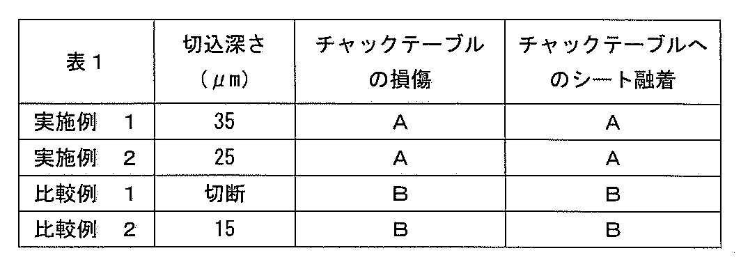
The same operation as in Example 1 was performed except that an ethylene-methacrylic acid copolymer film (methacrylic acid copolymerization ratio 9% by weight) having a thickness of 100 μm was used as the base film. The results are shown in Table 1.
実施例1および2のレーザーダイシングシートは、切断されることもなく、チャックテーブルの損傷およびチャックテーブルへの融着もみられなかった。比較例1のレーザーダイシングシートは、切断され、チャックテーブルの損傷およびチャックテーブルへの融着がみられた。比較例2のレーザーダイシングシートは、切断されることがなかったが、ダイシングシートを透過したレーザー光によりチャックテーブルの損傷およびチャックテーブルへの融着がみられた。 The laser dicing sheets of Examples 1 and 2 were not cut, and the damage to the chuck table and the fusion to the chuck table were not observed. The laser dicing sheet of Comparative Example 1 was cut and the chuck table was damaged and fused to the chuck table. The laser dicing sheet of Comparative Example 2 was not cut, but damage to the chuck table and fusion to the chuck table were observed by the laser light transmitted through the dicing sheet.
Claims (5)
レーザー光によりワークを個片化してチップを作製する、チップ体の製造方法。 Affixing a workpiece on the adhesive layer of the laser dicing sheet according to any one of claims 1 to 4,
A method for manufacturing a chip body, wherein a chip is manufactured by dividing a workpiece into pieces by laser light.
Priority Applications (1)
| Application Number | Priority Date | Filing Date | Title |
|---|---|---|---|
| JP2008047365A JP5225711B2 (en) | 2008-02-28 | 2008-02-28 | Laser dicing sheet and chip body manufacturing method |
Applications Claiming Priority (1)
| Application Number | Priority Date | Filing Date | Title |
|---|---|---|---|
| JP2008047365A JP5225711B2 (en) | 2008-02-28 | 2008-02-28 | Laser dicing sheet and chip body manufacturing method |
Publications (2)
| Publication Number | Publication Date |
|---|---|
| JP2009206311A JP2009206311A (en) | 2009-09-10 |
| JP5225711B2 true JP5225711B2 (en) | 2013-07-03 |
Family
ID=41148284
Family Applications (1)
| Application Number | Title | Priority Date | Filing Date |
|---|---|---|---|
| JP2008047365A Active JP5225711B2 (en) | 2008-02-28 | 2008-02-28 | Laser dicing sheet and chip body manufacturing method |
Country Status (1)
| Country | Link |
|---|---|
| JP (1) | JP5225711B2 (en) |
Families Citing this family (1)
| Publication number | Priority date | Publication date | Assignee | Title |
|---|---|---|---|---|
| JP6334223B2 (en) * | 2014-03-26 | 2018-05-30 | リンテック株式会社 | Adhesive sheet |
Family Cites Families (6)
| Publication number | Priority date | Publication date | Assignee | Title |
|---|---|---|---|---|
| JP3520996B2 (en) * | 1991-12-24 | 2004-04-19 | 三菱化学ポリエステルフィルム株式会社 | Adhesive sheet for attaching semiconductor wafers |
| JPH0687938A (en) * | 1992-09-07 | 1994-03-29 | Three Bond Co Ltd | Photo-setting resin composition |
| JPH11189762A (en) * | 1997-12-26 | 1999-07-13 | Nippon Kayaku Co Ltd | Resin composition for adhesive sheet substrate, substrate for adhesive sheet and adhesive sheet using the same |
| JP2001226649A (en) * | 2000-02-15 | 2001-08-21 | Hitachi Kasei Polymer Co Ltd | Water-peelable double-sided tape |
| JP4476848B2 (en) * | 2005-03-07 | 2010-06-09 | リンテック株式会社 | Laser dicing sheet and laser dicing method |
| JP4851246B2 (en) * | 2006-06-12 | 2012-01-11 | 古河電気工業株式会社 | A dicing tape for laser dicing based on a composition having a phase separation structure obtained by adding a hydrogenated styrene / butadiene copolymer to polypropylene. |
-
2008
- 2008-02-28 JP JP2008047365A patent/JP5225711B2/en active Active
Also Published As
| Publication number | Publication date |
|---|---|
| JP2009206311A (en) | 2009-09-10 |
Similar Documents
| Publication | Publication Date | Title |
|---|---|---|
| TWI680879B (en) | Mask-integrated surface protection tape and method for manufacturing semiconductor wafer using the same | |
| JP5059559B2 (en) | Laser dicing sheet and chip body manufacturing method | |
| JP6018730B2 (en) | Dicing sheet and semiconductor chip manufacturing method | |
| JP5367990B2 (en) | Laser dicing sheet and chip body manufacturing method | |
| JP2011139042A (en) | Adhesive sheet for stealth dicing and method of manufacturing semiconductor device | |
| TWI689000B (en) | Masking material for plasma cutting, mask-integrated surface protection tape and method for manufacturing semiconductor wafer | |
| EP2091073B1 (en) | Laser dicing using an adhesive sheet | |
| WO2013141251A1 (en) | Film, sheet substrate for processing workpiece, and sheet for processing workpiece | |
| JP5059558B2 (en) | Laser dicing sheet and chip body manufacturing method | |
| JP5314308B2 (en) | Laser dicing / die-bonding sheet and chip composite manufacturing method | |
| JP6334223B2 (en) | Adhesive sheet | |
| KR20180132620A (en) | Mask-integrated surface protection tape | |
| JP5149888B2 (en) | Stealth dicing adhesive sheet and method for manufacturing semiconductor device | |
| KR20170128210A (en) | Adhesive tape for semiconductor wafer processing | |
| US8114520B2 (en) | Laser dicing sheet and process for producing chip body | |
| JP5225710B2 (en) | Laser dicing sheet and chip body manufacturing method | |
| JP5009659B2 (en) | Dicing sheet and chip body manufacturing method | |
| JP5225711B2 (en) | Laser dicing sheet and chip body manufacturing method | |
| KR101883648B1 (en) | Film and adhesive sheet | |
| JP5314307B2 (en) | Laser dicing / die-bonding sheet and chip composite manufacturing method | |
| KR20000063979A (en) | adhesive composition curing by UV-light and adhesive sheet for manufacturing semiconductor wafer | |
| KR20200144090A (en) | Work sheet |
Legal Events
| Date | Code | Title | Description |
|---|---|---|---|
| A621 | Written request for application examination |
Free format text: JAPANESE INTERMEDIATE CODE: A621 Effective date: 20100830 |
|
| A977 | Report on retrieval |
Free format text: JAPANESE INTERMEDIATE CODE: A971007 Effective date: 20120613 |
|
| A131 | Notification of reasons for refusal |
Free format text: JAPANESE INTERMEDIATE CODE: A131 Effective date: 20120703 |
|
| RD02 | Notification of acceptance of power of attorney |
Free format text: JAPANESE INTERMEDIATE CODE: A7422 Effective date: 20120830 |
|
| TRDD | Decision of grant or rejection written | ||
| A01 | Written decision to grant a patent or to grant a registration (utility model) |
Free format text: JAPANESE INTERMEDIATE CODE: A01 Effective date: 20130305 |
|
| A61 | First payment of annual fees (during grant procedure) |
Free format text: JAPANESE INTERMEDIATE CODE: A61 Effective date: 20130313 |
|
| R150 | Certificate of patent or registration of utility model |
Ref document number: 5225711 Country of ref document: JP Free format text: JAPANESE INTERMEDIATE CODE: R150 Free format text: JAPANESE INTERMEDIATE CODE: R150 |
|
| FPAY | Renewal fee payment (event date is renewal date of database) |
Free format text: PAYMENT UNTIL: 20160322 Year of fee payment: 3 |
|
| R250 | Receipt of annual fees |
Free format text: JAPANESE INTERMEDIATE CODE: R250 |
|
| R250 | Receipt of annual fees |
Free format text: JAPANESE INTERMEDIATE CODE: R250 |
|
| R250 | Receipt of annual fees |
Free format text: JAPANESE INTERMEDIATE CODE: R250 |
|
| R250 | Receipt of annual fees |
Free format text: JAPANESE INTERMEDIATE CODE: R250 |
|
| R250 | Receipt of annual fees |
Free format text: JAPANESE INTERMEDIATE CODE: R250 |
|
| R250 | Receipt of annual fees |
Free format text: JAPANESE INTERMEDIATE CODE: R250 |
|
| R250 | Receipt of annual fees |
Free format text: JAPANESE INTERMEDIATE CODE: R250 |
|
| R250 | Receipt of annual fees |
Free format text: JAPANESE INTERMEDIATE CODE: R250 |
|
| R250 | Receipt of annual fees |
Free format text: JAPANESE INTERMEDIATE CODE: R250 |
|
| R250 | Receipt of annual fees |
Free format text: JAPANESE INTERMEDIATE CODE: R250 |
|
| R250 | Receipt of annual fees |
Free format text: JAPANESE INTERMEDIATE CODE: R250 |