JP5224014B2 - System and method for removing contaminant particles from an ion beam - Google Patents
System and method for removing contaminant particles from an ion beam Download PDFInfo
- Publication number
- JP5224014B2 JP5224014B2 JP2002524184A JP2002524184A JP5224014B2 JP 5224014 B2 JP5224014 B2 JP 5224014B2 JP 2002524184 A JP2002524184 A JP 2002524184A JP 2002524184 A JP2002524184 A JP 2002524184A JP 5224014 B2 JP5224014 B2 JP 5224014B2
- Authority
- JP
- Japan
- Prior art keywords
- ion beam
- particles
- electric field
- ion
- ions
- Prior art date
- Legal status (The legal status is an assumption and is not a legal conclusion. Google has not performed a legal analysis and makes no representation as to the accuracy of the status listed.)
- Expired - Lifetime
Links
Images


Classifications
-
- H—ELECTRICITY
- H01—ELECTRIC ELEMENTS
- H01J—ELECTRIC DISCHARGE TUBES OR DISCHARGE LAMPS
- H01J37/00—Discharge tubes with provision for introducing objects or material to be exposed to the discharge, e.g. for the purpose of examination or processing thereof
- H01J37/30—Electron-beam or ion-beam tubes for localised treatment of objects
-
- H—ELECTRICITY
- H01—ELECTRIC ELEMENTS
- H01J—ELECTRIC DISCHARGE TUBES OR DISCHARGE LAMPS
- H01J37/00—Discharge tubes with provision for introducing objects or material to be exposed to the discharge, e.g. for the purpose of examination or processing thereof
- H01J37/02—Details
- H01J37/026—Means for avoiding or neutralising unwanted electrical charges on tube components
-
- H—ELECTRICITY
- H01—ELECTRIC ELEMENTS
- H01J—ELECTRIC DISCHARGE TUBES OR DISCHARGE LAMPS
- H01J37/00—Discharge tubes with provision for introducing objects or material to be exposed to the discharge, e.g. for the purpose of examination or processing thereof
- H01J37/30—Electron-beam or ion-beam tubes for localised treatment of objects
- H01J37/3002—Details
-
- H—ELECTRICITY
- H01—ELECTRIC ELEMENTS
- H01J—ELECTRIC DISCHARGE TUBES OR DISCHARGE LAMPS
- H01J37/00—Discharge tubes with provision for introducing objects or material to be exposed to the discharge, e.g. for the purpose of examination or processing thereof
- H01J37/30—Electron-beam or ion-beam tubes for localised treatment of objects
- H01J37/317—Electron-beam or ion-beam tubes for localised treatment of objects for changing properties of the objects or for applying thin layers thereon, e.g. for ion implantation
- H01J37/3171—Electron-beam or ion-beam tubes for localised treatment of objects for changing properties of the objects or for applying thin layers thereon, e.g. for ion implantation for ion implantation
-
- H—ELECTRICITY
- H01—ELECTRIC ELEMENTS
- H01J—ELECTRIC DISCHARGE TUBES OR DISCHARGE LAMPS
- H01J2237/00—Discharge tubes exposing object to beam, e.g. for analysis treatment, etching, imaging
- H01J2237/004—Charge control of objects or beams
-
- H—ELECTRICITY
- H01—ELECTRIC ELEMENTS
- H01J—ELECTRIC DISCHARGE TUBES OR DISCHARGE LAMPS
- H01J2237/00—Discharge tubes exposing object to beam, e.g. for analysis treatment, etching, imaging
- H01J2237/02—Details
- H01J2237/022—Avoiding or removing foreign or contaminating particles, debris or deposits on sample or tube
-
- H—ELECTRICITY
- H01—ELECTRIC ELEMENTS
- H01J—ELECTRIC DISCHARGE TUBES OR DISCHARGE LAMPS
- H01J2237/00—Discharge tubes exposing object to beam, e.g. for analysis treatment, etching, imaging
- H01J2237/30—Electron or ion beam tubes for processing objects
- H01J2237/317—Processing objects on a microscale
- H01J2237/31701—Ion implantation
- H01J2237/31705—Impurity or contaminant control
Description
本発明は、一般にイオンビーム処理に関し、特にイオンビームに対する汚染粒子を取り除くためのシステムおよび方法に関する。 The present invention relates generally to ion beam processing, and more particularly to a system and method for removing contaminant particles from an ion beam.
半導体装置の製造において、イオン注入機は、半導体ウエハまたはガラス基板に不純物を添加するのに使用される。イオンビーム注入機は、不純物を添加してn型又はp型の半導体材料を製造したり又は集積回路の製造中に不活性層を形成するためにイオンビームでシリコンウエハを処理するのに使用される。イオンビ一ム注入機は、半導体に不純物を添加するのに用いられるとき、所望の半導体材料を製造するのに選択されたイオン種を注入する。アンチモンや砒素や燐等のイオン源材料から発生されぐ注入イオンは、結果的にn型の半導体材料のウエハを生むことになり、一方、p型の半導体材料のウエハが必要とされる場合、ボロンやガリウムやインジウム等のイオン源材料から生成されるイオンが注入される。 In the manufacture of semiconductor devices, ion implanters are used to add impurities to semiconductor wafers or glass substrates. Ion beam implanters are used to process silicon wafers with ion beams to add impurities to produce n-type or p-type semiconductor material or to form an inactive layer during integrated circuit fabrication. The An ion beam implanter, when used to add impurities to a semiconductor, injects selected ionic species to produce the desired semiconductor material. Implanted ions generated from an ion source material such as antimony, arsenic, or phosphorus result in a wafer of n-type semiconductor material, while a wafer of p-type semiconductor material is required, Ions generated from ion source materials such as boron, gallium, and indium are implanted.
一般的なイオンビーム注入機は、イオン化可能材料から正電荷イオンを発生させるためのイオン源を有している。生成されたイオンは、ビームに形成され、所定のビーム経路に沿って注入ステーションに導かれる。イオンビーム注入機は、イオン源と注入ステーションとの間に延びたビーム形成/整形構造体を有している。この構造体は、イオンビームを維持し、ビームが注入ステーションへの途上で通る細長い内部キャビティまたは通路の境界を定めている。イオン注入機を動作させるときには、この通路は、イオンがガス分子と衝突した結果として所定のビーム経路から偏向する確率が低下するように、一般的に排気されている。 A typical ion beam implanter has an ion source for generating positively charged ions from an ionizable material. The generated ions are formed into a beam and guided to an implantation station along a predetermined beam path. The ion beam implanter has a beam forming / shaping structure that extends between an ion source and an implantation station. This structure maintains the ion beam and delimits an elongated internal cavity or passage through which the beam passes on its way to the implantation station. When operating the ion implanter, this passage is generally evacuated so that the probability of ions deflecting from a predetermined beam path as a result of collisions with gas molecules is reduced.
イオンの電荷に対する質量(例えば、電荷対質量比)は、静電界や磁界によって軸方向と横断方向の両方にイオンが加速される度合に影響する。従って、望ましくない分子質量のイオンはビームから離れた位置に偏向され、所望の材料以外の注入が回避されるので、半導体ウエハの所望の領域や他のターゲットに到達するビームは非常に純度の高いものになる。望ましいまた望ましくない電荷対質量比のイオンを選択的に分離するプロセスは、質量分析として知られている。質量分析器は、一般的に、異なった電荷対質量比のイオンを効果的に分離するアーチ状通路において磁気偏向作用を介してイオンビームの種々のイオンを偏向させるために、双極子磁界をつくり出す質量分析磁石を用いている。 The mass of an ion relative to its charge (eg, charge-to-mass ratio) affects the degree to which the ion is accelerated in both the axial and transverse directions by an electrostatic or magnetic field. Thus, ions of undesirable molecular mass are deflected away from the beam, avoiding implantation other than the desired material, so that the beam reaching the desired area of the semiconductor wafer and other targets is very pure. Become a thing. The process of selectively separating desirable and undesired charge-to-mass ratio ions is known as mass spectrometry. Mass analyzers typically create a dipole magnetic field to deflect various ions of an ion beam via magnetic deflection action in an arcuate path that effectively separates ions of different charge to mass ratios. A mass analysis magnet is used.
イオンビームは、基板の所望表面領域に焦点を合わせかつ向けられている。一般的に、イオンビームの活性化イオンは、所定のエネルギーレベルに加速され、ワークピースの塊の中を貫通する。このイオンは、所望の導電率の領域を形成するために材料の結晶格子内に埋め込まれ、イオンビームエネルギーによりイオン注入の深さが決定する。イオン注入システムの例として役立つものは、マサチューセッツ、ベバリーにあるアクセリス テクノロジーズ社のものが含まれる。 The ion beam is focused and directed to the desired surface area of the substrate. In general, the activated ions of the ion beam are accelerated to a predetermined energy level and penetrate through the workpiece mass. The ions are embedded in the crystal lattice of the material to form a region of the desired conductivity, and the ion implantation depth determines the ion implantation depth. Useful examples of ion implantation systems include those from Axcelis Technologies, Inc. in Beverly, Massachusetts.
イオン注入機または他のイオンビーム装置(例えば、リニア加速器)の作動によって、汚染粒子が生産されることになる。この汚染粒子は、例えば、約1μm以下の大きさである。粒子に衝突するイオンビーム内のイオンの運動量により、粒子は、イオンビームとともに移動されるが、一般的に、イオンよりもその速度はかなり遅い。その結果、イオンビーム内に伴出される粒子は、ウエハ(または他の基板)の方にイオンビームの流れに伴って運ばれ、その結果、ウエハにおいて、望ましくない汚染が生じる。 Operation of an ion implanter or other ion beam device (eg, a linear accelerator) will produce contaminating particles. For example, the contamination particles have a size of about 1 μm or less. Due to the momentum of the ions in the ion beam impinging on the particles, the particles are moved with the ion beam, but generally at a much slower rate than the ions. As a result, particles entrained in the ion beam are carried with the ion beam flow toward the wafer (or other substrate), resulting in undesirable contamination in the wafer.
イオン注入システムにおいて、例えば、1つの汚染粒子源は、フォトレジスト材料である。フォトレジスト材料は、注入する前にウエハ表面に被膜され、そして、完成した集積回路の回路構成を規定するのに用いられる。イオンがウエハ表面に衝突するとき、フォトレジスト被膜の粒子は、ウエハから除去され、イオンビームの流れによって運ばれる。イオン注入中に半導体ウエハ又は他の基板に衝突および固着する汚染粒子は、処理されたウエハの超顕微鏡的なパターンの精密度を必要とする半導体及び他の素子の製造における製造損失の一因となる。 In an ion implantation system, for example, one contaminant particle source is a photoresist material. The photoresist material is coated on the wafer surface prior to implantation and is used to define the circuit configuration of the completed integrated circuit. As the ions strike the wafer surface, the photoresist coating particles are removed from the wafer and carried by the ion beam stream. Contaminating particles that impact and adhere to the semiconductor wafer or other substrate during ion implantation contribute to manufacturing losses in the manufacture of semiconductors and other devices that require precision in the microscopic pattern of the processed wafer. Become.
半導体素子は、寸法を縮小して、より精密に製造されるので、より高度な正確さと効率を備える装置が、このような半導体素子を製造するために必要とされる。従って、ウエハの汚染を軽減するために、イオンビーム内の汚染粒子レベルを減少させることが望ましい。
(発明の開示)Since semiconductor devices are manufactured more precisely with reduced dimensions, an apparatus with a higher degree of accuracy and efficiency is required to manufacture such semiconductor devices. Therefore, it is desirable to reduce the level of contaminating particles in the ion beam to reduce wafer contamination.
(Disclosure of the Invention)
【課題を解決するための手段】
本発明の1つは、イオンビームに対する汚染粒子を容易に取り除くためのシステムおよび方法に関する。イオンビームは、イオンビームの粒子と異なる極性に荷電された粒子が存在する領域の中を移動する。この粒子が荷電される場所よりも下流に電界を発生して、この電界によってイオンビームの流れとともに移動する汚染粒子をイオンビーム流れから離れる方向に向かわせるようにする。電界はまた、イオンビームを所望レベルに加速するための加速領域を与える。その結果、本発明によれば、粒子は、イオンビームの移動方向から離れる、即ち、取り除くことができる。これにより、ワークピースの汚染を軽減する。
[Means for Solving the Problems]
One aspect of the present invention relates to a system and method for easily removing contaminant particles from an ion beam. The ion beam travels in a region where particles charged with a polarity different from that of the ion beam particles are present. An electric field is generated downstream from where the particles are charged, and this electric field causes the contaminating particles moving with the ion beam flow to be directed away from the ion beam flow. The electric field also provides an acceleration region for accelerating the ion beam to a desired level. As a result, according to the present invention, the particles can be moved away from the direction of movement of the ion beam, ie removed. This reduces the contamination of the workpiece.
本発明の他の形態では、イオンビームの流れと共に粒子が移動するのを抑止するためのシステムを提供する。このシステムは、イオンビームの粒子と異なる極性に粒子を荷電するための粒子荷電システムを含む。1つの電界発生器が、この粒子荷電システムよりも下流に電界を発生し、イオンビーム内に配置された荷電粒子をイオンビームの移動方向から離れるようにする。 In another aspect of the invention, a system is provided for inhibiting the movement of particles with the ion beam flow. The system includes a particle charging system for charging particles to a different polarity than the particles of the ion beam. One electric field generator generates an electric field downstream from the particle charging system, and causes charged particles disposed in the ion beam to move away from the moving direction of the ion beam.
また、本発明の別の形態では、イオンビームと共に粒子が移動するのを抑止するためのシステムを提供する。このシステムは、一般的にイオンビームを取り囲むプラズマ領域内にプラズマを注入するためのプラズマ発生器を含む。また、電界発生器は、イオンビームの移動方向にほぼ平行な電界を発生しかつプラズマ領域に対して下流に配置されている。プラズマ領域内に配置された粒子は負に荷電され、電界によって、イオンビーム内に配置された負電荷の粒子をイオンビームの移動方向から離れるように強制する。 In another aspect of the present invention, a system is provided for inhibiting particles from moving with the ion beam. The system generally includes a plasma generator for injecting a plasma into a plasma region surrounding the ion beam. The electric field generator generates an electric field substantially parallel to the moving direction of the ion beam and is disposed downstream of the plasma region. Particles placed in the plasma region are negatively charged and the electric field forces the negatively charged particles placed in the ion beam away from the direction of ion beam movement.
本発明の別の形態では、イオン注入システムを提供する。このシステムは、注入ステーションに配置された基板を処理するためにイオンを注入するイオン源と、注入軌道に所望の質量のイオンを偏向させるための質量分析磁石システムとを含む。粒子除去システムは、分析磁石シヌテムから偏向したイオンと共に汚染粒子が移動するのを抑止する。この粒子除去システムは、偏向したイオンと異なる極性に粒子を荷電するための粒子荷電システムを含む。1つの電界がこの粒子荷電システムよりも下流に発生する。この電界は、少なくとも一部の荷電粒子を偏向したイオンの移動方向から離すように作動する。基板が注入ステーションに支持されており、このステーションにおいて、粒子除去システムからのイオンが処理される。これにより、基板での粒子の汚染が軽減される。 In another aspect of the invention, an ion implantation system is provided. The system includes an ion source that implants ions to process a substrate located at an implantation station, and a mass analysis magnet system for deflecting ions of a desired mass into the implantation trajectory. The particle removal system deters migration of contaminating particles along with ions deflected from the analysis magnet synutem. The particle removal system includes a particle charging system for charging particles to a polarity different from that of deflected ions. One electric field is generated downstream from the particle charging system. This electric field operates to move at least some charged particles away from the direction of movement of the deflected ions. The substrate is supported by an implantation station where ions from the particle removal system are processed. This reduces particle contamination on the substrate.
更に本発明の別の形態では、イオンビームと共に粒子が移動するのを抑止する方法を提供する。この方法は、イオンビームの極性と異なる極性に粒子を荷電させ、そして、粒子が荷電される領域よりも下流に電界を発生させることを含んでいる。少なくとも一部の荷電粒子は、イオンビームの移動方向から離れるように強制される。 Yet another aspect of the present invention provides a method for inhibiting the movement of particles with an ion beam. This method involves charging the particles to a polarity different from the polarity of the ion beam and generating an electric field downstream of the region where the particles are charged. At least some charged particles are forced away from the direction of ion beam movement.
本発明の別の構成は、イオンビームと共に粒子を移動するのを抑止する方法を提供する。この方法は、イオンビームが負の荷電粒子に対して移動する領域内に電子を放出することを含む。イオンビームの移動方向から荷電粒子が強制的に離れるように、電界が発生する。 Another configuration of the present invention provides a method for inhibiting movement of particles with an ion beam. The method includes emitting electrons into a region where the ion beam moves relative to negatively charged particles. An electric field is generated so that the charged particles are forcibly separated from the moving direction of the ion beam.
上述の及びこれに関連する目的を達成するために、以下の詳細な説明とこれに付随する図面によって、本発明の例示的構成が記載されている。しかし、これらの形態は、例示的なものであり、本発明の原理のために使用する種々の方法のいくつかに過ぎない。そして、本発明は、このような全ての構成および等価物を含むことを意図している。本発明の他の利点及び新規な特徴は、図面との関連で考えると本発明についての以下の詳細な説明から明らかになる。 To the accomplishment of the foregoing and related ends, illustrative configurations of the invention are described by the following detailed description and accompanying drawings. However, these forms are exemplary and are only some of the various methods used for the principles of the present invention. The present invention is intended to include all such configurations and equivalents. Other advantages and novel features of the invention will become apparent from the following detailed description of the invention when considered in conjunction with the drawings.
図1は、本発明に従う粒子除去システムの側部断面図である。図2は、本発明に従う粒子軌道の一例を示す図1のシステムにおける別の断面図である。図3は、本発明に従う粒子除去システムを用いるイオン注入システムの概略的なブロック図である。図4は、本発明に従う粒子除去システムを用いるイオン注入システムの一例を示す部分断面図である。図5は、本発明に従うイオンビームと共に粒子が移送されるのを抑止する方法を示すフローチャート図である。 FIG. 1 is a side cross-sectional view of a particle removal system according to the present invention. FIG. 2 is another cross-sectional view of the system of FIG. 1 showing an example of a particle trajectory according to the present invention. FIG. 3 is a schematic block diagram of an ion implantation system using a particle removal system according to the present invention. FIG. 4 is a partial cross-sectional view showing an example of an ion implantation system using the particle removal system according to the present invention. FIG. 5 is a flow chart diagram illustrating a method for inhibiting the transfer of particles with an ion beam according to the present invention.
本発明は、イオンビームに対する汚染粒子を取り除くために、イオン注入システムに関連して使用されるシステム及び方法を提供する。しかし、本発明は、イオン注入機と共に用いるばかりでなく広範囲の応用を有していることが理解できるであろう。本発明は、ここに記載された以外の利用において、イオンビームから汚染粒子を取り除くのに役立つように使用することができる。さらに、図1〜図5に関して図示されかつ記載された実施形態は、正のイオンビームから粒子を取り除くことを主として開示しているが、当業者であれば、本発明は、負のイオンビームから粒子を取り除く場合にも等しく利用できることが理解できかつ明らかになるであろう。 The present invention provides a system and method used in conjunction with an ion implantation system to remove contaminant particles for an ion beam. However, it will be appreciated that the present invention has a wide range of applications as well as being used with ion implanters. The present invention can be used to help remove contaminant particles from an ion beam in applications other than those described herein. Furthermore, although the embodiments illustrated and described with respect to FIGS. 1-5 primarily disclose removing particles from a positive ion beam, those skilled in the art will recognize that the present invention can be applied to a negative ion beam. It will be understood and apparent that it can be used equally well when removing particles.
図1は、本発明の構成に従う粒子除去システム10を示している。このシステム10は、イオンビーム16が移動するプラズマシース14を形成するために、電子を放出するプラズマ発生器12を含んでいる。イオンビーム16は、ビーム軸線Aを有し、参照符号18で示すビーム方向に下流へと流れる。イオンビーム16は、例えば、正の電界を生じる正の荷電粒子から形成される。その結果、イオンビーム16とプラズマシース14との間に境界が形成され、このプラズマシースは、イオンビームをほぼ取り囲む。プラズマシース14は、汚染粒子を生じる環境を与えて、イオンビームの外側に配置されるプラズマ領域において、プラズマの極性に一致する負電荷を蓄積する。 FIG. 1 shows a
例えば、プラズマ発生器12は、プラズマ電子ブラッド(PEF)システムとして構成することが可能である。このPEFシステムは、ハウジング内に配置された導電性コイル22から電気的に絶縁された導電性ハウジング20を含んでいる。このコイル22は、タングステンまたは他の適切な材料から形成することができ、コイルからハウジング20にアークを発生させるのに十分な電位にコイルが励磁される。例えば、コイル22は、ハウジング20の電位に対して約40kV高くなるように励磁される。適当な材料によるガス源は、ガスをハウジング内に注入するためにハウジング20に連結されている。ガス源24は、ハウジング20の上端部に連結されるように概略的に図示されているが、当業者であれば、ハウジングの内部と流体連通する適当な導管を介してハウジング20の側壁内にガスが放出されうることが理解できるであろう。 For example, the
コイル22とハウジング20の間に発生したアークによって、電子を活性化させる(即ち、ガス源24によって与えられるガスの分子から電子を取り除く。)。その結果、ハウジング20は、放出されたガス状媒体、すなわちプラズマの電子で満たされる。開口28は、ハウジング20を貫通しており、発生したプラズマがハウジングの内部領域から開口26へ、イオンビーム16の経路に対してほぼ垂直な方向に流れる。この注入されたプラズマは、次に負に荷電された高密度のプラズマシース14を形成する。
The arc generated between the
図1で示すように、プラズマ発生器は、電気導電性の終端電極32の、ほぼ円筒状の側壁30に取り付けられている。電気絶縁材料のスペーサ34は、ハウジング20と終端電極32の間に介装されており、ハウジングを電極から電気的に分離する。終端電極32の側壁30は、ビーム軸線Aに対してほぼ同軸にある。終端電極32は、上流端に入口開口36を有し、この開口を通ってイオンビーム16が終端電極の内部領域に入る。また、終端電極32は、電気導電性の環状プレートを有し、この環状プレートは、終端電極の下流端に取り付けられている。環状プレート38は、出口開口40を有し、この出口開口を介してイオンビーム16が終端電極から排出される。 As shown in FIG. 1, the plasma generator is attached to a substantially
終端電極32は、電源42に電気的に接続され、電源は、終端電極を接地電位44に対して正電圧の電位に印加する。また、コイル22が終端電極32に接続され、一方ハウジング20が接地電位44に接続することができる。このような場合、コイル22と終端電極32は、共に同一電位になっている。 The
プラズマシース14は、終端電極32の内部領域を満たし、イオンビーム16を取り囲む。終端電極32の内部領域内に電子を高密度に維持するのを促進するために、1つまたはそれ以上の永久磁石48を終端電極の内側表面に沿って配置することができる。この磁石48は、終端電極の内側表面に沿って電界を形成し、終端電極の内壁に対して電子を軽減するように制御する。これにより、終端電極内のプラズマ密度が増加する。プラズマシース14は、有利なことに、終端電極領域においてイオンビーム16によって生じる空間電荷を中和する傾向を有する。これにより、ビーム安定性が改善される。 The plasma sheath 14 fills the inner region of the
電界50は、終端電極32に対して下流に発生し、負の荷電粒子及びプラズマ14がビームの移動方向18から遠ざかるように強制される。この例では、電極52は、終端電極32に対して下流に配置された可変分解電極となり、この電極52は電界50を発生する。電極52は、開口54(変更可能な分解開口)を含み、この開口を介してイオンビームが通過する。電源56は、電気的に電極52に接続されて、終端電極32に対して低い電位にある電極を形成する。特に、終端電極32の下流端に電気的に接続される環状プレート38は、加速システムを形成するために電極52に接続した1つの電極として作動する。この加速システム59は、電界50の強さ及び方向に従って所望のレベルになるまでイオンビーム16内で移動するイオンを加速する。例えば、ビーム軸にほぼ平行に電界を向かわせるように、プレート38と電極52は、共にビーム軸Aにほぼ垂直に配置される。また、電極52は、イオンビーム16内のイオンを加速するための大きな加速間隙58を与えるように、電極38の電圧に対して約−40KVの電圧を有する電位にすることができる。
The
また、電界50は、プラズマと電界の間の境界60を形成するように作動する。特に、電界50は、ビーム軌道18の方向と反対の方向(62で示す)に、電子及び負に荷電された粒子に力を作用させる。その結果、電界50は、これらの粒子が出口開口40(即ち、プラズマシース14を無効にする電界)を通ってプラズマシース14への下流へ移動するのを抑止する。この電界は、また、イオンビーム16内のイオンに下流方向への力を作用させ、複数のイオンを加速する。 The
境界60では、プラズマ14と関連する電界に対する電界50の強さに応じて急激に変化する。プラズマ密度および/または電界の強さを増加させることにより、より急激な、即ち、鋭い境界を形成することができる。鋭いプラズマ境界60は、次に汚染粒子を反発させてビーム軌道18の方向から遠ざける能力を改善する。イオンビームにおいて、プラズマ14が欠乏すると、正に荷電された汚染粒子を有する環境を作り出すが、このプラズマによって負に荷電された粒子は、境界60に到達する前に正電荷を蓄積することができない。従って、通常、これらの粒子が境界60に到達するとき、粒子は、負に荷電されたままに残る。その結果、電界50は、負に荷電された粒子を反発して、ビーム移動方向18から外側に遠ざける。 At the
理解できるように、他のシステム(別システムおよび/または付加システム)を使用して、本発明の構成に従って、汚染粒子をビーム方向から遠ざけるように強制して下流の電界に対して上流に所望の荷電領域を設けることができる。例として、電子シャワーまたは、マイクロ波電力を導くためのシステムは、加速ギャップ58に進む前に粒子を負電荷に変化させるために使用することができる。さらに、負のイオンビームに対して適当な機構を用いることができ、本発明の構成によれば、粒子を正電荷に帯電させ、そして、適当な電界を下流に形成して、粒子を偏向しかつイオンビームを加速することができることは、当業者であれば理解できるであろう。 As can be appreciated, other systems (separate and / or additional systems) can be used to force contaminant particles away from the beam direction in accordance with the configuration of the present invention, as desired upstream relative to the downstream electric field. A charged region can be provided. As an example, an electronic shower or system for directing microwave power can be used to change the particles to a negative charge before proceeding to the
図2は、図1のシステム10における粒子66の軌道を一例として示している。この図において、同一の参照符号は、図1に関して特定された同一の要素を表す。粒子は、一般的に、イオンビームのイオンより遅い大きさを有する粒子の速度でイオンビーム16内を移動する。その結果、イオンビーム16と共に移動する粒子の動きは、少なくとも一部分では、イオンビームのイオンから粒子66及び粒子自体の運動エネルギーに運動量を伝達するために正当化される。 FIG. 2 shows as an example the trajectory of
例として、粒子66は、イオンビーム16の外側のプラズマシース14内に位置する軌道から始まる。高密度のプラズマシース14において、イオンビーム16内のイオンより早い速度で多数の自由電子が移動し、そのため、粒子66は、電子に対して高い衝突率を有することになる。その結果、粒子66は、プラズマシース14内にいる間にかなり多くめ負電荷を蓄積する。粒子66’の運動エネルギーにより、この粒子は、イオンビーム内に運ばれ、そして、イオンの運動量により、粒子66’を境界60に向かってイオンビームの方向18に向かわせる。 As an example, the
粒子66”がイオンビーム16(プラズマフリーの状態にある)内に入ると、イオンビーム16のイオンは、この粒子と衝突するようになる。イオンビーム16内のプラズマ14が欠乏する環境が作り出されると、イオンは正に荷電された粒子となるので、この粒子が、境界60に到達する前に正に荷電されてしまう見込みはなくなる。これは、粒子は、プラズマシース14内に配置されている間、多くは負電荷を蓄積することになるからである。こうして、粒子66”は、通常、境界60に到達する前にほぼ負電荷の状態を維持する(プラズマシース内に存在するよりもイオンビーム内の方が負に帯電することが少ないが)。 As the
図2の例で説明するように、粒子66”は、ビーム軌道の方向から離れてイオンビーム16の外側に移動する。特に、電界50は、粒子66”に対して矢印62の方向に力を作用させる。そのため、本発明の形態によれば、粒子はイオンビーム16の外側に偏向する。イオンビーム16は、ビーム軌道18の方向にイオンを移動させる電界50を用いて境界を通過することができ、これにより、電界の強さに関連して所定量だけイオンビームを加速する。 As illustrated in the example of FIG. 2, the
図2に対して図示された上記構造に関して、本発明は、イオンビーム16からの汚染粒子を取り除くことができるシステム100を提供するものであることが理解できる。このシステムは、イオンビーム16の回りに形成される領域を使用して、イオンビームの極性とは異なる極性を有する電荷に汚染粒子66を荷電させる。この汚染粒子66は、この粒子自体の運動エネルギーを介して、イオンビーム16からプラズマシース14内に移動する。汚染粒子66は、プラズマシース14内に位置している間、対応した電荷を蓄積し、そして、磁石46または別の構造体のいずれかと衝突することに応じてイオンビーム46内に進入することができる。イオンビーム16内のイオンは、粒子と衝突し、これらの粒子を境界60の方に移動する。電界50は、イオンビーム軌道18の方向から粒子をそらすように作用する。これにより、イオンビームから汚染粒子を取り除くのを促進させる。さらに、粒子66が境界を通過して下流に移動する場合、粒子は、下流のワークピースまたは基板に衝突しないように、ビームの軌道方向から離れるように強制される。 With respect to the above structure illustrated with respect to FIG. 2, it can be seen that the present invention provides a
本発明の状況を与えるために、図3は、本発明に従う粒子除去システム102を用いるイオンビーム処理システム100を表す機能ブロック図である。例として、システム100は、イオン注入システム、粒子加速器、または(正または負の)イオンビームを使用する他のシステムとすることができ、このシステムにおいて、汚染粒子をビーム軌道の方向から離れるように偏向および/または除去することが望ましい。 To provide the context of the present invention, FIG. 3 is a functional block diagram representing an ion
このシステム100は、イオンビーム106を形成するイオンを放出するイオン源104を含む。イオン源104は、例えば、イオン化可能ガス又は気化した材料等のイオン源材料が放出されるチャンバを有する。イオンを発生するためにイオン源材料にエネルギーが加えられ、そして、チャンバから放出される(正または負の)イオンビーム106を形成する。イオン源は、当業者に良く知られており、その構成の詳細は、簡略化のために省略する。イオン源材料をイオン化するためにマイクロ波エネルギーを用いるイオン源の例は、米国特許第5,523652号明細書に開示されている。当業者であれば、本発明の構成に従う粒子除去システムは、付加的な処理を必要とする場合またはしない場合にも、イオン源の他の形式と連結して使用することができる。 The
本発明の形態に従って、イオン源104は、イオンビーム106を粒子除去システム102に供給する。粒子除去システム102は、イオンビームの極性とは異なる極性に粒子を荷電するための領域を用いる。この粒子を荷電する領域108は、電界110の下流に接続されて作動し、イオンビーム106内に伴出する汚染粒子の除去を容易にする。特に、電界110は、ビーム軌道の方向から汚染粒子が離れるように強制するために荷電された粒子に力を作用させるとともに、ビーム軌道の方向にイオンを加速するためにイオンビーム内のイオンに力(反対方向)を作用させる。 In accordance with an aspect of the present invention,
例として、粒子荷電領域108は、高密度のプラズマを含み、イオンビームが通過するガス状媒体内に多くの電子を有する。このプラズマは、公知のプラズマ発生システムによって発生する。電子を放出すること、又は粒子荷電領域内のプラズマ密度を増加させることは、粒子の荷電を高めるために利用することができる。プラズマは、ビーム方向にほぼ垂直の方向に供給される。 As an example, the particle charged
下流の電界110は、プラズマシースを無くして(または吹き消し)、粒子荷電領域と電界領域との間に境界(または障壁)を形成する。電界110は、例えば、ビーム軌道の方向に対してほぼ平行な方向に発生し、イオンビームを所望のレベルに加速する。電界110は、また、プラズマ内の負に荷電した粒子と電子に作用して、これらをビーム軌道の方向から離れるように強制する。負の粒子が多くなればなるほど、電界の強さが大きくなり、および/またはイオンビーム106に対する粒子の偏向が大きくなる。その結果、イオンビームが粒子除去システム102から出るとき、境界は、汚染粒子が加速されたイオンビーム106’と共に移送されるのを抑止する。 The downstream
粒子除去システム102は、イオンビーム106’を処理ステーション112に供給する。例として、処理ステーション112は、(イオン注入のための)イオン注入ステーション、(基板分析用の)分析ステーション、又はイオンビームを使用する他のシステムとすることができる。 The
コントローラ120は、イオン源104、粒子除去システム102、および処理ステーション112の各々と連結して作動する。このコントローラ120は、処理ステーション112に供給されるイオンビーム特性を監視しかつ制御する。コントローラ120は、イオンビーム106のパラメータを制御するために、システム100の種々の部品に対して機能的に所望の制御が実行できるようにソフトウエア及びハードウエアによりプログラムされおよび/または形作ることができる。 The
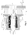
本発明のために更なる構成を与えるために、図4は、本発明の形態に従って粒子除去システム202を使用できるように形成したイオン注入システム200の例を示している。このイオン注入システム200は、イオン源210、質量分析磁石212、ビームラインアセンブリ214、及びターゲット即ちエンドステーション216を含んでいる。ビームラインアセンブリ214に対してエンドステーション216を動かすことができる、伸縮可能なステンレス鋼のベローズアセンブリ218が、エンドステーション216とビームラインアセンブリ214に連結されている。図4は、超低エネルギー(ULE)型イオン注入ステーションの例を図示しているが、本発明に従う粒子除去システムには、他の形式のイオン注入機にも同様に適用することができる。 In order to provide further configuration for the present invention, FIG. 4 shows an example of an
イオン源210は、プラズマ室220とイオン引き出しアセンブリ222を含んでいる。エネルギーがイオン化可能なドーパントガスに与えられて、プラズマ室220からイオンが発生する。一般的に、本発明は、負のイオンがイオン源210から発生するシステムに利用することもできるが、ここでは、正のイオンが発生する。正のイオンは、複数の電極から構成されるイオン引き出しアセンブリ222によって、プラズマ室220に設けたスリットを介して引き出される。電極224は、負電位の電圧にチャージされ、プラズマ室のスリットからの距離が増大すればするほど、電位が高くなる。従って、イオン引き出しアセンブリ222は、プラズマ室220から正のイオンのビーム228を引き出すように機能し、さらに、引き出されたイオンを質量分析磁石212内で加速する。 The
質量分析磁石212は、分解磁石ハウジング229及びビーム中和器230を含むビームラインアセンブリ214に対して適当な電荷対質量比を有するイオンを通過させる機能を有する。質量分析磁石212は、アーチ状の円筒側壁を有するアルミニウム製のビームガイド234によって形成される湾曲したビーム経路232を有する。このビーム経路は、真空ポンプ238によって排気される。この経路232に沿って伝搬するイオンビーム228は、質量分析磁石212によって発生する磁界に影響され、不適当な電荷対質量比のイオンを排除する。この双極子磁界の強さおよび方向は、磁石コネクタ246を介して磁石212の界磁巻線を通る電流を調整する制御用電子機器244によって制御される。 The
双極子磁界によって、イオンビーム228は、イオン源210に近い第1の、即ち、入口軌道247から分解ハウジング229に近い第2の、即ち、出口軌道248への湾曲したビーム経路232に沿って移動する。イオンビーム228の(不適当な電荷対質量比を有するイオンから構成される)部分228’、228”は、湾曲した軌道から離れて、アルミニウム製ビームガイド234の壁内へと偏向する。この例では、磁石212を通って分解ハウジング229内を通過するビーム228内のイオンは、所望の電荷対質量比を有している。 The dipole magnetic field causes the
例として、粒子除去システム202は、分解ハウジング229内に配置されているが、本発明に従って、このシステムは、イオン注入システム200の他の部品内に配置することも可能であることは理解できよう。例えば、粒子除去システム202は、ビームガイド234の下流端に配置することもできる。 By way of example, the
粒子除去システム202は、イオンビーム228から汚染粒子を離すように強制するための電界を発生する下流側の電界発生器252に接続される粒子荷電領域250を与えることにより汚染粒子の除去を容易にする。図4に示す粒子除去システム202は、図1に示されかつ記載されたものとほぼ同一のものとすることができる。簡単に言えば、粒子荷電領域250は、伸長しかつ略円筒形状の終端電極256の側壁に取り付けられたプラズマ発生器254を含んでいる。プラズマ発生器254は、プラズマシースを形成するプラズマ(プラズマは、イオンビームを終端電極256の内部領域内に取り囲む)を発生し、このプラズマシースを介してイオンビーム228が移動する。 The
電界は、終端電極256と下流の電極260との間に発生して、ビーム軌道の方向に対してほぼ平行な方向に指向する。プラズマシース内に配置された粒子は、イオンビーム228の極性(例えば、正の)とは異なる極性(例えば、負の)を有する電荷を蓄積する。電界は、荷電された粒子をビーム軌道の方向から離れるように強制する力を作用させる。イオンビーム228内のイオンは、粒子に対して反対の極性を有しているので、電界は、イオンに対して、荷電された粒子に作用する方向とは逆の方向に力を作用し、ビーム軌道の方向にイオンを加速させる。その結果、粒子除去システム202は、二重の機能を有し、汚染粒子をビーム軌道の方向から離れるように強制するとともに、イオンビーム228を加速する。 An electric field is generated between the termination electrode 256 and the
ビーム中和器230は、プラズマ中和シャワー266を有し、この中和シャワーは、正に荷電されたイオンビーム240によって注入される結果として、目標ウエハ上に蓄積する正の電荷を中和する。ビーム中和器230と分解ハウジング229は、真空ポンプ268によって排気されている。当業者には理解できるように、別個のビーム中和器230は、本発明の構成によれば、粒子除去システム202内のプラズマシースによって与えられる空間電荷の中和化のために必要としなくてもよい。
Beam neutralizer 230 includes a
ビーム中和器230の下流には、エンドステーション216があり、このエンドステーションは、ディスク形状のウエハ支持体270を含み、この上に、処理されるべきウエハが取り付けられる。ウエハ支持体270は、注入されるビームの方向に対してほぼ垂直なターゲット平面上に置かれる。モータ272は、ディスク形状のウエハ支持体270をエンドステーション216において回転させる。こうして、ウエハが円形経路内で移動するとき、ウエハ支持体に取り付けられたウエハにイオンビームが衝突する。エンドステーション216は、イオンビームの経路276とウエハWとの交点274の回りを旋回し、それゆえ、ターゲット平面は、この点の回りで調整可能である。 Downstream of the
図5は、本発明の形態に従うイオンビーム内において粒子の移送を抑止するための原理体系の一例を示すフローチャート図である。説明を簡単にするために、図5の原理体系は、一連のステップとして示されかつ記載されており、本発明は、これらのステップの順序に制限されるものではなく、いくつかのステップは、個々に示されかつ記載された他のステップを用いて並列してあるいは異なる順序で行うことができることは理解できよう。さらに、図示されたステップでない場合も、本発明の形態に従う原理体系を満たすために必要とされることもあり得る。 FIG. 5 is a flowchart showing an example of a principle system for suppressing the transfer of particles in the ion beam according to the embodiment of the present invention. For ease of explanation, the principle scheme of FIG. 5 is shown and described as a series of steps, and the present invention is not limited to the order of these steps, It will be appreciated that other steps shown and described individually can be used in parallel or in a different order. Further, even if it is not the illustrated step, it may be required to satisfy the principle system according to the embodiment of the present invention.
図5において、図示された原理体系では、ステップ310から始まる。このステップにおいて、イオンビームが供給される。このイオンビームは、正または負のイオンビームとすることができる。簡略化のために、以下の原理体系は、正のイオンビームに関して記述される。 In FIG. 5, the illustrated principle system starts at
ステップ320において、汚染粒子は、負に荷電される(イオンビームとは反対の極性)。例として、チャージングは、高密度のプラズマシースにおいて、電子と衝突することにより起こり、このプラズマシースは、ここで記載するように、イオンビームを取り囲む領域に配置される。電子シャワーを発生するためのシステム又はマイクロ波出力システム等により、負の電子は、汚染粒子を荷電するために与えられることは理解できよう。ステップ320から、処理はステップ330に進む。 In
ステップ330では、粒子が荷電される場所に対して下流に、電界が発生する。この電界は、イオンビームの経路に対してほぼ平行な方向に発生する。負に荷電されたプラズマシースと電界との間に境界が形成される。電界は、ビーム軌道の方向に対してほぼ反対方向にプラズマ上で作用する。荷電された汚染粒子がイオンビーム内に入ると、イオンビームの運動量によって、汚染粒子をプラズマ境界に向けて運ぶ。電界は、(プラズマ上で作用する粒子と同様の)荷電された粒子に作用して、これらの粒子をビーム軌道の方向から離すように強制する(ステップ340)。電界は、また、イオンビーム内のイオンに作用して、,これらのイオンをビーム軌道の方向に加速する(ステップ350)。 In
本発明を或る実施形態に関して図示しかつ説明してきたが、この明細書と添付された図面とを読んで理解すると他の当業者にも同等の変更や修正が行われるものと理解されよう。特に上述の構成要素(アセンブリ、装置、回路、システム等)によって実行される種々の機能に関して、そのような構成要素を説明するのに使用される用語(「手段」に対する参照を含めて)は、他に表示されていなければ、たとえ開示された構成に構造的に同等でなくても本発明のここで図示された例示的実施においてその機能を果たせば、説明された構成要素の特定された機能を実行する(即ち、機能的に同等である)いずれかの構成要素に相当するものと意図されている。これに関して、本発明は、種々の方向におけるステップを実行するために、コンピュータで実行可能な命令を有するコンピュータで読取可能な媒体を含んでいることも理解できよう。 While the invention has been illustrated and described with respect to certain embodiments, it will be understood that other changes and modifications will occur to others skilled in the art upon reading and understanding this specification and the accompanying drawings. The terms (including a reference to “means”) used to describe such components, particularly with respect to the various functions performed by the components described above (assemblies, devices, circuits, systems, etc.) are: Unless otherwise indicated, the specified function of the described component, if performed in the illustrated example implementation of the present invention, even if not structurally equivalent to the disclosed structure Is intended to correspond to any component that performs (ie, is functionally equivalent). In this regard, it will also be appreciated that the present invention includes a computer-readable medium having computer-executable instructions for performing steps in various directions.
更に、本発明の特定の特徴が幾つかの実施の内のただ一つに対して開示されてきたが、そのような特徴は、いずれかの或る又は特定の用途にとって望ましくかつ有利な他の実施形態における一つ以上の特徴と組み合わされ得るものである。更に、「含む」、「含んでいる」、「有する」、「有している」及びそれらの変形が詳細な説明か特許請求の範囲のいずれかで使用されている限り、これらの用語は、用語の『構成されている』と同様に内包的であると理解すべきである。 Moreover, while specific features of the invention have been disclosed for only one of several implementations, such features may be desirable and advantageous for any certain or specific application. It may be combined with one or more features in the embodiments. Further, as long as "include", "include", "have", "have" and variations thereof are used in either the detailed description or the claims, these terms It should be understood to be inclusive as well as the term “composed”.
(産業上の適用性)
本発明のシステム及び方法は、イオンビームに対して汚染粒子を取り除くためのシステム及び方法を提供するためのイオンビーム処理の分野に用いることができる。(Industrial applicability)
The system and method of the present invention can be used in the field of ion beam processing to provide a system and method for removing contaminant particles from an ion beam.
Claims (8)
イオンビーム(16)の極性と異なる極性に前記粒子を荷電するための粒子荷電システム(12)と、
この粒子荷電システム(12)に対して下流に電界(50)を発生して、この電界(50)がイオンビーム(16)内に置かれた荷電粒子を前記イオンビーム(16)の移動方向(18)から離れるように作動させる電界発生器(52)とを含み、
前記粒子荷電システム(12)は、イオンビーム(16)が移動する領域内に電子を供給する電子発生装置を含み、前記電子が粒子を負に荷電させ、
前記電子発生装置は、前記粒子を負に荷電する領域内に電子を放出するプラズマ電子フラッド装置(20,22,24)を含み、前記電界(50)が、電子および負電荷の粒子に力を作用させ、前記電子および負電荷の粒子をイオンビームの移動方向から離れるように強制し、
前記粒子荷電システム(12)は、前記領域を規定する内側表面を有する、伸長した側壁部分(30)を含み、さらに、前記粒子荷電システム(12)は、前記領域中の電子の密度を増加するために、前記側壁部分(30)の内側表面に位置する、少なくとも1つの永久磁石(48)を含んでいることを特徴とするシステム。
A system for suppressing the transfer of particles accompanying an ion beam,
A particle charging system (12) for charging the particles to a polarity different from that of the ion beam (16);
An electric field (50) is generated downstream with respect to the particle charging system (12), and the electric field (50) moves the charged particles placed in the ion beam (16) into the moving direction of the ion beam (16) ( 18) including an electric field generator (52) actuated away from
The particle charging system (12) includes an electron generator that supplies electrons into the region in which the ion beam (16) moves, the electrons negatively charging the particles,
The electron generator includes a plasma electron flood device (20, 22, 24) that emits electrons into a region that negatively charges the particles, and the electric field (50) exerts a force on the electrons and negatively charged particles. Force the electrons and negatively charged particles away from the direction of ion beam movement,
The particle charging system (12) includes an elongated sidewall portion (30) having an inner surface defining the region, and the particle charging system (12) increases the density of electrons in the region. For this purpose, the system comprises at least one permanent magnet (48) located on the inner surface of the side wall portion (30).
The electric field generator (52) generates an electric field (50) in a direction (62) substantially parallel to the moving direction (18) of the ion beam (16), and the electric field (50) is generated by the ion beam (16). The system according to claim 1, characterized in that the system is accelerated in the direction of movement (18).
The electric field generator (52) further includes first and second electrodes (38, 52) spaced apart from each other and facing each other, and the direction of the electric field (50) is the moving direction of the ion beam. The system according to claim 1, wherein the system substantially matches (18).
The system of claim 3, wherein the electric field (50) exerts a force on a plurality of ions in the ion beam (16) to accelerate the ions to a predetermined level.
前記粒子荷電システム(12)の前記電子発生装置が、イオンビームを取り囲むプラズマ領域内にプラズマを供給しており、
前記プラズマ領域内に置かれた粒子が負に荷電され、前記電界(50)が、前記イオンビーム(16)内に置かれた前記負に荷電された粒子を、前記イオンビーム(16)の移動方向から離れるように作動させることを特徴とするシステム。
A system according to claim 2 or claim 3, wherein
The electron generator of the particle charging system (12) supplies plasma into a plasma region surrounding the ion beam ;
Particles placed in the plasma region are negatively charged and the electric field (50) moves the negatively charged particles placed in the ion beam (16) through the ion beam (16). A system characterized by being actuated away from the direction.
所定質量のイオンを注入軌道に偏向するための分析磁石装置(212)と、
該分析磁石装置(202)から偏向したイオンと共に粒子を運搬しないように、請求項1ないし3のいずれかに記載の粒子の移送を抑止するためのシステムからなる粒子除去システム(202)と、
前記粒子除去システム(202)からのイオンを処理するために前記イオン注入ステーション(216)において支持される基板(W)とを含み、これにより、この基板(W)における粒子汚染が軽減されることを特徴とするイオン注入システム。
An ion source (104, 210) that emits ions (106) to process a substrate (W) disposed in an ion implantation station (216);
An analytical magnet device (212) for deflecting ions of a predetermined mass into the implantation trajectory;
A particle removal system (202) comprising a system for inhibiting the transfer of particles according to any one of claims 1 to 3, so as not to carry particles with ions deflected from the analytical magnet device (202);
A substrate (W) supported in the ion implantation station (216) for processing ions from the particle removal system (202), thereby reducing particle contamination in the substrate (W). An ion implantation system characterized by.
The first electrode (256) is disposed upstream of the second electrode (260), and the first electrode (256) is connected to the downstream end of the particle charging system and operates. The system according to claim 6.
汚染した粒子を負に荷電するために前記イオンビームが移動する領域内に電子(320)を注入する工程と、
荷電された前記汚染した粒子をイオンビームの移動方向から離れるように強制するために作動可能な電界(330)を発生する工程とを有し、
前記電界を発生する工程は、イオンビームの移動方向にほぼ平行な電界(330)を発生し、さらに、イオンビームの移動方向にイオンビーム(350)を加速するステップを含み、そして、前記領域の外側境界線の近くに磁界を発生して、領域内の電子の密度を改善することを特徴とする方法。
A method for suppressing the transfer of particles accompanying an ion beam,
Injecting electrons (320) into a region where the ion beam travels to negatively charge contaminated particles ;
The charged the contaminated particles and a step of generating an electric field (330) operable to force away from the moving direction of the ion beam,
The step of generating the electric field includes generating an electric field (330) substantially parallel to the direction of movement of the ion beam, further accelerating the ion beam (350) in the direction of movement of the ion beam, and Generating a magnetic field near the outer boundary line to improve the density of electrons in the region.
Applications Claiming Priority (3)
| Application Number | Priority Date | Filing Date | Title |
|---|---|---|---|
| US09/654,379 US6476399B1 (en) | 2000-09-01 | 2000-09-01 | System and method for removing contaminant particles relative to an ion beam |
| US09/654,379 | 2000-09-01 | ||
| PCT/GB2001/003709 WO2002019376A2 (en) | 2000-09-01 | 2001-08-17 | System and method for removing contaminant particles relative to an ion beam |
Publications (2)
| Publication Number | Publication Date |
|---|---|
| JP2004508666A JP2004508666A (en) | 2004-03-18 |
| JP5224014B2 true JP5224014B2 (en) | 2013-07-03 |
Family
ID=24624619
Family Applications (1)
| Application Number | Title | Priority Date | Filing Date |
|---|---|---|---|
| JP2002524184A Expired - Lifetime JP5224014B2 (en) | 2000-09-01 | 2001-08-17 | System and method for removing contaminant particles from an ion beam |
Country Status (8)
| Country | Link |
|---|---|
| US (1) | US6476399B1 (en) |
| EP (1) | EP1314180A2 (en) |
| JP (1) | JP5224014B2 (en) |
| KR (1) | KR100904313B1 (en) |
| CN (1) | CN100375218C (en) |
| AU (1) | AU2001279952A1 (en) |
| TW (1) | TW497159B (en) |
| WO (1) | WO2002019376A2 (en) |
Families Citing this family (17)
| Publication number | Priority date | Publication date | Assignee | Title |
|---|---|---|---|---|
| TW521295B (en) * | 1999-12-13 | 2003-02-21 | Semequip Inc | Ion implantation ion source, system and method |
| JP2004134354A (en) * | 2002-08-13 | 2004-04-30 | Nissin Electric Co Ltd | Thermoelectron generating source and ion beam irradiation device equipped with it |
| US20040227106A1 (en) * | 2003-05-13 | 2004-11-18 | Halling Alfred M. | System and methods for ion beam containment using localized electrostatic fields in an ion beam passageway |
| EP1695369A4 (en) | 2003-12-12 | 2009-11-04 | Semequip Inc | Method and apparatus for extending equipment uptime in ion implantation |
| US7075030B2 (en) * | 2004-08-30 | 2006-07-11 | Brookhaven Science Associates, Llc | Shielded beam delivery apparatus and method |
| US7402816B2 (en) * | 2004-11-19 | 2008-07-22 | Varian Semiconductor Equipment Associates, Inc. | Electron injection in ion implanter magnets |
| US20070278417A1 (en) * | 2005-07-01 | 2007-12-06 | Horsky Thomas N | Ion implantation ion source, system and method |
| KR100671158B1 (en) * | 2005-08-11 | 2007-01-17 | 동부일렉트로닉스 주식회사 | Apparatus for removing particles, and implanter including the same |
| US7675046B2 (en) * | 2006-09-27 | 2010-03-09 | Varian Semiconductor Equipment Associates, Inc | Terminal structure of an ion implanter |
| US7800083B2 (en) * | 2007-11-06 | 2010-09-21 | Axcelis Technologies, Inc. | Plasma electron flood for ion beam implanter |
| US8941968B2 (en) | 2010-06-08 | 2015-01-27 | Axcelis Technologies, Inc. | Heated electrostatic chuck including mechanical clamp capability at high temperature |
| CN102486986B (en) * | 2010-12-03 | 2015-06-03 | 中芯国际集成电路制造(北京)有限公司 | Plasma cleaning device |
| CN102677160B (en) * | 2012-05-29 | 2015-02-04 | 江苏中电振华晶体技术有限公司 | Seeding method and system for growing sapphire by using kyropoulos method |
| US9209032B2 (en) * | 2013-03-15 | 2015-12-08 | Tokyo Electron Limited | Electric pressure systems for control of plasma properties and uniformity |
| US9721750B2 (en) * | 2015-07-28 | 2017-08-01 | Varian Semiconductor Equipment Associates, Inc. | Controlling contamination particle trajectory from a beam-line electrostatic element |
| US9685298B1 (en) * | 2016-02-01 | 2017-06-20 | Varian Semiconductor Equipment Associates, Inc. | Apparatus and method for contamination control in ion beam apparatus |
| CN111630940B (en) * | 2018-01-22 | 2023-10-17 | 国立研究开发法人理化学研究所 | Accelerator and accelerator system |
Family Cites Families (22)
| Publication number | Priority date | Publication date | Assignee | Title |
|---|---|---|---|---|
| US4683922A (en) | 1986-01-24 | 1987-08-04 | Allied Corporation | Particle deflector and method of distributing dissimilar particles |
| US4825087A (en) * | 1987-05-13 | 1989-04-25 | Applied Materials, Inc. | System and methods for wafer charge reduction for ion implantation |
| JP2716518B2 (en) * | 1989-04-21 | 1998-02-18 | 東京エレクトロン株式会社 | Ion implantation apparatus and ion implantation method |
| JPH0462747A (en) * | 1990-07-02 | 1992-02-27 | Nippon Telegr & Teleph Corp <Ntt> | Method for taking out oxygen bivalent ion |
| US5134299A (en) | 1991-03-13 | 1992-07-28 | Eaton Corporation | Ion beam implantation method and apparatus for particulate control |
| JP3123123B2 (en) * | 1991-06-05 | 2001-01-09 | 日新電機株式会社 | Ion implanter |
| JPH05234562A (en) * | 1992-02-21 | 1993-09-10 | Hitachi Ltd | Ion beam neutralizing device |
| US5466929A (en) * | 1992-02-21 | 1995-11-14 | Hitachi, Ltd. | Apparatus and method for suppressing electrification of sample in charged beam irradiation apparatus |
| JP3054302B2 (en) | 1992-12-02 | 2000-06-19 | アプライド マテリアルズ インコーポレイテッド | Plasma emission system to reduce charging on semiconductor wafers during ion implantation |
| JPH06243816A (en) * | 1993-02-18 | 1994-09-02 | Nissin Electric Co Ltd | Ion implanter |
| JP3395265B2 (en) * | 1993-06-30 | 2003-04-07 | ソニー株式会社 | Neutral particle removal method and ion implanter in ion implanter |
| US5384465A (en) * | 1993-09-17 | 1995-01-24 | Applied Materials, Inc. | Spectrum analyzer in an ion implanter |
| GB2343545B (en) * | 1995-11-08 | 2000-06-21 | Applied Materials Inc | An ion implanter with three electrode deceleration structure and upstream mass selection |
| US5656092A (en) | 1995-12-18 | 1997-08-12 | Eaton Corporation | Apparatus for capturing and removing contaminant particles from an interior region of an ion implanter |
| US5760409A (en) * | 1996-06-14 | 1998-06-02 | Eaton Corporation | Dose control for use in an ion implanter |
| US5703375A (en) * | 1996-08-02 | 1997-12-30 | Eaton Corporation | Method and apparatus for ion beam neutralization |
| GB9710380D0 (en) * | 1997-05-20 | 1997-07-16 | Applied Materials Inc | Electron flood apparatus for neutralising charge build-up on a substrate during ion implantation |
| JP3627206B2 (en) * | 1997-11-28 | 2005-03-09 | 住友イートンノバ株式会社 | Ion implantation apparatus and ion implantation method |
| US6135128A (en) * | 1998-03-27 | 2000-10-24 | Eaton Corporation | Method for in-process cleaning of an ion source |
| KR100282492B1 (en) * | 1998-04-13 | 2001-02-15 | 윤종용 | Implanter with interceptor of undesired particles |
| US6359286B1 (en) * | 1998-07-10 | 2002-03-19 | Applied Materials, Inc. | Method and apparatus for neutralizing space charge in an ion beam |
| JP2000133197A (en) * | 1998-10-30 | 2000-05-12 | Applied Materials Inc | Ion implanting device |
-
2000
- 2000-09-01 US US09/654,379 patent/US6476399B1/en not_active Expired - Lifetime
-
2001
- 2001-08-17 WO PCT/GB2001/003709 patent/WO2002019376A2/en active Application Filing
- 2001-08-17 KR KR1020037003081A patent/KR100904313B1/en active IP Right Grant
- 2001-08-17 EP EP01958225A patent/EP1314180A2/en not_active Withdrawn
- 2001-08-17 CN CNB018185002A patent/CN100375218C/en not_active Expired - Fee Related
- 2001-08-17 JP JP2002524184A patent/JP5224014B2/en not_active Expired - Lifetime
- 2001-08-17 AU AU2001279952A patent/AU2001279952A1/en not_active Abandoned
- 2001-08-21 TW TW090120483A patent/TW497159B/en not_active IP Right Cessation
Also Published As
| Publication number | Publication date |
|---|---|
| US6476399B1 (en) | 2002-11-05 |
| WO2002019376A2 (en) | 2002-03-07 |
| AU2001279952A1 (en) | 2002-03-13 |
| CN100375218C (en) | 2008-03-12 |
| WO2002019376A3 (en) | 2002-05-10 |
| TW497159B (en) | 2002-08-01 |
| KR100904313B1 (en) | 2009-06-23 |
| EP1314180A2 (en) | 2003-05-28 |
| CN1473349A (en) | 2004-02-04 |
| KR20030029897A (en) | 2003-04-16 |
| JP2004508666A (en) | 2004-03-18 |
Similar Documents
| Publication | Publication Date | Title |
|---|---|---|
| KR100855135B1 (en) | Electrostatic trap for particles entrained in an ion beam | |
| JP4117507B2 (en) | Ion implantation apparatus, method for removing contaminants from the inner surface thereof, and removal apparatus therefor | |
| KR101236563B1 (en) | Charged beam dump and particle attractor | |
| JP5224014B2 (en) | System and method for removing contaminant particles from an ion beam | |
| KR101564898B1 (en) | Low contamination, low energy beamline architecture for high current ion implantation | |
| US5703375A (en) | Method and apparatus for ion beam neutralization | |
| JP5120598B2 (en) | Acceleration / deceleration gap for deflection | |
| KR101603196B1 (en) | Ion source with adjustable aperture | |
| KR100855134B1 (en) | System and method for removing particles entrained in an ion beam | |
| KR101148048B1 (en) | Charge neutralization device | |
| JP5519789B2 (en) | Adjustable louvered plasma electron flood enclosure | |
| KR20060090672A (en) | Ion beam slit extraction with mass separation | |
| EP0095879A2 (en) | Apparatus and method for working surfaces with a low energy high intensity ion beam | |
| JPH08138894A (en) | High frequency charge particle accelerator |
Legal Events
| Date | Code | Title | Description |
|---|---|---|---|
| A621 | Written request for application examination |
Free format text: JAPANESE INTERMEDIATE CODE: A621 Effective date: 20080814 |
|
| A977 | Report on retrieval |
Free format text: JAPANESE INTERMEDIATE CODE: A971007 Effective date: 20110721 |
|
| A131 | Notification of reasons for refusal |
Free format text: JAPANESE INTERMEDIATE CODE: A131 Effective date: 20110727 |
|
| A601 | Written request for extension of time |
Free format text: JAPANESE INTERMEDIATE CODE: A601 Effective date: 20111026 |
|
| A602 | Written permission of extension of time |
Free format text: JAPANESE INTERMEDIATE CODE: A602 Effective date: 20111102 |
|
| A521 | Written amendment |
Free format text: JAPANESE INTERMEDIATE CODE: A523 Effective date: 20111111 |
|
| A131 | Notification of reasons for refusal |
Free format text: JAPANESE INTERMEDIATE CODE: A131 Effective date: 20120919 |
|
| A601 | Written request for extension of time |
Free format text: JAPANESE INTERMEDIATE CODE: A601 Effective date: 20121218 |
|
| A602 | Written permission of extension of time |
Free format text: JAPANESE INTERMEDIATE CODE: A602 Effective date: 20121226 |
|
| A521 | Written amendment |
Free format text: JAPANESE INTERMEDIATE CODE: A523 Effective date: 20130108 |
|
| TRDD | Decision of grant or rejection written | ||
| A01 | Written decision to grant a patent or to grant a registration (utility model) |
Free format text: JAPANESE INTERMEDIATE CODE: A01 Effective date: 20130130 |
|
| A61 | First payment of annual fees (during grant procedure) |
Free format text: JAPANESE INTERMEDIATE CODE: A61 Effective date: 20130226 |
|
| R150 | Certificate of patent or registration of utility model |
Free format text: JAPANESE INTERMEDIATE CODE: R150 Ref document number: 5224014 Country of ref document: JP Free format text: JAPANESE INTERMEDIATE CODE: R150 |
|
| FPAY | Renewal fee payment (event date is renewal date of database) |
Free format text: PAYMENT UNTIL: 20160322 Year of fee payment: 3 |
|
| R250 | Receipt of annual fees |
Free format text: JAPANESE INTERMEDIATE CODE: R250 |
|
| R250 | Receipt of annual fees |
Free format text: JAPANESE INTERMEDIATE CODE: R250 |
|
| R250 | Receipt of annual fees |
Free format text: JAPANESE INTERMEDIATE CODE: R250 |
|
| R250 | Receipt of annual fees |
Free format text: JAPANESE INTERMEDIATE CODE: R250 |
|
| R250 | Receipt of annual fees |
Free format text: JAPANESE INTERMEDIATE CODE: R250 |
|
| R250 | Receipt of annual fees |
Free format text: JAPANESE INTERMEDIATE CODE: R250 |
|
| EXPY | Cancellation because of completion of term |