JP5218552B2 - Matrix substrate manufacturing equipment - Google Patents
Matrix substrate manufacturing equipment Download PDFInfo
- Publication number
- JP5218552B2 JP5218552B2 JP2010509018A JP2010509018A JP5218552B2 JP 5218552 B2 JP5218552 B2 JP 5218552B2 JP 2010509018 A JP2010509018 A JP 2010509018A JP 2010509018 A JP2010509018 A JP 2010509018A JP 5218552 B2 JP5218552 B2 JP 5218552B2
- Authority
- JP
- Japan
- Prior art keywords
- pattern
- laminated
- insulating substrate
- substrate
- thermoplastic insulating
- Prior art date
- Legal status (The legal status is an assumption and is not a legal conclusion. Google has not performed a legal analysis and makes no representation as to the accuracy of the status listed.)
- Expired - Fee Related
Links
Images


Classifications
-
- H—ELECTRICITY
- H05—ELECTRIC TECHNIQUES NOT OTHERWISE PROVIDED FOR
- H05K—PRINTED CIRCUITS; CASINGS OR CONSTRUCTIONAL DETAILS OF ELECTRIC APPARATUS; MANUFACTURE OF ASSEMBLAGES OF ELECTRICAL COMPONENTS
- H05K3/00—Apparatus or processes for manufacturing printed circuits
- H05K3/10—Apparatus or processes for manufacturing printed circuits in which conductive material is applied to the insulating support in such a manner as to form the desired conductive pattern
- H05K3/12—Apparatus or processes for manufacturing printed circuits in which conductive material is applied to the insulating support in such a manner as to form the desired conductive pattern using thick film techniques, e.g. printing techniques to apply the conductive material or similar techniques for applying conductive paste or ink patterns
- H05K3/1241—Apparatus or processes for manufacturing printed circuits in which conductive material is applied to the insulating support in such a manner as to form the desired conductive pattern using thick film techniques, e.g. printing techniques to apply the conductive material or similar techniques for applying conductive paste or ink patterns by ink-jet printing or drawing by dispensing
- H05K3/125—Apparatus or processes for manufacturing printed circuits in which conductive material is applied to the insulating support in such a manner as to form the desired conductive pattern using thick film techniques, e.g. printing techniques to apply the conductive material or similar techniques for applying conductive paste or ink patterns by ink-jet printing or drawing by dispensing by ink-jet printing
-
- H—ELECTRICITY
- H10—SEMICONDUCTOR DEVICES; ELECTRIC SOLID-STATE DEVICES NOT OTHERWISE PROVIDED FOR
- H10D—INORGANIC ELECTRIC SEMICONDUCTOR DEVICES
- H10D86/00—Integrated devices formed in or on insulating or conducting substrates, e.g. formed in silicon-on-insulator [SOI] substrates or on stainless steel or glass substrates
- H10D86/40—Integrated devices formed in or on insulating or conducting substrates, e.g. formed in silicon-on-insulator [SOI] substrates or on stainless steel or glass substrates characterised by multiple TFTs
- H10D86/411—Integrated devices formed in or on insulating or conducting substrates, e.g. formed in silicon-on-insulator [SOI] substrates or on stainless steel or glass substrates characterised by multiple TFTs characterised by materials, geometry or structure of the substrates
-
- H—ELECTRICITY
- H10—SEMICONDUCTOR DEVICES; ELECTRIC SOLID-STATE DEVICES NOT OTHERWISE PROVIDED FOR
- H10D—INORGANIC ELECTRIC SEMICONDUCTOR DEVICES
- H10D86/00—Integrated devices formed in or on insulating or conducting substrates, e.g. formed in silicon-on-insulator [SOI] substrates or on stainless steel or glass substrates
- H10D86/40—Integrated devices formed in or on insulating or conducting substrates, e.g. formed in silicon-on-insulator [SOI] substrates or on stainless steel or glass substrates characterised by multiple TFTs
- H10D86/60—Integrated devices formed in or on insulating or conducting substrates, e.g. formed in silicon-on-insulator [SOI] substrates or on stainless steel or glass substrates characterised by multiple TFTs wherein the TFTs are in active matrices
-
- H—ELECTRICITY
- H10—SEMICONDUCTOR DEVICES; ELECTRIC SOLID-STATE DEVICES NOT OTHERWISE PROVIDED FOR
- H10F—INORGANIC SEMICONDUCTOR DEVICES SENSITIVE TO INFRARED RADIATION, LIGHT, ELECTROMAGNETIC RADIATION OF SHORTER WAVELENGTH OR CORPUSCULAR RADIATION
- H10F39/00—Integrated devices, or assemblies of multiple devices, comprising at least one element covered by group H10F30/00, e.g. radiation detectors comprising photodiode arrays
- H10F39/011—Manufacture or treatment of image sensors covered by group H10F39/12
-
- H—ELECTRICITY
- H05—ELECTRIC TECHNIQUES NOT OTHERWISE PROVIDED FOR
- H05K—PRINTED CIRCUITS; CASINGS OR CONSTRUCTIONAL DETAILS OF ELECTRIC APPARATUS; MANUFACTURE OF ASSEMBLAGES OF ELECTRICAL COMPONENTS
- H05K1/00—Printed circuits
- H05K1/02—Details
- H05K1/0286—Programmable, customizable or modifiable circuits
- H05K1/0287—Programmable, customizable or modifiable circuits having an universal lay-out, e.g. pad or land grid patterns or mesh patterns
- H05K1/0289—Programmable, customizable or modifiable circuits having an universal lay-out, e.g. pad or land grid patterns or mesh patterns having a matrix lay-out, i.e. having selectively interconnectable sets of X-conductors and Y-conductors in different planes
-
- H—ELECTRICITY
- H05—ELECTRIC TECHNIQUES NOT OTHERWISE PROVIDED FOR
- H05K—PRINTED CIRCUITS; CASINGS OR CONSTRUCTIONAL DETAILS OF ELECTRIC APPARATUS; MANUFACTURE OF ASSEMBLAGES OF ELECTRICAL COMPONENTS
- H05K1/00—Printed circuits
- H05K1/02—Details
- H05K1/03—Use of materials for the substrate
- H05K1/0313—Organic insulating material
-
- H—ELECTRICITY
- H05—ELECTRIC TECHNIQUES NOT OTHERWISE PROVIDED FOR
- H05K—PRINTED CIRCUITS; CASINGS OR CONSTRUCTIONAL DETAILS OF ELECTRIC APPARATUS; MANUFACTURE OF ASSEMBLAGES OF ELECTRICAL COMPONENTS
- H05K2201/00—Indexing scheme relating to printed circuits covered by H05K1/00
- H05K2201/01—Dielectrics
- H05K2201/0104—Properties and characteristics in general
- H05K2201/0129—Thermoplastic polymer, e.g. auto-adhesive layer; Shaping of thermoplastic polymer
-
- H—ELECTRICITY
- H05—ELECTRIC TECHNIQUES NOT OTHERWISE PROVIDED FOR
- H05K—PRINTED CIRCUITS; CASINGS OR CONSTRUCTIONAL DETAILS OF ELECTRIC APPARATUS; MANUFACTURE OF ASSEMBLAGES OF ELECTRICAL COMPONENTS
- H05K2203/00—Indexing scheme relating to apparatus or processes for manufacturing printed circuits covered by H05K3/00
- H05K2203/01—Tools for processing; Objects used during processing
- H05K2203/0104—Tools for processing; Objects used during processing for patterning or coating
- H05K2203/013—Inkjet printing, e.g. for printing insulating material or resist
-
- H—ELECTRICITY
- H05—ELECTRIC TECHNIQUES NOT OTHERWISE PROVIDED FOR
- H05K—PRINTED CIRCUITS; CASINGS OR CONSTRUCTIONAL DETAILS OF ELECTRIC APPARATUS; MANUFACTURE OF ASSEMBLAGES OF ELECTRICAL COMPONENTS
- H05K2203/00—Indexing scheme relating to apparatus or processes for manufacturing printed circuits covered by H05K3/00
- H05K2203/16—Inspection; Monitoring; Aligning
- H05K2203/163—Monitoring a manufacturing process
-
- H—ELECTRICITY
- H10—SEMICONDUCTOR DEVICES; ELECTRIC SOLID-STATE DEVICES NOT OTHERWISE PROVIDED FOR
- H10D—INORGANIC ELECTRIC SEMICONDUCTOR DEVICES
- H10D86/00—Integrated devices formed in or on insulating or conducting substrates, e.g. formed in silicon-on-insulator [SOI] substrates or on stainless steel or glass substrates
- H10D86/40—Integrated devices formed in or on insulating or conducting substrates, e.g. formed in silicon-on-insulator [SOI] substrates or on stainless steel or glass substrates characterised by multiple TFTs
Landscapes
- Engineering & Computer Science (AREA)
- Manufacturing & Machinery (AREA)
- Microelectronics & Electronic Packaging (AREA)
- Thin Film Transistor (AREA)
- Electrodes Of Semiconductors (AREA)
- Solid State Image Pick-Up Elements (AREA)
- Manufacturing Of Printed Wiring (AREA)
- Coating Apparatus (AREA)
Description
本発明は、テレビやパーソナルコンピュターのモニターとして用いられる薄型画像ディスプレイ、あるいは、医療分野や、非破壊検査、RI(Radio Isotope)検査を含む産業分野などで用いられる放射線撮像センサに関して特に、マトリックス基板の製造装置に関するものである。 The present invention particularly relates to a thin-film image display used as a monitor of a television or a personal computer, or a radiation imaging sensor used in a medical field, an industrial field including non-destructive inspection, and RI (Radio Isotope) inspection. The present invention relates to a manufacturing apparatus.
従来より、薄型液晶画像ディスプレイや放射線撮像センサの画像信号の書き込みまたは読み込みデバイスとして薄膜トランジスタ(以下「TFT」という)を用いたアクティブマトリックス基板がよく知られている。これまでのアクティブマトリックス基板として用いられる絶縁基板は、ガラス基板を用いるのが主流であった。しかしながら、近年、アクティブマトリックス基板の絶縁基板としてプラスチックを用いる研究が盛んである。プラスチック基板はガラス基板と異なり、柔軟で割れにくい基板を形成することができる。 2. Description of the Related Art Conventionally, an active matrix substrate using a thin film transistor (hereinafter referred to as “TFT”) as a device for writing or reading an image signal of a thin liquid crystal image display or a radiation imaging sensor is well known. Conventionally, a glass substrate is mainly used as an insulating substrate used as an active matrix substrate. However, in recent years, research on using plastic as an insulating substrate of an active matrix substrate has been actively conducted. Unlike a glass substrate, a plastic substrate can form a flexible and difficult-to-break substrate.
さらに、これまでは絶縁基板の面上にCVD法またはスパッタリングなどでTFT、および導線並びに絶縁層を積層していたが、インクジェットプリンタを用いて、印刷により積層することもできる。 Furthermore, until now, TFTs, conductive wires, and insulating layers have been stacked on the surface of the insulating substrate by CVD or sputtering, but they can also be stacked by printing using an ink jet printer.
例えば、特許文献1には、プラスチック基板を用いてアクティブマトリックス基板を製作しており、有機半導体材料からなる半導体層と有機絶縁材料からなる絶縁層との混合層を作成することで、半導体層と絶縁層との熱または機械的応力による層間剥離を防ぐ方法が開示されている。
For example, in
このように、導線を形成する金属インク、有機半導体材料、および有機絶縁材料は、有機溶媒とともに溶液状態またはコロイド状態である。これをインクジェットプリンタでプラスチック基板上に印刷描画した後に加熱処理を行うことで、半導体層、絶縁層および導線を硬化形成することができる。しかしながら、何度も半導体層、絶縁層および導線の印刷描画と加熱処理を繰り返すうちに、加熱処理時の熱によりプラスチックなどの熱可塑性絶縁基板に歪みが生じる。そして、熱可塑性絶縁基板に歪みが生じているにもかかわらず、予め決められたパターンで半導体層、絶縁層、および導線を印刷描画すると層間パターンの位置がズレてしまい、アクティブマトリックス基板が製作できない問題がある。 As described above, the metal ink, the organic semiconductor material, and the organic insulating material forming the conductive wire are in a solution state or a colloidal state together with the organic solvent. The semiconductor layer, the insulating layer, and the conductive wire can be hardened by performing heat treatment after printing and drawing this on a plastic substrate with an inkjet printer. However, as the printing and drawing of the semiconductor layer, the insulating layer, and the conductor and the heat treatment are repeated many times, the heat during the heat treatment causes distortion in the thermoplastic insulating substrate such as plastic. Even though the thermoplastic insulating substrate is distorted, if the semiconductor layer, insulating layer, and conductor are printed and drawn with a predetermined pattern, the position of the interlayer pattern is shifted, and an active matrix substrate cannot be manufactured. There's a problem.
本発明は、このような事情に鑑みてなされたものであって、印刷描画と熱処理を繰り返すことで熱可塑性絶縁基板に歪みが生じても、熱可塑性絶縁基板の歪みに応じて次に積層する印刷パターンを設計して印刷描画できるマトリックス基板の製造装置を提供することを目的とする。 The present invention has been made in view of such circumstances, and even if the thermoplastic insulating substrate is distorted by repeating printing and heat treatment, the next lamination is performed according to the distortion of the thermoplastic insulating substrate. An object of the present invention is to provide an apparatus for manufacturing a matrix substrate that can design and print a printed pattern.
この発明は、このような目的を達成するために、次のような構成をとる。
すなわち、この発明のマトリックス基板製造装置は、熱可塑性絶縁基板上に半導体または導電体または絶縁体を積層するマトリックス基板製造装置において、前記熱可塑性絶縁基板および前記熱可塑性絶縁基板上に積層された積層パターンを撮像する撮像手段と、前記撮像手段により撮像された撮像パターンと前記熱可塑性絶縁基板または前記熱可塑性絶縁基板上に積層された積層パターンの位置基準となる基本位置パターンとを比較し、前記熱可塑性絶縁基板の画素領域ごとの歪みを検出する積層パターン比較部と、前記積層パターン比較部より求められた前記熱可塑性絶縁基板の画素領域ごとの歪みに応じて、次に前記熱可塑性絶縁基板上に積層する積層パターンを設計する積層パターン設計部と、前記積層パターン設計部より設計された積層パターンの印刷を制御する印刷制御部と、前記印刷制御部により送られる印刷信号によりインクを射出するインクジェットノズルと、前記印刷制御部より送られる駆動信号により前記インクジェットノズルと前記熱可塑性絶縁基板との相対位置を制御するステージ機構部とを備え、前記基本位置パターンが、比較される前記撮像パターンよりも過去に前記熱可塑性絶縁基板上に形成された積層パターンであることを特徴とする。
In order to achieve such an object, the present invention has the following configuration.
That is, the matrix substrate manufacturing apparatus according to the present invention is a matrix substrate manufacturing apparatus in which a semiconductor, a conductor, or an insulator is stacked on a thermoplastic insulating substrate, and the lamination that is stacked on the thermoplastic insulating substrate and the thermoplastic insulating substrate. An image pickup means for picking up a pattern, an image pickup pattern picked up by the image pickup means and a basic position pattern serving as a position reference of the thermoplastic insulating substrate or a laminated pattern laminated on the thermoplastic insulating substrate, A laminated pattern comparison unit for detecting distortion for each pixel region of the thermoplastic insulating substrate, and then, depending on the distortion for each pixel region of the thermoplastic insulating substrate obtained from the laminated pattern comparison unit, the thermoplastic insulating substrate Designed by the laminated pattern design unit that designs the laminated pattern to be laminated on, and the laminated pattern design unit. A print control unit that controls printing of the laminated pattern; an inkjet nozzle that ejects ink using a print signal sent by the print control unit; and the inkjet nozzle and the thermoplastic insulating substrate that are driven by a drive signal sent from the print control unit. And a basic mechanism in which the basic position pattern is a laminated pattern formed on the thermoplastic insulating substrate in the past than the imaging pattern to be compared.
この発明のマトリックス基板の製造装置によれば、熱可塑性絶縁基板上に積層パターンを印刷する前に熱可塑性絶縁基板および熱可塑性絶縁基板上に積層された積層パターンを撮像し、この撮像パターンと、歪みの無い熱可塑性絶縁基板上に形成された積層パターンである基本位置パターンとを比較することで、撮像された熱可塑性絶縁基板の歪みを計測し、その熱可塑性絶縁基板の歪みに応じて、次に積層するパターンを設計して印刷することができる。 According to the matrix substrate manufacturing apparatus of the present invention, before printing the laminated pattern on the thermoplastic insulating substrate, the thermoplastic insulating substrate and the laminated pattern laminated on the thermoplastic insulating substrate are imaged . by comparing the basic position pattern is a laminate pattern formed on distortion-free thermoplastic insulating substrate, to measure the distortion of the thermoplastic insulating substrate which is captured, according to a distortion of the thermoplastic insulating substrate Then, the pattern to be laminated next can be designed and printed.
また、基本位置パターンは、熱可塑性絶縁基板上に形成された積層パターンである。
The basic position pattern, Ru stacked pattern der formed thermoplastic insulating substrate.
また、ステージ機構部は、インクジェットノズルがX方向およびY方向へ駆動されるものであってもよいし、熱可塑性絶縁基板がX方向およびY方向へ駆動されるものであってもよい。 The stage mechanism unit may be one in which the inkjet nozzle is driven in the X direction and the Y direction, or the thermoplastic insulating substrate is driven in the X direction and the Y direction.
また、熱可塑性絶縁基板上に形成された積層パターンの撮像および印刷する積層パターンの設計は、熱可塑性絶縁基板の加熱処理ごとに行ってもよい。 Moreover, the imaging of the laminated pattern formed on the thermoplastic insulating substrate and the design of the laminated pattern to be printed may be performed for each heat treatment of the thermoplastic insulating substrate.
この発明に係るマトリックス基板製造装置によれば、熱可塑性絶縁基板にインクジェットプリンタを用いて半導体材料または絶縁材料または金属インクを印刷描画する際、印刷描画と熱処理を繰り返すことで熱可塑性絶縁基板に歪みが生じても、熱可塑性絶縁基板の歪みに応じて次に積層する印刷パターンを設計して印刷描画できるマトリックス基板の製造装置を提供することができる。 According to the matrix substrate manufacturing apparatus of the present invention, when a semiconductor material, an insulating material, or a metal ink is printed on a thermoplastic insulating substrate using an ink jet printer, the thermoplastic insulating substrate is distorted by repeating the printing and heat treatment. Even if this occurs, it is possible to provide a matrix substrate manufacturing apparatus capable of designing and printing a printing pattern to be laminated next in accordance with the distortion of the thermoplastic insulating substrate.
3 … インクジェットノズル
7 … CCDカメラ
12 … マトリックス基板製造装置
15 … モニター
17 … ホストコンピュータ
19 … 撮像パターンメモリ
21 … 基本マークパターンメモリ
23 … 比較器
25 … 積層パターン比較部
27 … 基本積層パターンメモリ
29 … 位置ズレデータメモリ
31 … CPU
33 … 印刷パターンメモリ
35 … 積層パターン設計部
36 … 印刷制御部
37 … ステージ制御部
39 … X方向駆動装置
41 … Y方向駆動装置DESCRIPTION OF
DESCRIPTION OF
以下、図面を参照してこの発明の実施例を説明する。
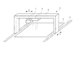
図1は実施例に係る基板印刷器の構成を示す概略斜視図であり、図2はマトリックス基板製造装置の構成を示すブロック図であり、図3はマーキングされたプラスチック基板を示す模式的正面図であり、図4から図6は積層パターンを設計してからパターン印刷することを説明する説明図であり、図7はマトリックス基板を用いた放射線検出器を作製する流れを示すフローチャート図であり、図8から図14はマトリックス基板を用いた放射線検出器の製作過程における模式的正面図であり、図15はマトリックス基板を用いた放射線検出器の製作過程における模式的縦断面図である。Embodiments of the present invention will be described below with reference to the drawings.
FIG. 1 is a schematic perspective view showing a configuration of a substrate printer according to an embodiment, FIG. 2 is a block diagram showing a configuration of a matrix substrate manufacturing apparatus, and FIG. 3 is a schematic front view showing a marked plastic substrate. FIGS. 4 to 6 are explanatory diagrams for explaining pattern printing after designing a laminated pattern, and FIG. 7 is a flowchart showing a flow of manufacturing a radiation detector using a matrix substrate. 8 to 14 are schematic front views in the process of manufacturing the radiation detector using the matrix substrate, and FIG. 15 is a schematic longitudinal sectional view in the process of manufacturing the radiation detector using the matrix substrate.
<基板印刷器>
図1に示されるように、基板印刷器1は、半導体材料および絶縁材料並びに金属インクを印刷によりプラスチック基板5の面上に積層するインクジェットノズル3と、プラスチック基板5およびプラスチック基板5に積層された積層パターンを撮像するCCDカメラ7と、インクジェットノズル3およびCCDカメラ7をX方向に駆動することができるX方向駆動装置39(図2参照)が設置された支持アーム9と、支持アーム9をY方向へレール11を介して駆動するY方向駆動装置41(図2参照)と、プラスチック基板5を支持する基板支持テーブル(図示省略)とで構成される。CCDカメラ7とインクジェットノズル3は各々独立してX方向の移動ができてもよいし、一緒にX方向に移動してもよい。プラスチック基板5は本発明における熱可塑性絶縁基板に相当する。CCDカメラ7は本発明における撮像手段に相当する。<Board printer>
As shown in FIG. 1, the
本実施例ではプラスチック基板5としてポリイミドを採用している。ポリイミドは約20ppm/℃の熱膨張率をもつ。プラスチック基板5上へ有機絶縁材料、有機半導体材料、または金属インクを印刷塗布して積層パターンを形成する場合、有機絶縁材料、有機半導体材料、または金属インクは有機溶媒により溶解または分散されているので、印刷塗布後に有機溶媒を熱処理により揮発させて硬化させなければならない。しかしながら、この熱処理によりプラスチック基板5が熱膨張を起こし、室温まで冷却した後も残留応力により元の形状に戻ることなく膨張または収縮した状態になる。特にプラスチックフィルムからプラスチック基板5を所定の大きさに切断して使用する場合、プラスチックフィルムの延伸方向に膨張または収縮しやすい。本実施例においてはX方向がこのプラスチックフィルムの延伸方向にあたる。このプラスチック基板5の膨張または収縮は非常に軽微なものであり、例えば、40cm四方のプラスチック基板5において、10〜30μm程度の膨張または収縮となる。しかしながら、この微小な膨張または収縮が、層間パターンの接続の支障をきたすことになる。
In this embodiment, polyimide is used as the
また、プラスチック基板5としては他にもポリフェニレンスルフィド(PPS)やポリエーテルスルホン(PES)なども熱膨張率が低く、プラスチック基板5として好ましい材料である。
In addition, as the
<マトリックス基板製造装置>
図2を参照して、マトリックス基板製造装置12の構成を説明する。XおよびY方向に移動するCCDカメラ7により順次撮像されたプラスチック基板5の画像は、モニター15に映し出されるとともに、ホストコンピュータ17内の撮像パターンメモリ19に画像データとして順次格納される。このようにして、プラスチック基板5上の予めマーキングされているアライメントマーク(図3参照)および積層パターンの画像データが全てインクジェット印刷の印刷ドット単位の画像データとして撮像パターンメモリ19に格納される。<Matrix substrate manufacturing equipment>
The configuration of the matrix
次に、予めプラスチック基板5上のアライメントマークを含む画像データが格納されている基本マークパターンメモリ21内の画像データと、上述した撮像パターンメモリ19に格納されている画像データとを比較器23にて比較する。基本マークパターンメモリ内の画像データは本発明における基本位置パターンに相当するもので、CCDカメラ7にて撮像された撮像パターンの位置ズレを検出するための位置基準となるものである。撮像パターンメモリ19内の画像データのアライメントマークと、基本マークパターンメモリ19内の画像データのアライメントマークとの位置を比較することで各画素ごとのX、Y方向のアライメントマークの位置ズレ量を検出する。これによりプレスチック基板5の歪みを検出することができる。ここで、撮像パターンメモリ19と基本パターンメモリ21と比較器23とで積層パターン比較部25が構成される。
Next, the image data in the basic
そして、積層パターン比較部25にて検出された各画素ごとの位置ズレ量は、各画素ごとのアドレスが振り分けられている位置ズレデータメモリ29に格納される。基本積層パターンメモリ27内には全ての層の位置ズレの無い基本積層パターンのデータが格納されており、この基本積層パターンと位置ズレデータとを基にプラスチック基板5の歪みに対応して、次に積層する印刷パターンをCPU31にて新たに設計する。そして、CPU31にて設計された積層パターンを印刷パターンメモリ33内に格納する。ここで、基本積層パターンメモリ27、位置ズレデータメモリ29、CPU31、印刷パターンメモリ33とで積層パターン設計部35が構成される。
Then, the positional deviation amount for each pixel detected by the stacked
印刷パターンメモリ33内に格納された印刷パターンデータは印刷制御部36へ送られる。印刷制御部36では、印刷パターンデータに基づきインクジェットノズル3へ印刷指示するとともに、ステージ制御部37へ位置信号を送る。この位置信号によりステージ制御部37がX方向駆動装置39およびY方向駆動装置41を制御することで、インクジェットノズル3の液滴射出と同期して、インクジェットノズル3とプラスチック基板5とのX方向およびY方向の相対位置が制御され、プラスチック基板5に印刷パターンが印刷塗布される。ここでインクジェットノズル3から射出される液滴(インク)は導線を形成する金属インクまたは有機半導体または有機絶縁体であり、有機溶媒により溶解または分散され溶液状態またはコロイド状態である。
The print pattern data stored in the
<積層パターン設計>
上述した積層パターン設計部35において設計される積層パターンは、基本積層パターンと位置ズレデータとを基に、拡大または縮小または位置補正の少なくともいずれか1つまたはそれらの組み合せにより設計されるものである。<Laminate pattern design>
The laminate pattern designed in the laminate
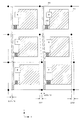
例えば、図3に示されるようなプラスチック基板5上に、図4に示されるような半導体膜42および導電体44が形成されている場合を例にとる。導電体44は半導体膜42の右端に重なって積層されており、半導体膜42の左端に配線46を積層する工程を以下に説明する。まず、CCDカメラ7でプラスチック基板5上をスキャンしてプラスチック基板5の画像データを得る。次に、積層パターン比較部25により4つのドット状のアライメントマークで決められる画素領域AからFにおいて、C、D、EおよびFの画素領域がX方向へ伸張していることが検出され、位置ズレ量ΔX1およびΔX2を測定する。ここで、積層パターン設計部35により次に積層する配線パターンを設計することなく、予め決められている基本積層パターン通りに配線パターンを印刷すれば、図5に示されるように配線46が印刷される。このように印刷すれば、画素領域Fにおいては、既に積層されていたパターンと新たに印刷した配線46との接続に不具合が生じる。
For example, the case where the
そこで、図6に示されるように、X方向への位置ズレ量ΔX1およびΔX2に対して、それぞれの位置ズレ量の半分の値である(ΔX1)/2および(ΔX2)/2だけ配線46をプラスチック基板5の位置ズレの方向へずらした積層パターンをCPU31にて設計し、この積層パターンデータにしたがって配線46を印刷する。このように、各画素領域の伸張に対応して積層パターンの位置修正を行い、最適な積層パターンを印刷することができる。本実施例では、プラスチック基板5の位置ズレ量ΔXに対して、ΔX/2だけ配線の位置補正を行っているが、これに限らず、どれだけの長さを位置補正するかは適宜選択すればよい。
Therefore, as shown in FIG. 6, the
また、プラスチック基板5がY方向へ伸張または収縮した場合も、配線46を位置ズレと対応して、拡大または縮小による補正を行う。
Further, even when the
このように、プラスチック基板5の伸張の方向により、位置補正または拡大補正のどちらの補正方法を選択するかは、各形成される素子により設計者が適宜選択すればよい。また、プラスチック基板5が収縮した場合も、位置補正または縮小補正のどちらの補正をするかは、設計者が形成される素子により適宜選択すればよい。
In this way, the designer may appropriately select which correction method to be selected, that is, position correction or enlargement correction, depending on the extension direction of the
<放射線検出器製造方法>
次に、アクティブマトリックス基板を備えた放射線検出器の製造方法について図7〜図15を参照して説明する。図7は、実施例に係るマトリックス基板製造装置12により製造されるフラットパネル型X線検出器(FPD)の製造工程の流れを示すフローチャートであり、図8〜図14は、実施例に係るフラットパネル型X線検出器(FPD)の製造工程を示す模式的平面図であり、図15は実施例に係るフラットパネル型X線検出器(FPD)の製造工程を示す模式的縦断面図である。<Radiation detector manufacturing method>
Next, a method for manufacturing a radiation detector having an active matrix substrate will be described with reference to FIGS. FIG. 7 is a flowchart showing the flow of the manufacturing process of the flat panel X-ray detector (FPD) manufactured by the matrix
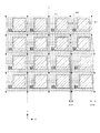
(ステップS1)マーキング
まず、プラスチック基板5上に、図3に示されるように位置合わせ用のアライメントマークをマーキングする。位置合わせ用のアライメントマークとして、本実施例では、十字形のアライメントマークとドット状のアライメントマークの2種類を形成する。十字形のアライメントマークは、撮像パターンメモリ19内の画像データと基本マークパターンメモリ21内の画像データとの画像データ同士の位置合わせに使われるもので、プラスチック基板5の熱収縮の影響がほとんど無いプラスチック基板5の内側に形成されている。ドット状のアライメントマークは、各画素領域の伸縮または収縮の距離を測定するのに用いられる。アライメントマークの形成はインクジェット法やナノインプリント、グラビア印刷などの印刷法でもよいし、他の方法により形成してもよい。また、アライメントマークの形状については、十字形やドット状にとらわれず、その他の形状であってもよい。また、図3ではドット状のアライメントマークは各画素の四方にマーキングしていたが、これにとらわれず、適宜マーキングすればよい。(Step S1) Marking First, an alignment mark for alignment is marked on the
ドット状の位置合わせ用のアライメントマークは、1画素ごとに形成され、各ドットの位置ズレを計測することで、プラスチック基板5の歪みを計測する。また、プラスチック基板5上に形成されたアライメントマークをCCDカメラ7で撮像し、各プラスチック基板5ごとにこの画像データを基本マークパターンメモリ21に格納してもよいし、もしくは、予め定められた画像データを基本マークパターンメモリ21に格納してもよい。
An alignment mark for dot alignment is formed for each pixel, and the distortion of the
(ステップS2)ゲート線・GND線形成
図8に示されるように、位置合わせ用のアライメントマークが形成されたプラスチック基板5上にグランド線43およびゲート線45を印刷塗布する。この後、乾燥炉(図示省略)にプラスチック基板5が搬送され、配線パターンが熱硬化される。位置合わせ用のアライメントマークをインクジェット法により印刷形成した場合、このゲート線・GND(グランド)線パターンの熱硬化時に熱硬化させてもよいし、ゲート線・GND線パターンの印刷前にアライメントマークを先に熱硬化させてもよい。(Step S2) Formation of Gate Line / GND Line As shown in FIG. 8, the
(ステップS3)絶縁層形成
次に、図9に示されるようにグランド線43、およびゲート線45、並びにプラスチック基板5上に絶縁層47が一様に積層される。インクジェット印刷により積層した後、乾燥炉にて乾燥させる。(Step S3) Formation of Insulating Layer Next, as shown in FIG. 9, the insulating
(ステップS4)ゲートチャンネル・キャリア収集電極形成
そして、図10に示されるように絶縁層47を挟んでゲート線45の所定の対向位置にゲートチャンネル49を形成する。インクジェット印刷により積層した後、乾燥炉にて乾燥させる。(Step S4) Formation of Gate Channel / Carrier Collection Electrode Then, as shown in FIG. 10, a
図11に示されるように、キャリア収集電極51はゲートチャンネル49を挟んで絶縁層47上に積層形成しつつ、絶縁層47を挟んでグランド線43に対向するように積層形成する。インクジェット印刷により積層した後、乾燥炉にて乾燥させる。
As shown in FIG. 11, the
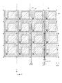
(ステップS5)データ線形成
次に、データ線を形成する前に、CCDカメラ7により、プラスチック基板5上のアライメントマークを撮像する。この結果、図12に示されるようなプラスチック基板5の歪みが計測される。図12によれば、プラスチック基板5はX方向に膨張している。CCDカメラ7により撮像されたこの画像データと基本マークパターンメモリ21内の画像データとを比較して各画素ごとの位置ズレを計測して、位置ズレデータメモリ29に各画素ごとの位置ズレのデータを格納する。基本積層パターンメモリ27内に格納されているデータ線53の配線パターンのデータに位置ズレデータを反映させて、印刷パターンをCPU31にて設計し、印刷パターンメモリ33にデータ線53の印刷パターンデータを格納する。(Step S5) Data Line Formation Next, before forming the data line, the
印刷パターンメモリ33に格納されているデータにしたがって印刷制御部36ではステージ制御部37へ位置信号を送るとともに、インクジェットノズル3へインクの吐出信号を送る。そして、ステージ制御部37へ送られてきた位置信号を基に、インクジェットノズル3が備えられているX方向駆動装置39およびY方向駆動装置41が駆動され、これと同期してデータ線53が図13に示されるように印刷される。その後、プラスチック基板5は乾燥炉に搬入されて金属インクが乾燥され、データ線53が硬化形成される。
In accordance with the data stored in the
(ステップS6)絶縁層形成
図14に示されるように、データ線53、キャリア収集電極51、ゲートチャンネル49、および絶縁層47上に絶縁膜55が積層形成される。この後積層する画素電極57と接続するためにキャリア収集電極51上には絶縁膜55を積層形成しない部分があり、キャリア収集電極51の周囲を絶縁膜55で積層形成する。開口部を始めから開けた状態で絶縁膜55を印刷塗布し、乾燥炉にて乾燥させることにより積層形成する。(Step S <b> 6) Insulating Layer Formation As shown in FIG. 14, the insulating
(ステップS7)画素電極形成
図15(a)に示されるように、キャリア収集電極51および絶縁膜55上に画素電極57を積層する。なお、ゲートチャンネル49に対向したゲート線45の一部分と、データ線53のゲートチャンネル49側の部分と、ゲートチャンネル49と、キャリア収集電極51のゲートチャンネル49側の部分と、ゲート線45/データ線53・ゲートチャンネル49・キャリア収集電極51間に介在する絶縁層47とで、薄膜トランジスタTrを構成する。また、キャリア収集電極51と、グランド線43と、キャリア収集電極51/グランド線43間に介在する絶縁層47とで、コンデンサCaを構成する。インクジェット印刷により画素電極57を積層した後、乾燥炉にて乾燥させる。(Step S <b> 7) Pixel Electrode Formation As shown in FIG. 15A, the
(ステップS8)絶縁層形成
図15(b)に示されるように、画素電極57および絶縁膜55上に絶縁膜59を積層する。この後積層する半導体層61によって生成されたキャリアを画素電極57に収集するために、半導体層61に直接に接触すべく画素電極57の大部分には絶縁膜59を積層形成せずに、画素電極57の周囲のみを絶縁膜59で積層形成する。すなわち、画素電極57の部分を開口するように絶縁膜59を積層形成する。この開口部の形成は、インクジェット法により、開口部を始めから開けた状態で絶縁膜59を印刷塗布し乾燥させることで形成する。(Step S8) Formation of Insulating Layer As shown in FIG. 15B, an insulating
(ステップS9)放射線変換層形成
図15(c)に示されるように、画素電極57および絶縁膜59上に半導体層61を積層形成する。本実施例の場合、半導体層61としてa−Seを積層するので蒸着法を用いる。半導体層19にどのような半導体を用いるかで積層方法を変えてもよい。(Step S9) Formation of Radiation Conversion Layer As shown in FIG. 15C, a
(ステップS10)電圧印加電極形成
図15(d)に示されるように、電圧印加電極63を半導体層61上に積層形成する。この後さらに、保護層(図示省略)を電圧印加電極63に積層形成することで、キャリア収集電極51、コンデンサCa、薄膜トランジスタTr、データ線53、および、ゲート線45で構成されたフラットパネル型X線検出器の一連の製造を終了する。(Step S <b> 10) Voltage Application Electrode Formation As shown in FIG. 15D, the
これらアクティブマトリックス基板の積層パターンの形成については、インクジェット法に限らず、蒸着法、スピンコート法、電界メッキ法、スパッタリング法などのフォトリソグラフィ法を組み合せてもよい。特に、アクティブマトリックス基板全体に一様に絶縁膜を形成するときなどはインクジェット法よりも有効である。 The formation of the laminated pattern of these active matrix substrates is not limited to the ink jet method, and a photolithography method such as an evaporation method, a spin coating method, an electroplating method, or a sputtering method may be combined. In particular, it is more effective than the ink jet method when an insulating film is uniformly formed on the entire active matrix substrate.
ゲートチャンネル49を形成する半導体については、インクジェットノズルにて印刷塗布する場合、ペンタセンなどの有機半導体が候補としてあげられる。しかしそれに限らず、アモルファスシリコン(a−Si)や酸化物半導体、あるいはカーボンナノチューブなどの無機物であっても良い。半導体層19を形成する放射線感応型半導体についても、上述したアモルファスセレン以外にも放射線の入射によりキャリアが生成される放射線感応型の物質、あるいは光の入射によりキャリアが生成される光感応型の物質であれば、有機半導体であってもよい。
As for the semiconductor forming the
また、グランド線43、ゲート線45、キャリア収集電極51、およびデータ線53から構成される積層パターンについて、これら積層パターンの全てを金属インクで形成してもよいし、積層パターンのすくなくとも一部を金属インクで積層形成してもよい。金属インクは銀、金、白金、銅などの金属をナノサイズ(10−9m程度)の粒子にしたものである。金属インク以外にも、導電性ポリマーの微粒子でもよい。Further, regarding the laminated pattern composed of the
上記のように構成したアクティブマトリックス基板の製造装置は、印刷描画と熱処理を繰り返してプラスチック基板に歪みが生じても、プラスチック基板の歪みに応じて次に積層する印刷パターンを設計して印刷描画できるアクティブマトリックス基板の製造装置を提供することができる。この結果、層間パターンの位置ズレによりアクティブマトリックス基板が製作できなくなる問題が解消され、アクティブマトリックス基板の製造歩留まりを向上することができる。 The active matrix substrate manufacturing apparatus configured as described above can print and draw by designing the next print pattern to be laminated according to the distortion of the plastic substrate, even if the plastic substrate is distorted by repeated printing and heat treatment. An apparatus for manufacturing an active matrix substrate can be provided. As a result, the problem that the active matrix substrate cannot be manufactured due to the displacement of the interlayer pattern is solved, and the manufacturing yield of the active matrix substrate can be improved.
この発明は、上記実施形態に限られることはなく、下記のように変形実施することができる。 The present invention is not limited to the above-described embodiment, and can be modified as follows.
(1)上述した実施例では、データ線53を印刷塗布する前にだけ印刷パターンを設計したが、これに限らず、プラスチック基板5を加熱処理するごとに、次に積層する印刷パターンの設計を行ってもよい。どの積層パターンを印刷塗布する時に印刷パターンの設計をするかは、適宜決めればよい。
(1) In the above-described embodiment, the print pattern is designed only before the
(2)上述した実施例では、基板上のドットパターンは全面にされていたが、図16に示されるように、撮像パターンメモリ19内の画像データと基本マークパターンメモリ21内の画像データとの位置合わせを行うためのアライメントマークよりも外側の領域にある画素ごとに、プラスチック基板64上にドットパターンをしてもよい。また、プラスチック基板64のロット特性を測定し、特にプラスチック基板の歪みが生じる部分にだけドットパターンを形成してもよい。また、1画素ごとにドットパターンを形成していたが、複数の画素ごとにドットパターンを形成してもよい。また、積層パターン形成ごとに新たにドットパターンを形成してもよい。
(2) In the embodiment described above, the dot pattern on the substrate is the entire surface, but as shown in FIG. 16, the image data in the
(3)上述した実施例では、プラスチック基板5上に形成されたアライメントマークをプラスチック基板5の歪みを計測する位置基準としたが、基板上の積層パターンそのものを位置基準としてもよい。つまり、基本マークパターンメモリ21に格納される画像データはプラスチック基板5上に形成されたアライメントマークの位置基準となるものであってもよいし、プラスチック基板5上に形成された積層パターンの位置基準となるものであってもよい。また、基本マークパターンメモリ21に格納される画像データは、予め格納された画像データであってもよいし、CCDカメラ7によって撮像された画像データであってもよい。また、CCDカメラ7によって撮像された画像データを基本マークパターンメモリ21に格納される画像データとする場合、アライメントマークまたは第1層目の積層パターンであってもよいし、1つ前に積層された積層パターンまたは1つ前に形成されたドットパターンであってもよい。
(3) In the embodiment described above, the alignment mark formed on the
(4)上述した実施例では、ボトムゲート型の薄膜トランジスタ(TFT)を備えたアクティブマトリックス基板であったが、トップゲート型のTFTを備えたアクティブマトリックス基板であってもよい。図15(d)に示されるように、薄膜トランジスタのゲート(ゲート線45)をTFTのソース(キャリア収集電極51)・ドレイン(データ配線53)よりもプラスチック基板5側に形成したが、TFTソース・ドレインをTFTゲートよりもプラスチック基板5側に形成してもよい。このような設計に応じて各電極等の形成位置を適宜変更すればよい。本願のマトリックス基板製造装置によりトップゲート型のアクティブマトリックス基板を製造すれば、コンタクトホールを開ける際にも、プラスチック基板5に歪みが生じていても下層にパターニングされている素子との位置関係を確認してからコンタクトホールを開けることができるので有効である。
(4) In the above-described embodiments, the active matrix substrate is provided with a bottom gate type thin film transistor (TFT), but may be an active matrix substrate provided with a top gate type TFT. As shown in FIG. 15D, the gate (gate line 45) of the thin film transistor is formed closer to the
(5)上述した実施例では、インクジェットノズル3がX方向に移動し、インクジェットノズル3を搭載した支持アーム9がY方向に移動したが、プラスチック基板5を支持する基板支持テーブルがXY方向に移動してもよい。例えば、図17に示されるように、プラスチック基板5を支持する基板支持テーブル65の下部にはX方向テーブル駆動装置66とY方向テーブル駆動装置67が備えられており、支持アーム68に備えられたインクジェットノズル3およびCCDカメラ7に対してプラスチック基板5が載置された基板支持テーブル65がXY方向に移動する。また、インクジェットノズル3がX方向へ移動し、基板支持テーブルがY方向に移動する構成でもよい。
(5) In the above-described embodiment, the
(6)上述した実施例では、マトリックス基板製造装置にてアクティブマトリックス基板を製造したが、パッシブマトリクス基板を製造してもよい。 (6) In the embodiment described above, the active matrix substrate is manufactured by the matrix substrate manufacturing apparatus, but a passive matrix substrate may be manufactured.
(7)上述した実施例では、受光デバイスとしての放射線検出器に備わるアクティブマトリックス基板であったが、発光デバイスとしての液晶ディスプレイなどに使われるアクティブマトリックス基板であってもよい。 (7) In the above-described embodiments, the active matrix substrate is provided in the radiation detector as the light receiving device, but it may be an active matrix substrate used in a liquid crystal display as the light emitting device.
(8)上述した実施例では、アライメントマークは十字形のものと、ドット状のものであったが、アライメントマークの直近に、基板内での絶対座標位置を示す数字、文字、パターンコードを含むものであってもよいし、さらにはアライメントマーク自身をそれらの数字、文字、パターンコードとするものであってもよい。絶対座標位置を示す記号を入れることで、CCDによる検索(次のアライメントマークへの移動)が素早くできるようになるという効果が生じる。 (8) In the above-described embodiments, the alignment marks are cross-shaped and dot-shaped, but include numbers, characters, and pattern codes that indicate absolute coordinate positions in the substrate immediately adjacent to the alignment marks. The alignment mark itself may be those numbers, characters, and pattern codes. By inserting a symbol indicating the absolute coordinate position, there is an effect that the search by the CCD (movement to the next alignment mark) can be performed quickly.
Claims (4)
前記熱可塑性絶縁基板および前記熱可塑性絶縁基板上に積層された積層パターンを撮像する撮像手段と、
前記撮像手段により撮像された撮像パターンと前記熱可塑性絶縁基板または前記熱可塑性絶縁基板上に積層された積層パターンの位置基準となる基本位置パターンとを比較し、前記熱可塑性絶縁基板の画素領域ごとの歪みを検出する積層パターン比較部と、
前記積層パターン比較部より求められた前記熱可塑性絶縁基板の画素領域ごとの歪みに応じて、次に前記熱可塑性絶縁基板上に積層する積層パターンを設計する積層パターン設計部と、
前記積層パターン設計部より設計された積層パターンの印刷を制御する印刷制御部と、
前記印刷制御部により送られる印刷信号によりインクを射出するインクジェットノズルと、
前記印刷制御部より送られる駆動信号により前記インクジェットノズルと前記熱可塑性絶縁基板との相対位置を制御するステージ機構部と
を備え、
前記基本位置パターンが、比較される前記撮像パターンよりも過去に前記熱可塑性絶縁基板上に形成された積層パターンである
ことを特徴とするマトリックス基板製造装置。 In a matrix substrate manufacturing apparatus in which a semiconductor or a conductor or an insulator is laminated on a thermoplastic insulating substrate,
Imaging means for imaging the thermoplastic insulating substrate and a laminated pattern laminated on the thermoplastic insulating substrate;
The image pickup pattern picked up by the image pickup means is compared with the basic position pattern serving as a position reference of the thermoplastic insulating substrate or the laminated pattern laminated on the thermoplastic insulating substrate, for each pixel region of the thermoplastic insulating substrate. A laminated pattern comparison unit for detecting the distortion of
In accordance with the distortion for each pixel region of the thermoplastic insulating substrate obtained from the laminated pattern comparison unit, a laminated pattern design unit that designs a laminated pattern to be laminated on the thermoplastic insulating substrate next,
A print control unit that controls printing of the laminated pattern designed by the laminated pattern design unit;
An inkjet nozzle that ejects ink in accordance with a print signal sent by the print control unit;
A stage mechanism unit that controls a relative position between the inkjet nozzle and the thermoplastic insulating substrate by a drive signal sent from the print control unit;
The matrix substrate manufacturing apparatus, wherein the basic position pattern is a laminated pattern formed on the thermoplastic insulating substrate in the past than the imaging pattern to be compared.
前記ステージ機構部は、前記インクジェットノズルを搭載した架台に前記インクジェットノズルがX方向に移動可能な機構を設けたX方向駆動器と、
前記架台がY方向に移動可能な機構を設けたY方向駆動器と
を備えたことを特徴とするマトリックス基板製造装置。 In the matrix substrate manufacturing apparatus according to claim 1,
The stage mechanism unit includes an X-direction driver in which a mechanism on which the inkjet nozzle can move in the X direction is provided on a mount on which the inkjet nozzle is mounted;
A matrix substrate manufacturing apparatus comprising: a Y-direction driver provided with a mechanism in which the mount is movable in the Y direction.
Applications Claiming Priority (1)
| Application Number | Priority Date | Filing Date | Title |
|---|---|---|---|
| PCT/JP2008/058107 WO2009130791A1 (en) | 2008-04-25 | 2008-04-25 | Matrix substrate manufacturing apparatus |
Publications (2)
| Publication Number | Publication Date |
|---|---|
| JPWO2009130791A1 JPWO2009130791A1 (en) | 2011-08-11 |
| JP5218552B2 true JP5218552B2 (en) | 2013-06-26 |
Family
ID=41216540
Family Applications (1)
| Application Number | Title | Priority Date | Filing Date |
|---|---|---|---|
| JP2010509018A Expired - Fee Related JP5218552B2 (en) | 2008-04-25 | 2008-04-25 | Matrix substrate manufacturing equipment |
Country Status (2)
| Country | Link |
|---|---|
| JP (1) | JP5218552B2 (en) |
| WO (1) | WO2009130791A1 (en) |
Families Citing this family (2)
| Publication number | Priority date | Publication date | Assignee | Title |
|---|---|---|---|---|
| JP2020131141A (en) * | 2019-02-21 | 2020-08-31 | 紀州技研工業株式会社 | Drawing method and drawing device |
| US20240422916A1 (en) * | 2021-11-04 | 2024-12-19 | Fuji Corporation | Circuit-forming method and circuit-forming apparatus |
Citations (5)
| Publication number | Priority date | Publication date | Assignee | Title |
|---|---|---|---|---|
| JPH09213212A (en) * | 1996-02-06 | 1997-08-15 | Canon Inc | INKJET DROPLET APPARATUS, ELECTRON SOURCE SUBSTRATE USING SAME, AND METHOD FOR MANUFACTURING IMAGE FORMING APPARATUS |
| JP2000251665A (en) * | 1998-02-13 | 2000-09-14 | Canon Inc | Method of forming film, method of manufacturing electron-emitting device using the same, and method of manufacturing image forming apparatus using the same |
| JP2005043424A (en) * | 2003-07-22 | 2005-02-17 | Ricoh Co Ltd | Pattern formation method |
| JP2005535147A (en) * | 2002-08-30 | 2005-11-17 | シャープ株式会社 | THIN FILM TRANSISTOR, LIQUID CRYSTAL DISPLAY DEVICE, METHOD FOR PRODUCING THIN FILM TRANSISTOR AND METHOD FOR MANUFACTURING LIQUID CRYSTAL DISPLAY DEVICE |
| JP2007110048A (en) * | 2005-10-17 | 2007-04-26 | Ricoh Co Ltd | Inkjet pattern formation method, inkjet pattern formation apparatus, electronic element array, display element |
-
2008
- 2008-04-25 WO PCT/JP2008/058107 patent/WO2009130791A1/en not_active Ceased
- 2008-04-25 JP JP2010509018A patent/JP5218552B2/en not_active Expired - Fee Related
Patent Citations (5)
| Publication number | Priority date | Publication date | Assignee | Title |
|---|---|---|---|---|
| JPH09213212A (en) * | 1996-02-06 | 1997-08-15 | Canon Inc | INKJET DROPLET APPARATUS, ELECTRON SOURCE SUBSTRATE USING SAME, AND METHOD FOR MANUFACTURING IMAGE FORMING APPARATUS |
| JP2000251665A (en) * | 1998-02-13 | 2000-09-14 | Canon Inc | Method of forming film, method of manufacturing electron-emitting device using the same, and method of manufacturing image forming apparatus using the same |
| JP2005535147A (en) * | 2002-08-30 | 2005-11-17 | シャープ株式会社 | THIN FILM TRANSISTOR, LIQUID CRYSTAL DISPLAY DEVICE, METHOD FOR PRODUCING THIN FILM TRANSISTOR AND METHOD FOR MANUFACTURING LIQUID CRYSTAL DISPLAY DEVICE |
| JP2005043424A (en) * | 2003-07-22 | 2005-02-17 | Ricoh Co Ltd | Pattern formation method |
| JP2007110048A (en) * | 2005-10-17 | 2007-04-26 | Ricoh Co Ltd | Inkjet pattern formation method, inkjet pattern formation apparatus, electronic element array, display element |
Also Published As
| Publication number | Publication date |
|---|---|
| JPWO2009130791A1 (en) | 2011-08-11 |
| WO2009130791A1 (en) | 2009-10-29 |
Similar Documents
| Publication | Publication Date | Title |
|---|---|---|
| JP4168934B2 (en) | Manufacturing method of semiconductor device | |
| US7765686B2 (en) | Multilayer wiring structure and method of manufacturing the same | |
| JP5478608B2 (en) | Offset upper pixel electrode configuration | |
| US8598570B2 (en) | Organic transistor array, display device and method of fabricating display device | |
| CN1512939A (en) | Inkjet deposition apparatus and method | |
| JP6115008B2 (en) | WIRING MEMBER, ELECTRONIC ELEMENT MANUFACTURING METHOD, WIRING MEMBER, LAMINATED WIRING, ELECTRONIC ELEMENT, ELECTRONIC ELEMENT ARRAY, AND DISPLAY DEVICE USING THE SAME | |
| US9304097B2 (en) | Method for aligning patterns on a substrate | |
| JP5978577B2 (en) | Multilayer wiring board | |
| US9291588B2 (en) | System for forming aligned patterns on a substrate | |
| US9228964B2 (en) | System for aligning patterns on a substrate | |
| US10580956B2 (en) | Method for producing a stack of layers for a matrix thermal sensor | |
| US9291587B2 (en) | Method for forming aligned patterns on a substrate | |
| JP5218552B2 (en) | Matrix substrate manufacturing equipment | |
| JP5689007B2 (en) | Thin film transistor manufacturing apparatus and manufacturing method thereof | |
| US9274431B2 (en) | Alignment structure for registering patterns on a substrate | |
| WO2009139060A1 (en) | Process for producing light matrix device and apparatus for producing light matrix device | |
| JP2010135584A (en) | Thin film transistor, method of manufacturing thin film transistor, display device, and electronic apparatus | |
| JP5304897B2 (en) | Manufacturing method of optical matrix device | |
| JP2007110048A (en) | Inkjet pattern formation method, inkjet pattern formation apparatus, electronic element array, display element | |
| JP5073194B2 (en) | Flat panel display and manufacturing method thereof | |
| JP5887881B2 (en) | Wiring formation method | |
| JP5514545B2 (en) | Distortion-tolerant processing | |
| JP5342862B2 (en) | Manufacturing method of optical matrix device | |
| CN102227810A (en) | Method for fabricating optical matrix device | |
| Street et al. | Printed active-matrix TFT arrays for x-ray imaging |
Legal Events
| Date | Code | Title | Description |
|---|---|---|---|
| A131 | Notification of reasons for refusal |
Free format text: JAPANESE INTERMEDIATE CODE: A131 Effective date: 20121113 |
|
| A521 | Request for written amendment filed |
Free format text: JAPANESE INTERMEDIATE CODE: A523 Effective date: 20130111 |
|
| TRDD | Decision of grant or rejection written | ||
| A01 | Written decision to grant a patent or to grant a registration (utility model) |
Free format text: JAPANESE INTERMEDIATE CODE: A01 Effective date: 20130205 |
|
| A61 | First payment of annual fees (during grant procedure) |
Free format text: JAPANESE INTERMEDIATE CODE: A61 Effective date: 20130218 |
|
| FPAY | Renewal fee payment (event date is renewal date of database) |
Free format text: PAYMENT UNTIL: 20160315 Year of fee payment: 3 |
|
| FPAY | Renewal fee payment (event date is renewal date of database) |
Free format text: PAYMENT UNTIL: 20160315 Year of fee payment: 3 |
|
| LAPS | Cancellation because of no payment of annual fees |