JP5214422B2 - Data storage system - Google Patents
Data storage system Download PDFInfo
- Publication number
- JP5214422B2 JP5214422B2 JP2008311551A JP2008311551A JP5214422B2 JP 5214422 B2 JP5214422 B2 JP 5214422B2 JP 2008311551 A JP2008311551 A JP 2008311551A JP 2008311551 A JP2008311551 A JP 2008311551A JP 5214422 B2 JP5214422 B2 JP 5214422B2
- Authority
- JP
- Japan
- Prior art keywords
- bit
- bits
- code
- information
- circuit
- Prior art date
- Legal status (The legal status is an assumption and is not a legal conclusion. Google has not performed a legal analysis and makes no representation as to the accuracy of the status listed.)
- Expired - Fee Related
Links
Images
Classifications
-
- G—PHYSICS
- G11—INFORMATION STORAGE
- G11C—STATIC STORES
- G11C16/00—Erasable programmable read-only memories
- G11C16/02—Erasable programmable read-only memories electrically programmable
- G11C16/06—Auxiliary circuits, e.g. for writing into memory
- G11C16/34—Determination of programming status, e.g. threshold voltage, overprogramming or underprogramming, retention
- G11C16/3418—Disturbance prevention or evaluation; Refreshing of disturbed memory data
- G11C16/3427—Circuits or methods to prevent or reduce disturbance of the state of a memory cell when neighbouring cells are read or written
-
- G—PHYSICS
- G06—COMPUTING; CALCULATING OR COUNTING
- G06F—ELECTRIC DIGITAL DATA PROCESSING
- G06F11/00—Error detection; Error correction; Monitoring
- G06F11/07—Responding to the occurrence of a fault, e.g. fault tolerance
- G06F11/08—Error detection or correction by redundancy in data representation, e.g. by using checking codes
- G06F11/10—Adding special bits or symbols to the coded information, e.g. parity check, casting out 9's or 11's
- G06F11/1008—Adding special bits or symbols to the coded information, e.g. parity check, casting out 9's or 11's in individual solid state devices
- G06F11/1068—Adding special bits or symbols to the coded information, e.g. parity check, casting out 9's or 11's in individual solid state devices in sector programmable memories, e.g. flash disk
-
- G—PHYSICS
- G11—INFORMATION STORAGE
- G11C—STATIC STORES
- G11C11/00—Digital stores characterised by the use of particular electric or magnetic storage elements; Storage elements therefor
- G11C11/56—Digital stores characterised by the use of particular electric or magnetic storage elements; Storage elements therefor using storage elements with more than two stable states represented by steps, e.g. of voltage, current, phase, frequency
- G11C11/5621—Digital stores characterised by the use of particular electric or magnetic storage elements; Storage elements therefor using storage elements with more than two stable states represented by steps, e.g. of voltage, current, phase, frequency using charge storage in a floating gate
- G11C11/5628—Programming or writing circuits; Data input circuits
-
- G—PHYSICS
- G11—INFORMATION STORAGE
- G11C—STATIC STORES
- G11C16/00—Erasable programmable read-only memories
- G11C16/02—Erasable programmable read-only memories electrically programmable
- G11C16/04—Erasable programmable read-only memories electrically programmable using variable threshold transistors, e.g. FAMOS
- G11C16/0483—Erasable programmable read-only memories electrically programmable using variable threshold transistors, e.g. FAMOS comprising cells having several storage transistors connected in series
-
- G—PHYSICS
- G11—INFORMATION STORAGE
- G11C—STATIC STORES
- G11C16/00—Erasable programmable read-only memories
- G11C16/02—Erasable programmable read-only memories electrically programmable
- G11C16/06—Auxiliary circuits, e.g. for writing into memory
- G11C16/10—Programming or data input circuits
-
- G—PHYSICS
- G11—INFORMATION STORAGE
- G11C—STATIC STORES
- G11C16/00—Erasable programmable read-only memories
- G11C16/02—Erasable programmable read-only memories electrically programmable
- G11C16/06—Auxiliary circuits, e.g. for writing into memory
- G11C16/34—Determination of programming status, e.g. threshold voltage, overprogramming or underprogramming, retention
- G11C16/3418—Disturbance prevention or evaluation; Refreshing of disturbed memory data
-
- G—PHYSICS
- G11—INFORMATION STORAGE
- G11C—STATIC STORES
- G11C19/00—Digital stores in which the information is moved stepwise, e.g. shift registers
-
- G—PHYSICS
- G11—INFORMATION STORAGE
- G11C—STATIC STORES
- G11C29/00—Checking stores for correct operation ; Subsequent repair; Testing stores during standby or offline operation
-
- G—PHYSICS
- G11—INFORMATION STORAGE
- G11C—STATIC STORES
- G11C7/00—Arrangements for writing information into, or reading information out from, a digital store
- G11C7/10—Input/output [I/O] data interface arrangements, e.g. I/O data control circuits, I/O data buffers
- G11C7/1006—Data managing, e.g. manipulating data before writing or reading out, data bus switches or control circuits therefor
-
- G—PHYSICS
- G11—INFORMATION STORAGE
- G11C—STATIC STORES
- G11C8/00—Arrangements for selecting an address in a digital store
- G11C8/04—Arrangements for selecting an address in a digital store using a sequential addressing device, e.g. shift register, counter
Description
この発明は、データ記憶システムに関し、例えば、半導体記憶装置を含み、不良ビットが生じても救済可能な信頼性の高いシステムに適用され、特に、誤書き込みや隣接セルの容量干渉によるマージン低下に対する信頼性の向上を目的とする半導体記憶装置等に適用されるものである。 The present invention relates to a data storage system and is applied to a highly reliable system that includes a semiconductor storage device and can be relieved even if a defective bit occurs, and is particularly reliable for margin reduction due to erroneous writing or capacity interference of adjacent cells. The present invention is applied to a semiconductor memory device or the like for improving the performance.
半導体記憶装置によるデータ記憶システムのうち、例えば、電荷蓄積層にチャネルから絶縁膜を介してトンネル電流によって注入した電荷をディジタルビットの情報格納として用い、その電荷量に応じたMOSFETのコンダクタンス変化を測定し,情報を読み出す不揮発性半導体メモリ(EEPROM)が開発されている。中でも、メモリセルを複数個直列または並列接続しメモリセルブロックを形成したNAND型EEPROM(NAND型フラッシュメモリ)は、選択トランジスタゲートの数をメモリセルよりも大幅に減らすことができ、より高密度化することができる。また、NAND型EEPROMでは、メモリセルの形成されたウェルを共通化することにより、消去を複数のメモリセルで構成されたページにて一括で行う構造をとり、書き込みは個々のメモリセルについて行う構造をとるため、より高密度化することができる。ここで、上記不揮発性メモリでは、DRAMと異なりデータ破壊を伴わずに複数回読み出すことが可能である。 In a data storage system using semiconductor memory devices, for example, the charge injected by tunnel current from the channel through the insulating film to the charge storage layer is used as digital bit information storage, and the change in MOSFET conductance according to the amount of charge is measured. However, nonvolatile semiconductor memories (EEPROMs) that read information have been developed. Above all, NAND type EEPROM (NAND type flash memory) in which multiple memory cells are connected in series or in parallel to form a memory cell block can greatly reduce the number of select transistor gates compared to memory cells, resulting in higher density. can do. In addition, in the NAND type EEPROM, the well in which the memory cells are formed is made common so that erasing is performed collectively on a page composed of a plurality of memory cells, and writing is performed on each memory cell. Therefore, the density can be increased. Here, unlike the DRAM, the non-volatile memory can be read a plurality of times without data destruction.
しかし、微細化および高密度化の更なる進行によって、隣接セルの容量結合が大きくなると、隣接セルの電荷蓄積層の電荷量によって、しきい値が変化するようになると、情報ビット間のしきい値電圧余裕が低下する。特に、NAND型フラッシュメモリでは、書き込み時のデータパターンによって、一括消去した消去ビットでも消去状態を保つべきビットが書き込みビットに変化する誤書き込みが生じ、さらなるしきい値電圧余裕が低下するという問題があった。 However, if the capacitive coupling between adjacent cells increases due to further progress in miniaturization and densification, the threshold between the information bits changes as the threshold value changes depending on the amount of charge in the charge storage layer of the adjacent cells. The value voltage margin decreases. In particular, NAND flash memory has a problem that due to the data pattern at the time of writing, erroneous writing occurs in which a bit to be erased changes to a writing bit even when erased at once, and the threshold voltage margin further decreases. there were.
このような誤りビットの問題を緩和する一つの解として、例えば、本発明者らが開示する特許文献1のように、ECC(Error Correcting Code)を用いて誤り訂正を用いる方法がある。しかしながら、上記消去しきい値や書き込みしきい値が、隣接メモリセルが消去しきい値から書き込みしきい値になることにより容量結合によって上昇する問題や、隣接メモリセルのパターンによって、より誤書き込みが生じる問題に対して、より特徴を捉えた、効果があるECC構成方法については開示されていない。
As one solution to alleviate such a problem of error bits, there is a method of using error correction using ECC (Error Correcting Code) as in
より具体的には、ECCとしてBCH(Bose-Chaudhuri-Hocquenghem)符号、RS(Reed-Solomon)符号を用いた場合、例えば、BCH符号では、t重誤り訂正符号として、符号長nはmを自然数として、2m−1で固定されており、対応する情報ビット数k0はk0=2m−1−mtに制限されている。また、RS符号では、t重誤り訂正符号として、1バイトをmビットとして、符号長nは2m−1(バイト)であり、対応する情報バイト数k1はk1=2m−1−2tに制限されている。このように、ECCとしてBCH(Bose-Chaudhuri-Hocquenghem)符号等を用いた場合には、従来、短縮化符号などの手法に用いられ、符号長などの制限により自由度が小さい。 More specifically, when a BCH (Bose-Chaudhuri-Hocquenghem) code and an RS (Reed-Solomon) code are used as the ECC, for example, in the BCH code, the code length n is a natural number as a t-double error correction code. as is fixed at 2 m -1, corresponding information bit number k0 is limited to k0 = 2 m -1-mt. Further, in the RS code, as a t-heavy error correction code, 1 byte is m bits, the code length n is 2 m −1 (bytes), and the corresponding number of information bytes k1 is k1 = 2 m −1-2t. Limited. As described above, when a BCH (Bose-Chaudhuri-Hocquenghem) code or the like is used as the ECC, it is conventionally used for a method such as a shortened code, and the degree of freedom is small due to a restriction on the code length or the like.
上記のように、従来のBCH短縮符号作成法やRS短縮符号作成法のみでは、例えば、”010”など符号の特定の連パターンに対して誤りに強い訂正方法ではなく、ランダムな単ビット、または、ランダムな一定数のバイトに対する誤り訂正方法であった。 As described above, the conventional BCH abbreviated code creation method and the RS abbreviated code creation method alone are not a correction method resistant to errors with respect to a specific continuous pattern of codes such as “010”, but random single bits, or It was an error correction method for a fixed number of random bytes.
よって、上記消去しきい値や書き込みしきい値が、隣接メモリセルが消去しきい値から書き込みしきい値になることによる容量結合によって上昇する問題や、隣接メモリセルのパターンによって、より誤書き込みが生じる問題に対して、よりこの問題の特徴を捉えて解決されるものではない。従って、従来、BCH符号やRS符号と組み合わせた場合であっても、より効果がある符号化の構成方法については開示されていない。 Therefore, the above-mentioned erase threshold value and write threshold value may increase due to capacitive coupling due to the adjacent memory cell being changed from the erase threshold value to the write threshold value, and more erroneous writing may occur depending on the adjacent memory cell pattern. The problem that arises cannot be solved by capturing the characteristics of this problem. Therefore, conventionally, even when combined with a BCH code or an RS code, a more effective coding configuration method is not disclosed.
上記のように、従来のデータ記憶システムは、上記消去しきい値や書き込みしきい値が容量結合によって変化し、隣接メモリセルのパターンによって誤書き込みが生じるランダマイズに対して、ランダムな単ビット、または、ランダムな一定数のバイトに対する誤り訂正する構成であった。その結果、例えば、”010”など符号の特定の連パターンに対して、より特徴を捉えた、誤りに強い訂正をすることができない、という問題があった。
この発明は、符号の特定の連パターンに対して、より特徴を捉えた、誤り訂正に有利なデータ記憶システムを提供する。 The present invention provides a data storage system that is more advantageous for error correction and captures more features with respect to a specific pattern of codes.
この発明の一態様によれば、少なくとも"1"と"0"の2値のディジタルデータを電荷蓄積層の電荷として記憶し前記電荷蓄積層の2つの電荷量の差を書き込みビットおよび消去ビットとして用いるメモリセルを備え、複数の前記メモリセルが隣接して構成されるページを一括消去する不揮発性メモリセルアレイと、情報ビットから少なくとも1ビットの誤りデータを訂正する符号を発生し、前記ページに記録する誤り訂正符号を生成する誤り訂正符号発生回路と、前記ページに記録されたディジタルデータより、前記誤り訂正符号から誤りを訂正し前記情報ビットを復元する誤り訂正符号復号回路と、入力された前記情報ビットと”書き込みビット−消去ビット”の並びを複数回繰り返した複数ビットとの排他的論理和をとり、前記誤り訂正符号発生回路に出力する符号変換回路とを具備するデータ記憶システムを提供できる。 According to one aspect of the present invention, at least binary digital data of “1” and “0” is stored as charges in a charge storage layer, and a difference between two charge amounts in the charge storage layer is used as a write bit and an erase bit. A nonvolatile memory cell array that includes a memory cell to be used and erases a page including a plurality of memory cells adjacent to each other, and a code that corrects at least one bit of error data from an information bit is generated and recorded on the page An error correction code generation circuit that generates an error correction code to be corrected, an error correction code decoding circuit that corrects an error from the error correction code and restores the information bits from the digital data recorded on the page, and the input information bits and - taking the exclusive OR of the plurality of bits is repeated a plurality of times a sequence of "write bit erase bits", the error correction code generator It can provide data storage system comprising a code conversion circuit for outputting the road.
この発明によれば、符号の特定の連パターンに対して、より特徴を捉えた、誤り訂正に有利なデータ記憶システムが得られる。 According to the present invention, it is possible to obtain a data storage system that is more advantageous for error correction and that captures more features with respect to a specific continuous pattern of codes.
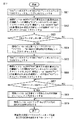
[比較例]
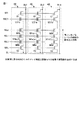
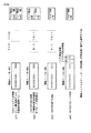
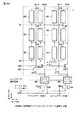
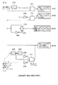
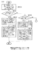
まず、以下に説明するこの発明に係る実施例1乃至実施例7に係るデータ記憶システムと比較するために、図1乃至図3を用いて、比較例に係るデータ記憶システムについて説明する。図1は、比較例に係るNAND型EEPROM半導体装置のメモリセルエレメントの回路構成を示す。
[Comparative example]
First, in order to compare with the data storage system according to the first to seventh embodiments of the present invention described below, the data storage system according to the comparative example will be described with reference to FIGS. FIG. 1 shows a circuit configuration of a memory cell element of a NAND type EEPROM semiconductor device according to a comparative example.
図1に示すように、電荷蓄積電極を有するMOSトランジスタからなる不揮発性メモリセルM0〜M31が直列に接続され、一端が選択トランジスタS1を介してBLと記してあるデータ転送線に接続されている。また他の一端は選択トランジスタS2を介してSLと記してある共通ソース線に接続されている。また、それぞれのトランジスタは、同一のp型ウェル23上に形成されている。また、それぞれのメモリセルM0〜M31の制御電極は、WL0〜WL31と記したデータ選択線(以下WLと記載する)に接続されている。また、データ転送線に沿った複数のメモリセルブロックから1つのメモリセルブロックを選択してデータ転送線に接続するため、選択トランジスタS1の制御電極はブロック選択線SSLに接続されている。さらに、選択トランジスタS2の制御電極はブロック選択線GSLに接続されており、いわゆるNAND型メモリセルブロック49(点線の領域)を形成している。ここで、本比較例では、選択ゲートの制御配線SSLおよびGSLがメモリセルエレメントの制御配線WL0〜WL31の電荷蓄積層26と同じ層の導電体によって、紙面左右方向に隣接するセルで接続されて形成されている。本比較例では、図を過剰に複雑にせず問題点を判りやすくするために、例として、3つのデータ転送線(BL1,BL2,BL3)に接続されたメモリセルアレイ構造を示して説明する。しかし、勿論、この並列数は3ではなく、もっと多数、例えば、2100個、4200個、8400個、16800個、33600個程度並列接続した構造を想定している。
As shown in FIG. 1, nonvolatile memory cells M0 to M31 made of MOS transistors having charge storage electrodes are connected in series, and one end is connected to a data transfer line denoted by BL via a select transistor S1. . The other end is connected to a common source line labeled SL through a selection transistor S2. Each transistor is formed on the same p-
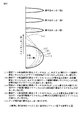
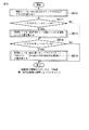
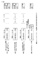
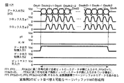
ここで、隣接するメモリセルの容量結合によって、電荷蓄積電極の電位が変化する問題を説明するために、例えば、WL1とBL2の交点に形成されたM1a(α)セルについてのしきい値分布を、例えば、図2に示す。電荷蓄積層を有する多値メモリセルにおいては、隣接するメモリセルに負の電荷が蓄積することにより、隣接するメモリセル間の容量結合を通じて、しきい値が上昇する問題が生じる。この問題を説明するために、M1a(α)セルを例として、BL方向に隣接するメモリセルM1b(β)およびM1b’(γ)、および、WL方向のS1端子側に隣接し直列接続されたメモリセルM2a(ε)が消去状態から書き込み状態に変化した場合のしきい値変動を図2に示す。 Here, in order to explain the problem that the potential of the charge storage electrode changes due to capacitive coupling of adjacent memory cells, for example, the threshold distribution for the M1a (α) cell formed at the intersection of WL1 and BL2 For example, as shown in FIG. In a multi-value memory cell having a charge storage layer, negative charges are stored in adjacent memory cells, thereby causing a problem that the threshold value is increased through capacitive coupling between adjacent memory cells. To explain this problem, taking M1a (α) cell as an example, memory cells M1b (β) and M1b ′ (γ) adjacent in the BL direction, and adjacent to the S1 terminal side in the WL direction and connected in series FIG. 2 shows threshold fluctuations when the memory cell M2a (ε) changes from the erased state to the written state.
図2では、(i)に、隣接データ転送線側の隣接メモリセル(β、γ)、および、S1側のワード線側の隣接メモリセル(ε)がすべて消去状態のメモリセルαの消去しきい値分布を示す。また、図2には、4値の書き込み状態を考え、例えば、4値の記憶を想定して、しきい値が高い側から書き込みしきい値3、書き込みしきい値2、書き込みしきい値1の順で書き込みしきい値が設定されているとする。
In FIG. 2, (i) shows that the adjacent memory cells (β, γ) on the adjacent data transfer line side and the adjacent memory cells (ε) on the S1 side word line side are all erased. The threshold distribution is shown. FIG. 2 shows a four-value write state. For example, assuming four-value storage, write
また、(ii)に、隣接データ転送線側の隣接メモリセル1セル(γ)が書き込み状態で、反対側に隣接するメモリセル(β)、および、S1側のワード線側の隣接メモリセル(ε)が消去状態の場合のメモリセルαの消去しきい値分布を示す。この場合、隣接するメモリセル1セル(γ)が書き込み状態なので、消去状態よりも電子が蓄積された状態となっている。よって、(i)に比べ、隣接メモリセルの容量結合によって、αのメモリセルのしきい値が上昇する。さらに、いわゆる誤書き込みによって(i)に比べしきい値が上昇し上裾分布が発生する問題があるが、これを以下詳細に説明する。ここで、NANDフラッシュメモリでは、データ選択線に共通に接続されたメモリセルはデータ選択線であるWLの電位を、例えば15V程度以上30V程度以下の電位を印加し、かつ、電気的に接続されたデータ転送線(BL)電位を0Vとして、書き込みを選択したメモリセルのソース電極およびドレイン電極を例えば0Vとし、チャネル電位も0Vとする。一方、書き込みを選択せず、消去状態に保つメモリセル、つまり、いわゆる非選択メモリセルのソース電極、ドレイン電極、および、チャネル電位は、例えば、5Vから10Vの間に保つことにより、データ選択線とデータ転送線との電位差を小さくすることにより、書き込みを防ぐことが行われる。なお、非選択メモリセルを実現するには、電気的に接続されたBLの電位を0Vより上昇させることによって行う。さらに、NANDフラッシュメモリでは、書き込みしきい値の分布幅を小さくするために、書き込み後にベリファイ読み出しを行うことにより、書き込みの下限しきい値(書き込みベリファイしきい値)に達したメモリセルについては、BLの電位を選択的に0Vから上昇させることにより、追加書き込みが生じないようにしている。
In (ii),
ここで、WL1に接続されたメモリセルαを消去状態に保ち、WL1に接続された別のメモリセルを書き込むために、WL1の電位を15V程度以上30V程度以下の電位を印加する場合を考える。この場合、(ii)の状態の書き込み時に、書き込みを行うメモリセルγのソース電極、ドレイン電極、およびチャネル電位は0Vであり、メモリセルαのソース電極、ドレイン電極、およびチャネル電位は5V程度から10V程度に保たれる。 Here, a case is considered in which a potential of about 15V to about 30V is applied to WL1 in order to keep the memory cell α connected to WL1 in the erased state and write another memory cell connected to WL1. In this case, at the time of writing in the state (ii), the source electrode, the drain electrode, and the channel potential of the memory cell γ to be written are 0V, and the source electrode, the drain electrode, and the channel potential of the memory cell α are from about 5V. It is kept at around 10V.
一方、(i)の状態の書き込み時には、メモリセルγとメモリセルαのソース電極、ドレイン電極、およびチャネル電位は5V程度から10V程度に保たれる。よって、(ii)の状態の書き込みの場合には、メモリセルαのソース電極またはドレイン電極から、メモリセルγのソース電極またはドレイン電極へ電流が流れることにより、メモリセルαのソース電極またはドレイン電極の電位が低下する。または、隣接するメモリセルγのソース電極およびドレイン電極の電位、およびチャネル部分の電位が(i)よりも(ii)の場合に低いことにより、BL方向の容量結合により、メモリセルαのチャネル部分の電圧も(i)よりも(ii)の場合に低下する。これらにより、(i)に比べ(ii)の場合に、メモリセルαのチャネル部分の電圧が低下するために、非選択のメモリセルに書き込みが生じる誤書き込みが生じ、メモリセルαのしきい値上昇が生じる。以上より、(i)に比べ(ii)の場合に、消去状態のメモリセルαについて、しきい値がより上昇する問題が生じる。特に、書き込みおよび消去ストレスを経たメモリセルでは、トンネル絶縁膜に電荷トラップが形成され、電荷蓄積層から弱い書き込みストレスでStress Induced Leakage Current(SILC)が流れやすくなる。この場合、(i)に比べ、(ii)の状態で電荷蓄積層の蓄積電荷量の差が大きく、隣接メモリセル方向に電界ストレスが加わるため、より、誤書き込みストレス時にSILCリーク電流が流れることにより、消去分布の上裾が生じやすくなる。 On the other hand, at the time of writing in the state (i), the source electrode, the drain electrode, and the channel potential of the memory cell γ and the memory cell α are maintained at about 5V to about 10V. Therefore, in the case of writing in the state (ii), a current flows from the source electrode or the drain electrode of the memory cell α to the source electrode or the drain electrode of the memory cell γ, whereby the source electrode or the drain electrode of the memory cell α. The potential decreases. Alternatively, when the potential of the source electrode and the drain electrode of the adjacent memory cell γ and the potential of the channel portion are lower in the case of (ii) than in (i), the channel portion of the memory cell α is caused by capacitive coupling in the BL direction. The voltage of also decreases in the case of (ii) than in (i). As a result, in (ii) as compared with (i), the voltage of the channel portion of the memory cell α is lowered, so that erroneous writing that causes writing to an unselected memory cell occurs, and the threshold value of the memory cell α An increase occurs. As described above, in the case of (ii) as compared with (i), there arises a problem that the threshold value of the erased memory cell α is further increased. In particular, in a memory cell that has undergone writing and erasing stress, a charge trap is formed in the tunnel insulating film, and stress induced leakage current (SILC) easily flows from the charge storage layer due to weak writing stress. In this case, compared to (i), the difference in the amount of charges stored in the charge storage layer is larger in the state (ii), and electric field stress is applied in the direction of the adjacent memory cell. Therefore, the upper skirt of the erasure distribution is likely to occur.
以上の消去しきい値が(ii)の場合に広がる問題は、(ii)に、隣接データ転送線側の隣接するメモリセル1セル(β)が書き込み状態で、反対側に隣接するメモリセル(γ)、および、S1側のワード線側の隣接メモリセル(ε)が消去状態の場合のメモリセルαの消去しきい値分布でも同等に生じる。
The problem that spreads when the above erase threshold is (ii) is that (ii) is that the
さらに、(iii)に隣接データ転送線側に隣接メモリセル2セル(β、γ)とも書き込み状態で、S1側のワード線側の隣接メモリセル(ε)が消去状態の場合のメモリセルαの消去しきい値分布を示す。(iii)の場合は、(ii)の場合に比べ、BL方向に隣接するメモリセル(β、γ)が2つとも書き込み状態なので、消去状態よりもより電子が蓄積された状態となっている。よって、(ii)に比べ、隣接メモリセルの容量結合によって、αのセルのしきい値が上昇する。さらに、いわゆる誤書き込みストレスによって(ii)に比べさらにしきい値が上昇し、上裾分布が発生する。 Further, in (iii), when two adjacent memory cells (β, γ) are written in the adjacent data transfer line side and the adjacent memory cell (ε) on the S1 side word line side is in the erased state, An erasure threshold distribution is shown. In the case of (iii), since both of the memory cells (β, γ) adjacent in the BL direction are in the written state as compared with the case of (ii), more electrons are accumulated than in the erased state. . Therefore, compared with (ii), the threshold value of the α cell increases due to capacitive coupling of adjacent memory cells. Further, the threshold value is further increased compared to (ii) due to so-called erroneous write stress, and an upper skirt distribution is generated.
ここで、WL1に接続されたメモリセルαを消去状態に保ち、WL1に接続された別のメモリセルを書き込むために、WL1の電位を15V程度以上30V程度以下の電位を印加する場合を考える。この場合、(ii)の状態の書き込み時に、書き込みを行うメモリセルβ、γのソース電極、ドレイン電極、およびチャネル電位は0Vであり、メモリセルαのソース電極、ドレイン電極、およびチャネル電位は5Vから10Vに保たれる。一方、(ii)の状態の書き込み時には、メモリセルβ、メモリセルγとメモリセルαのソース電極、ドレイン電極、およびチャネル電位は5V程度から10V程度に保たれる。よって、(iii)の状態の書き込みの場合には、メモリセルαのソース電極、または、ドレイン電極からメモリセルγまたはメモリセルβのソース電極、または、ドレイン電極へ電流が流れることにより、メモリセルαのソース電極またはドレイン電極の電位が(ii)の場合よりも低下する。または、隣接するメモリセルβおよびメモリセルγのソース電極およびドレイン電極の電位、およびチャネル部分の電位が(i)よりも(iii)の場合に低いことにより、BL方向の容量結合により、メモリセルαのチャネル部分の電圧も低下する。これらにより、(i)に比べ(iii)の場合に、メモリセルαのチャネル部分の電圧が低下するために、非選択のメモリセルに書き込みが生じる誤書き込みが生じ、メモリセルαのしきい値上昇が生じる。さらに、(ii)の場合と比べても、BL方向両側に隣接するメモリセルのチャネル部分の電位が低いことにより、より(ii)よりも誤書き込みが生じやすくなる。以上より、(ii)に比べ(iii)の場合に、消去状態のメモリセルαについて、しきい値がより上昇する問題が生じる。 Here, a case is considered in which a potential of about 15V to about 30V is applied to WL1 in order to keep the memory cell α connected to WL1 in the erased state and write another memory cell connected to WL1. In this case, at the time of writing in the state (ii), the source electrode, the drain electrode, and the channel potential of the memory cells β and γ to be written are 0V, and the source electrode, the drain electrode, and the channel potential of the memory cell α are 5V. To 10V. On the other hand, at the time of writing in the state (ii), the source electrode, the drain electrode, and the channel potential of the memory cell β, the memory cell γ, and the memory cell α are maintained at about 5V to about 10V. Therefore, in the case of writing in the state (iii), a current flows from the source electrode or the drain electrode of the memory cell α to the source electrode or the drain electrode of the memory cell γ or the memory cell β, whereby the memory cell The potential of the source or drain electrode of α is lower than in the case of (ii). Alternatively, when the potential of the source electrode and the drain electrode of the adjacent memory cell β and the memory cell γ and the potential of the channel portion are lower in the case of (iii) than in (i), the memory cell is subjected to capacitive coupling in the BL direction. The voltage of the channel portion of α also decreases. As a result, in the case of (iii) compared to (i), the voltage of the channel portion of the memory cell α is lowered, so that erroneous writing that causes writing to a non-selected memory cell occurs, and the threshold value of the memory cell α An increase occurs. Further, even when compared with the case (ii), the potential of the channel portion of the memory cell adjacent on both sides in the BL direction is low, so that erroneous writing is more likely to occur than in the case (ii). From the above, in the case of (iii) compared to (ii), there arises a problem that the threshold value of the erased memory cell α is further increased.
さらに、図2の(iv)に隣接データ転送線側に隣接メモリセル2セル(β、γ)とも書き込み状態で、S1側のワード線側の隣接メモリセル(ε)が書き込み状態の場合のメモリセルαの消去しきい値分布を示す。(iv)の場合は、(iii)の場合に比べ、S1側のワード線側の隣接するメモリセル(ε)が書き込み状態なので、消去状態よりもより電子が蓄積された状態となっている。よって、(iii)に比べ、隣接するメモリセル(ε)の容量結合によって、αのセルのしきい値が(iii)の場合よりもさらに上昇する。WL,BLに対して対角方向のメモリセルの容量結合の寄与は、他のBL方向、WL方向の容量結合のそれぞれの寄与に比べ40%以下1%以上と小さいので、多値メモリセルでは、この(iv)の状態で消去しきい値が(i)〜(iii)の場合よりも高い方に分布が広がる主パターンとなる。 Further, in (iv) of FIG. 2, the memory when two adjacent memory cells (β, γ) are in the write state on the adjacent data transfer line side and the adjacent memory cell (ε) on the word line side on the S1 side is in the write state. The erasure threshold distribution of the cell α is shown. In the case of (iv), compared to the case of (iii), the adjacent memory cell (ε) on the word line side on the S1 side is in the written state, so that electrons are accumulated more than in the erased state. Therefore, compared to (iii), the threshold value of the α cell is further increased than in the case of (iii) due to capacitive coupling of the adjacent memory cell (ε). The contribution of capacitive coupling of memory cells in the diagonal direction to WL and BL is as small as 40% or less and 1% or more compared to the contribution of capacitive coupling in other BL and WL directions. In this state (iv), the main pattern has a distribution spreading higher in the erase threshold than in the cases (i) to (iii).
なお、多値NANDフラッシュメモリでは、従来、同じ多値レベルのデータは、SL側のセルからBL側に順に書き込む仕様となっている。このため、S1側のワード線側の隣接メモリセル(ε)はメモリセル(α)より後で同一レベルのデータ書き込みされるので、この隣接メモリセル(ε)の書き込みしきい値の影響をメモリセル(α)が受けることになる。なお、この隣接メモリセル(β、γ、ε)が書き込み状態の場合に、隣接メモリセルが消去状態と設定された場合よりもメモリセルαのしきい値分布が高い側に広がる問題は、隣接するメモリセル間の容量結合のため、メモリセルαが書き込みしきい値についても生じる問題である。すなわち、本発明の主要な問題点を明確化するために、説明や図示は省略しているが、図2の書き込みしきい値1,2,3の場合も同様に、しきい値の上昇問題が生じる。
In the multi-level NAND flash memory, conventionally, the same multi-level data is written sequentially from the cell on the SL side to the BL side. For this reason, the adjacent memory cell (ε) on the S1 side word line side is written with the same level of data after the memory cell (α). Cell (α) will receive. When the adjacent memory cell (β, γ, ε) is in the write state, the problem that the threshold distribution of the memory cell α spreads higher than when the adjacent memory cell is set to the erased state is This is a problem that the memory cell α also has a write threshold because of capacitive coupling between the memory cells. That is, in order to clarify the main problem of the present invention, the explanation and illustration are omitted, but the threshold value rise problem similarly in the case of the
一方、図2の(v)に、例えば、10回から10万回のある一定値の書き込み消去(Enduranceと一般的に言う)を行った後での、例えば、85度で1年から10年間放置、いわゆる、データ保持した場合の書き込みしきい値1の分布を示す。書き込みしきい値は、Endurance後では、トンネル絶縁膜の半導体基板近傍に、トンネル電流または電界ストレスにより電子トラップが形成される。この電子トラップは、書き込み時に電子をトラップした後、長時間放置することにより、トンネル絶縁膜中にトラップされた電荷を、電荷蓄積領域に蓄積した電荷よりも放出しやすい特徴を有する。よって、(v)のように、書き込み直後のしきい値より電子放出のために、しきい値が低下する問題が生じる。勿論、Endurance後では、トンネル電流または電界ストレスにより、トンネル絶縁膜中に電子または正孔トラップが形成されることにより、このトラップ準位を通じてリーク電流が流れる問題も生じる。この問題が生じると、図2の(v)の下端のようにしきい値下方に裾を曳いた分布になりやすい。いずれにせよ、電荷保持後では、書き込み直後の分布に比べ、書き込みしきい値は低下し分布が広がる傾向が生じる。
On the other hand, in FIG. 2 (v), for example, after performing a certain value of program erasure (generally referred to as Endurance) from 10 times to 100,000 times, for example, 85 degrees for 1 year to 10 years The distribution of the
ここで、書き込みしきい値1,2,3は、中性しきい値よりも高いしきい値と仮定するが、これは、従来のNAND型半導体記憶装置では妥当な仮定である。この場合、書き込みしきい値3が高いと、例えば、電荷保持時のトンネル絶縁膜の電界が増大するため、トンネル絶縁膜を通じたリーク電流が増加し、データ保持特性が劣化する。また、書き込みしきい値3が高いと電荷蓄積層と制御電極との間の、いわゆるインターポリ絶縁膜の書き込み時や電荷保持時の電界が増大するため、リーク電流増大や絶縁破壊を生じ、やはり、データ保持特性およびメモリセルの信頼性が悪化する。よって、書き込みしきい値は、メモリセルの信頼性を維持するための上限があり、例えば、4V程度以上8V程度以下の範囲で上限が設定される。一方、消去しきい値が低いと、電荷蓄積層と制御電極との間の、いわゆるインターポリ絶縁膜の消去時の電界が増大するため、リーク電流増大や絶縁破壊を生じ、やはり、データ保持特性およびメモリセルに信頼性が悪化する。よって、消去しきい値は、メモリセルの信頼性を維持するための下限があり、例えば、−4V程度以下−10V程度以上の範囲で下限が設定される。これらはメモリセルの信頼性悪化や絶縁破壊などを伴うため、この書き込みしきい値の上限と消去しきい値の下限の範囲内に、メモリセルの書き込みしきい値分布、および、消去しきい値分布がすべて入るよう設定する必要がある。図2のように消去しきい値の分布が、隣接メモリセル間の容量結合や誤書き込みによって高い側に変動し、書き込みしきい値の保持後の特性でしきい値低下が生じ、図2の(iv)と(v)のように、しきい値分布の重なりが生じると、書き込みビットを消去ビットと誤検出や誤訂正したり、消去ビットを書き込みビットと誤検出や誤訂正する誤りビットの問題が生じる。前述のようにしきい値が設定できる上下限範囲が決まっており、書き込みしきい値分布を狭くするには、書き込みプログラム電圧ステップを狭くする必要があり、書き込みスピードの低下とのトレードオフが大きな問題となる。また、隣接メモリセル間の物理間隔が狭くなり、より隣接メモリセル間の容量結合が大きくなると、書き込みしきい値1,2についても、隣接セルの電荷蓄積層の電荷量によって、しきい値が変動し、しきい値幅が増大する問題が生じる。よって、メモリセルの微細化が進んだ高密度NANDメモリセルでは、この誤りビットの問題をしきい値分布制御のみで抑制するのは困難である。
Here, the
このような誤りビットの問題を緩和するために、例えば、上記特許文献1(特開2005-243183)に本発明者らが開示しているように、ECC(Error Correcting Code)を用いて誤り訂正を用いる方法が知られている。しかしながら、上記消去しきい値や書き込みしきい値が、隣接メモリセルが消去しきい値から書き込みしきい値になることにより容量結合によって上昇する問題や、隣接メモリセルのパターンによって、より誤書き込みが生じる問題に対して、より特徴を捉え、効果があるECCの構成方法については開示されていない。 In order to alleviate such a problem of error bits, error correction using ECC (Error Correcting Code) as disclosed in, for example, the above-mentioned Patent Document 1 (Japanese Patent Laid-Open No. 2005-243183). A method of using is known. However, there is a problem that the erase threshold value or the write threshold value is increased due to capacitive coupling due to the adjacent memory cell being changed from the erase threshold value to the write threshold value, and more erroneous writing is caused by the adjacent memory cell pattern. There is no disclosure of an ECC configuration method that captures characteristics and is effective for the problems that occur.
より具体的には、ECCとしてBCH(Bose-Chaudhuri-Hocquenghem)符号、RS(Reed-Solomon)符号を用いた場合には、例えば、BCH符号では、t重誤り訂正符号として、符号長nはmを自然数として、2m−1で固定されており、対応する情報ビット数k0はk0=2m−1−mtに制限されている。また、RS符号は、t重誤り訂正符号として、1バイトをmビットとして、符号長nは2m−1(バイト)であり、対応する情報バイト数k1はk1=2m−1−2tに制限されている。ECCとしてBCH(Bose-Chaudhuri-Hocquenghem)符号を用いた場合には、符号長などの制限より自由度が小さいため、短縮化符号などの手法を用いられてきた。 More specifically, when a BCH (Bose-Chaudhuri-Hocquenghem) code and an RS (Reed-Solomon) code are used as the ECC, for example, in the BCH code, the code length n is m as a double error correction code. Is fixed at 2 m −1, and the corresponding number of information bits k0 is limited to k0 = 2 m −1−mt. The RS code is a t-th error correction code, 1 byte is m bits, the code length n is 2 m −1 (bytes), and the corresponding number of information bytes k1 is k1 = 2 m −1-2t. Limited. When a BCH (Bose-Chaudhuri-Hocquenghem) code is used as the ECC, since the degree of freedom is smaller than the restriction of the code length, a method such as a shortened code has been used.
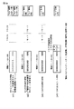
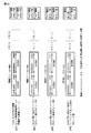
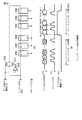
図3(a)に比較例に係るBCH符号に対する短縮化符号の方法を示す。
まず、図3の(a1)に示すように、前述のk0ビットより少ないkビットの情報ビットを準備する。次いで、(a2)に、l-bitの”0”を追加して、前述のk0ビットに相当するビット数に揃える。さらに、”0”bitを追加した情報系列をBCH符号化し、(a3)に示すように、検査ビットとなるパリティを付加したnビットの符号語を形成する。次いで、(a4)で示すように、符号化された符号語中のl-bitの”0”を取り除き、(n-l)ビットの符号語を不揮発性メモリに記憶する。このようにして、(n,k0)BCH符号から、((n-l),k(=k0-l))BCH短縮符号を形成している。ここで、情報ビットはBCH符号後でもそのまま情報ビットとして、検査ビットと分離している。この特徴はRS符号でも同様に存在する。
FIG. 3 (a) shows a shortened code method for the BCH code according to the comparative example.
First, as shown in (a1) of FIG. 3, k information bits fewer than the k0 bits are prepared. Next, l-bit “0” is added to (a2) to make it equal to the number of bits corresponding to the k0 bit described above. Further, the information sequence to which “0” bit is added is BCH-encoded to form an n-bit code word to which a parity to be a check bit is added as shown in (a3). Next, as indicated by (a4), the l-bit “0” in the encoded codeword is removed, and the (nl) -bit codeword is stored in the nonvolatile memory. In this way, a ((nl), k (= k0-l)) BCH shortened code is formed from the (n, k0) BCH code. Here, the information bits are separated from the check bits as information bits even after the BCH code. This feature is also present in the RS code.
しかしながら、上記のようにBCH短縮符号作成法やRS短縮符号作成法のみでは、”010”など符号の特定の連パターンに対して誤りに強い訂正方法ではなく、ランダムな単ビット、または、ランダムな一定数のバイトに対する誤り訂正方法である。よって、上記消去しきい値や書き込みしきい値が、隣接メモリセルが消去しきい値から書き込みしきい値になることにより容量結合によって上昇する問題や、隣接メモリセルのパターンによって、より誤書き込みが生じる問題に対して、よりこの問題の特徴を捉え、BCH符号やRS符号と組み合わせた場合に、より効果がある符号化の構成方法ではない。 However, only the BCH shortened code creation method and the RS shortened code creation method as described above are not correction methods that are resistant to errors with respect to a specific continuous pattern of codes such as “010”, but random single bits or random This is an error correction method for a certain number of bytes. Therefore, the above-described erase threshold value and write threshold value may increase due to capacitive coupling due to the adjacent memory cell changing from the erase threshold value to the write threshold value, and more erroneous writing may occur depending on the adjacent memory cell pattern. It is not a coding configuration method that is more effective when the characteristics of this problem are captured and combined with a BCH code or an RS code.
上記のように、比較例に係るデータ記憶システムは、消去しきい値や書き込みしきい値が容量結合によって変化し、隣接メモリセルのパターンによって誤書き込みが生じるランダマイズの問題に対して、ランダムな単ビット、または、ランダムな一定数のバイトに対する誤り訂正する構成である。その結果、例えば、”010”など符号の特定の連パターンに対して、より特徴を捉えた、誤りに強い訂正をすることができない点で不利である。 As described above, in the data storage system according to the comparative example, the random threshold is changed with respect to the randomization problem in which the erase threshold value and the write threshold value are changed by the capacitive coupling and the erroneous write is caused by the pattern of the adjacent memory cell. In this configuration, error correction is performed on a bit or a random fixed number of bytes. As a result, for example, it is disadvantageous in that a specific continuous pattern such as “010” cannot be subjected to error-proof correction that captures more features.
以下、最良と思われるいくつかの実施例1乃至実施例7について説明する。尚、この説明においては、全図にわたり共通の部分には共通の参照符号を付す。 Hereinafter, some examples 1 to 7 which are considered to be the best will be described. In this description, common parts are denoted by common reference symbols throughout the drawings.
[実施例1]
次に、図4乃至図9を用いて、この発明の実施例1に係るデータ記憶システムおよびその誤り訂正動作を説明する。
[Example 1]
Next, the data storage system and its error correction operation according to
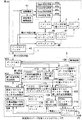
<1.構成例>
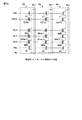
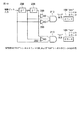
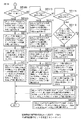
まず、図4を用いて、実施例1に係るデータ記憶システムの全体構成例を説明する。図4は、実施例1に係るデータ記憶システムのブロック図のレイアウトを示す。
<1. Configuration example>
First, an example of the overall configuration of the data storage system according to the first embodiment will be described with reference to FIG. FIG. 4 is a block diagram layout of the data storage system according to the first embodiment.
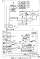
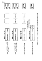
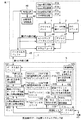
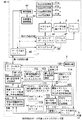
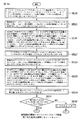
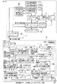
図示するように、本例に係るデータ記憶システムは、記憶装置7とメモリコントローラ5とにより構成される。
As shown in the figure, the data storage system according to this example includes a
記憶装置7として点線で囲った部分は、例えば、NAND型フラッシュメモリとして1つの半導体基板上に形成されている。メモリコントローラ5として点線で囲った部分は、いわゆるフラッシュメモリのコントローラに相当する回路構成を示したもので、通常、記憶装置7とは別の半導体基板上に形成された回路を示しているが、勿論同じ半導体基板に形成してもよい。このように、例えば、メモリコントローラ5と記憶装置7とが同一パッケージまたはボードやカード内に形成されることにより、データ記憶システムを形成している。
A portion surrounded by a dotted line as the
データ入出力バッファ45は、フラッシュメモリ コントローラ5のデータ入出力バッファ101と第1の内部I/O線により接続されている。
The data input /
ここで、本願すべての実施例に渡って、メモリセルはデータ破壊を伴わずに複数回読み出すことができるメモリセルとする。さらに、メモリセルブロック49の具体的構成については、以下に述べる。なお、フラッシュメモリの慣例に従い、消去状態の論理値を"1"、書きこみ状態の論理値を"0"とする。また、説明を簡単にするために、以下すべての実施例において、特に記述無い場合は2値のメモリセルのしきい値について記述するが、多値メモリセルの場合にも、勿論実施例の適用が可能である。この場合、メモリセルのしきい値が高い側から低い側の順で各データ保持のビットを表すのしきい値分布を配列した場合、任意の隣接する2つのしきい値分布a,b(aがbより低いしきい値分布とする)を考え、a以下のしきい値分布を”1”、b以上のしきい値分布を”0”と読み替えればよい。なお、NAND型フラッシュメモリでは、同一のデータ制御線に接続された消去メモリセルを一括消去し、NANDセルブロック49でも一括消去する方法を取られるため、消去しきい値の分布が2V以上6V以下と、0.1V以上1V以下の書き込みしきい値の分布幅よりも広くなる。このため、図5(a)の消去しきい値から書き込みしきい値へ隣接メモリセル(β、γ、ε)のいずれかのしきい値が変化した場合の当該メモリセル(α)のしきい値変化影響が最も大きくなるため、多値メモリセルにおいて、消去状態の論理値を"1"、それ以外のいずれかの書きこみ状態の論理値を"0"として読み替えるのが望ましい。
Here, in all the embodiments of the present application, the memory cell is a memory cell that can be read a plurality of times without data destruction. Further, a specific configuration of the
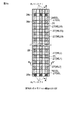
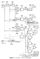
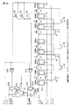
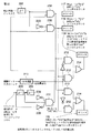
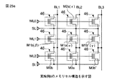
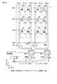
次に、図5a,図5bを用いて、メモリセルアレイの平面構成例について、説明する。図5a,図5bは、それぞれ、NANDセルブロック49の等価回路および平面図である。
Next, a planar configuration example of the memory cell array will be described with reference to FIGS. 5A and 5B. 5a and 5b are an equivalent circuit and a plan view of the
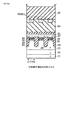
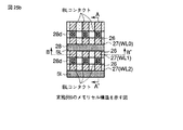
図5bでは、図5aのセルブロック49を3つ並列した構造を示している。特に、図5bでは、セル構造をわかりやすくするために、制御ゲート電極27よりも下の構造のみを示している。図5aでは、電荷蓄積電極26を有するMOSトランジスタからなる不揮発性メモリセルM0〜M31が直列に接続され、一端が選択トランジスタS1を介してBLと記してあるデータ転送線に接続されている。また他の一端は選択トランジスタS2を介してSLと記してある共通ソース線に接続されている。また、それぞれのトランジスタは、同一のp型ウェル23上に形成されている。また、それぞれのメモリセルM0〜M31の制御電極は、WL0〜WL31と記したデータ選択線に接続されている。また、データ転送線に沿った複数のメモリセルブロックから1つのメモリセルブロックを選択してデータ転送線に接続するため、選択トランジスタS1の制御電極はブロック選択線SSLに接続されている。さらに、選択トランジスタS2の制御電極はブロック選択線GSLに接続されており、いわゆるNAND型メモリセルブロック49(点線の領域)を形成している。ここで、本実施例では、選択ゲートの制御配線SSLおよびGSLがメモリセルエレメントの制御配線WL0〜WL31の電荷蓄積層26と同じ層の導電体によって、紙面左右方向に隣接するメモリセルで接続されて形成されている。ここで、メモリセルブロック49には、SSLおよびGSLのブロック選択線は少なくとも1本以上あればよく、データ選択線WL0〜WL31と同一方向に形成されることが、高密度化には望ましい。本実施例では、メモリセルブロック49に32=25個のメモリセルが接続されている例を示したが、データ転送線およびデータ選択線に接続するメモリセルの数は複数であればよく、割り切れる2n個もしくは、ダミーメモリセルをS2とWL0間、S1とWL31間に加えた2n+2個(nは正の整数)であることが多値メモリセルのブロックをアドレスデコードする上で望ましい。
FIG. 5b shows a structure in which three
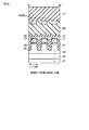
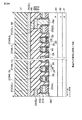
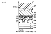
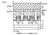
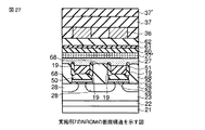
次に、図6a,図6bを用いて、メモリセルアレイの断面構成例について説明する。図6a,図6bは、図5b中の矢視B-B'およびA-A'方向断面図である。B-B'方向断面図は、メモリセル部断面図に相当する。図6aおよび図6bにおいて、例えば、ボロン不純物濃度が1014cm-3から1019cm-3の間のp型シリコン領域23に、例えば、3から15nmの厚さからなるシリコン酸化膜またはオキシナイトライド膜25,25SSL,25GSLから形成されたトンネルゲート絶縁膜を介して、例えばリンまたは砒素を1018cm-3から1021cm-3添加したポリシリコンからなる電荷蓄積層26,26SSL,26GSLが10nmから500nmの厚さで形成されている。これらは、例えば、シリコン酸化膜からなる素子分離絶縁膜24が形成されていない領域上に、p型シリコン領域23と自己整合的に形成されている。これは、例えば、半導体領域23に25,26を全面堆積した後、パターニングして半導体領域23に達するまで、半導体領域23を例えば0.05〜0.5umの深さエッチングし、絶縁膜24を埋め込むことで形成することができる。このように25および26を段差のない平面に全面形成できるので、より均一性の向上した特性の揃った製膜を行うことができる。
Next, a cross-sectional configuration example of the memory cell array will be described with reference to FIGS. 6A and 6B. 6a and 6b are cross-sectional views in the direction of arrows BB 'and AA' in FIG. 5b. The BB ′ direction cross-sectional view corresponds to the memory cell portion cross-sectional view. 6A and 6B, for example, a silicon oxide film or oxynite having a thickness of 3 to 15 nm is formed in the p-
この上に、例えば、厚さ5nmから30nmの間のシリコン酸化膜またはオキシナイトライド膜、またはシリコン酸化膜/シリコン窒化膜/シリコン酸化膜、または、アルミニウム、ハフニウム、ランタン、ジルコニウム元素を含む酸化膜とシリコン酸化膜,シリコン窒化膜からの積層膜からなるブロック絶縁膜50,50SSL,50GSLを介して、例えばリン、砒素、またはボロンを1017〜1021cm-3を不純物添加したポリシリコン、または、WSi(タングステンシリサイド)とポリシリコンとのスタック構造、または、Wとポリシリコンのスタック構造、または、NiSi,MoSi,TiSi,CoSiとポリシリコンのスタック構造からなる制御ゲート27が10nmから500nmの厚さで形成されている。この制御ゲート27は、図5bにおいて隣接するメモリセルブロックで接続されるように図5bにおいて紙面左右方向にブロック境界まで形成されており、データ選択線WL0〜WL31を形成している。なお、p型シリコン領域23は、n型シリコン領域22によってp型半導体基板21と独立に電圧印加できるようになっていることが、消去時の昇圧回路負荷を減らし消費電力を抑えるためには望ましい。本実施例のゲート形状では、半導体領域23の側壁が絶縁膜24で覆われているので、浮遊ゲート電極26を形成する前のエッチングで露出することがなく、ゲート電極26が半導体領域23よりも下に来ることを防ぐことができる。よって、半導体領域23と絶縁膜24との境界での、ゲート電界集中やしきい値低下した寄生トランジスタが生じにくい。さらに、電界集中に起因する書込みしきい値の低下現象、いわゆる、sidewalk現象が生じにくくなるため、より信頼性の高いトランジスタを形成することができる。
On this, for example, a silicon oxide film or an oxynitride film having a thickness of 5 nm to 30 nm, or a silicon oxide film / silicon nitride film / silicon oxide film, or an oxide film containing aluminum, hafnium, lanthanum, or zirconium element Polysilicon doped with 10 17 to 10 21 cm −3 of, for example, phosphorus, arsenic, or boron through
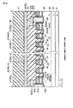
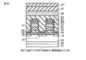
図6bに示すように、これらゲート電極の両側には、例えば5nmから200nmの厚さのシリコン窒化膜またはシリコン酸化膜からなる側壁絶縁膜43を挟んでソースまたはドレイン電極となるn型拡散層28が形成されている。これら拡散層28、電荷蓄積層26、および制御ゲート27により、電荷蓄積層26に蓄積された電荷量を情報量とする浮遊ゲート型EEPROMセルが形成されており、そのゲート長としては、0.5um以下0.01um以上とする。これらソースドレインn型拡散層28としては、例えばリンや砒素、アンチモンを表面濃度が1017cm-3から1021cm-3となるように深さ10nmから500nmの間で形成されている。さらに、これらn型拡散層28は隣接するメモリセル同士共有され、NAND接続が実現されている。また、図において、26SSL、さらに、26GSLは、それぞれSSLおよびGSLに相当するブロック選択線に接続されたゲート電極であり、前記浮遊ゲート型EEPROMの浮遊ゲート電極と同層で形成されている。ゲート電極26SSLおよび26GSLのゲート長は、メモリセルゲート電極のゲート長よりも長く、例えば、1um以下0.02um以上と形成することにより、ブロック選択時と非選択時のオンオフ比を大きく確保でき、誤書き込みや誤読み出しを防止できる。
As shown in FIG. 6b, on both sides of these gate electrodes, for example, an n-
また、27SSLの片側に形成されたソースまたはドレイン電極となるn型拡散層28dは、例えば、タングステンやタングステンシリサイド、チタン、チタンナイトライド、銅、またはアルミニウムからなるデータ転送線36(BL)とコンタクト31dを介して接続されている。ここで、データ転送線36(BL)は、隣接するメモリセルブロックで接続されるように図5(b)において紙面上下方向にブロック境界まで形成されている。一方、27(GSL) の片側に形成されたソースまたはドレイン電極となるn型拡散層28Sは、コンタクトコンタクト31sを介してソース線となるSLと接続されている。このソース線SLは、隣接するメモリセルブロックで接続されるように図5bにおいて紙面左右方向にブロック境界まで形成されている。勿論、n型拡散層28Sを紙面左右方向にブロック境界まで形成することにより、ソース線としてもよい。これらBLコンタクト、および、SLコンタクトとしては、例えばn型またはp型にドープされたポリシリコンやタングステン、およびタングステンシリサイド、Al、TiN、Tiなどが充填されて、導電体領域となっている。さらに、これらSLおよびBLと、前記トランジスタとの間は、例えばSiO2やSiNらなる層間膜68によって充填されている。さらに、このBL上部には、例えばSiO2、SiN、または、ポリイミドらなる絶縁膜保護層37や、図には示していないが、例えば、W,AlやCuからなる上部配線が形成されている。
Further, 27 n-
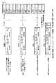
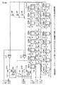
セルアレイ1は、図5aに示すように、不揮発性メモリセルを直列または並列接続したメモリセルブロック49を配列して構成される。このメモリセルアレイ1のデータ転送線のデータをセンスし、あるいは書き込みデータを保持するためにセンスアンプ回路46がデータ転送線選択トランジスタを介して設けられている。このセンスアンプ回路はデータレジスタを兼ねており、例えばフリップフロップ回路を主体として構成される。さらに、センスアンプ回路46は、データ入出力バッファ45に接続されている。これらの接続は、アドレスバッファ47からアドレス信号を受けるカラムデコーダ48の出力によって制御され、データ入出力バッファに与えられたデータをメモリセルアレイ1に書き込み、およびデータを図4の第1の内部I/O線へ読み出し可能となっている。メモリセルアレイ1に対して、メモリセルの選択を行うため、具体的にはデータ制御線WL0〜WL31、およびブロック選択ゲートSSL,GSLの制御をするために、ロウデコーダ3が設けられている。
As shown in FIG. 5a, the
基板電位制御回路42は、セルアレイ1が形成されるp型基板21(またはp型ウェル)の電位を制御するために設けられており、特に消去時に10V以上の消去電圧に昇圧されるように形成されることが望ましい。さらに、メモリセルアレイ1の選択されたメモリセルにデータ書き込みを行う際に、電源電圧よりも昇圧された書き込み電圧Vpgmを発生するための回路41aが形成されている。このVpgm発生回路41aとは別に、データ書き込み時に非選択のメモリセルに与えられる書き込み用中間電圧Vpassを発生するための回路41b、およびデータ読み出し時に非選択のメモリセルに与えられる読み出し用中間電圧Vread発生回路41cおよび選択セルのしきい値判定電圧を与える回路Vref発生回路1(41d)が設けられている。これらは、書き込み、消去、および読み出しの各状態で、必要な電圧出力がデータ制御線ドライバ2に加えられるように、制御回路40によって制御されている。Vpgmとしては、6V以上30V以下の電圧であり、Vpassは3V以上15V以下の電圧であり、Vreadとしては1V以上9V以下の電圧で、NAND型アレイの場合、書き込みしきい値上限よりも1V程度高い電圧が読み出し電流を十分確保しRead disturbを低下させるのには望ましい。さらに、Vref発生回路41としては、メモリセルの隣接する各しきい値、例えば、"1"と"0"のしきい値分布の分離しきい値の中間に設定する。また、データ制御線ドライバ2は、ロウデコーダ3の出力に従って、前記電圧出力を、書き込みまたは読み出しが必要なメモリセルの制御ゲートWL0〜WL15,SSL,GSLに印加するようにするスイッチ回路である。
The substrate
また、本出願のすべての実施例では、一連のシーケンスで読み出されるデータビット数が、mを自然数として、tを自然数として一連のシーケンスで読み出されるデータビット数が、[2m-1-t×(m-1)-1]より大きく(2m-t×m-1)以下である場合、少なくとも(2m-1)個以上のメモリセル49を図5(a)または図5(b)の紙面左右方向、つまりデータ選択線の延びる方向に並列に用意し、1ページとして用いる。また、本実施例の特徴上、2から6ビットの付加ビットを情報ビットに付加して効果を得るため、mとしては、少なくとも4以上であることが、本実施例によりアレイ面積増大を抑制するには必要であり、通常mはNANDフラッシュメモリでは、8以上20以下で用いられる。なお、1ページに属するメモリセルについては、例えば、1つのデータ選択線に共通に接続された複数のメモリセルとすることが、1度のデータ選択によって、複数のメモリセルを同時選択することができ望ましい。このようにメモリセルを準備することにより、例えば、Bose-Chaudhuri-Hocquenghem(BCH)符号を用いてセルアレイ1の一連のシーケンスで読み出されたtビットのビット誤りを検出し、その位置を求めることができる。RS符号の場合にも、1バイト中のデータは同時読み出しされるので、上記のようにメモリセル49を図5aまたは図5bの紙面左右方向、つまりデータ選択線の延びる方向に並列に用意し、1ページとして用いる。
Also, in all embodiments of the present application, the number of data bits read in a series of sequences is the number of data bits read in a series of sequences, where m is a natural number and t is a natural number, [2 m-1 -t × (m-1) -1] greater than (2 m -t × m-1 ) is less than or equal to at least the (2 m -1) or
さらに、センスアンプ46の入出力は、メモリセルの読み出しや書込み、および消去を制御する制御ロジック40に接続されている。制御回路40は、例えばデータバッファに与えられたデータをコマンド入力とし、メモリセルの読み出しや書込み、および消去を制御する。また、図では単純化のため示していないが、制御回路40より、センスアンプの動作を制御する制御信号やsel1、sel2制御信号が接続されている。なお、7で示す点線で囲った部分は、例えば、NAND型フラッシュメモリとして従来1つの半導体基板上に形成された記憶装置を示している。ここで、上記各構成ついては、例えば、特開2002-150783によって公知な回路ブロックを用いればよいので詳しい説明は省略する。
Further, the input / output of the
なお、以後、わかりやすくするために、慣例に因んで、符号化前のデータ列を情報ビット、符号化後に付加されるビットを検査ビットと呼ぶことにする。BCH符号、およびRS符号とも、元の情報ビットに検査ビットが付加されることにより、符号を形成する。従来技術で示したように、通常、検査ビットはその符号及び復号化の回路構成を単純にするため、情報ビットの後ろに付加される形となっている。 In the following, for the sake of clarity, the data string before encoding will be referred to as an information bit, and the bit added after encoding will be referred to as a check bit. Both the BCH code and the RS code form a code by adding a check bit to the original information bit. As shown in the prior art, the check bit is usually added after the information bit in order to simplify the circuit configuration of the code and decoding.
ここで、図4中の点線5で囲った部分は、いわゆるフラッシュメモリのコントローラに相当する回路を示したもので、通常、記憶装置7とは別の半導体基板上に形成された回路を示しているが、勿論同じ半導体基板に形成してもよい。例えば、5と7とが同一パッケージまたはボードやカード内に形成されることにより、データ記憶システムを形成している。データ入出力バッファ45はフラッシュメモリ コントローラ5のデータ入出力バッファ101と第1の内部I/O線により接続されている。
Here, a portion surrounded by a dotted
一方、外部入出力(I/O)は別のデータ入力バッファ111に接続され、フラッシュメモリの書き込み/消去/読み出しのアドレスおよびデータ制御情報を入力する。さらに、フラッシュメモリ コントローラー5にはコントローラ制御回路120によって、2つのデータ入出力バッファ101,111の入出力のデータ入出力の制御を行っている。データ入出力バッファ111からは、外部I/Oを通じて入力された情報ビットが、符号出現確率平均化第一符号化回路106に入力されている。ここで、106に入力される情報ビットのビット数をk0ビットとする。この符号出現確率平均化第一符号化回路106は、例えば、入力データの”0”と”1”の出る確率をほぼ均等に分布するようにするためのものであり、無くてもよいが、有れば望ましい回路ブロックである。この106としては、例えば、周期符号発生回路や、特に、kビットより短いa1ビットの周期を持つM系列(Maximum length code)発生回路を平均化ビットマスク発生回路110に用いればよい。これにより発生したM系列符号は、M1周期で”0”と”1”のビットが分散して配置され、1周期で”0”,”1”が等しい確率で生成される特徴を有する。よって、情報ビットをa1ビットごとに順に区切り、発生したM系列のa1の各ビットと排他的論理和を取り、104回路へ出力し、かつ、例えば、WL毎やa1のブロックごとに適当な増分をもって、周期開始位置を変化させる。または周期開始位置ではなく、a2ビットの長さの第二のM系列符号を発生させ、さらに、情報ビットをa1ビットごとに順に区切り、発生したM系列のa1の各ビットと排他的論理和を取った後に、情報ビットをa2ビットごとに順に区切り、発生した第二のM系列のa2の各ビットと排他的論理和を取る。具体的例としては、2ビットの線形フィードバックレジスタ(LFSR:Linear Feedback Shift Register)の原始多項式はx+1であるから、2ビット目(x)と1ビット目(1)の排他的論理和を次の符号の1ビット目とし、2ビット目を1ビット目からシフトにより得ることにより、”10”,”01”,”11”,の22-1=3状態を得ることができる。これに0ベクトルである” 00”を足した4状態がM系列となるから、情報ビットを2ビット毎に順に区切り、”10 01 11 00 10 01 11 00 ….”と順に各データ順に排他的論理和を取ればよい。
On the other hand, an external input / output (I / O) is connected to another
このようにすることにより、全部”0”や全部”1”の入力の情報ビットでも、WL間でも”0”や”1”が適宜分散した第一符号化された情報ビットが104に伝達される。これにより、ランダムに外部I/Oから情報データを与えた場合でも、情報ビットが”0”,”1”で等しい確率P=0.5で104に入力され、メモリセルの隣接メモリセル状態の均一化することができる。なお、勿論、平均化ビットマスク発生回路110は、復号回路107でも同じM系列回路、または第二のM系列回路を共有化することにより、復号回路と同じく発生したM系列のa1,a2の各ビットと排他的論理和を取ることにより、正しく復号化することができる。
By doing this, the first encoded information bits in which all “0” and all “1” input information bits and “0” and “1” are appropriately distributed between WLs are transmitted to 104. The As a result, even when information data is randomly given from the external I / O, the information bits are input to 104 with the probability P = 0.5 which is equal to “0” and “1”, and the memory cells adjacent to each other are made uniform. can do. Of course, the averaged bit
さらに、104で入力された、”0”,”1”で平均化された情報ビットは、隣接メモリセルディスターブ低減第二符号変換回路104にて、隣接メモリセルによるディスターブが低減した情報ビットとフラグが付加されたビット列となり、誤り訂正符号発生回路102に入力される。ここで、102は、例えば、一般に知られているBCH符号発生回路またはRS符号発生回路を用いればよい。例えば、本発明者らが特開2005-243183にて開示したBCH符号化回路を用いれば実現できるのでここでは省略する。これにより、102より誤り訂正符号出力がデータバッファ101を通じて、不揮発性半導体記憶素子7に記憶される。
Further, the information bits averaged by “0” and “1” input at 104 are converted into information bits and flags in which the disturbance by the adjacent memory cells is reduced by the adjacent memory cell disturb reduction second
なお、本発明は、物理的に隣接したメモリセル間の容量干渉、または、誤書き込み問題を低減する符号化を行う発明なので、不揮発性半導体記憶装置7に与えられる隣接した時系列の情報ビットは、ウェル境界、ソースシャント領域などを除きおおむね物理的に隣接したメモリセルに書き込まれるものとする。適切な物理―論理マッピングを行えばこのような符号化が可能であることは言うまでもない。
Since the present invention performs encoding to reduce the capacity interference between physically adjacent memory cells or the erroneous writing problem, adjacent time-series information bits given to the nonvolatile
一方、不揮発性メモリ7から読み出された誤りを含む可能性のある符号列は、データバッファ101を通じて、誤り訂正符号を復号する回路103に入力され、符号誤り訂正され、隣接メモリセルによるディスターブが低減した情報ビットとフラグが付加されたビット列となる。この103については、一般に知られているBCH符号復号回路またはRS符号復号回路を用いればよい。BCH復号回路については、例えば、本発明者らが特開2005-243183にて開示したBCH符号化回路を用いれば実現できるのでここでは省略する。同様にRS符号も多元、2m元(mは整数)のBCH符号の一種なので、復号回路が同様に形成できることは公知であり明らかである。
On the other hand, a code string that may contain an error read from the
ついで、隣接メモリセルによるディスターブが低減した情報ビットとフラグが付加されたビット列は、隣接メモリセルディスターブ低減第二符号逆変換回路105に入力され、第二符号復号化回路105によって、第一符号を施した情報ビットに復号される。さらに、この第一符号を施した情報ビットを第一符号復号化回路107に入力することにより、元の情報ビットが復号される。この情報ビットの出力が、データ入出力バッファ111を通じて外部I/Oでデータが出力される。
Next, the information bit in which the disturbance by the adjacent memory cell is reduced and the bit string to which the flag is added are input to the adjacent memory cell disturb reduction second code
なお、この第一符号復号化回路107は、前述のように、110で発生されたのと106回路で用いたものと同じM系列と排他的論理和をとることにより、符号化と復号化でM系列と排他的論理和を2回とることとなり、元の情報ビットが復元できることは明らかである。
Note that, as described above, the first
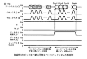
図9に、例として、様々な情報ビットパターンでの104回路の入力、および途中シーケンスの状態、更に、出力例を示す。”....“の示す箇所はその右側の4ビットのパターンを周期的に繰り返されるものとする。一般に、入力情報ビットがkビットである場合、106回路で出現確率は平均化されてはいるが、すべての情報ビットが”0”,”1”に任意に変化し取りうる全状態を考える必要がある。すなわち、106で符号化および107で復号化できる以上、kビットの情報ビットでは、2k個の状態が存在し、2つの隣接ワード線間で2k×2k個すべての組み合わせが存在し、その出現確率は106回路によりすべての状態でほぼ平均化されている。なお、以下すべての実施例内で、誤り訂正符号発生回路102、隣接メモリセルディスターブ低減第二符号変換回路104、符号出現確率平均化第一符号化回路106、および、誤り訂正符号復号回路103、隣接メモリセルディスターブ低減第二符号逆変換回路105、第一符号復号化回路107、平均化ビットマスク発生回路110、”01010101....0101”の排他的論理和をとった後の”010”カウンタ112、”10101010....1010”の排他的論理和をとった後の”010”カウンタ113、”010”シンボルカウンタ108、”101”シンボルカウンタ109、カウンタ116、カウンタ117,カウンタ118,カウンタ119、情報ビットの並べ替えを行うページバッファ114、1つソース線側のデータを記憶ページバッファ115は、ハードウェア回路で実施してもよいし、計算処理時間が問題なければいわゆるソフトウェアやファームウェアやそれらの組み合わせにて実現しても勿論良い。また、以降のすべての実施例において、簡単のため情報ビット数kビットが偶数、例えば、2で割り切れる場合や、4で割り切れる場合を示している。なお、割り切れないビット数の場合は、例えば、4の倍数となるまで”1”を付加することにより情報ビットを拡大し、割り切れるように符号化する方法を用いればよい。例えば、情報ビットが5ビットの”10101”の場合、これを8ビットの”10101111”とすれば、2でも4でも割り切れる符号となることは明白である。なお、付加する符号としては、付加符号による”010”パターンの新たな発生を防ぐために、”0”よりは”1”の方が望ましい。
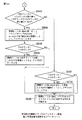
FIG. 9 shows, as an example, the input of 104 circuits in various information bit patterns, the state of an intermediate sequence, and an output example. "...." position indicated by shall be repeated pattern of 4 bits to the right periodically. In general, when the input information bits are k bits, the appearance probability is averaged in 106 circuits, but it is necessary to consider all states in which all information bits can be arbitrarily changed to “0” and “1”. There is. That is, as long as it can be encoded at 106 and decoded at 107, there are 2 k states for k information bits, and all 2 k × 2 k combinations between two adjacent word lines, The appearance probability is almost averaged in all states by 106 circuits. In all the following embodiments, the error correction
<2.誤り訂正符号/複号動作>
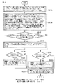
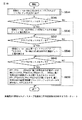
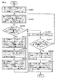
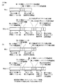
次に、図7乃至図9を用いて、本実施例1に係るデータ記憶システムの誤り訂正符号/復号動作について説明する。図7に104の具体的シーケンスを示す。この説明では、図7または図8のシーケンスに則して説明する。
<2. Error correction code / decoding operation>
Next, an error correction encoding / decoding operation of the data storage system according to the first embodiment will be described with reference to FIGS. FIG. 7 shows a
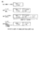
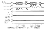
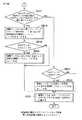
第2符号変換回路104では、まず、SE1において、情報ビットの中の”010”の3bit連続したシンボルの発生数を数える”010”シンボルカウンタ108と、情報ビットの中の”101”の3bit連続したシンボルの発生数を数える”101”シンボルカウンタ109とをリセットし、符号化の状態を表すフラグ1及びフラグ2をリセットする。以後、例えば、”abc”シンボルとは、情報ビットまたは符号内で、”abc”で示される連続した3bitを示すことにする。
In the second
ついで、SE2において、kビットの情報ビット中の”010”の連続ビットの個数をカウントし”010”シンボルカウンタ108に記憶する。また、kビットの情報ビット中の”101”の連続ビットの個数をカウントし”101”シンボルカウンタ109に記憶する。
Next, in SE2, the number of consecutive bits “010” in k information bits is counted and stored in the “010”
例えば、”010”検出回路は、図10のように、情報ビットの初めから、情報ビットと同期したクロックでシフトレジスタに入力し、”010”検出回路を組み合わせて、カウンタで数えることにより容易に実現することができる。図10において、208のZ-1は1ビットの1単位時間遅延素子を示し、209はインバータ、210に3入力ANDゲートを示している。また、情報ビットは情報ビット入力より一連の情報ビットを順に時系列にて入力するものとする。”010”が順に入力された単位時間において、”010”最後の”0”が入力された単位時間で、”010”出力が”L”から”H”となり、他の場合には”L”となる。よって、この”010”出力を情報ビット入力の単位時間と同期させ、例えば、前記単位時間で”010”出力の論理値が安定したところでトリガしてカウントすることにより、情報ビットの”010”の数をカウントすることができる。”101”のカウントも同様に行うことができ、例えば、図10のカウンタは一般に知られるバイナリカウンタで構成すればよいので、ここではカウンタの詳細は省略する。なお、本例の208のZ-1で表記される1ビットの1単位時間遅延素子としては、例えば、D型フリップフロップやラッチ回路を用い、特に、クロック入力が"L"(ここでは便宜的に0[V]とする)から"H"(ここでは便宜的にVccとする)に立ち上がる瞬間に出力が確定し、それ以後はクロックが"H"のままでも"L"のままでも"H"から"L"へ変化しても出力は変化しないエッジトリガー(edge trigger)型のフリップフロップとすれば容易に実現できる。 For example, as shown in FIG. 10, the “010” detection circuit can be easily input from the beginning of the information bit to the shift register using a clock synchronized with the information bit, combined with the “010” detection circuit, and counted by the counter. Can be realized. In FIG. 10, Z- 1 in 208 indicates a 1-bit 1-unit time delay element, 209 indicates an inverter, and 210 indicates a 3-input AND gate. In addition, as information bits, a series of information bits are sequentially input in time series from information bit input. In the unit time in which “010” is input in order, the “010” output is changed from “L” to “H” in the unit time in which “010” is input at the last “0”. In other cases, “L” It becomes. Therefore, this “010” output is synchronized with the unit time of the information bit input. For example, by triggering and counting when the logical value of the “010” output is stable in the unit time, the information bit “010” is output. The number can be counted. The count of “101” can be performed in the same manner. For example, the counter of FIG. 10 may be configured by a generally known binary counter, and therefore details of the counter are omitted here. As the 1-bit 1-unit time delay element represented by Z- 1 in 208 in this example, for example, a D-type flip-flop or a latch circuit is used, and in particular, the clock input is “L” (here, for convenience). The output is fixed at the moment when it rises from "0 [V]" to "H" (here, Vcc for convenience), and after that the clock remains "H" or "L". This can be easily realized by using an edge trigger type flip-flop in which the output does not change even if it changes from “L” to “L”.
ついで、SE3において、108の”010”カウンタの値が第一のしきい値より大きいか判断する。ここで、第一のしきい値より大きい場合、SE4にて、情報ビットと第一ビットマスクパターン”01010101....0101”(”01”をkビット分繰り返し発生させたもの)との排他的論理和をとるシーケンスを行い、情報ビットと置き換えを行い、フラグ1をセットする。この第一ビットマスクパターンは、”10”をkビット分繰り返し発生させた、”10101010....1010”を用いても良い。また、第一のしきい値は、情報ビットの中に、図9(a1)および図9(c1)の最も”010”の多い個数の(k/2)-1個の半分を考え、k個が2か4で割り切れない場合も考慮して、{(k/4)を整数に切り上げた値}-1とするのが、”010”の符号の出現数の上限を一定値に抑制するのに望ましい。
Next, in SE3, it is determined whether the value of the “010”
さらに、SE4を実施した場合には、SE5において、情報ビットの中の”010”の3bit連続したシンボルの発生数を数える”010”シンボルカウンタ108と、情報ビットの中の”101”の3bit連続したシンボルの発生数を数える”101”シンボルカウンタ109とをリセットし、符号化の状態を表すフラグ1及びフラグ2をリセットする。さらに、SE6にて、kビットの情報ビット中の”010”の連続ビットの個数をカウントし”010”シンボルカウンタ108に記憶する。また、kビットの情報ビット中の”101”の連続ビットの個数をカウントし”101”シンボルカウンタ108に記憶する。
In addition, when SE4 is implemented, in SE5, “010”
ついで、SE3のNoと判断した分岐と合流後、SE7にて、”010”シンボルカウンタ108の値と、”101”シンボルカウンタ109の値より大きいか判断を行う。ここで、”010”シンボルカウンタ108の値が”101”シンボルカウンタ109の値より大きい場合には、SE8にて、kビットの情報ビットを全部ビット反転、すなわち”0”ビットを”1”ビット、”1”ビットを”0”ビットに変化させ、フラグ2をセットする。次いで、SE7のNoと判断した分岐と合流後、SE9にて情報ビットにフラグ1およびフラグ2に相当する符号を付加する。
Next, after joining the branch determined to be No in SE3, it is determined in SE7 whether the value of the “010”
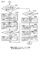
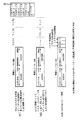
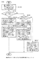
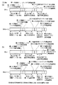
(復号化回路105のシーケンス)
ここで、図8に第二符号の復号化回路105の具体的シーケンスを示す。105では、まず、SE10において、情報ビットに付加されたフラグ1およびフラグ2に相当する情報を、例えば、レジスタや一時メモリに記憶する。ついで、SE11にて、フラグ2がセットされているか判断後、フラグ2がセットされている場合には、SE12にて、kビットの情報ビットを全部ビット反転、すなわち”0”ビットを”1”ビット、”1”ビットを”0”ビットに変化させ、情報ビットと置き換える。ついで、SE11のNoと判断した分岐と合流後、SE13にて、フラグ1がセットされているか判断する。SE13でYes、すなわちフラグ1がセットされている場合、情報ビットと第一ビットマスクパターン”01010101....0101”(”01”をkビット分繰り返し発生させたもの)との排他的論理和をとるシーケンスを行い、情報ビットと置き換えを行う。この第一ビットマスクパターンは、104の符号化の際”10”をkビット分繰り返し発生させた、”10101010....1010”を用いた場合には、同じ”1010101010....1010”マスクビットを用いれば良い。
(
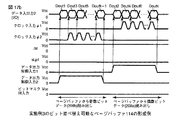
Here, FIG. 8 shows a specific sequence of the
ここで、比較例の図2中の(iii)および(iv)で示した、隣接メモリセルのしきい値電圧上昇による消去しきい値の増大する問題が生じるパターンは、当該メモリセル(α)が消去状態、BL方向に隣接するセル(β、γ)が書き込み状態となるので、ビット列としては”010”に相当する。ここで、図9(a1)から(a4)で示すように、104のシーケンスがない比較例の構成では、”01010101....0101”のkビットの系列では、”010”が[(k/2)-1]個含まれ、この箇所分、隣接メモリセルのしきい値電圧上昇による消去しきい値の増大する問題が大きな確率で生じる。例えば、1つのメモリセルαが図2の書き込みしきい値(v)との重なりが生じたり、読み出しレベルが書き込みしきい値とする判断するしきい値が超え、消去ビットが書き込みビットと誤認識され不良する確率p0とすると、p0が十分1より小さいとして、[(k/2)-1]×p0の不良が生じたりする。なお、この図9(a1)と図9(c1)が比較例で”010”が最も生じる最悪パターンである。一方、本実施例の104のシーケンスを用いることにより、図9(a1)のように”010”の個数は104に入力されるデータパターンでは、[(k/2)-1]個存在するが、SE3のシーケンスを行うことにより、SE7の前までで”010”の個数は{(k/4)を整数に切り上げた値}-1以下に抑えることができる。なぜなら、SE3の分岐で、SE4へ進んだ場合、”010”の数は{(k/4)を整数に切り上げた値}-1より多く、最悪、”010”が最も稠密に並んだ場合においても、”01010101....01010”が(k/2)+1ビット以上連続したビットで占めることになる。よって、”010”以外のパターン、特に、”000”の存在するビット数は高々(k/2)ビットより少ない。よって、情報ビットを”01010101....0101”のマスクにて排他的論理和とった場合、"000"ビットが”010”の連続ビットに反転し”010”が増える箇所は、高々{(k/4)を整数に切り上げた値}-1以下しか増加しない。
Here, as shown in (iii) and (iv) of FIG. 2 of the comparative example, the pattern in which the problem that the erase threshold value increases due to the threshold voltage rise of the adjacent memory cell is the memory cell (α) Is in the erased state, and the cells (β, γ) adjacent in the BL direction are in the written state, so that the bit string corresponds to “010”. Here, as shown in FIGS. 9 (a1) to (a4), in the configuration of the comparative example without 104 sequences, in the k-bit sequence “01010101 .... 0101”, “010” is [(k / 2) -1] is included, and the problem that the erase threshold value increases due to the threshold voltage increase of the adjacent memory cell occurs with a large probability. For example, one memory cell α is overlapped with the write threshold value (v) in FIG. 2 or the threshold for determining the read level as the write threshold is exceeded, and the erase bit is erroneously recognized as the write bit. Assuming that the failure probability is p0, it is assumed that p0 is sufficiently smaller than 1, and a failure of [(k / 2) -1] × p0 occurs. FIG. 9 (a1) and FIG. 9 (c1) are the worst patterns in which “010” occurs most in the comparative example. On the other hand, by using the
一方、また、”010”は”01010101....0101”とのマスクにて排他的論理和とった場合には、”010”のビットの開始位置によって、”010”か”101”のいずれかのパターンと排他的論理和をとることになる。これらは、それぞれ、”000”、”111”と変換されるため、いずれも問題となる”010”のパターンは全体として{(k/4)を整数に切り上げた値}-1以下に減少することになる。勿論、情報ビットとのマスクとして”01”が繰り返された”01010101....0101”を用いることが、最も情報ビットの”010”のパターンを減少させるのに有効である。しかしながら、例えば、ウェルコンタクトやソースシャントコンタクト部分では、ダミーメモリセルがビット線方向に隣接して、情報記憶するメモリセルと、ウェルコンタクトやソースシャントコンタクト部分の間に、例えば1つから16つ形成されることがある。例えば、このダミーセル部分の構成について本発明者は、特開2007-221084にて詳しく述べているので、ここでは省略する。この場合、ダミーメモリセルでは、情報データに応じメモリセルの書き込みまたは消去が行われないため、ダミーメモリセルに隣接する情報記憶するセル列の端は”0”でも”1”でも、比較例で述べた隣接メモリセルによるしきい値変化の問題が生じにくい特徴を有する。よって、例えば、ウェルコンタクトやソースシャントコンタクトなどメモリセルのアレイ区切りごとに適宜”01”の繰り返しである”01010101....0101”または、“10”の繰り返しである”10101010....1010”のどちらでも切り替えて用いても勿論構わないし、メモリセルの上記アレイ区切りごとに情報ビットを区切った情報ビットの部分列とし、それぞれの部分列について”010”および”101”の個数を数えて、それぞれの部分列に対応する104に示したフラグ1,2を付して、より”010”の出現する確率を減少させても勿論良い。これは後述の実施例のどの実施例に適用してもよい。上記に示したように、”010”の個数がしきい値1より多い場合、”01010101....0101”または ”10101010....1010”で排他的論理和をとることにより、情報ビット中の”010”の個数を最悪値で比較例[(k/2)-1]の約半分である、{(k/4)を整数に切り上げた値}-1以下に減少できることは、本発明者が見出した第一の特有な特徴である。以上より、図7のシーケンスによって、情報ビット中の”010”の数を比較例の最悪値の[(k/2)-1]より、{(k/4)を整数に切り上げた値}-1以下に抑えることができる。勿論、”01010101....0101”とのビットマスクにて排他的論理和とっているので、符号化後に同じビットマスクにて排他的論理和をとることにより、元の情報を復元できる。さらに、誤り訂正シンボル数をtとすると、BCH符号やRS符号の復号化には、tのほぼ2乗以上に比例する情報処理量が増加し、復号高速化の問題となる。これにに比べ、第二符号化回路104、および第二符号復号化回路105では、高々符号化および復号化では、情報ビットが長くなっても情報ビット長の1乗程度しか増加しない情報処理量しか必要とせず、tが3以上の場合、復号化より情報処理量がはるかに少ないBCH符号やRS符号の符号化に必要なLFSRのシフトの情報処理量と同程度である。よって、例えば、1000bitより長い符号長の場合でも第二符号への変換や逆変換には十分短い時間で変換することができる。
On the other hand, if “010” is exclusive ORed with the mask “01010101 .... 0101”, either “010” or “101” will be selected depending on the start position of the “010” bit. This pattern is exclusive-ORed with that pattern. Since these are converted to “000” and “111”, respectively, the pattern of “010”, which is a problem, is reduced to {-1 (rounded up to (k / 4))}-1 or less as a whole. It will be. Of course, using “01010101... 0101” in which “01” is repeated as a mask with information bits is most effective in reducing the pattern of information bits “010”. However, for example, in the well contact or source shunt contact portion, dummy memory cells are adjacent to each other in the bit line direction, for example, 1 to 16 are formed between the memory cell for storing information and the well contact or source shunt contact portion. May be. For example, the present inventor has described the configuration of the dummy cell portion in detail in Japanese Patent Application Laid-Open No. 2007-221084, and is omitted here. In this case, since the memory cell is not written or erased in accordance with the information data in the dummy memory cell, the end of the cell column storing information adjacent to the dummy memory cell may be “0” or “1”. It has a feature that the problem of threshold change due to the adjacent memory cell described above hardly occurs. Therefore, for example, “01010101 .... 0101”, which is a repetition of “01”, or “10101010 .... 1010, which is a repetition of“ 10 ”, as appropriate for each memory cell array partition such as a well contact or a source shunt contact. Of course, it may be used by switching either of them, and the information bits are divided into substrings for each array delimiter of the memory cell, and the number of “010” and “101” is counted for each substring. Of course, the
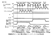
図9(a1),(b1),(c1),(d1),(e1)に様々な情報ビットの入力例と、右端に”010”の個数と、”101”の個数を示す。ついで、図9(a2),(b2),(c2),(d2)に104内でSE3後の状態を示す。図9(a)、図9(c)では、”010”の数がしきい値1の{(k/4)を整数に切り上げた値}-1より大きく、SE3の分岐はYesとなり、SE4にて、フラグ1をセットし、図9(a)および図9(c)では、SE3の”010”の数がしきい値1以下となり、SE3の分岐はNoとなる。ついで、図9(a3),(b3),(c3),(d3)に104にて、SE9前の状態を示す。
FIGS. 9 (a1), (b1), (c1), (d1), and (e1) show examples of input of various information bits, the number of “010” and the number of “101” at the right end. Next, FIGS. 9 (a2), (b2), (c2), and (d2) show the state after SE3 in 104. FIG. In FIG. 9 (a) and FIG. 9 (c), the number of “010” is larger than the threshold 1 {value obtained by rounding up (k / 4) to an integer} −1, the branch of SE3 becomes Yes, and SE4 Then,
ここで、比較例の図2の(iii)および(iv)で示した、隣接メモリセルのしきい値電圧上昇による消去しきい値の増大する問題が生じるパターンは、当該メモリセル(α)が消去状態、BL方向に隣接するセル(β、γ)が書き込み状態となるので、ビット列としては”010”に相当し、ビット反転した”101”では、前記比較例の問題は生じない。また、問題となる”010”となるビット列は、”101”をビット反転したものであり、SE7で”010”の個数と”101”の個数とを比較することにより、この2種類のパターンの入れ替えのみで効果的に”010”の出現個数を減らすことができる。ここで、図9(d1)から(d4)で、SE8でフラグ2がセットされる例を示す。図9(d1)で示すように、”0100”を繰り返す情報ビットのパターンでは、(k/4)個の”010”の個数と、0個の”101”の個数が存在する。よって、SE3にてNo側の分岐をした後、SE7にて、”010”の個数をカウントした108のカウンタが”101”の個数のカウントをした109のカウンタよりも多いか判断し、Yesの分岐に進む。ついで、SE8にて全ビット反転を行うことにより、0個の”010”の個数と、(k/4)個の”101”の個数になるので、結局、”010”の個数を減らすことができる。勿論、あらかじめ、SE7にて”010”の個数をカウントした108のカウンタが”101”の個数のカウントをした109のカウンタよりも多いか判定しており、Noの場合にはビット反転を行わないので、この場合には、”010”の個数が増加することはない。
Here, as shown in FIGS. 2 (iii) and (iv) of the comparative example, the pattern in which the problem that the erase threshold value increases due to the threshold voltage rise of the adjacent memory cell is the memory cell (α) Since the cells (β, γ) adjacent in the erased state and the BL direction are in the written state, the bit string corresponds to “010”, and the bit-inverted “101” does not cause the problem of the comparative example. The bit string that becomes “010” in question is a bit-inverted version of “101”. By comparing the number of “010” with the number of “101” in SE7, The number of occurrences of “010” can be effectively reduced only by replacement. Here, an example in which the
以上のように、本実施例1の104のSE7およびSE8のシーケンスを用いることにより、SE7前で既に情報ビット中の”010”の数を{(k/4)を整数に切り上げた値}-1以下に抑えているので、SE8の前までで”010”の個数は{(k/4)を整数に切り上げた値}-1以下で、かつ、より”010”の生じる情報ビットを効果的により”010”が生じないビットに変換することができる。 As described above, by using the sequence of SE7 and SE8 of 104 of the first embodiment, {the value obtained by rounding up the number of “010” in the information bits before SE7 {round up (k / 4) to an integer} — Since it is kept to 1 or less, the number of "010" before SE8 is {value obtained by rounding up (k / 4) to an integer} -1 or less, and more effective information bits that produce "010" are effective. Therefore, it can be converted into a bit in which “010” does not occur.
なぜなら、SE3からSE6までのシーケンスで、各情報ビットはマスクパターンとの排他的論理和をとっているのみなので、既に106回路にて、各情報ビットの”0”が出る確率と”1”が出る確率がほぼ等しく平均化された場合、104に入力された情報ビット各情報ビットの”0”が出る確率と”1”が出る確率は等しい。よって、SE7の分岐で、情報ビットの2のkべき乗のすべての組み合わせを考える場合、カウンタ108がカウンタ109より大きくなる確率は、カウンタ108がカウンタ109より小さくなる確率と同じとなる。よって、SE7およびSE8を行うことによりカウンタ108がカウンタ109と一致する情報ビット列、例えば、”01010111111111111....1111”のような場合を除いた、残りの半分の場合の”010”の生じる確率を低減し、より少ない”010”の生じる情報ビットを効果的に実現できる。
Because, in the sequence from SE3 to SE6, each information bit is only exclusive-ORed with the mask pattern, so the probability that “0” of each information bit is already output and “1” is already in 106 circuits. When the probability of exiting is approximately equalized, the probability that “0” is output for each information bit input to 104 is equal to the probability of “1” being output. Therefore, when considering all combinations of 2 to the power of 2 of information bits at the branch of SE7, the probability that the
なお、フラグ1およびフラグ2を情報ビットに付加する方法として、各フラグを2ビットの連続するデータとして情報ビットに付加する方法を示した。この方法は、フラグ1,2がどの状態でも”010”の状態が生じないように選択しているが、勿論、これ以外の符号化、例えば、フラグ1を同一2ビット割り当て、フラグ2を1ビットに割り当てる方法でも良い。これは、図9にて、フラグ1,2に対応するビットがaabb(a,bはそれぞれフラグ1,2に相当する”0”,”1”の状態)となっているが、bbaa、aabやbbaなど順番を入れ替えたものをフラグに対応するビットとして付加してもよい。勿論、このフラグに相当するビットは、情報ビットの前後に付加するのではなく、例えば、情報ビットを2つに分け、bbaaのようにして情報ビットの中に埋め込んでもよい。勿論情報ビットを3つに分け、bb,aaをそれぞれ3つの情報ビットの間に入るように埋め込んでもよい。
As a method of adding the
また、誤り訂正符号化した後に、検査ビット(パリティ)ビットを数個に分割し、aa、bbのように2個以上の同じビットからなるフラグを検査ビットで挟むように並べ替え(インタリーブ)してもよい。このようにすれば、2個以上の同じビットからなるフラグに接するビットは”010”パターンになり得ないため、より、検査ビット部分の”010”パターンの生じる可能性を減少できる。 Also, after error correction coding, the check bits (parity) bits are divided into several pieces and rearranged (interleaved) so that two or more identical bits such as aa and bb are sandwiched between check bits. May be. In this way, since the bit contacting the flag composed of two or more same bits cannot be a “010” pattern, the possibility of the occurrence of the “010” pattern in the check bit portion can be further reduced.
また、図9(e1)-(e4)に本実施例で”010”が生じる最悪パターン例を示す。図9(e1)に示すように、(k/2)ビットを”10”ビット繰り返したものとし、(k/2)ビットを”00”と繰り返したものとした場合、”010”パターンの個数は(k/4)-1個、”101”パターンの個数も(k/4)-1個となる。よって、この場合、図7のシーケンスでは、フラグ1はリセット、フラグ2もリセットのままではあるが、SE4、SE8、およびSE4とSE8の両方のシーケンスを仮に行った場合を図9(e2)、(e3)、(e4)で示す。この場合、いずれも、”010”パターンの個数は(k/4)個か(k/4)-1個、”101”パターンの個数も(k/4)個か(k/4)-1個となり、これより、仮にSE4またはSE8を行った場合でも、”010”パターンの選択個数は(k/4)-1となり、これがkビットの情報ビット”010”パターンの最悪パターンの1例となる。なお、この最悪パターンは、実施例3で述べる方法で、さらに改善できる。
FIGS. 9 (e1) to (e4) show examples of worst patterns in which “010” occurs in this embodiment. As shown in Fig. 9 (e1), if (k / 2) bits are repeated "10" bits and (k / 2) bits are repeated "00", the number of "010" patterns Is (k / 4) -1 and the number of "101" patterns is also (k / 4) -1. Therefore, in this case, in the sequence of FIG. 7, the
尚、本実施例1は、後述する実施例2,3に比べ、カウンタ112,113の追加が必要なく、より回路規模を減少させ、小さな面積の回路で構成できる利点を有する。
The first embodiment has the advantage that it is not necessary to add
<3.この実施例に係る効果>
この実施例に係るデータ記憶システムによれば、少なくとも下記(1)乃至(2)の効果が得られる。
<3. Effects according to this embodiment>
According to the data storage system of this embodiment, at least the following effects (1) to (2) can be obtained.
(1)例えば、”010”など符号の特定の連パターンに対して、より特徴を捉えた、誤り訂正に有利である。 (1) For example, it is advantageous for error correction that captures more features with respect to a specific continuous pattern of codes such as “010”.
上記のように、本実施例では、kビットの情報ビットに対して、高々3ビットから4ビット、情報としては高々2bitを付加するだけで、効果的に”010”の出現する最悪状態数を[(k/2)-1]から{(k/4)を整数に切り上げた値}-1以下、つまり約半分以下に抑制できる。 As described above, in this embodiment, the worst state number in which “010” appears effectively can be obtained by adding at most 3 to 4 bits and at most 2 bits as information to k information bits. [(k / 2) -1] to {(k / 4) rounded up to an integer)}-1 or less, that is, about half or less.
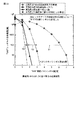
例えば、図29中の矢印Y1に示すように、”010”のシンボル数が100個程度の場合に、比較例と比べ、”010”の出現する最悪状態数を半分以下に抑制することができる。 For example, as indicated by an arrow Y1 in FIG. 29, when the number of “010” symbols is about 100, the worst state number in which “010” appears can be suppressed to less than half compared to the comparative example. .
さらに、第二符号変換回路104に入る情報ビット中の”010”出現数よりも、必ず、第二符号変換回路104の出力の情報ビット中の”010”の出現個数を等しいか減少させることができる。よって、kビットの情報ビットが2kの状態のどのような状態を取ろうとも、最悪パターンで誤書き込みやBL方向の隣接メモリセルの容量結合によるしきい値上昇を抑制できる。なお、フラグビットの追加に対する符号長の増加量の、情報ビット長kに対する相対増加量が、4/kに上限が抑えられるため、この方法は情報ビットが例えば4ビット以上に十分長くなる場合に、特に”010”の出現する最悪状態数を抑制する効果が大きく、かつ、情報ビット数kが増大してもその符号化および復号化は高々kビットに比例する程度しか増大しないので、高速に符号化および復号化できる。よって、隣接メモリセルの容量結合による書き込みしきい値増大を防止することができ、電荷保持時のトンネル絶縁膜の電界を減少させ、トンネル絶縁膜を通じたリーク電流を抑制し、データ保持特性を悪化する問題を緩和する問題を防止することができる。また、書き込みしきい値の増大を防止できるため、電荷蓄積層と制御電極との間の、いわゆるインターポリ絶縁膜の書き込み時や電荷保持時の電界を抑制できるため、リーク電流を抑制し絶縁破壊を防ぎ、データ保持特性およびメモリセルの信頼性を維持できる。また最悪パターンで誤書き込みやBL方向の隣接メモリセルの容量結合によるしきい値上昇を抑制できるので、消去しきい値と、隣接する書き込みしきい値との間のしきい値分離余裕を確保できる。および、例えば、図2の書き込みしきい値1および書き込みしきい値2の間や、書き込みしきい値2と書き込みしきい値3の間のしきい値分離余裕も確保できる。消去しきい値の分布が、隣接メモリセル間の容量結合や誤書き込みによって高い側に変動するビット数を抑制でき、書き込みしきい値の保持後の特性でしきい値低下が生じ、図2の(iv)と(v)のように、しきい値分布の重なりが生じると、書き込みビットを消去ビットと誤検出や誤訂正したり、消去ビットを書き込みビットと誤検出や誤訂正する誤りビットの問題が生じるが、この問題を抑制できる。
Further, the number of occurrences of “010” in the information bits of the output of the second
また、消去しきい値下限と書き込みしきい値上限がインターポリ絶縁膜やトンネル絶縁膜の信頼性によって、上下限範囲が決まっており、書き込みしきい値分布を狭くするには、書き込みプログラム電圧ステップを狭くする必要があるが、本実施例を用いることにより、しきい値分布を広く確保でき、より書き込みステップを広げることができ、より、書き込みスピードを向上できる。 In addition, the upper and lower limits of the erase threshold lower limit and the write threshold upper limit are determined by the reliability of the interpoly insulating film and the tunnel insulating film. However, by using this embodiment, a wide threshold distribution can be secured, the writing step can be further expanded, and the writing speed can be further improved.
(2)高速動作に対して有利である。 (2) It is advantageous for high-speed operation.
本実施例1では誤り訂正符号として、BCH符号やRS符号を用いているが、これら符号は復号化の際に検査符号まで含んだ全符号列を読み込んで誤り符号とその発生箇所を計算して誤り訂正を行う。そのため、符号の最初部分の訂正を行ってから出力する必要から、符号訂正回路103に1符号長分、すなわち、不揮発性半導体装置7に一度に記憶する1ページ分のバッファを有しているか接続されている。このページバッファは高速で修正したデータを読み出し出力する必要から、SRAMやシフトレジスタなどの高速読み出し可能な揮発性のメモリで形成される。よって、本実施例の第二の符号化のシーケンスSE4,SE6,SE8、および復号化シーケンスSE12,SE14は前記ページレジスタ上にコピーされた情報ビットに対して行うことができるため、新たにページレジスタ回路面積を必要とせず、高速で実現することができる。
In the first embodiment, BCH codes and RS codes are used as error correction codes, but these codes read all code strings including check codes at the time of decoding, calculate error codes and their occurrence locations. Perform error correction. Therefore, since it is necessary to output after correcting the first part of the code, it is necessary to connect the
また、誤り訂正符号として、BCH符号やRS符号でなくとも、情報ビットと検査ビットが分離して、符号語の中に情報ビットが含まれている、いわゆる分離符号を用いれば本第二符号化の特徴は保たれる。なぜなら、本実施例は情報ビット中の”010”の最大個数を減少させる効果があり、このことは、分離符号であれば符号語においても保持される特徴であるからである。よって、例えば、BCH符号やRS符号の替わりに多数決符号、つまり、多数決論理で復号可能な巡回符号で、完全差集合上の符号を用いても勿論良い。または、いわゆる、Low-Density-parity-check(LDPC)符号の中でも、情報ビットと検査ビットが分離され符号語の中に情報ビットが含まれている分離符号であれば、本実施例を用いることができる。 Moreover, if the so-called separation code in which the information bits and the check bits are separated and the information bits are included in the code word is used as the error correction code, even if it is not a BCH code or an RS code, the second coding is performed. The feature of is kept. This is because the present embodiment has the effect of reducing the maximum number of “010” in the information bits, which is a feature that is retained in the codeword if it is a separation code. Therefore, for example, instead of the BCH code and the RS code, a majority code, that is, a cyclic code that can be decoded by majority logic, a code on a complete difference set may be used. Alternatively, in the so-called Low-Density-parity-check (LDPC) code, if the information bit and the check bit are separated and the separation code includes the information bit in the code word, this embodiment is used. Can do.
[実施例2(カウンタ回路112,113を備える一例)]
次に、実施例2に係るデータ記憶システムについて、図11乃至図14を用いて説明する。図11に本発明の実施例2のブロック図を示す。
[Embodiment 2 (an example including
Next, a data storage system according to the second embodiment will be described with reference to FIGS. FIG. 11 shows a block diagram of the second embodiment of the present invention.
本実施例は、実施例1とほぼ同一であるが、予め”01010101....0101”ビットマスクと情報ビットとの排他的論理和を取り、その結果の”010”のパターン数を数えて定量比較判断し、符号ビットの”010”の個数をより確実に減らすようにしている点が、実施例1と異なっている。なお、実施例1と同一の部分や同一の動作部分には、同一符号をつけて詳しい説明は省略する。 The present embodiment is almost the same as the first embodiment, except that the exclusive OR of the “01010101... 0101” bit mask and the information bits is taken in advance, and the number of the resulting “010” patterns is counted. This is different from the first embodiment in that a quantitative comparison judgment is made and the number of code bits “010” is more reliably reduced. The same parts as those in the first embodiment and the same operation parts are denoted by the same reference numerals, and detailed description thereof is omitted.
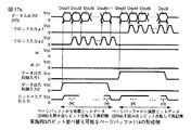
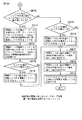
さらに、実施例1と実施例2の構成上の差異は、図11と図4を比較すれば明らかなように、k-bitの情報ビットと”01010101....0101”、すなわち”01”をkビット繰り返したものとの排他的論理和を取ったビット列中の”010”の3bit連続したシンボルの発生数を数えるシンボルカウンタ112を有していることである。さらに、k-bitの情報ビットと”10101010...1010”、すなわち”10”をkビット繰り返したものとの排他的論理和を取ったビット列中の”010”の3bit連続したシンボルの発生数を数えるシンボルカウンタ113を有していることである。これらにより、実施例1のSE4およびSE8の符号変換を行った4通りの場合に対して、予め各変換後の情報ビット中の”010”の数を数えておき、定量比較することにより、前述のように問題となる”010”の3bit連続したシンボルの出現確率をより減少させている。
Further, the difference in configuration between the first embodiment and the second embodiment is that k-bit information bits and “01010101... 0101”, that is, “01”, as is clear from comparison between FIG. And a
<第2符号変換回路104の誤り訂正符号のシーケンス>
図12に実施例2の104の具体的シーケンスを示す。
104では、まず、SE15において、情報ビットの中の”010”の3bit連続したシンボルの発生数を数える”010”シンボルカウンタ108と、情報ビットの中の”101”の3bit連続したシンボルの発生数を数える”101”シンボルカウンタ109、シンボルカウンタ112および113とをリセットし、符号化の状態を表すフラグ1及びフラグ2をリセットする。
<Error Correction Code Sequence of Second
FIG. 12 shows a
In 104, first, in SE15, “010”
ついで、SE16において、kビットの情報ビット中の”010”の連続ビットの個数をカウントし”010”シンボルカウンタ108に記憶する。
Next, in SE16, the number of consecutive bits “010” in k information bits is counted and stored in the “010”
また、kビットの情報ビット中の”101”の連続ビットの個数をカウントし”101”シンボルカウンタ109に記憶する。さらに、kビットの情報ビットと、”01010101....0101”、すなわち”01”をkビット繰り返したものとの排他的論理和を取ったビット列中の”010”の3bit連続したシンボル数をカウントし、シンボルカウンタ112に記憶する。また、kビットの情報ビットと、”10101010....1010”、すなわち”10”をkビット繰り返したものとの排他的論理和を取ったビット列中の”010”の3bit連続したシンボル数をカウントし、シンボルカウンタ113に記憶する。
Further, the number of consecutive bits “101” in k information bits is counted and stored in the “101”
<カウンタ112,113の構成例>
例えば、本例に係るカウンタ112およびカウンタ113の構成例は、図13のように示される。図示するように、カウンタ112およびカウンタ113は、情報ビットの初めから、シフトレジスタに入力し、”000”検出回路と"111”検出回路を組み合わせて、カウンタで数えることにより実現することができる。図13において212は2入力AND回路を、214は2入力OR回路を示している。図13の上記2つのカウンタ108,109に接続された回路は、図10で述べた回路と同じなので、ここでは省略する。情報ビットは情報ビット入力より一連の情報ビットを順に時系列にて入力するものとする。図13で、カウンタ112に接続された”000”出力と記した回路では、”000”が順に入力された単位時間において、”000”出力が”L”から”H”となり、他の場合には”L”となる。この”000”は、”010”の3bit連続の情報ビットと、”01010101....0101”ビットマスク中の”010”マスクで排他的論理和をとった場合に相当する。また、カウンタ112に接続された”111”出力と記した回路では、”111”が順に入力された単位時間において、”111”出力が”L”から”H”となり、他の場合には”L”となる。この”111”は、”010”の3bit連続の情報ビットと、”01010101....0101”ビットマスク中の”101”マスクで排他的論理和をとった場合に相当する。ここで、情報ビットを与えるクロックを1/2分周器213で分周すると、その出力は、例えば、情報ビットのxビット目として、xビットの偶数奇数にて”1”、”0”がそれぞれ出力される。よって、シンボルカウンタ112に電気的に接続された入力は、例えば、(”000”出力の論理が“H”で、かつ、xビット目が奇数の場合)と、(”111”出力の論理が”H”で、かつ、xビット目が偶数の場合)との論理和となり、これは、情報ビットと、”01010101....0101”との排他的論理和を取ったビット列中の”010”の3bit連続したシンボルが存在する場合に3連続シンボルの最後のシンボルが入力した単位時間で”H”、そのほかの場合に“L”となる。一方、シンボルカウンタ113に電気的に接続された入力は、例えば、(”111”出力の論理が“H”で、かつ、xビット目が奇数の場合)と、(”000”出力の論理が”H”で、かつ、xビット目が偶数の場合)との論理和となる。これは、情報ビットと、”10101010....1010”との排他的論理和を取ったビット列中の”010”の3bit連続したシンボルが存在する場合に3連続シンボルの最後のシンボルが入力した単位時間で”H”、そのほかの場合に“L”となる。よって、これら2入力OR回路214の出力を情報ビット入力の単位時間と同期させ、例えば、前記単位時間でOR出力の論理値が安定したところでトリガしてカウントすることにより、”01010101....0101”、すなわち”01”をkビット繰り返したビット列との排他的論理和を取ったビット列中の”010”の3bit連続したシンボル数をシンボルカウンタ112でカウントでき、また、kビットの情報ビットと、”10101010....1010”、すなわち”10”をkビット繰り返したビット列との排他的論理和を取ったビット列中の”010”の3bit連続したシンボル数をシンボルカウンタ113でカウントできる。例えば、図13のカウンタは一般に知られるバイナリカウンタで構成すればよいので、ここではカウンタの詳細は省略する。
<Configuration example of
For example, a configuration example of the
ついで、SE17において、108カウンタと109カウンタとの最小値が、112カウンタと113カウンタとの最小値より大きいか判断する。 Next, in SE17, it is determined whether the minimum values of the 108 counter and the 109 counter are larger than the minimum values of the 112 counter and the 113 counter.
ここで、SE17にてYesの場合、SE18にて、情報ビットと第一ビットマスクパターン”01010101....0101”(”01”をkビット分繰り返し発生させたもの)との排他的論理和をとるシーケンスを行い、情報ビットと置き換えを行い、フラグ1をセットする。
If YES in SE17, the exclusive OR of the information bits and the first bit mask pattern “01010101 .... 0101” (“01” repeated for k bits) in SE18 Is performed, the information bit is replaced, and the
ついで、SE19にて、シンボルカウンタ112の値と、シンボルカウンタ113の値より大きいか判断を行う。
Next, at SE19, it is determined whether the value of the
ここで、シンボルカウンタ112の値がシンボルカウンタ113の値より大きい場合には、SE20にて、kビットの情報ビットを全部ビット反転、すなわち”0”ビットを”1”ビット、”1”ビットを”0”ビットに変化させ、フラグ2をセットする。
Here, when the value of the
次いで、SE23にて情報ビットにフラグ1およびフラグ2に相当する符号を付加する。
Next, in SE23, codes corresponding to
一方、SE17のNoと判断した場合には、SE21にて、”010”シンボルカウンタ108の値と、”101”シンボルカウンタ109の値より大きいか判断を行う。
On the other hand, when it is determined No in SE17, it is determined in SE21 whether the value of the “010”
ここで、”010”シンボルカウンタ108の値が”101”シンボルカウンタ109の値より大きい場合には、SE22にて、kビットの情報ビットを全部ビット反転、すなわち”0”ビットを”1”ビット、”1”ビットを”0”ビットに変化させ、フラグ2をセットする。
Here, if the value of the “010”
次いで、SE23にて情報ビットにフラグ1およびフラグ2に相当する符号を付加する。
Next, in SE23, codes corresponding to
以上のシーケンスを経ることにより、実施例1のSE4およびSE8の符号変換を行った4通りの場合に対して、予め各変換後の情報ビット中の”010”の数を数えておき、定量比較することにより、前述のように問題となる”010”の3bit連続したシンボルの出現確率をより減少させている。尚、本実施例の第二符号の復号化は実施例1で述べた方法を用いればよいのでここでは省略する。 Through the above sequence, the number of “010” in the information bits after each conversion is counted in advance for the four cases where the code conversion of SE4 and SE8 of the first embodiment is performed, and quantitative comparison is performed. By doing so, the appearance probability of the consecutive symbols of “010”, which is a problem as described above, is further reduced. Note that the decoding of the second code in the present embodiment is omitted here because the method described in the first embodiment may be used.
ここで、比較例の図2中の(iii)および(iv)で示した、隣接メモリセルのしきい値電圧上昇による消去しきい値の増大する問題が生じるパターンは、当該メモリセル(α)が消去状態、BL方向に隣接するセル(β、γ)が書き込み状態となるので、ビット列としては”010”に相当する。ここで、図9(a1)から(a4)で示すように、104のシーケンスがない比較例の構成では、”01010101....0101”のkビットの系列では、”010”が[(k/2)-1]個含まれ、この箇所分、隣接メモリセルのしきい値電圧上昇による消去しきい値の増大する問題が大きな確率で生じる。例えば、1つのメモリセルαが図2の書き込みしきい値(v)との重なりが生じたり、読み出しレベルが書き込みしきい値とする判断するしきい値が超え、消去ビットが書き込みビットと誤認識され不良する確率p0とすると、p0が十分1より小さいとして、[(k/2)-1]×p0の不良が生じる。 Here, as shown in (iii) and (iv) of FIG. 2 of the comparative example, the pattern in which the problem that the erase threshold value increases due to the threshold voltage rise of the adjacent memory cell is the memory cell (α) Is in the erased state, and the cells (β, γ) adjacent in the BL direction are in the written state, so that the bit string corresponds to “010”. Here, as shown in FIGS. 9 (a1) to (a4), in the configuration of the comparative example without 104 sequences, in the k-bit series of “01010101 .... 0101”, “010” is [(k / 2) -1] is included, and the problem that the erase threshold value increases due to the threshold voltage increase of the adjacent memory cell occurs with a large probability. For example, one memory cell α is overlapped with the write threshold value (v) in FIG. 2 or the threshold for determining the read level as the write threshold is exceeded, and the erase bit is erroneously recognized as the write bit. Assuming that the failure probability is p0, it is assumed that p0 is sufficiently smaller than 1, and a failure of [(k / 2) -1] × p0 occurs.
ここで、実施例1よりも実施例2において、より”010”の3ビット列が生じる確率を小さく出来る例を図14(a)に示す。 Here, FIG. 14A shows an example in which the probability that a 3-bit string “010” is generated more in the second embodiment than in the first embodiment can be reduced.
図14(a)のように、実施例2の104に入力されるデータパターンでは、”010”の連続する3ビットシンボルが生じる個数はカウンタ108に記憶され(k/4)-1個、”101”の連続する3ビットシンボルが生じる個数はカウンタ109に記憶され(k/4)-1個、”01010101....0101”、すなわち”01”をkビット繰り返したものとの排他的論理和を取ったビット列中の”010”の3bit連続したシンボル数はカウンタ112に記憶され0個、”10101010....1010”、すなわち”10”をkビット繰り返したビット列との排他的論理和を取ったビット列中の”010”の3bit連続したシンボル数はカウンタ113に記憶され1個となる。よって、実施例1の104のシーケンスでは、104出力で"010”の生じるシンボルの個数は(k/4)-1個のままであるが、本実施例の104のシーケンスを用いることにより、104出力で”010”の生じるシンボルの個数を0個に減少させることができる。勿論、実施例1の(1)、及び(2)の効果は本実施例でも得ることができる。
As shown in FIG. 14 (a), in the data pattern input to 104 of the second embodiment, the number of occurrences of “010” consecutive 3-bit symbols is stored in the counter 108 (k / 4) −1, “ The number of occurrences of “101” consecutive 3-bit symbols is stored in the counter 109 (k / 4) −1, and the exclusive logic of “01010101... 0101”, ie “01” repeated k bits The number of consecutive 3 bits of “010” in the summed bit string is stored in the
また、勿論、本実施例の各カウンタの比較では、実施例1と同じマスクビットとビット反転パターンの4通りの場合について、SE3の比較よりも、より”010”の3連続シンボルの出現個数を正確に比較したものなので、例えば、図9(a)や図9(c)のように、比較例の”010”が最悪[(k/2)-1]個生じる場合でも、同じく{(k/4)を整数に切り上げた値}-1以下に抑制できることは明白である。例えば、1つのメモリセルαが図2の書き込みしきい値(v)との重なりが生じたり、読み出しレベルが書き込みしきい値とする判断するしきい値が超え、消去ビットが書き込みビットと誤認識され不良する確率p0とすると、p0が十分1より小さいとして、比較例の[(k/2)-1]×p0の不良が生じる確率を、[{(k/4)を整数に切り上げた値}-1]×p0まで低下させることができる。この実施例2の場合の”010”の3連続シンボルの出現個数が最も増加する最悪パターンの1例は、図9(e)のようなビット列となる。 Of course, in the comparison of each counter of this embodiment, the number of occurrences of three consecutive symbols “010” is more than that of the comparison of SE3 in the case of the same four mask bits and bit inversion patterns as in the first embodiment. For example, as shown in FIG. 9 (a) and FIG. 9 (c), even when “010” in the comparative example has the worst [(k / 2) −1] pieces as shown in FIG. It is obvious that the value of / 4) rounded up to an integer} -1 can be suppressed. For example, one memory cell α is overlapped with the write threshold value (v) in FIG. 2 or the threshold for determining the read level as the write threshold is exceeded, and the erase bit is erroneously recognized as the write bit. Assuming that the probability of failure is p0, assuming that p0 is sufficiently smaller than 1, the probability of occurrence of a failure of [(k / 2) -1] × p0 in the comparative example is obtained by rounding up [{(k / 4) to an integer. } -1] × p0. One example of the worst pattern in which the number of appearances of three consecutive symbols “010” in the second embodiment increases most is a bit string as shown in FIG.
[実施例3(ページバッファ114を更に備える一例)]
次に、実施例3に係るデータ記憶システムについて、図15乃至図19を用いて説明する。まず、本発明の実施例3の全体構成例を図15に示す。
[Example 3 (an example further including a page buffer 114)]
Next, a data storage system according to the third embodiment will be described with reference to FIGS. First, FIG. 15 shows an example of the overall configuration of the third embodiment of the present invention.
この実施例3によれば、上記実施例2の実施に加えて、さらに、”010”の3bitの連続シンボルの出現個数を減らすことができる。実施例1や実施例2と同一の部分や同一の動作部分には、同一符号をつけて詳しい説明は省略する。以下、説明や図では、情報ビットのkビット中を時系列で入出力をする場合を想定し、時系列の最初から数えて偶数番目のビットを偶数ビット、奇数番目のビットを奇数ビットと簡略表現する。 According to the third embodiment, in addition to the implementation of the second embodiment, the number of appearance of “010” 3-bit continuous symbols can be further reduced. The same parts as those in the first and second embodiments and the same operation parts are denoted by the same reference numerals, and detailed description thereof is omitted. In the following explanations and figures, it is assumed that the information bits are input / output in time series, and the even bits are counted from the beginning of the time series as even bits and the odd bits are simplified as odd bits. Express.
実施例2と実施例3の構成上の差異は、図11と図15を比較すれば明らかなように、情報ビットの偶数ビットと奇数ビットとの並べ替えを行うページバッファ114をさらに有していることである。本実施例では実施例2で第2符号化に加え、ページバッファ114を用いて、さらに、情報ビットを1番目、3番目、5番目、....、(k-1)番目の奇数番目のビットと2番目、4番目、6番目、....、k番目の偶数番目のビットとに分け、奇数番目の情報ビットを順に誤り訂正符号回路102に出力した後に、偶数番目の情報ビットを順に並べ替えて誤り訂正符号回路102に出力し、復号時には第二符号復号化回路105にて逆に並べ替えることにより、より”010”の3ビットの連続シンボルを減らすものである。なお、本実施例では、その特徴上、情報ビットの総数のkビットを偶数であるものと前提するが、通常のNAND入出力、図15の第一の内部I/O線でのデータ伝達は1バイト(=8ビット)x整数倍の単位のデータ入出力が行われるので実用上問題はなく、奇数ビット場合は実施例1内でのべた方法で拡張符号を形成すればよい。
The difference in configuration between the second embodiment and the third embodiment is that a
情報ビットの上述の並べ替えを行うページバッファ114は、例えば、隣接メモリセルのディスターブを低減する第二符号変換回路104に接続され、また、隣接メモリセルのディスターブを低減する第二符号逆変換回路105に接続される。また、このページバッファ114は少なくとも情報ビット数と同じk-bitのページバッファからなり、例えば、誤り訂正復号回路103で用いられるn-bitのシフトレジスタのフリップフロップを共通で用い、回路規模を縮小することができる。勿論、回路規模を縮小する必要がない場合は、誤り訂正復号回路103で用いられるn-bitのシフトレジスタと別に形成してもよい。
The
<ページバッファ114の具体的な回路例>
図16(a)、および図16(b)は本実施例のページバッファ114の具体的な回路例である。図をわかりやすくするために、図16(a)では、情報ビットを1番目、3番目、5番目、....、(k-1)番目の奇数番目のビットと2番目、4番目、6番目、....、k番目の偶数番目のビットとに分離して誤り訂正符号回路102に出力する回路部分は省略し、この部分は図16(b)にて示している。
<Specific circuit example of
FIG. 16A and FIG. 16B are specific circuit examples of the
なお、図16(a)のQ2,Q3となるトランジスタと配線を図16(b)の相当部分に適用することにより、全体の回路構成となるようにしている。なお、Q1からQ8としては、NMOSトランジスタを例としているが、勿論、入力を反転すればPMOSトランジスタでもよいし、後述の双方向性スイッチを用いても勿論よい。 Note that the transistors and wirings Q2 and Q3 in FIG. 16 (a) are applied to the corresponding parts in FIG. 16 (b), so that the entire circuit configuration is obtained. As Q1 to Q8, an NMOS transistor is taken as an example. Of course, a PMOS transistor may be used if the input is inverted, or a bidirectional switch described later may be used.
図16(a)では、誤り訂正復号回路103で用いられるn-bitのシフトレジスタの一部を想定し、k-bitのD型フリップフロップ208a,208bを、Q1を介して直列接続することにより情報ビット数と等しいk-bitシフトレジスタを形成している。ここで、208a,208bとしてはD型フリップフロップを用いたが、勿論ラッチ回路や、他のフリップフロップ回路で回路を形成してもよい。ここでは、D型フリップフロップとして、△印のクロック入力のパルス立ち上がり時に、クロック入力が"L"(ここでは便宜的に0[V]とする)から"H"(ここでは便宜的にVccとする)に立ち上がる瞬間に、Q出力がD入力に入ったデータで確定し、それ以後はクロックが"H"のままでも"L"のままでも"H"から"L"へ変化しても出力は変化しないエッジトリガー(edge trigger)型のフリップフロップとする。Q1のゲート電極は、Slと書いた入力に共通接続されている。Slを例えば0VからVccとし、遮断状態から導通状態にすることにより、iを1から(k-1)の整数として、直列接続された(i+1)ビット目の208aまたは208bの出力と、iビット目の208aまたは208b入力が接続されるようになっている。すなわち全体としてkビットのシフトレジスタとして動作するようになっている。なお、ここでは、シフトレジスタとしての動作を鑑み、先に入力してシフトするビットの添え字を小さい方に割り当てることとし、先のフリップフロップからFF1,FF2, ....FF(k/2)、FF(k/2+1)、....FF(k)と順に図16(a)及び図16(b)では記載する。なお、図16(b)ではFF1,FF2,....FF(k/2)までとFF(k/2+1)、....FF(k)とで折り返して表示しているが、図16(a)と同じフリップフロップの接続回路となっている。
In FIG. 16 (a), a part of the n-bit shift register used in the error
また、215のNMOS,216のPMOS、およびインバータ209によって、双方向性スイッチが形成されている。双方向性スイッチは、データ出力制御入力1または2が"H"の場合に、215と216の電流端子が導通状態となり、"L"の場合に遮断状態となる回路で、しきい値低下なくNMOS 215やPMOS 216の電流端子間で電圧を転送することができる特徴を有するが、例えば、しきい値による出力低下が問題ない場合には、NMOSトランジスタにて代用してもよい。ここで、Q5および双方向性スイッチ、およびビットマスク列入力との排他的論理和をとる素子217により、FF1の出力は、FF(k)の入力にフィードバックされる、いわゆる線形フィードバックシフトレジスタ(Linear Feedback Shift Resistor:LFSR)となっている。よって、このk段のシフトレジスタによって、情報ビットのkビットをFirst-In-First-Out(FIFO)で、かつ、情報をFF1,FF2、....、FF(k)に保持されている情報を順にクロック入力に応じて出力することができる。図17(a)にその回路の動作を示す。まず、kビットの1連のシフトレジスタとして動作させるために、読み出しおよび記憶時に、slをVcc("H")、/sl、p1およびビットマスク列入力を0V("L")にする。
Further, a bidirectional switch is formed by the
D型フリップフロップにデータを記憶する場合には、まず、データ出力制御入力1,2を共に"L"とし、フリップフロップ208の出力がデータ入出力線に出力されないようにする。さらに、データ入出力(I/O)線にVcc("H")か0V("L")の第一ビットのディジタルデータを与えた後、クロック入力1,2を共に"L"から"H"にする。これにより、第一ビットのディジタルデータが図16(a)の最も左側のフリップフロップFF(k)に保持される。ついで、データ入出力(I/O)線にVcc("H")か0V("L")の第二のディジタルデータを与えた後、クロック入力φ1,φ2を共に"L"から"H"にする。これにより、第一ビットのディジタルデータが図16(a)の左から2番めのフリップフロップFF(k-1)に転送および保持され、最も左側のフリップフロップFF(k)に第二のディジタルデータが保持される。後は、順次k[bit]までデータ入出力(I/O)線にディジタルデータを与え、クロックを与えることにより、図16(a)の右のフリップフロップから順にディジタルデータが保持され、k[Bit]のデータを保持することができる。
When data is stored in the D-type flip-flop, first, both the data
次に104からデータを読み出す際には、まず、データ出力制御入力1を"H"とし、データ出力制御入力2とビットマスク列入力を"L"とし、最も右側のフリップフロップFF1の出力をデータ入出力線に出力する。これによりデータ入出力線には第一ビットのディジタルデータのデータと同じデータが出力される。さらに、クロック入力φ1,φ2を共に"L"から"H"にする。これにより、左から右のフリップフロップに1ビットデータが転送および保持される。その結果、データ入出力線には第一ビットのディジタルデータのデータと同じデータが出力される。後は、全部で(k-1)回クロック入力φ1,φ2を共に"L"から"H"にすることにより、データ入出力(I/O)線に図16(a)の右のフリップフロップから順にデータが出力され、k[Bit]のデータを出力することができる。以上により、図16(a)の回路でk[bit]のデータをシーケンシャルに記憶し、記憶した順序で取り出せることは明らかである。
Next, when reading data from 104, first, the data
一方、図16(a)において、Q2およびQ3のゲート電極は、/Slと書いた入力に共通接続されている。Q3のゲート入力の/Slを例えば0VからVccとし、遮断状態から導通状態にすることにより、Q3と記されたトランジスタによって、前記kビットのシフトレジスタの奇数番目のビットのD型フリップフロップ208bが電気的に直列接続され、(k/2)個のシフトレジスタが形成できるようになっている。具体的には、Q3を介して、例えば、iを1から(k/2)-1までの整数として、(2i+1)番目のビットの208b出力が(2i-1)番目のビットの208b入力に接続されている。さらに、Q2のゲート入力の/Slを例えば0VからVccとし、遮断状態から導通状態にすることにより、Q2と記されたトランジスタを介して、前記kビットのシフトレジスタの偶数番目のビットのD型フリップフロップ208aが電気的に直列接続され、(k/2)個のシフトレジスタが形成できるようになっている。具体的には、例えば、iを1から(k/2)-1までの整数として、(2i+2)番目のビットの208a出力が(2i)番目のビットの208a入力に接続されている。
On the other hand, in FIG. 16 (a), the gate electrodes of Q2 and Q3 are commonly connected to the input written as / Sl. By changing / Sl of the gate input of Q3 from 0V to Vcc, for example, and switching from the cut-off state to the conductive state, the transistor indicated by Q3 causes the odd-numbered bit D-type flip-
ここで、双方向性スイッチ、およびビットマスク列入力との排他的論理和をとる素子217により、FF1の出力は、FF(k-1)の入力にフィードバックされる、いわゆる線形フィードバックシフトレジスタ(Linear Feedback Shift Resistor:LFSR)となっている。さらに、Q4により、/SlがVcc(”H”)の場合に、FF(k-1)の入力はデータ入出力(I/O)と接続されるようになっている。よって、この(k/2)段のシフトレジスタによって、情報ビットの奇数ビットである(k/2)ビットをFirst-In-First-Out(FIFO)で、かつ、情報をFF1,FF3、FF5,....、FF(k-1)に保持されている情報を順にクロック入力φ2に応じて出力することができる。
Here, the output of FF1 is fed back to the input of FF (k-1) by a bidirectional switch and an
また、Q6および双方向性スイッチ、および217のビットマスク列入力との排他的論理和をとる素子217により、FF2の出力は、FF(k)の入力にフィードバックされる、いわゆる線形フィードバックシフトレジスタ(Linear Feedback Shift Resistor:LFSR)となっている。よって、この(k/2)段のシフトレジスタによって、情報ビットの偶数ビットである(k/2)ビットをFirst-In-First-Out(FIFO)で、かつ、情報をFF2,FF4、FF6,....、FF(k)に保持されている情報を順にクロック入力φ1に応じて出力することができる。これらは偶数ビットと奇数ビットでビットが混合することなく独立に情報の読み出し及び記憶が可能である。
The output of FF2 is fed back to the input of FF (k) by the
図17(b)、17(c)にその回路の読み出しおよび記憶動作を示す。まず、(k/2)ビットの1連のシフトレジスタとして動作させるために、読み出しおよび記憶時には、/slをVcc("H")、sl、p1、およびビットマスク列入力を0V("L")とする。 FIGS. 17 (b) and 17 (c) show reading and storing operations of the circuit. First, in order to operate as a series of (k / 2) -bit shift registers, / sl is set to Vcc ("H"), sl, p1, and bit mask string input to 0 V ("L") during reading and storing. ).
ここで、図17(c)の書き込みから説明する。奇数ビットのデータをD型フリップフロップに記憶する場合には、まず、データ出力制御入力1,2を"L"とし、フリップフロップ208の出力がデータ入出力線に出力されないようにする。さらに、データ入出力(I/O)線にVcc("H")か0V("L")の第一ビットのディジタルデータを与えた後、クロック入力φ2を"L"から"H"にする。これにより、第一ビットのディジタルデータ(1ビット目に相当)が図16(a)の左側から2番目のフリップフロップFF(k-1)に保持される。ついで、データ入出力(I/O)線にVcc("H")か0V("L")の第二のディジタルデータ(1つ飛ばした3ビット目に相当)を与えた後、クロック入力φ2を"L"から"H"にする。これにより、第一ビットのディジタルデータが図16(a)の左から4番めのフリップフロップFF(k-3)に転送および保持され、左から2番目のフリップフロップFF(k-1)に第二のディジタルデータが保持される。後は、順次(k-1)[bit]までデータ入出力(I/O)線にディジタルデータを与え、クロックを与えることにより、図16(a)のフリップフロップで1つ飛ばしに順にディジタルデータが保持され、奇数ビットの全データ(k/2)ビット分のデータを保持することができる。
Here, the description starts from the writing in FIG. When storing odd-bit data in the D-type flip-flop, first, the data
また、偶数ビットのデータをD型フリップフロップにデータを記憶する場合には、まず、データ出力制御入力1,2を"L"とし、フリップフロップ208の出力がデータ入出力線に出力されないようにする。さらに、データ入出力(I/O)線にVcc("H")か0V("L")の第一ビットのディジタルデータを与えた後、クロック入力φ1を"L"から"H"にする。これにより、第一ビットのディジタルデータ(2ビット目に相当)が図16(a)の左側から1番目のフリップフロップFF(k)に保持される。ついで、データ入出力(I/O)線にVcc("H")か0V("L")の第二のディジタルデータ(1つ飛ばした4ビット目に相当)を与えた後、クロック入力φ1を"L"から"H"にする。これにより、第一ビットのディジタルデータが図16(a)の左から3番めのフリップフロップFF(k-2)に転送および保持され、最も左側のフリップフロップFF(k)に第二のディジタルデータが保持される。後は、順次k[bit]までデータ入出力(I/O)線にディジタルデータを与え、クロックを与えることにより、図16(a)のフリップフロップで1つ飛ばしに順にディジタルデータが保持され、偶数ビットの全データ(k/2)ビット分のデータを保持することができる。
Also, when storing even-bit data in the D-type flip-flop, first, the data
次に、図17(b)の読み出しを説明する。104から奇数ビットのデータを読み出す際には、まず、データ出力制御入力2を"H"とし、データ出力制御入力1を"L"とし、最も右側のフリップフロップFF1の出力をデータ入出力線に出力する。これによりデータ入出力線には、奇数ビットの第一ビットのディジタルデータと同じデータが出力される。さらに、クロック入力φ2を"L"から"H"にする。これにより、FF3の出力がFF1に転送および保持され、奇数ビットのデータが順に左から右のフリップフロップに転送および保持される。その結果、データ入出力線には奇数ビットの第二ビットのディジタルデータ(第3ビットに相当)と同じデータが出力される。後は、全部で(k/2-1)回クロック入力φ2を"L"から"H"にすることにより、データ入出力(I/O)線に図16(a)の右のフリップフロップで1つ飛ばしに順にデータが出力され、奇数ビットの全データ(k/2)ビット分のデータを1ビット目、3ビット目、5ビット目、....(k-1)ビット目と出力することができる。この際、クロック入力φ1は変化させないので、偶数ビットのデータは変化せず保持される。
Next, reading of FIG. 17B will be described. When reading odd-numbered bits from 104, first, set the data
一方、104から偶数ビットのデータを読み出す際には、まず、データ出力制御入力1を"H"とし、データ出力制御入力2を"L"とし、右側の2番目のフリップフロップFF2の出力をデータ入出力線に出力する。これによりデータ入出力線には、偶数ビットの第一ビットのディジタルデータと同じデータが出力される。さらに、クロック入力φ1を"L"から"H"にする。これにより、FF4の出力がFF2に転送および保持され、偶数ビットのデータが順に左から右のフリップフロップに転送および保持される。その結果、データ入出力線には偶数ビットの第二ビットのディジタルデータ(第4ビットに相当)のデータと同じデータが出力される。後は、全部で(k/2-1)回クロック入力φ1を"L"から"H"にすることにより、データ入出力(I/O)線に図16(a)の右のフリップフロップで1つ飛ばしに順にデータが出力され、偶数ビットの全データ(k/2)ビット分のデータを2ビット目、4ビット目、6ビット目、....(k)ビット目と出力することができる。この際、クロック入力φ2は変化させないので、奇数ビットのデータは変化せず保持される。
On the other hand, when reading even-numbered bit data from 104, first, the data
さらに、図17(d)左側に、フリップフロップ(208b)に保持されている奇数ビットデータ列と、例えば、”01010101....0101”のビットマスクとの排他的論理和を取り、排他的論理和を取ったデータを出力しつつフリップフロップ(208b)に再記憶する方法を示す。この場合は、ビットマスク列入力にビットマスクとなる”01010101....0101”入力パルスをクロック入力と同期して与える。 Further, on the left side of FIG. 17 (d), an exclusive logical sum of an odd-bit data string held in the flip-flop (208b) and, for example, a bit mask of “01010101. A method of re-storing data in the flip-flop (208b) while outputting data obtained by ORing will be described. In this case, a “01010101... 0101” input pulse serving as a bit mask is applied to the bit mask string input in synchronization with the clock input.
まず、データ出力制御入力2を"H"とし、データ出力制御入力1を"L"とし、最も右側のフリップフロップFF1の出力を排他的論理和素子217でビットマスク列入力の最初のビット”0”との排他的論理和でデータ入出力線に出力する。これによりデータ入出力線には、奇数ビットの第一ビットのディジタルデータと同じデータが出力される。さらに、クロック入力φ2を"L"から"H"にする。これにより、FF3の出力がFF1に転送および保持され、奇数ビットのデータが順に左から右のフリップフロップに転送および保持される。その結果、排他的論理和素子217でビットマスク列入力の2番目のビット”1”との排他的論理和をとりデータ入出力線に出力する。よって、この場合には、データ入出力線には奇数ビットの第二ビットのディジタルデータ(第3ビットに相当)の反転データが出力される。後は、全部で(k/2-1)回クロック入力φ2を"L"から"H"にすることにより、データ入出力(I/O)線に図16(a)の右のフリップフロップで1つ飛ばしに順にデータが出力され、奇数ビットの全データ(k/2)ビット分のデータを1ビット目、3ビット目、5ビット目、....(k-1)ビット目と、それぞれビットマスク列入力の1ビット目、2ビット目、3ビット目、....(k/2)ビット目との排他的論理和が順に出力される。また、最後に(k/2)回目のクロック入力φ2を"L"から"H"にすることにより、1ビット目、3ビット目、5ビット目、....(k-1)ビット目と、それぞれビットマスク列入力の1ビット目、2ビット目、3ビット目、....(k/2)ビット目との排他的論理和がFF1、FF3、FF5、....FF(k-1)のフリップフロップに再記憶される。この際、クロック入力φ1は変化させないので、偶数ビットのデータは変化せず保持される。なお、ここでは、ビット列マスク入力として”01010101....0101”を用いたが、勿論他のパターンでもよい。例えば、”11111111....1111”のビットマスクを用いることにより、図17(e)左側のように、フリップフロップ(208b)に保持されている奇数ビットデータ列をビット反転したデータを出力しつつフリップフロップ(208b)に再記憶する方法を容易に実現できる。
First, the data
さらに、図17(d)右側に、フリップフロップ(208a)に保持されている偶数ビットデータ列と、例えば、”01010101....0101”のビットマスクとの排他的論理和を取り、排他的論理和を取ったデータを出力しつつフリップフロップ(208a)に再記憶する方法を示す。この場合は、ビットマスク列入力にビットマスクとなる”01010101....0101”入力パルスをクロック入力と同期して与える。 Further, on the right side of FIG. 17 (d), an exclusive OR is taken between the even-bit data string held in the flip-flop (208a) and, for example, a bit mask of “01010101. A method of re-storing data in the flip-flop (208a) while outputting data obtained by ORing will be described. In this case, a “01010101... 0101” input pulse serving as a bit mask is applied to the bit mask string input in synchronization with the clock input.
まず、データ出力制御入力1を"H"とし、データ出力制御入力2を"L"とし、最も右側から2つ目のフリップフロップFF2の出力を排他的論理和素子217でビットマスク列入力の最初のビット”0”との排他的論理和でデータ入出力線に出力する。これによりデータ入出力線には、偶数ビットの第一ビットのディジタルデータと同じデータが出力される。さらに、クロック入力φ1を"L"から"H"にする。これにより、FF4の出力がFF2に転送および保持され、偶数ビットのデータが順に左から右のフリップフロップに転送および保持される。その結果、排他的論理和素子217でビットマスク列入力の2番目のビット”1”との排他的論理和をとりデータ入出力線に出力する。よって、この場合には、データ入出力線には偶数ビットの第二ビットのディジタルデータ(第4ビットに相当)の反転データが出力される。後は、全部で(k/2-1)回クロック入力φ1を"L"から"H"にすることにより、データ入出力(I/O)線に図16(a)の右のフリップフロップで1つ飛ばしに順にデータが出力され、偶数ビットの全データ(k/2)ビット分のデータを2ビット目、4ビット目、6ビット目、....(k)ビット目と、それぞれビットマスク列入力の1ビット目、2ビット目、3ビット目、....(k/2)ビット目との排他的論理和が順に出力される。また、最後に(k/2)回目のクロック入力φ1を"L"から"H"にすることにより、2ビット目、4ビット目、6ビット目、....(k)ビット目と、それぞれビットマスク列入力の1ビット目、2ビット目、3ビット目、....(k/2)ビット目との排他的論理和がFF2、FF4、FF6、....FF(k)のフリップフロップに再記憶される。この際、クロック入力φ2は変化させないので、奇数ビットのデータは変化せず保持される。なお、ここでは、ビット列マスク入力として”01010101....0101”を用いたが、勿論他のパターンでもよい。例えば、”11111111....1111”のビットマスクを用いることにより、図17(e)右側のように、フリップフロップ(208a)に保持されている偶数ビットデータ列をビット反転したデータを出力しつつフリップフロップ(208a)に再記憶する方法を容易に実現できる。勿論、このビットマスク列入力について、例えば、実施例1で説明したように、M系列などの平均化ビットマスク発生回路110の出力を入力することにすれば、図17で説明したシーケンスを用いて、符号出現確率平均化第一符号化回路106および、第一符号復号化回路107を実現することができる。
First, the data
さらに、図16(b)において、Q7のゲート電極は、p1と書いた入力に共通接続されている。Q7のゲート入力のp1を例えば0VからVccとし、遮断状態から導通状態にすることにより、Q7と記されたトランジスタによって、iを1からk/2の整数として、FF(k/2+i)の出力がFF(i)の入力に接続されている。また、iを1からk/2-1の整数として、FF(i+1)の出力がFF(k/2+i)の入力に接続されている。これにより、後で、図17(f)で示すように、隣接メモリセルディスターブ低減第二符号逆変換回路にて、符号化で偶数ビット列および奇数ビット列に分離された情報ビット列を、元の奇数-偶数-奇数-偶数....ビット列に逆変換して出力することができる。 Further, in FIG. 16 (b), the gate electrode of Q7 is commonly connected to the input written as p1. By changing the gate input p1 of Q7 from 0V to Vcc, for example, by switching from the cut-off state to the conductive state, Q is an integer from 1 to k / 2 by the transistor marked Q7, and FF (k / 2 + i) Is connected to the input of FF (i). The output of FF (i + 1) is connected to the input of FF (k / 2 + i), where i is an integer from 1 to k / 2-1. As a result, as shown in FIG. 17 (f), the information bit string separated into the even bit string and the odd bit string by the encoding in the adjacent memory cell disturb reduction second code inverse transform circuit is later converted into the original odd- Even-odd-even. . . . It can be converted back to a bit string and output.
図17(f)に、p1入力を”H”とすることにより、FF1、FF2、...、FF(k/2)に第二符号化前で奇数ビットだったデータが順に入力され、FF(k/2+1)、FF(k/2+2)、...FF(k)に第二符号化前で偶数ビットだったデータが順に入力されている場合に、FF1、FF(k/2+1)、FF2、FF(k/2+2)の順、すなわち、奇数偶数順でページバッファからデータを読み出すことができることを示す。 In FIG. 17 (f), by setting the p1 input to “H”, the data that was odd bits before the second encoding is sequentially input to FF1, FF2,. (k / 2 + 1), FF (k / 2 + 2), ... FF (k), when even-bit data before the second encoding is input in order, FF1, FF (k / 2 + 1), FF2, and FF (k / 2 + 2), that is, data can be read from the page buffer in the order of odd and even numbers.
ここでは、誤り訂正符号の復号化後の出力として、FF1、FF2、...、FF(k/2)に第二符号化前で奇数ビットだったデータが順に入力され、FF(k/2+1)、FF(k/2+2)、...FF(k)に第二符号化前で偶数ビットだったデータが順に隣接メモリセルディスターブ低減第二符号逆変換回路105に入力され、この符号列がページバッファ114に入力されている場合を想定している。まず、kビットの1連のシフトレジスタとして動作させるために、読み出しおよび記憶時に、p1をVcc("H")、sl、/sl、ビットマスク列入力を0V("L")とする。
Here, as the output after decoding of the error correction code, data that was odd bits before the second encoding is sequentially input to FF1, FF2, ..., FF (k / 2), and FF (k / 2 +1), FF (k / 2 + 2), ... FF (k) data that was even bits before the second encoding is sequentially input to the adjacent memory cell disturb reduction second code
104から第二符号化前の奇数-偶数-奇数-偶数....ビット列に逆変換して107に出力するには、以下のように行う。まず、データ出力制御入力1を"H"とし、データ出力制御入力2を"L"とし、右側の1番目のフリップフロップFF1の出力をデータ入出力線に出力する。これによりデータ入出力線には、奇数ビットの第一ビットのディジタルデータと同じデータが出力される。さらに、クロック入力φ1及びφ2を"L"から"H"にする。これにより、FF(k/2+1)の出力がFF1に転送および保持され、FF2の出力がFF(k/2+1)に転送および保持され、Q7の電流端子により電気的に接続された配線で、1ビット分フリップフロップに転送および保持される。その結果、データ入出力線には(k/2+1)番目のビットのディジタルデータと同じデータが出力される。さらに、クロック入力φ1及びφ2を"L"から"H"にする。これにより、データ入出力線には2番目のビットのディジタルデータと同じデータが出力される。
104 to odd-even-odd-even even before the second encoding. . . . Inverse conversion to a bit string and output to 107 is performed as follows. First, the data
後は、全部で(k-1)回クロック入力φ1を"L"から"H"にすることにより、データ入出力(I/O)線に読み出し前にFF1、FF(k/2+1)、FF2、FF(k/2+2)、....、FF(k/2)、FF(k)の順でデータが出力される。これは、第二符号化により奇数ビットデータと偶数ビットデータを分離して時系列で順に並べた場合に対して、逆変換を行い、元の符号の奇数-偶数-奇数-偶数....ビット列を復元して時系列で出力したことに他ならない。 After that, by changing the clock input φ1 from “L” to “H” a total of (k-1) times, FF1, FF (k / 2 + 1) before reading to the data input / output (I / O) line , FF2, FF (k / 2 + 2),. . . . , FF (k / 2) and FF (k) are output in this order. This is the case where the odd bit data and the even bit data are separated by the second encoding and arranged in time series, and the inverse transformation is performed, and the original code is odd-even-odd-even. . . . It is nothing but restoring the bit string and outputting it in time series.
以上より、本実施例のページカウンタ114を用いれば、従来のシフトレジスタを用いた誤り符号復号回路に対して、高々(情報ビット−1)x3+8トランジスタと2つのインバータ、及び2つの2入力排他的論理和素子だけで、実施例3に必要な第二符号化のための情報ビットの符号変換回路が実現できることが明らかである。
As described above, when the
<第二符号化回路104のシーケンス>
次に、図18を用いて、実施例3に係る第2符号化回路104の具体的シーケンスを示す。
<Sequence of
Next, a specific sequence of the
104では、まず、SE24において、フラグ1、フラグ2、および、フラグ3をリセットして、ページバッファ114より1ビット目、3ビット目、5ビット目、....(k-1)ビット目の奇数ビットの(k/2)ビット個数の情報ビットデータを読み出す。これには、奇数ビットをカウンタに出力する方法は、例えば、図17(b)左側の方法で奇数の情報ビットを出力し、図13の回路に入力すればよい。
In 104, first, in SE24,
ついで、SE25において、ページバッファ114より2ビット目、4ビット目、6ビット目、....kビット目の偶数ビットの(k/2)ビット個数の情報ビットデータを読み出す。例えば、図17(b)右側の方法で奇数ビット出力後に偶数の情報ビットを出力し、図13の回路に入力すればよい。
Next, in SE25, (k / 2) bits of information bit data of the second bit, the fourth bit, the sixth bit,... K bits are read from the
次いで、SE26にて、例えば、情報ビット内の”010”シンボルをカウンタ108にてカウントし、”101”シンボルをカウンタ109にてカウントし、kビット長さの上記奇数ビットと偶数ビットの連続したものを”01010101....0101”、つまり”01”をビット始めから繰り返し並べたものと排他的論理和を取った”010”シンボルをカウンタ112にてカウントする。さらに、kビット長さの情報ビットを”10101010....1010”、つまり”10”をビット始めから繰り返し並べたものと排他的論理和を取った”010”シンボルをカウンタ113にてカウントする。
Next, at SE26, for example, the "010" symbol in the information bits is counted by the
これには、SE24,SE25の情報ビットを図13の情報ビット入力に入力すればよい。 For this purpose, the information bits of SE24 and SE25 may be input to the information bit input of FIG.
ついで、SE27にて、シンボルカウンタ108,シンボルカウンタ109、シンボルカウンタ112,シンボルカウンタ113の値をレジスタa,b,c,dにそれぞれコピーする。
Next, at SE27, the values of the
ついで、SE28にて、実施例3のページバッファ114にて、ページバッファより1ビット目、2ビット目、3ビット目、....kビット目と奇遇奇遇順に、すなわち、通常の順番でkビットの情報ビットデータを読み出す。これには、図17(a)右側の方法で、情報ビットを出力すればよい。
Next, in SE28, in the
次いで、SE28にて、例えば、kビット長さの1ビット目、2ビット目、3ビット目、....kビット目と並んだ情報ビット内の”010”シンボルをカウンタ108にてカウントし、”101”シンボルをカウンタ109にてカウントし、”01010101....0101”、つまり”01”をビット始めから繰り返し並べたものと排他的論理和を取った”010”シンボルをカウンタ112にてカウントする。さらに、kビット長さの情報ビットを”10101010....1010”、つまり”10”をビット始めから繰り返し並べたものと排他的論理和を取った”010”シンボルをカウンタ113にてカウントする。これには、SE28の情報ビット出力を図13の情報ビット入力に入力すればよい。
Next, at SE28, for example, the
さらに、SE30にて、カウンタ108,109,112,113と、レジスタa,b,c,dのそれぞれ内容を比較して最小値となる内容を含むのはカウンタかレジスタかを求める。
Further, in SE30, the contents of the
この結果、次いでSE31にて、最小値になるのは、レジスタa,b,c,d はなく、カウンタ108,109,112,113の方であるか判断する。 As a result, in SE31, it is determined whether there is no register a, b, c, d, but counters 108, 109, 112, 113 which are the minimum values.
ここで、カウンタ108,109,112,113の方に最小値となる条件がある場合、フラグ3をリセットしたまま、SE17-SE22までと同じシーケンスを行う。
Here, when there is a condition that the
その後、SE23の替わりに、SE33にて、情報ビット(k-bit)にフラグ1、フラグ2、およびフラグ3に対応する符号を付加して102の誤り訂正符号発生回路に出力する。
Thereafter, in place of SE23, in SE33, codes corresponding to
ついで、カウンタ108,109,112,113の方に最小値となる条件がない場合、SE32でフラグ3をセットする。
Next, when there is no condition for the
ついで、情報ビットを奇数ビットと偶数ビットに分離して、例えば、1ビット目、3ビット目、5ビット目、....(k-1)ビット目、2ビット目、4ビット目、6ビット目、....kビット目と並べたものに対して情報ビットとし、SE17-SE22までと同様なシーケンスを行うものである。 Next, the information bits are separated into odd bits and even bits, for example, the first bit, the third bit, the fifth bit,. . . . (k-1) bit, 2nd bit, 4th bit, 6th bit,. . . . The information arranged for the kth bit is used as an information bit, and the same sequence as in SE17 to SE22 is performed.
ここで、SE34において、レジスタaおよびレジスタbの最小値が、レジスタcまたはレジスタdの最小値より大きいか判断する。 Here, in SE34, it is determined whether the minimum value of the register a and the register b is larger than the minimum value of the register c or the register d.
ここで、SE34にてYesの場合、SE35にて、フラグ1をセットし、情報ビットの奇数ビットと、第一ビットマスクパターン”01010101....0101”(”01”をビット初めから(k/2)ビット分繰り返し発生させたもの)との排他的論理和をとるシーケンスを行い、ページバッファ114に再記憶する。これには、図17(d)左側のシーケンスを行えばよい。
Here, if Yes in SE34,
ついで、SE36において、情報ビットの偶数ビットと、第一ビットマスクパターン”01010101....0101”(”01”をビット初めから(k/2)分繰り返し発生させたもの)との排他的論理和をとるシーケンスを行い、ページバッファ114に再記憶する。これには、図17(d)右側のシーケンスを行えばよい。
Then, in SE36, the exclusive logic of the even number of information bits and the first bit mask pattern “01010101 .... 0101” (“01” is repeatedly generated from the beginning of the bit by (k / 2)) A sequence for calculating the sum is performed and stored in the
ついで、SE37にて、シンボルカウンタ112の値が記憶されたレジスタcと、シンボルカウンタ113の値が記憶されたレジスタdより大きいか判断を行う。ここで、SE37にてYesの場合には、SE38にて、kビットの情報ビットを全部ビット反転、すなわち”0”ビットを”1”ビット、”1”ビットを”0”ビットに変化させ、フラグ2をセットする。これには、例えば、図17(e)のシーケンスを行えばよい。
Next, in SE37, it is determined whether the value of the register c storing the value of the
一方、SE34のNoと判断した場合には、SE39にて、”010”シンボルカウンタ108が記憶されたレジスタaの値と、”101”シンボルカウンタ109が記憶されたレジスタbの値より大きいか判断を行う。SE39にてYesの場合には、SE40にて、kビットの情報ビットを全部ビット反転、すなわち”0”ビットを”1”ビット、”1”ビットを”0”ビットに変化させ、フラグ2をセットする。これには、例えば、図17(e)のシーケンスを行えばよい。
On the other hand, if it is determined No in SE34, it is determined in SE39 whether the value of the register a storing the “010”
この後、SE41で、情報ビット中の208bのフリップフロップに入った奇数データを1ビット目、3ビット目、....、(k-1)ビット目を読み出し、誤り訂正符号化回路102に出力する。この情報の出力には、例えば、図17(b)左側のシーケンスで行えばよい。
After that, in SE41, the odd data entered in the flip-
さらに、SE42で、情報ビット中の208aのフリップフロップに入った偶数データを2ビット目、4ビット目、....、kビット目を読み出し、誤り訂正符号発生回路102に出力する。この情報の出力には、例えば、図17(b)右側のシーケンスで行えばよい。
Further, in SE42, the even data that has entered the 208a flip-flop in the information bits is converted into the second bit, the fourth bit,. . . . The k-th bit is read out and output to the error correction
さらに、SE43にて情報ビットにフラグ1、フラグ2、およびフラグ3に相当する符号を102に出力する。
Further, in SE43, codes corresponding to the
なお、実施例1と同様に、フラグ1、フラグ2、およびフラグ3を情報ビットに付加する方法として、各フラグを2ビットの連続するデータとして情報ビットに付加する方法がある。この方法は、フラグ1,2がどの状態でも”010”の状態が生じないように選択しているが、勿論、これ以外の符号化、例えば、フラグ1、2,3のいずれか2つを同一2ビット割り当て、残り1つのフラグを1ビットに割り当てる方法でも良い。これは、情報ビットの前または後ろにフラグ1,2,3に対応するビットがaabbcc(a,b,cはそれぞれフラグ1,2,3に相当する”0”,”1”の状態)となっているが、ccbbaa、aabbcやccbbaなど適宜順番を入れ替えたものをフラグに対応するビットとして付加してもよい。勿論、このフラグに相当するビットは、情報ビットの前後に付加するのではなく、例えば、情報ビットを2つに分け、ccbbaaのようにして情報ビットの中に埋め込んでもよい。勿論情報ビットを4つに分け、aa,bb,ccをそれぞれ4つの情報ビットの間に入るように埋め込んでもよい。また、誤り訂正符号化した後に、検査ビット(パリティ)ビットを数個に分割し、aa、bb、ccのように2個以上の同じビットからなるフラグを検査ビットで挟むように並べ替え(インタリーブ)してもよい。このようにすれば、2個以上の同じビットからなるフラグの両側のビットは”010”パターンになり得ないため、より、検査ビット部分の”010”パターンの生じる可能性を減少できる。
As in the first embodiment, as a method of adding the
<第二符号逆変換回路105の復号化のシーケンス>
次に、図19を用いて、本実施例3の第二符号逆変換回路105の復号化の具体的シーケンスを説明する。
<Decoding Sequence of Second Code
Next, a specific sequence of decoding by the second code
第二符号逆変換回路105では、まず、SE44において、情報ビットに付加されたフラグ1、フラグ2およびフラグ3に相当する情報を、例えば、レジスタや一時メモリに記憶する。
In the second code
ついで、SE45にて、フラグ2がセットされているか判断後、フラグ2がセットされている場合には、SE46にて、kビットの情報ビットを全部ビット反転、すなわち”0”ビットを”1”ビット、”1”ビットを”0”ビットに変化させ、情報ビットと置き換える。
Then, after determining whether
ついで、SE45のNoと判断した分岐と合流後、SE47にて、フラグ1がセットされているか判断する。
Next, after joining the branch determined to be No in SE45, it is determined in SE47 whether the
SE47でYes、すなわちフラグ1がセットされている場合、SE48で情報ビットと第一ビットマスクパターン”01010101....0101”(”01”をkビット分繰り返し発生させたもの)との排他的論理和をとるシーケンスを行い、情報ビットと置き換えを行う。この第一ビットマスクパターンは、104の符号化の際”10”をkビット分繰り返し発生させた、”10101010....1010”を用いた場合には、同じ”10101010....1010”マスクビットを用いれば良い。
When SE47 is Yes, that is, when
ついで、SE47のNoと判断した分岐と合流後、SE49にて、フラグ3がセットされているか判断する。
Next, after joining the branch determined to be No in SE47, it is determined in SE49 whether the
さらに、フラグ3がセットされている場合、SE50にて、FF1、FF2、...、FF(k/2)に第二符号化前の奇数データが順に入力され、FF(k/2+1)、FF(k/2+2)、...FF(k)に第二符号化前の偶数データが順に入力されているので、FF1、FF(k/2+1)、FF2,FF(k/2+2)の順、すなわち、第二符号化前の奇数偶数順でページバッファからデータを読み出し、第一符号復号化回路107に出力する。これには、例えば、図17(f)のシーケンスを用いればよい。
Further, when
フラグ3がセットされていない場合には、ページバッファ114より1ビット目、2ビット目、3ビット目、....kビット目と奇遇奇遇順に、すなわち、通常の順番でkビットの情報ビットデータを読み出し、第一符号復号化回路107に出力すればよい。
If
以上のシーケンスを経ることにより、実施例3の符号変換を行った8通りの場合に対して、予め各変換後の情報ビット中の”010”の数を数えておき、定量比較することにより、前述のように問題となる”010”の3bit連続したシンボルの出現確率をより減少させている。 By performing the above sequence, the number of “010” in the information bits after each conversion is counted in advance for the eight cases where the code conversion of the third embodiment is performed, and by quantitative comparison, As described above, the appearance probability of the consecutive 3 bits of “010” which is a problem is further reduced.
ここで、実施例1,2よりも実施例3において、より”010”の3ビットシンボルの列が生じる確率を小さく出来ることを、図20(a)を例に挙げて示す。図20(a)では、実施例2の場合の”010”の3連続シンボルの出現個数が最も増加する最悪パターンの1例である図9(e)のようなビット列を入力した場合を示す。この場合、奇数ビットと偶数ビットを1ビット目、3ビット目、5ビット目、....(k-1)ビット目、2ビット目、4ビット目、6ビット目、....kビット目と並べかえを行うことにより、図20(a1)の(k/2)ビットの”10101010....1010”と(k/2)ビットの”00000000.... 0000”の情報ビットが、図20(a2)の(k/4)ビットの” 11111111....1111”と、(3k/4)ビットの”00000000.... 0000”の情報ビットに並べ替えがされるので、”010”が生じる個数を0まで削減できる。これにより、図20(a)に対応するデータは並べ替えされ、フラグ1、2,3がそれぞれリセット、リセット、セットとなる。この結果、誤り訂正符号発生回路102に出力される符号列例を図20(a3)に示す。このようにすることにより、フラグを含めた情報ビットで”010”の生じる個数を0まで削減できる。なお、今回は説明を簡単にするため、全ビット反転や情報ビットとの”01010101....0101”との排他的論理和を取っていない場合を示したが、図20(a)の符号に今回は全ビット反転や情報ビットとの”01010101....0101”との排他的論理和を取ったり、その両方を行った場合も、実施例3のシーケンスで同様に”010”の生じる個数を0個にできる。これは、例えば、”10101010....1010 00000000.... 0000”ではなく、”10101010....1010 11111111.... 1111”の情報ビットの場合に当てはまる。
Here, FIG. 20 (a) is used as an example to illustrate that the probability that a string of 3-bit symbols of “010” is more likely to be generated in the third embodiment than in the first and second embodiments. FIG. 20 (a) shows a case where a bit string as shown in FIG. 9 (e), which is an example of the worst pattern in which the number of occurrences of three consecutive symbols “010” increases most in the case of the second embodiment, is input. In this case, odd bits and even bits are the 1st, 3rd, 5th,. . . . (k-1) bit, 2nd bit, 4th bit, 6th bit,. . . . By rearranging with the k-th bit, the information bits of (k / 2) bits “10101010 .... 1010” and (k / 2) bits “00000000 .... 0000” in FIG. 20 (a1) However, since the (k / 4) bit “11111111 .... 1111” and (3k / 4) bit “00000000 .... 0000” information bits are rearranged in FIG. 20 (a2) , “010” can be reduced to zero. Thereby, the data corresponding to FIG. 20 (a) is rearranged, and the
よって、一般の16ビットより多いkビットの情報ビットでは、本実施例を用いることにより、最悪の”010”の生じる数は高々{(k/6)を整数に切り上げた値}-1以下の箇所に減少することができる。なぜなら、実施例1,2の議論と同様に考えて、仮に実施例3の符号変換を施した情報ビットの中に”010”の数は{(k/6)を整数に切り上げた値}-1よりも多いと仮定する。この場合、最悪、”010”が最も稠密に並んだ場合においても、”01010101....010”が(k/3)+1ビット以上連続したビットで占めることになる。よって、”010”以外のパターンのビット数は高々(2k/3)-1ビット以下である。ここで、”01010101....010”との排他的論理和により”010”パターンが増加し、その増加数が部分符号長あたり最も大きいパターンは”00000000....0000”である。よって、情報ビットとの”01010101....010”との排他的論理和を取った場合で、最悪の”010”の生じる箇所を高々{(k/6)を整数に切り上げた値}-1の箇所と限定するための最小の部分符号パターンは、”00000000....0000”が[(k/3)-1]ビット長さあり、”01010101....010”が(k/3)+1ビット以上連続したビット(連続ビットaパターンと以後呼ぶ)となる。よって、前述の仮定を満たすには、aパターン内の端の1ビットの”0”の重なりを考えて、kビットの全情報ビットにおいて、連続ビットaパターンを除いた残りの(k/3)+1ビット以下のビット数で実施例3の第二符号化で”010”の数が{(k/6)を整数に切り上げた値}-1よりも大きい情報ビットの組み合わせが存在する必要がある。ここで、実施例2および実施例3の図20(a)の符号化の議論より、実施例3の奇数ビットと偶数ビットを1ビット目、3ビット目、5ビット目、....(k-1)ビット目、2ビット目、4ビット目、6ビット目、....kビット目と並べかえるシーケンスは、実施例1,2の符号のビット反転を取るシーケンス、および、”01010101....0101”のビットマスクと情報ビットとの排他的論理和を取るシーケンスと、それぞれ独立に実施することができ、フラグ1,2,3で示す全部で8通りの状態を分けていることは明らかである。さらに、図20(a)では、前記偶数奇数ビット並べ替えのみで、連続ビットaパターンは、”010”の出現する数を0まで減少させることができる。よって、前述の仮定を満たすためには、連続ビットaパターンを除いた残り(k/3)+1ビット以下のビット数で、特に、前記偶数奇数ビット並べ替えで、{(k/6)を整数に切り上げた値}-1よりも”010”の連続パターンが増えるパターンである必要がある。偶数奇数ビット並べ替えで、”010”パターンが増えるパターンは”0x1x0x”(xは”0”または”1”のいずれか)のパターンがあり、特に、偶数奇数ビット並べ替えで、最も”010”パターンが偶数奇数ビット並べ替えで増えるパターンは”00110011....001100”の繰り返しパターンとなる。他のバリエーションとしては、”00110011....001100”の繰り返しパターンをビット反転したものや、前記繰り返しパターンに”01010101....0101”との排他的論理和を取ったもの、および両方を適用したものを含むパターンとなる。図20(b1)の右端のビット列がそれに相当しており、図20(b2)、(b3)、(b4)の符号の後ろ側(k/3)ビットが、実施例3の第二符号処理を施した場合のパターン変化を示している。この場合、図20(b3)では、最小で(k/6)-2個の”010”しか生じない。特に、実施例2で示したビット反転と”01010101....0101”との排他的論理和との組み合わせでは、”00110011....0011”部分では”010”の3連続ビットを生じないことに注意されたい。
Therefore, in the case of k information bits larger than general 16 bits, by using this embodiment, the number of occurrences of the worst “010” is at most {value obtained by rounding up (k / 6) to an integer} −1 or less. Can be reduced to locations. This is because the number of “010” in the information bits subjected to the code conversion of the third embodiment is {value obtained by rounding up (k / 6) to an integer} − Assume more than one. In this case, even when “010” is arranged most densely, “01010101... 010” is occupied by continuous bits of (k / 3) +1 bits or more. Therefore, the number of bits of the pattern other than “010” is at most (2k / 3) −1 bits. Here, the “010” pattern is increased by exclusive OR with “01010101 .... 010”, and the largest number of the increment per partial code length is “00000000 .... 0000”. Therefore, when the exclusive OR of “01010101 .... 010” with the information bit is taken, the place where the worst “010” occurs is at most {value obtained by rounding up (k / 6) to an integer} − The minimum partial code pattern for limiting to 1 is “00000000 .... 0000” is [(k / 3) -1] bits long, and “01010101 .... 010” is (k / 3) It is a continuous bit of +1 bit or more (hereinafter referred to as a continuous bit a pattern). Therefore, in order to satisfy the above-mentioned assumption, considering the overlap of 1 bit “0” at the end of the a pattern, the remaining information (k / 3) excluding the continuous bit pattern a in all k information bits There must be a combination of information bits in which the number of “010” in the second encoding of
ここで、一般には、並べ替えによって、{(k/6)を整数に切り上げた値}-1より”010”パターンが増えるには、最小でも(k/3)+4ビット以上の”00110011....001100”が必要となる。連続ビットaパターンの端の”00”の2ビットの重複を除くと、連続ビットaパターンを除いた残りは最低(k/3)+2ビット以上必要となる。よって、実施例3の符号変換を施した情報ビットの中に”010”の数は{(k/6)を整数に切り上げた値}-1よりも多いと仮定は矛盾するので、実施例3の符号変換を施した情報ビットの中に”010”の数は{(k/6)を整数に切り上げた値}-1以下になる。 Here, in general, in order to increase the “010” pattern from {value obtained by rounding up (k / 6) to an integer} -1 by reordering, “00110011.” is at least (k / 3) +4 bits or more. ... 001100 ”is required. Excluding the duplication of 2 bits of “00” at the end of the continuous bit a pattern, the remainder excluding the continuous bit a pattern requires at least (k / 3) +2 bits. Therefore, since the assumption contradicts that the number of “010” in the information bits subjected to code conversion in the third embodiment is larger than {value obtained by rounding up (k / 6) to an integer} −1, the third embodiment is contradictory. The number of “010” in the information bits subjected to the code conversion is {value obtained by rounding up (k / 6) to an integer} −1.
さらに、”00110011....0011”に第二の実施例のビット反転したものや、前記繰り返しパターンに”01010101....0101”との排他的論理和を取ったもの、および両方を適用したものも、”0011”の巡回パターン、例えば”01100110....0110”となるので、同様に高々(k/6)個-1以下の”010”しか生じない。 Furthermore, the bit-inverted version of the second embodiment is applied to “00110011 .... 0011”, the exclusive pattern of “01010101 .... 0101” is added to the repetitive pattern, and both are applied. Since the cyclic pattern of “0011”, for example, “01100110.... 0110” is also produced, only “010” of at most (k / 6) −1 or less is generated.
以上より、図20(b1)が実施例3での符号変換を行った場合でも”010”の個数が多い1例である。この場合、”010”の個数は(k/6)-2個に抑えられ、最悪の”010”の生じる数は高々{(k/6)を整数に切り上げた値}-1以下の箇所に減少することができる。図20(b1)の符号に、実施例2の全ビット反転や情報ビットとの”0101010....1010”との排他的論理和を取ったり、その両方を行った場合も、同様に、第3の実施例の符号化により、”010”の生じる個数を高々{(k/6)を整数に切り上げた値}-1以下の”010”にすることができる。 From the above, FIG. 20 (b1) is an example in which the number of “010” is large even when the code conversion in the third embodiment is performed. In this case, the number of “010” is limited to (k / 6) -2, and the worst occurrence of “010” is at most {value obtained by rounding up (k / 6) to an integer} -1 or less. Can be reduced. In the case where the sign of FIG. 20 (b1) is exclusive ORed with “0101010 .... 1010” of all bits inversion and information bits in the second embodiment, or both, By the encoding of the third embodiment, the number of occurrences of “010” can be reduced to “010” which is {value obtained by rounding up (k / 6) to an integer} −1.
なお、図20(c1)に、”010”のパターンを含み、かつ、全ビット反転や情報ビットとの”0101010....1010”との排他的論理和を取ったり、その両方を行った場合も、”010”のパターンほぼ等しく生じる”010”の発生頻度が高い例を示す。それぞれのレジスタa,b,c,dおよび、カウンタ108,109,112,113の値も右に示してある。このパターンは、”0100”もしくは、”0001”の4ビットの繰り返しとなっており、偶数奇数ビット並べ替えでも”010”の発生個数を減らすことができないパターンとなっている。”010”の個数は符号の時系列反転で不変量だから、時系列反転を考えた”0010”もしくは”1000”の繰り返しも同様のカウント数となることは明らかである。このパターンも、実施例3のシーケンスを行うことにより、上記同様に”010”の生じる個数を高々{(k/6)を整数に切り上げた値}-1以下、ここでは、(k/8)個以下の”010”にすることができ、前記図20(b)の方が”010”パターン個数が増えるパターンとなる。このように、”01010101....0101”、または、”10101010....1010”の連続ビットでは”010”の発生頻度は(ビット長/2)-1程度生じるが、”010”のシンボルに続いて他のビットを挿入して符号を作成した場合、例えば、”01000100....0100”の連続ビットでは、”010”は最大(ビット長さ/4)程度に減少する。よって、”010”の部分情報ビットあたりの発生ビット数は、図20(c)のパターンのように”010”を分散させて配置した場合は、”01010101....0101”、または、”10101010....1010”の連続ビットが実施例3の符号化により生じる場合に比較して、連続ビットの長さが16ビットより長い場合には1/2以下になる。 In FIG. 20 (c1), the pattern “010” is included, and all bits are inverted or exclusive OR of “0101010 .... 1010” with information bits is performed. In this case as well, an example is shown in which the frequency of occurrence of “010”, which is almost equal to the “010” pattern, is high. The values of the respective registers a, b, c, d and counters 108, 109, 112, 113 are also shown on the right. This pattern is a 4-bit repetition of “0100” or “0001”, and the number of occurrences of “010” cannot be reduced even by rearranging even and odd bits. Since the number of “010” is an invariable amount due to the time series inversion of the code, it is clear that the repetition of “0010” or “1000” considering the time series inversion also has the same count number. In this pattern as well, by performing the sequence of the third embodiment, the number of occurrences of “010” is at most {value obtained by rounding up (k / 6) to an integer} −1, where (k / 8) The number can be less than “010”, and the pattern shown in FIG. 20 (b) increases the number of “010” patterns. In this way, with the consecutive bits of “01010101 .... 0101” or “10101010... 1010”, the frequency of occurrence of “010” is about (bit length / 2) −1, but “010” When a code is created by inserting other bits following a symbol, for example, in a continuous bit of “01000100... 0100”, “010” is reduced to the maximum (bit length / 4). Therefore, the number of generated bits per partial information bit of “010” is “01010101 .... 0101” or “0” when “010” is distributed as shown in the pattern of FIG. Compared to the case where the continuous bits of 10101010... 1010 "are generated by the encoding of the third embodiment, when the length of the continuous bits is longer than 16 bits, it becomes 1/2 or less.
一方、実施例1,2の”010”の生じる個数の上限値、すなわち、{(k/4)を整数に切り上げた値}-1値と、実施例3のの”010”の生じる個数の上限値、すなわち、{(k/6)を整数に切り上げた値}-1との比はkが16ビット以上で、2倍以下である。また、kが20ビット以上では、2倍より小さくなる。よって、010”を分散させて配置した場合は”10101010....1010”の連続配置した場合に比べて、kが16ビット以上では、最悪の”010”の生じる個数の上限値以下となり、kが20ビット以上では、より小さくなる。 On the other hand, the upper limit of the number of occurrences of “010” in Examples 1 and 2, that is, {value obtained by rounding up (k / 4) to an integer} −1 value, and the number of occurrences of “010” in Example 3 The ratio to the upper limit value, that is, {value obtained by rounding up (k / 6) to an integer} -1 is k is 16 bits or more and 2 times or less. Also, when k is 20 bits or more, it is smaller than twice. Therefore, when 010 ”is distributed,“ 10101010. . . . When k is 16 bits or more, it is less than the upper limit of the number of occurrences of the worst “010”, and when k is 20 bits or more, it is smaller than when 1010 ”is continuously arranged.
上記のように、本実施例3によれば、少なくとも上記(1)乃至(2)と同様の効果が得られる。 As described above, according to the third embodiment, at least the same effects as the above (1) to (2) can be obtained.
さらに、以上から、本実施例3にて第二符号変換することにより、”010”パターンの生じる個数を、最悪、{(k/6)を整数に切り上げた値}-1以下に抑えることができる。よって、実施例3の操作を行うことによって、実施例1や2よりも最悪の”010”の生じる数は高々{(k/6)を整数に切り上げた値}-1の箇所まで減少させることができる。 Furthermore, from the above, by performing the second code conversion in the third embodiment, the number of occurrences of “010” patterns can be suppressed to the worst, {value obtained by rounding up (k / 6) to an integer} −1 or less. it can. Therefore, by performing the operation of the third embodiment, the number of occurrences of the worst “010” as compared with the first and second embodiments is reduced to {at the value obtained by rounding up (k / 6) to an integer} −1. Can do.
例えば、図29中の矢印Y3に示すように、”010”のシンボル数が100個程度の場合に、実施例1、2と比べ、”010”の出現する最悪状態数をさらに低減することができる。 For example, as shown by an arrow Y3 in FIG. 29, when the number of “010” symbols is about 100, the number of worst states in which “010” appears can be further reduced as compared with the first and second embodiments. it can.
なお、図20(b4)および図20(c4)をみれば明らかなように、実施例3の偶数奇数ビットの並べ替え後のパターンは”01010101....0101”、 ”10101010....1010”、” 0000000....0000”,”11111111....1111”の部分情報ビット列の組み合わせとなっている。よって、偶数奇数ビットの並べ替えを行った情報ビット列に対して、さらに偶数奇数ビットの並べ替えを行い、その後に、全ビット反転や情報ビットとの”01010101....0101”との排他的論理和を取ったり、その両方を行うことにより、さらに”010”の生じる個数をさらに減少させることができる。この際、新たな1ビットのフラグ4とそれに対応する符号を情報ビットにフラグ3と同様に付加すればよいことは明らかなので、省略する。
20 (b4) and FIG. 20 (c4), the patterns after the rearrangement of the even and odd bits in the third embodiment are “01010101... 0101”, “10101010. It is a combination of partial information bit strings of “1010”, “0000000... 0000”, “11111111. Therefore, even and odd bits are further rearranged for the information bit string in which even and odd bits have been rearranged, and then all bits are inverted and exclusive with “01010101 .... 0101”. The number of occurrences of “010” can be further reduced by performing logical sum or both. At this time, since it is clear that a new 1-
ここで、図29に実施例2及び3、および、上記偶数奇数ビットの並べ替えをさらに行った場合の実例を示す。この実例では、2値16ビット、つまり符号長k=16の2^16=65536通りのすべての情報ビット配列を想定して、その中の”010”の連続する個数を計測した。横軸は1つの16ビットの符号に含まれる”010”の個数を示し、縦軸はその”010”個数を含む情報ビットの累積数を示している。なお、各シンボルの関連をわかりやすくするために、シンボル間を線でつないで表示しているが、勿論シンボル数としては0および自然数の離散的な値のみが意味があり、1より小さい値はシンボル数が0を意味している。 Here, FIG. 29 shows an example in which the rearrangement of the second and third embodiments and the even-numbered odd bits is further performed. In this example, assuming a binary 16 bits, that is, all 2 ^ 16 = 65536 information bit arrays having a code length k = 16, the number of consecutive “010” s in the information bit array was measured. The horizontal axis indicates the number of “010” included in one 16-bit code, and the vertical axis indicates the cumulative number of information bits including the “010” number. In order to make the relationship between the symbols easy to understand, the symbols are connected by a line. Of course, as the number of symbols, only discrete values of 0 and natural numbers are meaningful, and values smaller than 1 are The number of symbols means 0.
1つの情報ビットに含まれる”010”の最悪個数は、実施例中で説明したように、○で示す比較例では、(k/2)-1=7個含まれており、実施例2に相当する□では、{(k/4)を整数に切り上げた値}-1=3個含まれており、偶数奇数の並べ替えを1回行った実施例3に相当する□では、{(k/6)を整数に切り上げた値}-1=2個含まれており、最悪の個数を抑えるという利点は明白である。さらに、さらに偶数奇数ビットの並べ替えを1回行った後、もう一度それを情報ビットとみなして偶数奇数ビットの並べ替えを行った実施例3上記説明例をひし形および2点鎖線で示す。これは、具体的には、a,b,c,d,e,f,g,h....m,n,o,pをそれぞれ1ビットに相当するビットとし、”abcdefgh....mnop”という情報ビット列を16bitごと区切った場合に、”aceg....mo bdfh....np”という並べ替えを行い、さらに、最終的に"ae....m cg....o bf....n dh....p”という並べ替えを行った場合に相当する。この並べ替え後に、全ビット反転や情報ビットとの”01010101....0101”との排他的論理和を取ったり、その両方を行うことにより、8+4通り=12通りの場合に、”010”が含まれる数の最小の場合を抽出しプロットしたものである。このように、さらに、偶数奇数ビットの並べ替えを2回繰り返すことにより、さらに、情報ビットに含まれる”010”の個数を、この実例では1以下に低減することができ、”010”の含まれる個数が1個の情報ビットの場合数も比較例より減少させることができる。勿論、これら第二符号化において、情報ビットには、全ビット反転か排他的論理和か並べ替えしか行っていないので、符号化による情報の損失はなく、逆変換が容易にできることは明らかである。 As described in the embodiment, the worst number of “010” included in one information bit is (k / 2) −1 = 7 in the comparative example indicated by “◯”. In the corresponding □, {value obtained by rounding up (k / 4) to an integer} -1 = 3 is included, and in the □ corresponding to Example 3 in which even-numbered and odd-numbered rearrangement is performed once, {(k / 6) rounded up to an integer} -1 = 2 is included, and the advantage of suppressing the worst number is obvious. Further, after the even-numbered and odd-numbered bits are rearranged once, they are regarded as information bits once again and the even-numbered and odd-numbered bits are rearranged. Specifically, a, b, c, d, e, f, g, h .... m, n, o, p are bits corresponding to 1 bit, respectively, and “abcdefgh .... When the information bit string “mnop” is divided every 16 bits, it is rearranged as “aceg .... mo bdfh .... np”, and finally “ae .... m cg .... o Corresponds to a reordering of bf .... n dh .... p ”. After this rearrangement, by performing exclusive OR of “01010101 .... 0101” with all bit inversions and information bits, or both, when “8 + 4 ways = 12 ways” 010 ”is extracted and plotted for the minimum number of cases. Thus, by repeating the rearrangement of even and odd bits twice, the number of “010” contained in the information bits can be further reduced to 1 or less in this example, and the “010” is included. When the number of information bits is one, the number can be reduced as compared with the comparative example. Of course, in these second encodings, since only the bit inversion, the exclusive OR, or the rearrangement is performed on the information bits, it is clear that there is no loss of information due to the encoding and that the inverse conversion can be easily performed. .
勿論、上記の実施例において、偶数奇数の並べ替えは奇数ビットを前に偶数ビットを後にしたが、適宜、これは偶数ビットを前に、および奇数ビットを後にしても構わない。また、今回は偶数奇数ビットの並べ替えを2回行った例を示したが、情報ビット長が長い場合には、さらに3回、4回と繰り返し用いても構わない。 Of course, in the above embodiment, the rearrangement of the even number and the odd number is preceded by the even number bit before the odd number bit, but this may be preceded by the even number bit and after the odd number bit. In addition, an example in which even-numbered and odd-numbered bits are rearranged twice is shown this time. However, when the information bit length is long, it may be repeated three times or four times.
本実施例3では、勿論、実施例2の作用・効果、および、実施例1の(1)、及び(2)の特徴は本実施例でも存在する。さらに、本実施例では、実施例2に比べ、フラグ3という情報として1ビット、物理ビットとして2ビットを情報ビットに付加することで、実施例2の”010”の生じる個数上限である{(k/4)を整数に切り上げた値}-1以下より、{(k/6)を整数に切り上げた値}-1以下まで低下することができる。例えば、1つのメモリセルαが図2の書き込みしきい値(v)との重なりが生じたり、読み出しレベルが書き込みしきい値とする判断するしきい値が超え、消去ビットが書き込みビットと誤認識され不良する確率p0とすると、p0が十分1より小さいとして、比較例の[(k/2)-1]×p0の不良が生じる確率を、[{(k/6)を整数に切り上げた値}-1]×p0まで低下させることができる。
In the third embodiment, of course, the functions and effects of the second embodiment and the features (1) and (2) of the first embodiment also exist in this embodiment. Furthermore, in this embodiment, compared with the second embodiment, 1 bit as information of
なお、本出願の実施例1,2,3,の顕著な特徴は、繰り返しになるが、各実施例で”010”の生じる個数上限の数値を明確に与えていることにある。これにより、後述の実施例4のSE59に述べられるように、”010”の生じる個数上限を一定以下に抑えたまま、他の改善手法を併用することができる。 The salient feature of Examples 1, 2, and 3 of the present application is that, although it is repeated, the numerical value of the upper limit of the number of occurrences of “010” is clearly given in each Example. As a result, as described in SE59 of Example 4 described later, another improvement method can be used in combination with the upper limit of the number of occurrences of “010” being kept below a certain level.
[実施例4]
次に、実施例4に係るデータ記憶システムについて、図21乃至図23を用いて説明する。図21は、実施例4に係るデータ記憶システムの全体構成例を示している。
[Example 4]
Next, a data storage system according to the fourth embodiment will be described with reference to FIGS. FIG. 21 illustrates an example of the overall configuration of a data storage system according to the fourth embodiment.
本実施例4は、上記実施例1から3の実施、特に実施例3の実施に加えて、さらに、図1の”010”シンボルが生じた部分の真中の”1”ビットM1a(α)と、WL方向に物理的に隣接するビットM2a(ε)が書き込みビット”0”である組み合わせを減らすことにより、より隣接メモリセルの容量結合によるしきい値増加問題を減らすことができる。なお、本実施例は、実施例1から3と独立に行うこともできるが、実施例1から3と同じ効果、つまり、隣接メモリセルの容量干渉の影響を緩和する効果があるので、組み合わせて用いるのが最も望ましい。実施例1や実施例2、実施例3と同一の部分や同一の動作部分には、同一符号をつけて詳しい説明は省略する。本実施例は実施例1から3のどの実施でも適用することができるが、ここでは、最も効果が高い実施例3についての適用例を説明する。 In the fourth embodiment, in addition to the first to third embodiments, particularly the third embodiment, the “1” bit M1a (α) in the middle of the portion where the “010” symbol in FIG. By reducing the number of combinations in which the bit M2a (ε) physically adjacent in the WL direction is the write bit “0”, it is possible to reduce the threshold increase problem due to capacitive coupling of adjacent memory cells. Although this embodiment can be performed independently of the first to third embodiments, the same effect as the first to third embodiments, that is, the effect of mitigating the influence of the capacity interference of the adjacent memory cell is combined. It is most desirable to use. The same parts as those in the first embodiment, the second embodiment, and the third embodiment or the same operation parts are denoted by the same reference numerals, and detailed description thereof is omitted. Although the present embodiment can be applied to any of the first to third embodiments, here, an application example for the third embodiment that is most effective will be described.
実施例3までと実施例4の構成上の差異は、図15と図21を比較すれば明らかなように、書き込みを行うメモリセルに対してWL方向に隣接したメモリセル、特に、既に書き込んだメモリセルを含むワード線(データ選択線)の情報ビットのしきい値を記憶するページバッファ115をさらに有していることである。
As apparent from the comparison between FIG. 15 and FIG. 21, the difference in configuration between Example 3 and Example 4 is the memory cell adjacent to the memory cell to be written in the WL direction, in particular, already written. This further includes a
多値NANDフラッシュメモリでは、同じレベルの多値データはソース線に近い側から順に書き込まれる。よって、このページバッファ115としては、ソース線側の隣接ワード線に形成されたメモリセルのデータを記憶するバッファとなることが望ましい。以後では、書き込みを行うメモリセルを含むワード線(データ選択線)をWLnとし、WLnに物理的に隣接し、既に書き込んだメモリセルを含むワード線(データ選択線)をWLn-1またはWL(n-1)と簡略表現する。
In the multi-level NAND flash memory, multi-level data of the same level is written in order from the side closer to the source line. Therefore, the
なお、このページバッファ115は、誤り訂正符号復号回路103に接続され、フラッシュメモリ7から既に書き込んだメモリセルを含むワード線(データ選択線)の情報ビットを記憶する。ここで、ページバッファ115に記憶されたデータは、しきい値により”0”,”1”判断を行ったデータを記憶するようになっていた方が、誤りビットが少なく望ましい。ただし、誤り訂正の時間および回路規模が増大する場合には、データ入出力バッファ101から直接に、誤り訂正前の符号の情報ビット部分をWLn-1の情報ビットとして用いても構わない。なぜなら、本実施例での誤り訂正符号は、情報ビットと検査ビットが分離し、誤り訂正符号内に情報ビットがそのまま入っている分離符号であり、本実施例の読み出し方法は実施例1から実施例3までと同様、書き込み時と異なりWLn-1の読み出しの必要がなく、読み出し時のWLn-1のビット誤りによって、直接ビット誤りすることがないためである。また、例えば、実施例3の構成に本実施例を適用する場合には、書き込み時のデータの符号化に対して、WLn-1のデータの複数回の読み出しが必要となる。よって、情報ビットの不揮発性メモリ7よりの読み出しが十分早く処理時間が問題ない場合には、ページバッファ115を省略し、その115の代わりに、不揮発性メモリ7を順にデータを読み出す方法で代用しても構わない。ページバッファ115の具体的な構成はページバッファ114と同様に構成すれば回路構成できるので省略する。
The
実施例1から3までと実施例4の構成上のさらなる差異は、書き込みが既にされ、”010”の連続シンボルが生じたWLn-1部分の真中の”1”ビットM1a(α)と、これから書き込みをするWLn内に形成された隣接するビットのM2a(ε)が書き込みビット”0”である組み合わせをカウントするシンボルカウンタ116,117,118,119回路をさらに設けたところにある。なお、WLnに対して実施例3で用いられる8通りの符号変換の組み合わせに対して、WLn-1内のメモリセルの情報列の中の”010”と、予め各変換後のWLnの”x0x”(xは”0”,”1”の任意のビット)の数を数えておき定量比較することにより、実施例1−3で説明した図2中の(iii)の場合より問題となる図2の(iv)で示した状態の出現確率をより減少させている。
A further difference in configuration between the first to third embodiments and the fourth embodiment is that the “1” bit M1a (α) in the middle of the WLn-1 portion where writing has already been performed and a continuous symbol of “010” is generated, A
<シンボルカウンタ116〜119の回路構成例>
図22に実施例4のシンボルカウンタ116,117,118,119の回路構成例を示す。
例えば、カウンタ116およびカウンタ117は、図22のように、WLnの情報ビットの初めから、一連の情報ビットを順に時系列にて208からなる一単位時間遅延回路に入力し、WLn-1で”010”連続する3ビットのシンボルの真中のビットがWLnで"1”になる数を検出する回路と”0”になる数を検出回路する回路とを組み合わせて、”H”となったときの単位時間数をカウンタで数えることにより容易に実現することができる。図22で、カウンタ116に接続された入力では、WLn-1が”010”が順に入力された単位時間において、WLn-1が”010”になり、かつ、WLnが”x0x”となった場合、WLn-1の”010”最後の”0”が入力された単位時間で、出力が一単位時間”L”から”H”となり、他の場合には”L”となる。また、図22で、カウンタ117に接続された入力では、”010”が順に入力された単位時間において、WLn-1が”010”なり、かつ、WLnが”x1x”となった場合、WLn-1の”010”最後の”0”が入力された単位時間で、出力が一単位時間”L”から”H”となり、他の場合には”L”となる。なお、前記"1"検出回路と”0”検出回路は、WLn-1で”010”連続する3ビットのシンボルとなるのを検出する回路(図22の左下部に相当)との論理積をカウンタで数えることで実現される。ここで、WLn-1の情報ビットが入ったページバッファ115から、上記WLnの情報ビット入力と同期させて情報ビットの初めから一連の情報ビットを順に時系列にて入力させるものとする。
<Circuit configuration example of symbol counters 116 to 119>
FIG. 22 shows a circuit configuration example of the symbol counters 116, 117, 118, and 119 according to the fourth embodiment.
For example, as shown in FIG. 22, the
一方、WLn-1が”010”というシンボルで、かつ、WLnは”01010101....0101”のビットマスクと排他的論理和を取った後で”x0x”となる場合を検出する回路は図13の回路説明と同様に、図22の回路にて実現できる。ここで、情報ビットを与えるクロックを1/2分周器213で分周すると、その出力は、例えば、情報ビットのyビット目として、yビットの偶数奇数にてそれぞれ”1”、”0”が出力される。よって、シンボルカウンタ118に電気的に接続された入力は、例えば、WLn-1が”010”というシンボルで、かつ、(WLnが”x1x”で、かつ、yビット目が偶数の場合)または、(WLnが”x0x”で、かつ、yビット目が奇数の場合)との論理和となり、これは、WL(n-1)が”010”というシンボルでかつ、WLnの情報ビットと、”01010101....0101”との排他的論理和を取ったビット列中の”x0x”の3bit連続したシンボルが存在する場合に、WLn-1の”010”最後の”0”が入力された単位時間で、1単位時間”H”、そのほかの場合に“L”となる。一方、シンボルカウンタ119に電気的に接続された入力は、例えば、WL(n-1)が”010”というシンボルでかつ、(WLnが”x1x”で、かつ、yビット目が奇数の場合)または、(WLnが”x0x”で、かつ、yビット目が偶数の場合)との論理和となり、これは、WL(n-1)が”010”というシンボルでかつ、WLnの情報ビットと、”10101010....1010”との排他的論理和を取ったビット列中の”x0x”の3bit連続したシンボルが存在する場合にWLn-1の”010”最後の”0”が入力された単位時間で、1単位時間”H”、そのほかの場合に“L”となる。よって、これら2入力OR回路214の出力を情報ビット入力の単位時間と同期させ、例えば、前記単位時間でOR出力の論理値が安定したところでトリガしてカウントすることにより、カウンタ118およびカウンタ119でカウントすることができる。例えば、図22のカウンタは一般に知られるバイナリカウンタで構成すればよいので、ここではカウンタの詳細は省略する。
On the other hand, a circuit for detecting a case where WLn-1 is a symbol “010” and WLn becomes “x0x” after exclusive OR with a bit mask “01010101... 0101” is shown in FIG. Similar to the circuit description of FIG. 13, the circuit of FIG. Here, when the clock that gives the information bits is divided by the 1/2
<実施例4に係る第二符号変換回路104の具体的シーケンス>
図23に実施例4の104の具体的シーケンスを示す。
<Specific Sequence of Second
FIG. 23 shows a
104では、まず、S51において、フラグ1、フラグ2、および、フラグ3をリセットして、ページバッファ114より書き込みを行うWLnの1ビット目、3ビット目、5ビット目、....(k-1)ビット目の奇数ビットの(k/2)ビット個数の情報ビットデータを読み出す。さらに、不揮発性メモリ回路7またはページバッファ115から、WLnと隣接する書き込みがされたWLn-1の1ビット目、2ビット目、3ビット目、....(k/2)ビット目の(k/2)ビット個数の情報ビットデータを読み出す。奇数ビットをカウンタに出力する方法は、例えば、図17(b)左側の方法で奇数の情報ビットを出力すればよい。
In 104, first, in S51,
ついで、SE52において、ページバッファ114より書き込みを行うWLnの2ビット目、4ビット目、6ビット目、....kビット目の偶数ビットの(k/2)ビット個数の情報ビットデータを読み出す。さらに、ページバッファ115から、WLnと隣接する書き込みがされたWLn-1の(k/2)+1ビット目、(k/2)+2ビット目、(k/2)+3ビット目、....kビット目の(k/2)ビット個数の情報ビットデータを読み出す。例えば、図17(b)右側の方法で奇数ビット出力後に偶数の情報ビットを出力する。
Next, in SE52, the information bit data of the number (k / 2) of the even bits of the second bit, the fourth bit, the sixth bit,... K bit of WLn to be written is read from the
次いで、SE53にて、例えば、WLnの情報ビット内の”010”シンボルをカウンタ108にてカウントし、”101”シンボルをカウンタ109にてカウントし、kビット長さの上記奇数ビットと偶数ビットの連続したものを”01010101....0101”、つまり”01”をビット始めから繰り返し並べたものと排他的論理和を取った”010”シンボルをカウンタ112にてカウントする。さらに、kビット長さの情報ビットを”10101010....1010”、つまり”10”をビット始めから繰り返し並べたものと排他的論理和を取った”010”シンボルをカウンタ113にてカウントする。これには、SE51,SE52の情報ビットを、例えば、図13の情報ビット入力に入力すればよい。
Next, at SE53, for example, the “010” symbol in the information bits of WLn is counted by the
次いで、SE54にて、例えば、WLn-1内の情報ビット中の"010"シンボルと第二符号変換後の隣接WLnの”x0x”ビットを検出する。このシンボル検出には、例えば図22で示した回路を用いればよい。このシンボル検出した条件で以下を行う。まず、WLnの情報ビット(k-bit)中の"x0x"(2ビット目が書き込み)のビットの個数をシンボルカウンタ116にてカウントする。および、WLnの情報ビット(k-bit)中の"x1x"(2ビット目が消去)のビットの個数をシンボルカウンタ117にてカウントする。および、WLnの情報ビット(k-bit)と"01010101....0101"との排他的論理和を取ったビット列の"x0x"の連続ビットの個数をシンボルカウンタ118にてカウントする。および、WLnの情報ビット(k-bit)と"10101010....1010"との排他的論理和を取ったビット列の"x0x"の連続ビットの個数をシンボルカウンタ119にてカウントする。これらは、SE51,SE52のWLn、WLn-1の情報ビットを図22の情報ビット入力に入力すればよい。 Next, in SE54, for example, the “010” symbol in the information bits in WLn−1 and the “x0x” bits of the adjacent WLn after the second code conversion are detected. For this symbol detection, for example, the circuit shown in FIG. 22 may be used. The following is performed under the condition of detecting the symbol. First, the symbol counter 116 counts the number of bits “x0x” (the second bit is written) in the information bits (k-bit) of WLn. In addition, the symbol counter 117 counts the number of bits “x1x” (the second bit is erased) in the information bits (k-bit) of WLn. In addition, the symbol counter 118 counts the number of consecutive bits “x0x” of the bit string obtained by performing an exclusive OR operation between the information bits (k-bit) of WLn and “01010101... 0101”. In addition, the symbol counter 119 counts the number of consecutive bits “x0x” of the bit string obtained by performing an exclusive OR operation between the information bits (k-bit) of WLn and “10101010... 1010”. In this case, the information bits of WLn and WLn-1 of SE51 and SE52 may be input to the information bit input of FIG.
ついで、SE55にて、シンボルカウンタ108,シンボルカウンタ109、シンボルカウンタ112,シンボルカウンタ113、シンボルカウンタ116,シンボルカウンタ117、シンボルカウンタ118,シンボルカウンタ119の値をレジスタa,b,c,d,e,f,g,hにそれぞれコピーする。
Next, at SE55, the values of the
ついで、SE56にて、実施例3のページバッファ114にて、書き込みを行うWLnのページバッファより1ビット目、2ビット目、3ビット目、....kビット目と奇遇奇遇順、つまり、通常のビット出力順にkビットの情報ビットデータを読み出す。これには、図17(a)右側の方法で、情報ビットを出力すればよい。さらに、不揮発性メモリ回路7またはページバッファ115から、WLnと隣接する既に書き込みがされたWLn-1の1ビット目、2ビット目、3ビット目、....kビット目の(k)ビット個数の情報ビットデータを読み出す。この際、、SE51,SE52とSE56のWLn-1のデータに対する出力順序および内容は同じなので、ページバッファ115の方が通常不揮発性メモリ7よりも読み出しを速く行うことができる。よって、SE51で不揮発性メモリ7よりページバッファ115にデータを書き込み、SE56でページバッファ115からデータを読み出すことで高速処理を実現できる。
Next, in SE56, in the
次いで、SE57にて、例えば、WLnの情報ビット内の”010”シンボルをカウンタ108にてカウントし、”101”シンボルをカウンタ109にてカウントし、kビット長さの奇遇奇遇順、つまり、通常のビット出力順の連続した情報ビットを”01010101....0101”、つまり”01”をビット始めから繰り返し並べたものと排他的論理和を取った”010”シンボルをカウンタ112にてカウントする。さらに、kビット長さの情報ビットを”10101010....1010”、つまり”10”をビット始めから繰り返し並べたものと排他的論理和を取った”010”シンボルをカウンタ113にてカウントする。これには、SE56の情報ビットを、例えば、図13の情報ビット入力に入力すればよい。
Next, at SE57, for example, the “010” symbol in the information bits of WLn is counted by the
次いで、SE58にて、WLn-1内の情報ビット中の"010"シンボルと第二符号変換後の隣接WLnの”x0x”ビットを検出する。このシンボル検出には、例えば図22で示した回路を用いればよい。このシンボル検出した条件で以下を行う。まず、WLnの情報ビット(k-bit)中の"x0x"(2ビット目が書き込み)のビットの個数をシンボルカウンタ116にてカウントする。および、WLnの情報ビット(k-bit)中の"x1x"(2ビット目が消去)のビットの個数をシンボルカウンタ117にてカウントする。および、WLnの情報ビット(k-bit)と"01010101....0101"との排他的論理和を取ったビット列の"x0x"の連続ビットの個数をシンボルカウンタ118にてカウントする。および、WLnの情報ビット(k-bit)と"10101010....1010"との排他的論理和を取ったビット列の"x0x"の連続ビットの個数をシンボルカウンタ119にてカウントする。これらは、SE56のWLn、WLn-1の情報ビットを図22の情報ビット入力に入力すればよい。 Next, in SE58, the “010” symbol in the information bits in WLn−1 and the “x0x” bits of the adjacent WLn after the second code conversion are detected. For this symbol detection, for example, the circuit shown in FIG. 22 may be used. The following is performed under the condition of detecting the symbol. First, the symbol counter 116 counts the number of bits “x0x” (the second bit is written) in the information bits (k-bit) of WLn. In addition, the symbol counter 117 counts the number of bits “x1x” (the second bit is erased) in the information bits (k-bit) of WLn. In addition, the symbol counter 118 counts the number of consecutive bits “x0x” of the bit string obtained by performing an exclusive OR operation between the information bits (k-bit) of WLn and “01010101... 0101”. In addition, the symbol counter 119 counts the number of consecutive bits “x0x” of the bit string obtained by performing an exclusive OR operation between the information bits (k-bit) of WLn and “10101010... 1010”. For these, the information bits of WLn and WLn-1 of SE56 may be input to the information bit input of FIG.
ついで、SE59にて、カウンタ108、カウンタ109、カウンタ112,カウンタ113、レジスタa,レジスタb、レジスタc、レジスタdのそれぞれの値を比較して、値が、予め決めたしきい値2以下になるカウンタおよびレジスタをすべて選択する。これを選択aとする。この予め決められたしきい値2としては、実施例3を同時に用いた場合には、{(k/6)を整数に切り上げた値}-1とし、実施例1または実施例2を同時に用いた場合には、{(k/4)を整数に切り上げた値}-1とするのが良い。これら値の根拠は、”010”の生じる個数上限となっており、詳しい説明は実施例1,2,3に詳述されているので、ここでは省略する。実施例1,2,3より、kビットの、2k個のどのような情報ビットの組み合わせを用いても、”010”の連続するシンボル列の数を予め決められたしきい値2以下に符号化できることが明確になっているので、本実施例4の符号は、同時に用いた実施例のしきい値2以下の”010”の連続するシンボル列を満足する符号となっている。
Next, in SE59, the values of
ここで、SE59およびSE60において、カウンタ116が選択された場合には、同じ符号化処理をWLnに行うのに相当するカウンタ108も選択することにする。また、カウンタ117が選択された場合には、同じ符号化処理をWLnに行うのに相当するカウンタ109も選択することにする。また、カウンタ118が選択された場合には、同じ符号化処理をWLnに行うのに相当するカウンタ112も選択することにする。また、カウンタ119が選択された場合には、同じ符号化処理をWLnに行うのに相当するカウンタ113も選択することにする。
Here, when the
さらに、ここで、レジスタeが選択された場合には、同じ符号化処理をWLnに行うのに相当するレジスタaも選択することにする。また、レジスタfが選択された場合には、同じ符号化処理をWLnに行うのに相当するレジスタbも選択することにする。また、レジスタgが選択された場合には、同じ符号化処理をWLnに行うのに相当するレジスタcも選択することにする。また、レジスタhが選択された場合には、同じ符号化処理をWLnに行うのに相当するレジスタdも選択することにする。 Furthermore, here, when the register e is selected, the register a corresponding to performing the same encoding process on WLn is also selected. When register f is selected, register b corresponding to performing the same encoding process on WLn is also selected. When register g is selected, register c corresponding to performing the same encoding process on WLn is also selected. When register h is selected, register d corresponding to performing the same encoding process on WLn is also selected.
ついで、SE60にて、選択aを行ったレジスタおよびカウンタの中で、カウンタ116,117,118,119と、レジスタe,f,g,hのそれぞれ内容を比較して最小値となる内容を含むのはカウンタかレジスタかを求める。この結果、SE61にて、最小値になるのは、レジスタa,b,c,d はなく、カウンタ108,109,112,113の方であるか判断する。
Next, in SE60, among the registers and counters that have been selected a, it is the counter or register that contains the contents that are the minimum values by comparing the contents of the
ここで、カウンタ108,109,112,113の方に最小値となる条件がある場合、フラグ3をリセットしたまま、図23(c)のシーケンスを行う。SE63からSE69は図18(b)で説明したものと条件分岐SE63,SE65,SE67の条件が異なるだけで他は同じなので、説明は省略する。SE63の分岐は、図18(b)のSE17の分岐を置き換えたものであり、SE17において、カウンタ108の値とカウンタ109の値との小さい方の値がカウンタ112の値とカウンタ113の値との小さい方の値より大きいか判断するが、SE63ではカウンタ116の値とカウンタ117の値との小さい方がカウンタ118の値とカウンタ119の値の小さい方よりも大きいか判断している。SE17では、WLnのそれぞれの第二符号変換後の”010”シンボルの数を比較しているが、SE63では、WLn-1が”010”というシンボルが生じた部分の真中の”1”ビットM1a(α)と、WL方向に隣接するWLn中のビットM2a(ε)が書き込みビット”0”である組み合わせの数を、それぞれのWLnに書き込む情報ビットを第二符号変換した後で比較することに置き換えている。
Here, if there is a condition for the
なお、レジスタの置き換えは、SE59で説明したレジスタ同士の対応関係で変換するものとする。SE65、SE67も図18(b)のSE19,SE21をそれぞれ上記規則で置き換えたものとなっているので説明は省略する。 Note that register replacement is performed based on the correspondence between registers described in SE59. SE65 and SE67 are also the same as SE19 and SE21 in FIG.
その後、SE69にて、情報ビット(k-bit)にフラグ1、フラグ2、およびフラグ3に対応する符号を付加して102の誤り訂正符号発生回路に出力する。
Thereafter, in SE69, codes corresponding to
ついで、SE61でカウンタ116,117,118,119の方に最小値となる条件がない場合、SE62でフラグ3をセットし、図23(d)のシーケンスを行う。
Next, if there is no condition for the
SE70からSE79は図18(c)で説明したものと条件分岐SE70,SE73,SE75の条件が異なるだけで他は同様なので、他の説明は省略する。また、SE70、SE73、SE75も図18(c)のSE34,SE37,SE39をそれぞれ図23(c)で説明した規則で置き換えたものとなっており、説明は省略する。 SE70 to SE79 are the same as those described in FIG. 18C except that the conditions of the conditional branches SE70, SE73, and SE75 are different. SE70, SE73, and SE75 are the same as SE34, SE37, and SE39 shown in FIG. 18C replaced with the rules described in FIG.
このようにすることにより、第二符号変換後で、WLnは同時に用いた実施例のしきい値2以下の”010”の連続するシンボル列を満足する符号であり、かつ、WLn-1が”010”というシンボルが生じた部分の真中の”1”ビットM1a(α)と、WL方向に隣接するWLn中のビットM2a(ε)が書き込みビット”0”である組み合わせを最小にすることができる。
In this way, after the second code conversion, WLn is a code that satisfies the continuous symbol sequence of “010” that is equal to or less than the
以上のシーケンスを経ることにより、実施例3の符号変換を行った8通りの場合に対して、予め各変換後の情報ビット中の”010”の数を数えておき、定量比較することにより、前述のように問題となる”010”の3bit連続したシンボルの出現確率を一定のしきい値2以下を保ちつつ、図2の(iv)のWL方向のメモリセルの容量干渉の影響も比較例よりも減少させることができる。
By performing the above sequence, the number of “010” in the information bits after each conversion is counted in advance for the eight cases where the code conversion of the third embodiment is performed, and by quantitative comparison, As described above, the influence of the capacitive interference of the memory cell in the WL direction of FIG. 2 (iv) is also compared with the comparative example while maintaining the appearance probability of the 3 bits continuous symbol of “010” which is a problem to be a
なお、第二符号の復号化105については、フラグ1,2,3の設定と第二符号化の方法が実施例3と同じく対応しているので、実施例3に説明したのと同じ復号化回路またはシーケンス105を用いればよい。
Regarding the
例えば、図20(b)で示す、実施例3の最悪入力パターンにWLn-1がなり、WLnの入力パターンがその(k/3)ビットごとの入れ替えとなっているどの場合においても、実施例3のWLn-1の最悪”010”箇所に対して、実施例4の適用によって、半分のWLnの箇所を”0”でなく”1”とすることができ、WLn方向の容量結合によるしきい値上昇を減少させることができる。これは、例えば、WLn-1の符号列を(k/3)ビットの”10101010....1010”、(k/3)ビットの”00000000....0000”、(k/3)ビットの”00110011....0011”として、WLnの符号列を(k/3)ビットの”00110011....0011”、(k/3)ビットの”10101010....1010”、(k/3)ビット”00000000....0000”とする。この場合、WLn-1が”010”でかつ、WLnの”x0x”となる箇所個数と、WLn-1が”010”でかつ、WLnの”x1x”となる箇所個数が等しくなり、WLn-1が”010”の個数の半分は図2の(iv)の最悪パターンから逃れることができる。これは、全ビット反転で、WLnの”010”の箇所の数が変化しない場合、実施例2の説明と同様に、WLn-1の最悪”010”箇所に対して、最悪でも半分のWLnの箇所を”0”でなく”1”とすることができることによる。なお、実施例3のWLnの変換を適用すると、偶数奇数ビット変換をすることにより、WLnの符号列は(k/6)ビットの”01010101....0101”、(k/6)ビットの”11111111....1111”、(k/6)ビットの”00000000....0000”、(k/6)ビットの”01010101....0101”、(k/3)ビットの”00000000....0000”のビット列とすることができるので、本実施例のシーケンスにより、WLn-1が”010”でかつ、WLnの”x0x”となる箇所個数は0個まで削減できる。 For example, in any case where the worst input pattern of the third embodiment shown in FIG. 20 (b) is WLn-1 and the input pattern of WLn is replaced every (k / 3) bits. By applying Example 4 to the worst “010” location of WLn-1 of 3, the half WLn location can be set to “1” instead of “0”, and the threshold due to capacitive coupling in the WLn direction The increase in value can be reduced. For example, the code sequence of WLn-1 is (k / 3) bits "10101010 ... 1010", (k / 3) bits "00000000 ... 0000", (k / 3) bits The code sequence of WLn is “00110011... 0011” of (k / 3) bits, “10101010... 1010” of (k / 3) bits, (k / 3) Set the bits to “00000000 ... 0000”. In this case, the number of locations where WLn-1 is “010” and WLn is “x0x” is equal to the number of locations where WLn-1 is “010” and WLn is “x1x”. However, half of the number of “010” can escape from the worst pattern of (iv) in FIG. If all the bits are inverted and the number of “010” portions of WLn does not change, as in the description of the second embodiment, the worst “010” portion of WLn−1 is half the worst WLn. This is because the location can be set to “1” instead of “0”. When the WLn conversion of the third embodiment is applied, by performing even-numbered odd-bit conversion, the code sequence of WLn is “01010101... 0101”, (k / 6) bits of (k / 6) bits. "11111111 ... 1111", (00/6) bits "00000000 ... 0000", (k / 6) bits "01010101 ... 0101," (k / 3) bits "00000000" ... 0000 ”, the number of locations where WLn-1 is“ 010 ”and WLn is“ x0x ”can be reduced to 0 by the sequence of this embodiment.
なお、本実施例の変形例として、さらに、例えば、情報ビットであるkビットを1ビット以上巡回シフトさせ、シフト無しの場合も合わせた状態で、WLn-1が”010”でかつ、WLnの”x0x”となる箇所の個数(=α)の比較を行い、WLnの”010”の数がしきい値2以下の条件でαの最小値を求める変形例がある。
As a modification of the present embodiment, for example, k bits that are information bits are cyclically shifted by one or more bits, and WLn−1 is “010” and WLn-1 with no shift. There is a modification in which the number (= α) of locations where “x0x” is obtained is compared, and the minimum value of α is obtained under the condition that the number of “010” of WLn is equal to or less than a
WLn-1が”010”でかつ、WLnの”x0x”となる箇所の最悪の個数を削減する場合には、具体的には、特にシフトなし、1ビット巡回シフト、2ビット巡回シフト、3ビット巡回シフト、4ビット巡回シフト、…、qビット巡回シフトとすればよい。qとしては以下の議論から15ビット以上であることが望ましい。 When reducing the worst number of locations where WLn-1 is "010" and WLn is "x0x", specifically, no shift, 1-bit cyclic shift, 2-bit cyclic shift, 3-bit Cyclic shift, 4-bit cyclic shift,..., Q-bit cyclic shift may be used. q is preferably 15 bits or more from the following discussion.
なお、ここで巡回シフトとは、例えば、図16(a)のページバッファにおいて、1ビット巡回シフトの場合には、2ビット目のフリップフロップFF2の出力データを1ビット目のフリップフロップFF1のデータとして入力保持し、3ビット目のフリップフロップFF3の出力データを2ビット目のフリップフロップFF2のデータのデータとして入力保持し、....kビット目のフリップフロップFF(k)の出力データを(k-1)ビット目のフリップフロップFF(k-1)のデータのデータとして入力保持し、また、1ビット目のフリップフロップの出力データをkビット目のフリップフロップのデータのデータとして入力保持することを示す。これは、図17(a)左図で、クロックφ1およびクロックφ2に1つだけ0V⇒Vcc⇒0Vのパルスを入力したDout2の出力状態で実現することができる。また、実施例4で説明した図22のシンボルカウンタに情報ビットとして、この1つだけパルスを入力した後のページバッファ114出力からk bit入力すれば、1ビット巡回シフトしたWLnの情報ビットで、WLn-1が”010”でかつ、WLnの”x0x”となる箇所個数をカウントできる。勿論、パルスをクロックφ1およびクロックφ2にp回0V⇒Vcc⇒0Vのパルスを予め入力すれば、pビットの巡回シフトした状態も容易に得られることは明らかである。さらに、pビット巡回シフトした状態からシフトしない状態の情報ビットを復元するには、情報ビット長さをkとして、(k-p)ビット巡回シフトをすればよいことは明らかで、巡回シフトという符号化および復号化は容易に実施例4の構成で実現できる。なお、この巡回を経た符号と、巡回前の符号では、”010”の含まれる個数は、1ビット目とkビット目の端の最大1ビットの影響しか受けず、実施例3の符号変換と組み合わせて用いても、巡回したビット数を記録しておけば、情報を失うことがない。
Here, the cyclic shift is, for example, in the page buffer of FIG. 16A, in the case of 1-bit cyclic shift, the output data of the second bit flip-flop FF2 is the data of the first bit flip-flop FF1. And the output data of the third bit flip-flop FF3 is input and held as the data data of the second bit flip-flop FF2. . . . The output data of the k-th flip-flop FF (k) is input and held as the data data of the (k-1) -th flip-flop FF (k-1), and the output data of the first-bit flip-flop Is input and held as data of k-th flip-flop data. This can be realized in the output state of Dout2 in which only one pulse of 0V → Vcc → 0V is input to the clock φ1 and the clock φ2 in the left diagram of FIG. 17 (a). Further, if k bits are input from the output of the
この変形例では、例えば、巡回シフトとしてシフトしない場合も含めてq通り行うとして、8×q条件でのαの最小値を求めることになる。この場合、巡回シフトでは、端に存在する高々1ビットが”010”の増加または減少に寄与するので、”010”が巡回シフトで増加しても高々1箇所である。一方、WLn-1が”010”でかつ、WLnの”x0x”となる箇所は、最低2ビット互いに離れた箇所になる。なぜなら、”010”シンボルの1ビットシフト箇所は”10x”もしくは”x01”(xは”0”,”1”の任意のビット)となり、これは”010”となり得ないからである。よって、実施例4の最悪値として、WLn-1が”010”でかつ”x0x”となる箇所が、しきい値2と等しい数すべてなっている場合で、かつ、ビットシフトおよび2ビットシフト、3ビットシフト、4ビットシフト、…qビットシフトによって、最悪状態数が減少しない場合を仮定する。0ビットシフトから(0+2)ビットシフトまでで共に最悪状態数が減少しないので、WLn-1の”010”の箇所に対応したWLnビットの1ビットシフトパターンが”000”となる必要がある。さらに、1ビットシフトから(1+2)ビットシフトまでで共に最悪状態数が減少しないので、WLn-1の”010”の箇所に対応したWLnビットの2ビットシフトパターンが”000”となる必要がある。しきい値2を実施例3の{(k/6)を整数に切り上げた値}-1とした場合、”01010101....01010”が(k/3)-1が最小値なので、最悪状態数で”WLn”の”010”に対向した部分のパターンは、”00000000....0000”の(k/3)-1+(q-2)ビットの連続パターンになる。よって、実施例1の変換を行う議論と同様に考察すれば、q>=[(k/6)を切り上げた整数+8]とすれば、(k/2)+5ビット以上が”00000000....0000”となり、残りビットで”010”,”101”の含まれる数は、いずれも、最大{(k/4)を整数に切り上げた値}-3以下になる。よって、実施例2のしきい値を用いた場合には、WLnの情報ビットの全ビット反転をしても、その中の”010”シンボルは最大{(k/4)を整数に切り上げた値}-3以下に抑えることが出来ることに加えて、WLn-1の”010”の箇所に対応したWLnをビット反転により”0”から”1”にすることができるので、端状態による”010”の1状態増加があったとしても上記仮定と矛盾する。つまり、qビットシフトをq>=[(k/6)を切り上げた整数+8]とすれば、WLn-1が”010”でかつ、WLnの”x0x”となる上限箇所をシフトしない場合よりも抑制することができる。なお、実施例3の変換の場合には、少なくともq>=15とすれば、最悪状態数で”WLn”の”010”に対向した部分のパターンは、”00000000....0000”の(k/3)-1+(q-2)>=(k/3)+12とすることができ、実施例3の議論と同様に行えば、WLn-1が”010”でかつ、WLnの”x0x”となる上限箇所をシフトしない場合の最悪上限値よりも抑制することができる。
In this modification, for example, assuming that q steps are performed including a case where no shift is performed as a cyclic shift, the minimum value of α under the 8 × q condition is obtained. In this case, in the cyclic shift, at most one bit existing at the end contributes to the increase or decrease of “010”, so even if “010” increases due to the cyclic shift, there is at most one place. On the other hand, a location where WLn-1 is “010” and WLx is “x0x” is a location separated from each other by at least 2 bits. This is because the 1-bit shift location of the “010” symbol is “10x” or “x01” (x is an arbitrary bit of “0” and “1”), which cannot be “010”. Therefore, as the worst value of the fourth embodiment, when WLn-1 is “010” and “x0x”, all the numbers equal to the
勿論、上記のように、WLn-1にて”010”が連続して”0101010”のように配置されている場合よりも、”010”が分散して離れて配置された場合の方が、q以下のビットのシフトにて、WLnの”x0x”となる上限箇所を減少させることができる。 Of course, as described above, in the case where “010” is dispersed and arranged apart from “0101010” continuously arranged in WLn-1, as in “0101010”, By shifting the bits below q, the upper limit of “n0x” of WLn can be reduced.
以上より、本実施例4の符号変換(偶数奇数ビット変換)を行う前に、本変形例において、先に巡回シフトをqビット行い、WLn-1が”010”でかつ、WLnの”x0x”となる最小個数を求めて条件となるシフト数を決め、データを巡回シフトしておくことにより、WLn-1が”010”でかつ、WLnの”x0x”となる上限箇所を減少させることができる。また、これに対して、実施例3と同様に情報ビットにシフト数qとして、[log2(q+1)を切り上げた整数]のフラグに相当するビットを付加して符号化すればよい。復元は、SE44でフラグビットを分離する際、同様に巡回シフト数qを符号から分離して、SE50にて、図17(f)で、(k-q)ビット分クロックφ1、φ2に予め先に0V⇒Vcc⇒0Vのパルスを入力しておくことで、容易に復元することができる。 As described above, before performing the code conversion (even-odd odd-bit conversion) of the fourth embodiment, in this modification, the cyclic shift is first performed by q bits, WLn−1 is “010”, and WLn is “x0x”. By determining the number of shifts as a condition and determining the number of shifts, and cyclically shifting the data, it is possible to reduce the upper limit where WLn-1 is "010" and WLn is "x0x" . On the other hand, as in the third embodiment, the information bit may be encoded by adding a bit corresponding to a flag of [an integer obtained by rounding up log 2 (q + 1)] as a shift number q. In the restoration, when the flag bits are separated in SE44, the cyclic shift number q is similarly separated from the code, and in SE50, in FIG. 17 (f), the clocks φ1 and φ2 corresponding to (kq) bits are set to 0V in advance. ⇒It can be easily restored by inputting a pulse of Vcc⇒0V.
勿論本変形例でも、WLnの復元の際にはWLn-1の読み出しの必要がなく、読み出し時のWLn-1のビット誤りによって、直接ビット誤りすることがなく、高速読み出しを実現できる。 Of course, even in this modification, when WLn is restored, it is not necessary to read WLn-1, and a bit error of WLn-1 at the time of reading does not cause a direct bit error, thereby realizing high-speed reading.
[実施例5(MONOS型に適用した場合の一例)]
次に、実施例5に係るデータ記憶システムについて、図24a,図24bを用いて説明する。この実施例5は、実施例1から実施例4までの浮遊型ゲートを用いたNANDセルアレイブロック49をMONOS型ゲートを用いたNANDセルアレイブロックに変更したものである。この説明において、上記実施例と重複する部分の詳細な説明を省略する。
[Example 5 (example when applied to MONOS type)]
Next, a data storage system according to
図24(a),(b)はそれぞれ、図6(a),(b)に対応するNANDセルアレイブロックのB-B'、およびA-A'に対応する断面図である。なお、平面図は、図5(b)と同一なので、省略する。 24A and 24B are cross-sectional views corresponding to BB ′ and AA ′ of the NAND cell array block corresponding to FIGS. 6A and 6B, respectively. The plan view is the same as FIG.
図24は例えば、SiNやSiONを電荷蓄積電極26としたMOSトランジスタからなる不揮発性メモリセルM0〜M31が直列に接続され、一端が選択トランジスタS1を介してBLと記してあるデータ転送線に接続されている。また他の一端は選択トランジスタS2を介してSLと記してある共通ソース線に接続されている。また、それぞれのトランジスタは、同一のウェル上に形成されている。図24において、例えばボロン不純物濃度が1014cm-3から1019cm-3の間のp型シリコン領域23に、例えば、1から10nmの厚さからなるシリコン酸化膜またはオキシナイトライド膜からなるトンネルゲート絶縁膜を介して、例えばSiN、SiONからなる電荷蓄積層26が3nmから50nmの厚さで形成されている。この上に、例えば、厚さ2nmから20nmの間のシリコン酸化膜や、Al2O3、HfSiO、ZrSiO、HfSiON、またはZrSiONからなる層間絶縁膜50を介して、例えばポリシリコンやWSi(タングステンシリサイド)とポリシリコンとのスタック構造、または、NiSi,MoSi,TiSi,CoSiとポリシリコンのスタック構造、TaN、TiNのバリアメタルおよび積層構造からなる制御ゲート27が10nmから500nmの厚さで形成されている。この制御ゲート27は、図5(b)において隣接するメモリセルブロックで接続されるように紙面左右方向にブロック境界まで形成されており、データ選択線WL0〜WL31および、選択ゲート制御線SSL,GSLを形成している。なお、p型シリコン領域23は、n型シリコン領域22によってp型半導体基板21と独立に電圧印加できるようになっていることが、消去時の昇圧回路負荷を減らし消費電力を抑えるためには望ましい。本実施例のゲート形状では、半導体領域23の側壁が絶縁膜24で覆われているので、電荷蓄積層26を形成する前のエッチングで露出することがなく、電荷蓄積層26が半導体領域23よりも下に来ることを防ぐことができる。よって、半導体領域23と絶縁膜24との境界での、ゲート電界集中やしきい値低下した寄生トランジスタが生じにくい。さらに、電界集中に起因する書込みしきい値の低下現象、いわゆる、sidewalk現象が生じにくくなるため、より信頼性の高いトランジスタを形成することができる。
In FIG. 24, for example, non-volatile memory cells M0 to M31 made of MOS transistors using SiN or SiON as
これらゲート電極の両側には、例えば5nmから200nmの厚さのシリコン窒化膜またはシリコン酸化膜からなる絶縁膜43を挟んでソースまたはドレイン電極となるn型拡散層28が形成されている。これら拡散層28と電荷蓄積層26、制御ゲート27により、M-ONO-S型不揮発性EEPROMセルが形成されており、電荷蓄積層のゲート長としては、0.5um以下0.01um以上とする。これらソースドレインn型拡散層28としては、例えばリンや砒素、アンチモンを表面濃度が1017cm-3から1021cm-3となるように深さ10nmから500nmの間で形成されている。さらに、これらn型拡散層28はメモリセル同士で直列に接続され、NAND接続が実現されている。また、図において、27SSL、さらに、27GSLは、それぞれSSLおよびGSLに相当するブロック選択線に接続されたゲート電極であり、前記MONOS型EEPROMの制御電極と同層で形成されている。これらゲート電極は、例えば3から15nmの厚さのシリコン酸化膜またはオキシナイトライド膜からなるゲート絶縁膜25SSLおよび25GSLを介してp型ウェル23と対向し、MOSトランジスタを形成している。ここで、ゲート電極27SSLおよび27GSLのゲート長は、メモリセルゲート電極のゲート長よりも長く、例えば、1um以下0.02um以上と形成することにより、ブロック選択時と非選択時のオンオフ比を大きく確保でき、誤書き込みや誤読み出しを防止できる。
On both sides of these gate electrodes, an n-
また、27SSLの片側に形成されたソースまたはドレイン電極となるn型拡散層28dは、例えば、タングステンやタングステンシリサイド、チタン、チタンナイトライド、またはアルミニウムからなるデータ転送線36(BL)とコンタクト31dを介して接続されている。ここで、データ転送線36(BL)は、隣接するメモリセルブロックで接続されるように図5(b)の紙面上下方向にブロック境界まで形成されている。一方、27GSLの片側に形成されたソースまたはドレイン電極となるn型拡散層28Sは、コンタクトコンタクト31sを介してソース線となるSLと接続されている。このソース線SLは、隣接するメモリセルブロックで接続されるように図5(b)の紙面左右方向にブロック境界まで形成されている。勿論、n型拡散層28Sを紙面左右方向にブロック境界まで形成することにより、ソース線としてもよい。これらBLコンタクト、および、SLコンタクトとしては、例えばn型またはp型にドープされたポリシリコンやタングステン、およびタングステンシリサイド、Al、TiN、Tiなどが充填されて、導電体領域となっている。さらに、これらSLおよびBLと、前記トランジスタとの間は、例えばSiO2やSiNらなる層間膜28によって充填されている。さらに、このBL上部には、例えばSiO2、SiN、または、ポリイミドらなる絶縁膜保護層37や、図には示していないが、例えば、W,AlやCuからなる上部配線が形成されている。
Further, 27 n-
本実施例では、実施例1,2,3,4の効果に加え、MONOS型セルを用いているため、実施例1,2,3,4の浮遊ゲート型EEPROMセルよりも書き込み電圧および消去電圧を低電圧化することができ、素子分離間隔を狭めゲート絶縁膜厚を薄膜化しても耐圧を維持することができる。よって、高電圧が印加される回路の面積を小さくでき、よりチップ面積を縮小することができる。
In this embodiment, in addition to the effects of
さらに、実施例1,2,3,4と比較して、電荷蓄積層26の厚さを20nm以下に小さくでき、よりゲート形成時のアスペクトを低減でき、ゲート電極の加工形状を向上させ、層間絶縁膜28のゲート間の埋め込みも向上させることができ、より耐圧を向上させることができる。また、浮遊ゲート電極を形成するためのプロセスやスリット作成プロセスが不要であり、よりプロセス工程を短くすることができる。
Furthermore, compared with Examples 1, 2, 3, and 4, the thickness of the
また、電荷蓄積層26が絶縁体で、1つ1つの電荷トラップに電荷が捕獲されているので、放射線に対して電荷が抜けにくく強い耐性を持たせることができる。さらに、電荷蓄積層26の側壁絶縁膜43が薄膜化しても、電荷蓄積層26に捕獲された電荷がすべて抜けてしまうことなく良好な保持特性を維持できる。さらに、電荷畜積層26が半導体領域23と合わせずれなく形成することができ、より均一な電荷蓄積層と半導体領域23との容量を実現できる。これにより、メモリセルの容量ばらつきやメモリセル間の容量ばらつきを低減することができる。
In addition, since the
[実施例6(NOR型に適用した場合の一例)]
次に、実施例6に係るデータ記憶システムについて、図25を用いて説明する。この実施例6は、実施例1から5のNANDセルアレイブロック49をNORセルアレイブロックに変更したものである。この説明において、実施例1から実施例5と同一の部分には、同一符号をつけて詳しい説明は省略する。また、実施例1から実施例5において、実施例の限定無く詳述している同一の効果については、説明は省略する。
[Example 6 (example when applied to NOR type)]
Next, a data storage system according to
図25(a)、(b)、(c)、(d)はそれぞれ、NORセルアレイブロックの回路図、平面図、ロウ方向メモリセル部断面図、およびカラム方向メモリセル断面図である。図25(a)は電荷蓄積層電極を有するMOSトランジスタからなる複数の不揮発性メモリセルM0〜M2が電流端子を並列に接続され、一端がBLと記してあるデータ転送線に接続されている。また他の一端は共通ソース線SLに接続されている。NORメモリセルでは1つのトランジスタによってメモリセルブロック49が形成されている。また、それぞれのトランジスタは、同一のウェル上に形成されている。それぞれのメモリセルM0〜M1の制御電極は、WL0〜WL1と記したデータ選択線に接続されている。さらに、図25(b)、図25(c)、図25(d)は、メモリセルブロック49の平面図、矢視B-B'方向断面図、矢視A-A'方向断面図である。特に、図25(b)では、セル構造をわかりやすくするために、ゲート電極27よりも下の構造のみを示している。図25(c)、図25(d)において、例えば、3から15nmの厚さからなるシリコン酸化膜またはオキシナイトライド膜25から形成されたトンネルゲート絶縁膜を介して、例えばリンまたは砒素を1018cm-3から1021cm-3添加したポリシリコンからなる電荷蓄積層26が10nmから500nmの厚さで形成されている。これらは、例えば、シリコン酸化膜からなる素子分離絶縁膜24が形成されていない領域上に、p型シリコン領域23上に形成されている。
25A, 25B, 25C, and 25D are a circuit diagram, a plan view, a row direction memory cell section sectional view, and a column direction memory cell sectional view of a NOR cell array block, respectively. In FIG. 25 (a), a plurality of nonvolatile memory cells M0 to M2 made of MOS transistors having charge storage layer electrodes are connected in parallel with current terminals, and one end is connected to a data transfer line denoted by BL. The other end is connected to the common source line SL. In the NOR memory cell, a
この上に、例えば、厚さ5nmから30nmの間のシリコン酸化膜またはオキシナイトライド膜、またはシリコン酸化膜/シリコン窒化膜/シリコン酸化膜からなるブロック絶縁膜50が形成されている。これらは、例えば、シリコン酸化膜からなる素子分離絶縁膜24が形成されていない領域に、p型シリコン領域23上に形成されている。
On this, a
さらに、ポリシリコン、または、WSi(タングステンシリサイド)とポリシリコンとのスタック構造、または、CoSiとポリシリコンのスタック構造からなる制御ゲート27が10nmから500nmの厚さで形成されている。この制御ゲート27は、図25(b)において隣接するメモリセルブロックで接続されるように紙面左右方向にブロック境界まで形成されており、データ選択線WL0〜WL2を形成している。なお、p型シリコン領域23は、n型シリコン領域22によってp型半導体基板21と独立に電圧印加できるようになっていることが、消去時の昇圧回路負荷を減らし消費電力を抑えるためには望ましい。
Further, a
図25(d)に示すように、メモリセルに相当するA-A'断面においてこれらゲート電極の下には、例えば5nmから200nmの厚さのシリコン酸化膜またはオキシナイトライド膜からなる層間絶縁膜56を挟んでソースまたはドレイン電極となるn型拡散層28が形成されている。これら拡散層28、電荷蓄積層26、および制御ゲート27により、電荷蓄積層に蓄積された電荷量を情報量とする浮遊ゲート型EEPROMセルが形成されており、そのゲート長としては、0.5um以下0.01um以上とする。図25(b)および図25(d)のように、BLと接続されたn型拡散層28dと対となるn型拡散層28は、図25(b)の紙面左右方向に伸びて隣接するメモリセルを接続するソース線SLとなっている。このようなNOR型セルでも、SLを挟んでデータ転送線方向や、データ選択線方向に隣接するメモリセルの電荷蓄積層間が絶縁膜で形成されているため、電荷蓄積層間の容量結合によるしきい値変動が生じる。よって、例えば、図25(a)のM1aとM2aのように、ソース線を挟んだ2つの隣接するセルについて、それぞれのビットごと書き込みを行い、1連の情報ビット列として記憶または読み出しを行う場合には、実施例1から4までに説明した実施例を、書き込みおよび読み出した情報ビット列に適用することによって、電荷蓄積層間の容量結合によるしきい値変動を抑えることができる。
As shown in FIG. 25 (d), an interlayer insulating film made of, for example, a silicon oxide film or an oxynitride film having a thickness of 5 nm to 200 nm below these gate electrodes in the AA ′ cross section corresponding to the memory cell. An n-
また、図25(a)に示すように、M1aとM1bと、またはM1aとM1b’のように、ロウ方向に隣接する2つのメモリセル間も絶縁膜によって埋め込まれているので、電荷蓄積層間の容量結合によるしきい値変動が生じる。よって、例えば、図25(a)のM1aとM1bと、またはM1aとM1b’のように、ロウ方向に隣接する2つの隣接するメモリセルについて、それぞれのビットごと書き込みを行い、1連の情報ビット列として記憶または読み出しを行う場合には、実施例1から4までに説明した実施例を、書き込みおよび読み出した情報ビット列に適用することによって、電荷蓄積層間の容量結合によるしきい値変動を抑えることができる。 Further, as shown in FIG. 25 (a), between two memory cells adjacent in the row direction, such as M1a and M1b, or M1a and M1b ′, is also embedded with an insulating film, Threshold variation due to capacitive coupling occurs. Therefore, for example, as in M1a and M1b in FIG. 25 (a) or M1a and M1b ′, writing is performed for each adjacent bit in two adjacent memory cells adjacent in the row direction, and a series of information bit strings In the case of storing or reading out, the embodiments described in the first to fourth embodiments are applied to the written and read information bit strings, thereby suppressing threshold fluctuation due to capacitive coupling between the charge storage layers. it can.
[実施例7(Virtual Ground(仮想接地)のMONOS型に適用した場合の一例)]
次に、実施例7に係るデータ記憶システムについて、図26、図27、図28を用いて説明する。この実施例7は、実施例1から5までのNANDセルアレイブロック49をMONOS構造で形成されたVirtual Ground(仮想接地)セルアレイブロック49に変更したものである。この説明において、実施例1から実施例6と同一の部分には、同一符号をつけて詳しい説明は省略する。また、実施例1から実施例6において、実施例の限定無く詳述している同一の効果については、説明は省略する。
[Example 7 (example when applied to MONOS type of Virtual Ground)]
Next, a data storage system according to
図26(a)にNANDセルアレイのマトリックス1と、図26(b)にNROMセルアレイのマトリックス1の配線関係を示す。図26(b)に示すように、不揮発性メモリセルを並列接続したメモリセルブロック49を配列して構成される。このメモリセルアレイ1のデータ転送線のデータをセンスし、あるいは書き込みデータを保持するためにセンスアンプ回路46がたとえば、データ転送線選択トランジスタQ1a、Q2a...Q1k,Q2kを介して設けられている。このセンスアンプ回路は、例えばフリップフロップ回路を主体として構成される。さらに、センスアンプ回路46は、データ入出力バッファ45に接続されている。これらの接続は、アドレスバッファ47からアドレス信号を受けるカラムデコーダ48の出力によって制御され、データ入出力バッファに与えられたデータをメモリセルアレイ1に書き込み、およびデータを第2の内部I/O線へ読み出し可能となっている。メモリセルアレイ1に対して、メモリセルの選択を行うため、具体的にはデータ制御線WL0〜WL2、およびデータ転送線選択トランジスタsel1,sel2の制御をするために、ロウデコーダ3が設けられている。
FIG. 26A shows the wiring relationship between the
図27および図28はそれぞれVirtual Groundアレイブロックのロウ方向、およびカラム方向のメモリセル部断面図で、それぞれ2つのメモリセルが接続された構造を示している。図27は実施例7のMONOSメモリの断面図で、制御電極でゲート電極8が接続された2つのメモリセルについて示している。また、図28は、ゲート電極を通る図27と直交した断面での断面構造を示している。
FIGS. 27 and 28 are cross-sectional views of the memory cell section in the row direction and column direction of the Virtual Ground array block, respectively, showing a structure in which two memory cells are connected to each other. FIG. 27 is a cross-sectional view of the MONOS memory of Example 7, showing two memory cells in which the
本実施例では、ゲート電極8に接続されるデータ制御線(11や8'に相当)の形成方向とチャネルの形成方向が一致している。さらに、本実施例では、メモリセルのそれぞれのソースおよびドレイン電極近傍に電荷を蓄積させ、1セルあたり少なくとも2bitの情報を記憶するように形成されている。このような構造で、ソース電極およびドレイン電極の電圧の方向により、例えば、米国特許6,201,282で公知な方法で、それぞれのビットを読み出すことができる。この場合、情報を読み出さない側のビットと情報を読み出すビットの電流端子は直列接続されていることと等価なので、情報を読み出さない側のビットはNAND型メモリセルと同様なread disturbストレスが印加される。よって、情報を読み出さない側のビットは、読み出しを繰り返すことにより消去状態から書きこみ状態に変化する。
In this embodiment, the formation direction of the data control lines (corresponding to 11 and 8 ′) connected to the
この構造でも、データ転送線方向およびデータ選択線方向に絶縁膜を解して電荷蓄積領域26が隣接して形成されているので、複数の隣接するメモリセルに同時に情報を書き込む場合には、隣接メモリセルによる容量結合によりしきい値変動が生じる。実施例1から実施例4までの第二の符号化の効果を得ることができる。図27および図28において、例えば、ボロンまたはインジウム不純物濃度が1014cm-3から1019cm-3の間のp型シリコン半導体領域23に、例えば、0.5nmから10nmの厚さからなるシリコン酸化膜またはオキシナイトライド膜からなる第一の絶縁膜25が形成されている。さらに、第一のゲート絶縁膜の上部には、例えばシリコン窒化膜からなる電荷蓄積層26が3nmから50nmの厚さで形成されている。この上に、例えば、厚さ5nm以上で、30nm以下の厚さでシリコン酸化膜またはオキシナイトライド膜、Al2O3、ZrSiO、HfSiO、ZrSiONまたはHfSiONからなるブロック絶縁膜(第二の絶縁膜)50を介して、例えば、ボロンまたはリン、砒素が1x1019cm-3から1x1021cm-3の範囲で不純物添加されたポリシリコン層51および27が10nmから500nmの厚さで形成されている。ここで、ポリシリコン層51および27のボロン,リン、または砒素の濃度は1x1019cm-3以上とすることが、制御電極の空乏化によって、ONO積層膜にかかる電界が小さくなり、消去時間または書きこみ時間が増大するのを防ぐのに望ましい。
Even in this structure, the
さらに、例えば、このポリシリコン27上に、または、WSi(タングステンシリサイド)または、NiSi,MoSi,TiSi,CoSi、W、Al,AlCuからなる制御ゲートの金属裏打ち層27'が10nmから500nmの厚さで形成されていても良い。これらポリシリコン層51が制御電極を形成し、金属裏打ち層27'が制御電極を低抵抗化している。
Further, for example, the metal backing layer 27 'of the control gate made of this
また、この金属裏打ち層の上には、例えば、シリコン窒化膜やシリコン酸化膜からなる絶縁膜60が5から500nmの厚さで形成されていてもよい。これは、ゲート電極加工時のマスクとなる絶縁膜として機能する。さらに、これらゲート電極の両側には、シリコン酸化膜またはシリコン酸窒化膜からなる側壁絶縁膜19が形成されている。この側壁絶縁膜19の少なくともゲート電極51に接する側面は、堆積膜で形成した絶縁膜よりも電荷トラップ密度を小さく、絶縁耐圧(dielectric breakdown voltage)を高く、かつゲート電極51と絶縁膜19との間の界面準位密度を低くするために、シリコンを含むゲート電極51の酸化または酸窒化によって形成されている。このように、ゲート側壁に堆積膜よりも品質の高い熱酸化膜を用いることが可能である。
Further, an insulating
図27において、ソース領域およびドレイン領域28上で電荷蓄積膜26が一部取り除かれ、例えばシリコン酸化膜からなる素子分離絶縁膜12が形成されている例が挙げられているが、電荷蓄積層26が絶縁体で形成されているために、ソース領域およびドレイン領域28上で電荷蓄積膜26を取り除く必要は必ずしもなく、連続的に形成されていても構わない。
27 shows an example in which the
図27の形状は、例えば次のような手順で形成することができる。例えば、金属裏打ち層27'を形成せずに、シリコンを含むゲート電極材51を積層し、第一の絶縁膜25に達するまで紙面表裏方向が長手となるような線状にパターンニングし異方性エッチングを行い、ゲート電極材51、第二の絶縁膜50、電荷蓄積層26、第一の絶縁膜25を取り除く。この後、側壁絶縁膜19をゲート電極51の酸化または酸窒化により形成し、ソース領域およびドレイン領域となるn型層28を、例えばリンや砒素、アンチモンを表面濃度が1017cm-3から1021cm-3となるように深さ10nmから500nmの間でイオン注入して形成する。この後、全面に絶縁膜68となるシリコン酸化膜、シリケートガラス、または無機ガラスを10nmから1000nmの厚さの範囲で堆積した後、例えばCMP(Chemical Mechanical Polishing)によって絶縁膜68を平坦化し、さらに、ゲート電極51の上部表面を例えばフッ化アンモニウム溶液などのウェットエッチングによって露出させる。この後、制御電極となる例えばポリシリコンやSiGe混晶からなる第二のゲート電極材27を10nmから300nmの範囲で堆積し、さらに、金属裏打ち層27',さらに、マスク絶縁膜60を全面堆積する。ここで、第二のゲート電極材27のボロン,リン、または砒素の濃度は1x1019cm-3以上とすることが、制御電極の空乏化によって、ONO積層膜にかかる電界が小さくなり、消去時間または書きこみ時間が増大するのを防ぐのに望ましい。ついで、メモリセルにおいて、図27のパターンと直交する方向に線状にパターニングし、異方性エッチングを行い、マスク絶縁膜60、金属裏打ち層27'、第二のゲート電極材27,およびゲート電極材51、第二の絶縁膜50までエッチングを行う。この後、図28で示した2つのゲート電極51で示されるメモリセルのチャネル間の漏れ電流を少なくするために、例えば、ボロンかBF2、インジウムを表面濃度が1016cm-3から1018cm-3となるように深さ10nmから500nmの間になるようにイオン注入して、p型層18を形成しても良い。さらに、全面に、シリコン窒化膜かシリコン酸窒化膜、またはアルミナ膜からなる絶縁膜61を例えば、厚さ5nmから200nmの範囲で形成する。
The shape of FIG. 27 can be formed by the following procedure, for example. For example, without forming the
この絶縁膜61は、例えばCVD(Chemical Vapor Deposition)法やスパッタ法で形成された堆積絶縁膜である。また、メモリセルに対して全面堆積されていることが、絶縁膜61より上方に形成された膜からのガスまたはラジカル、イオンがメモリセルに悪影響を及ぼすのを防ぐことができ望ましい。
The insulating
さらに、絶縁膜61の上方には、例えば、ボロンまたはリンを1x1020cm-3以上含むBPSG,PSG、BSGといったシリケートガラスからなる層間絶縁膜62が10nmから1000nmの厚さの範囲で形成されている。このシリケートガラスはアルカリイオンをゲッタリングする機能があり、メモリセル上方全面に形成されることがアルカリイオンによる汚染を防ぐためには望ましい。図27,28では、層間絶縁膜62は絶縁膜61に直接接して形成されているが、必ずしも接して形成される必要はなく、例えば配線層間の絶縁膜や配線層上の絶縁膜として形成しても、前記ゲッタリングの効果はあるので構わない。
Further, on the insulating
また、シリケートガラスは一般的に堆積直後の埋め込み性が悪いので、堆積後に、例えば750℃から1000℃の間で2分から120分の範囲でアニールすることにより粘性流動させ平坦化させる。このアニールの際にシリケートガラスに含まれる水分またはヒドロニウムイオンが遊離するが、絶縁膜61を形成することにより、この水分によりメモリセルのゲート端が酸化されてしまいゲート電極51端のブロック酸化膜が厚膜化し、形状が変化してしまうのを防ぐことができる。
In addition, since silicate glass generally has poor embeddability immediately after deposition, after the deposition, for example, annealing is performed at a temperature between 750 ° C. and 1000 ° C. for 2 minutes to 120 minutes to make the fluid flow and flatten. During this annealing, moisture or hydronium ions contained in the silicate glass are liberated, but by forming the insulating
また、層間絶縁膜62としては、例えば、シクロペンタシランまたはポリシラザンから形成された無機ガラスを用いてもよい。この場合、シクロペンタシランまたはポリシラザンを無機ガラスに転換するためには酸化工程が必要であるが、この酸化剤がメモリセルのゲートエッジ部分を酸化してまうためにゲート電極8端のブロック酸化膜が厚膜化し形状が変化してしまう問題を、膜61を形成することによって防ぐことができる。なお、膜62は例えばTEOSやHDPによって形成したシリコン酸化膜やHSQなどの他の層間膜との積層構造を用いてもよい。
In addition, as the
さらに、層間絶縁膜62の上方には、例えば、W,Al、AlCuやCuからなる上部配線36が形成されている。本例では、特許の構成要件として重要でないので配線層として1層のみを示したが、勿論、多層配線構造を積層してもよい。さらに、その上には、例えば、TEOSやHDPによって形成したシリコン酸化膜やHSQという層間絶縁膜37を介してプラズマ化学気相成長法で堆積したシリコン窒化膜層37'が20nmから1umの範囲で全面堆積されている。このシリコン窒化膜層は、チップ外部(上面)から拡散してくる水分をブロックする機能がある。
Further, an
本実施例では、実施例1-4の効果に加え、さらに少なくとも以下の効果(3)乃至(4)が得られる。 In this example, in addition to the effects of Example 1-4, at least the following effects (3) to (4) can be obtained.
(3)ソース領域およびドレイン領域28が形成される方向(図27では紙面表裏方向)と直交して制御電極27(図27では紙面左右方向)が形成されており、隣接するメモリセルのソース電極およびドレイン電極を並列接続する構造、例えば、Virtual Ground Array型を実現している。
(3) A control electrode 27 (in the left-right direction in FIG. 27) is formed perpendicular to the direction in which the source region and drain
そのため、メモリセルブロックの直列抵抗を小さく一定とすることができ、多値化した場合のしきい値を安定させるのに向いている。 For this reason, the series resistance of the memory cell block can be made small and constant, which is suitable for stabilizing the threshold value when multi-valued.
また、素子分離膜12とソース領域およびドレイン領域28、および電荷蓄積層26を自己整合的に形成することができるので、それらの層間での合わせずれの余裕を確保する必要がなく、より高密度なメモリセルが実現できる。これらアレイ構成や効果については、例えば、当発明者らによる先行出願である特願2001-264754に記載されているので、ここでは省略する。
Further, since the element isolation film 12, the source region and the
(4)本実施例では、実施例1,2の特長に加え、MONOS型セルを用いているため、実施例1,2の浮遊ゲート型EEPROMセルよりも書き込み電圧および消去電圧を低電圧化することができ、素子分離間隔を狭めゲート絶縁膜厚を薄膜化しても耐圧を維持することができる。よって、高電圧が印加される回路の面積を小さくでき、よりチップ面積を縮小することができる。さらに、実施例1,2と比較して、電荷蓄積層26の厚さを20nm以下に小さくでき、よりゲート形成時のアスペクトを低減でき、ゲート電極の加工形状を向上させ、層間絶縁膜62のゲート間の埋め込みも向上させることができ、より耐圧を向上させることができる。また、浮遊ゲート電極を形成するためのプロセスやスリット作成プロセスが不要であり、よりプロセス工程を短くすることができる。また、電荷蓄積層26が絶縁体で、1つ1つの電荷トラップに電荷が捕獲されているので、放射線に対して電荷が抜けにくく強い耐性を持たせることができる。
(4) In this embodiment, in addition to the features of the first and second embodiments, the MONOS type cell is used. Therefore, the write voltage and the erase voltage are made lower than those of the floating gate type EEPROM cell of the first and second embodiments. In addition, the withstand voltage can be maintained even when the element separation interval is narrowed and the gate insulating film thickness is reduced. Therefore, the area of the circuit to which the high voltage is applied can be reduced, and the chip area can be further reduced. Furthermore, compared to the first and second embodiments, the thickness of the
[実施例8]
本発明の実施例8は、実施例4よりもさらに、”010”の連続シンボルが生じたWL(n-1)部分の真中の”1”ビットM1a(α)と、これから書き込みをするWLn内に形成された隣接するビットのM2a(ε)が書き込みビット”0”であることを、例えば、個数0まで大幅に減少させることができる一例に関するものである。なお、本実施例は、実施例1から3と独立に行うこともできるが、実施例1から3と同じ効果、つまり、隣接メモリセルの容量干渉の影響を緩和する効果があるので、組み合わせて用いるのが最も望ましい。実施例1や実施例2、実施例3と同一の部分や同一の動作部分には、同一符号をつけて詳しい説明は省略する。本実施例は実施例1から3のどの実施でも適用することができるが、ここでは、最も効果が高い実施例3についての適用例を説明する。
[Example 8]
In the eighth embodiment of the present invention, the “1” bit M1a (α) in the middle of the WL (n−1) portion where the continuous symbol of “010” is generated, and the WLn to be written from now on are further compared to the fourth embodiment. The fact that the M2a (ε) of adjacent bits formed in (1) is the write bit “0”, for example, relates to an example that can be significantly reduced to the
<構成例>
全体構成例
まず、本例に係る全体構成例として、図30に実施例のデータ記憶システムのブロック図を示す。この実施例では実施例4の図21と同様に、書き込みを行うメモリセルに対してWL方向に隣接したメモリセル、特に、既に書き込んだメモリセルを含むワード線(データ選択線)の情報ビットのしきい値を記憶するページバッファ115をさらに有している。また、ページバッファ114としては、本実施例では、情報ビットの並べ替えを行うページバッファとする。これは、ページバッファ114に記録されたビットを消去ビットに変更できれば良く、図16で説明したページバッファで容易に実現することができる。さらに、ページバッファ115および114としては、実施例4よりも、情報ビットに加えて、セルの容量干渉の影響を緩和するための符号ビットを追加することが異なっている。これは、例えば実施例3では情報ビットと合わせて1+1/(6-1)倍の符号長を準備すればよい。また、実施例1および実施例2では、情報ビットと合わせて、1+1/(4-1)倍の符号長と準備すればよい。
<Configuration example>
Overall configuration example
First, as an example of the overall configuration according to this example, FIG. 30 is a block diagram of the data storage system of the embodiment. In this embodiment, similarly to FIG. 21 of the
図示するように、符号変換回路は、書き込みを行う第1のページに、物理的に隣接した第2のページの情報ビットの書き込みビット/消去ビット/書き込みビットの連続ビット並びを検出し、この第2のページの書き込みビット/消去ビット/書き込みビットの連続ビット並び内にある、消去ビットに隣接する第1ページのビットを出力する第5の回路を有する。この第5の回路が書き込みビット/消去ビット/書き込みビットの連続ビット並びを検出した場合に、この第2のページの書き込みビット/消去ビット/書き込みビットの連続ビット並び内の消去ビットに隣接する第1のページのビットを消去ビットと置き換え、符号化した情報ビットを生成する。また、第5の回路の1連の第1ページの出力を第2の符号とし、この第2の符号を第2のページの符号化した情報ビットに付加して、第二の情報ビットを生成する符号発生手段と、第二の情報ビットを入力として、物理的に隣接した第2のページの情報ビットの書き込みビット/消去ビット/書き込みビットの連続ビット並びを検出した場合に、この第2のページの書き込みビット/消去ビット/書き込みビットの連続ビット並び内の消去ビットに隣接する第1ページのビットを、第二の符号の一連のビットと置き換える復号手段を有する。 As shown in the figure, the code conversion circuit detects a sequential bit sequence of write bits / erase bits / write bits of information bits of a second page physically adjacent to the first page to be written, and this first page. There is a fifth circuit for outputting the bits of the first page adjacent to the erase bits in the continuous bit sequence of the write bits / erase bits / write bits of the two pages. When this fifth circuit detects a continuous bit sequence of write bits / erase bits / write bits, the second circuit adjacent to the erase bits in the continuous bit sequence of write bits / erase bits / write bits of this second page Replace the bits of one page with erasure bits to generate encoded information bits. Also, the output of the first page of the fifth circuit is used as the second code, and this second code is added to the encoded information bits of the second page to generate the second information bit. And when the second bit of information is input and the sequential bit sequence of the write bit / erase bit / write bit of the information bit of the physically adjacent second page is detected, the second information bit is detected. Decoding means is provided for replacing the bits of the first page adjacent to the erase bits in the continuous bit sequence of page write bits / erase bits / write bits with a series of bits of the second code.
本実施例の図30では、さらに、隣接メモリセルディスターブ低減第二符号変換回路104に書き込みを行う第1のページに、物理的に隣接した第2のページの情報ビットの書き込みビット/消去ビット/書き込みビットの連続ビット並びを検出し、この第2のページの書き込みビット/消去ビット/書き込みビットの連続ビット並び内にある、消去ビットに隣接する第1ページのビットを出力する第5の回路が含まれているものである。
In FIG. 30 of the present embodiment, the information bits of the second page physically adjacent to the first page to be written in the adjacent memory cell disturb reduction second
第5の回路の構成例
図31を用いて、本例に係る第5の回路の構成例を示す。図示するように、基本的に図22のシンボルカウンタ116,117への出力する回路の構成要素を、第5の回路例の出力する回路として用いていており、同じ機能の部分は同じ符号をつけて説明を省略する。第5の回路は、例えば、WL(n-1)="010"でWLn="x1x"となる出力、および、WL(n-1)="010"でWLn="x0x"となる出力は、図31のように、WLnの情報ビットの初めから、一連の情報ビットを順に時系列にて208からなる一単位時間遅延回路に入力し、WLn-1で”010”連続する3ビットのシンボルの真中のビットがWLnで"1”になる数を検出する回路と、”0”になる数を検出回路する回路とを組み合わせることにより、容易に実現することができる。
Fifth circuit configuration example
A configuration example of the fifth circuit according to this example will be described with reference to FIG. As shown in the figure, the components of the circuit to be output to the symbol counters 116 and 117 in FIG. 22 are basically used as the output circuit of the fifth circuit example, and parts having the same functions are denoted by the same reference numerals. Is omitted. The fifth circuit has, for example, an output where WLn = x1x when WL (n-1) = "010" and an output where WLn = x0x when WL (n-1) = "010" As shown in FIG. 31, from the beginning of WLn information bits, a series of information bits are sequentially input to a one-unit time delay circuit consisting of 208 in a time series, and WL010 has a 3-bit symbol “010” continuous. This can be easily realized by combining a circuit that detects the number in which the middle bit of WLn becomes “1” with WLn and a circuit that detects the number that becomes “0”.
図中の出力2では、WLn-1が”010”が順に入力された単位時間において、WLn-1が”010”になり、かつ、WLnが”x0x”となった場合、WLn-1の”010”最後の”0”が入力された単位時間で、出力が一単位時間”L”から”H”となり、他の場合には”L”となる。また、図中の出力1では、”010”が順に入力された単位時間において、WLn-1が”010”なり、かつ、WLnが”x1x”となった場合、WLn-1の”010”最後の”0”が入力された単位時間で、出力が一単位時間”L”から”H”となり、他の場合には”L”となる。ここで、WLn-1の情報ビットが入ったページバッファ115から、上記WLnの情報ビット入力と同期させて情報ビットの初めから一連の情報ビットを順に時系列にて入力させるものとする。
In the
さらに、図中の出力3として、書き込みを行う第1のWLnのページに、物理的に隣接した第2のWL(n-1)のページの情報ビットの書き込みビット/消去ビット/書き込みビットの連続ビット並びを検出し、前記第2のWL(n-1)のページの書き込みビット/消去ビット/書き込みビットの連続ビット並び内にある、消去ビットに隣接する第1のWLnページのビットを出力する。この出力3を出力する回路では、”010”が順に入力された単位時間において、WLn-1が”010”なり、WLn-1の中央の消去”1”ビットに対応する、WLnビットが出力される。これには、図示するように、インバータ209、および、NMOSトランジスタ215、PMOSトランジスタ216で形成されたバイラテラルゲートを用いれば、容易に形成できる。
Furthermore, as
さらに、図31の出力4は、”010”が順に入力された単位時間において、WLn-1が”010”なった場合、WLn-1の”010”最後の”0”が入力された単位時間で、出力が一単位時間”L”から”H”となり、他の場合には”L”となる。
Further, the
さらに、上記図30では、この第五の回路から出力されたビットを第二の符号の並びとし、第2の符号を記憶するバッファ188を有する。この出力4をトリガとして、出力3を順にバッファ188に保持することによって、第二の符号を保持することができる。
Further, in FIG. 30, the bit output from the fifth circuit is arranged as a second code sequence, and a buffer 188 for storing the second code is provided. By using the
なお、ここで第5の回路を含む隣接メモリセルディスターブ低減第二符号変換回路104は、ブロック図としては、実施例4の図21の隣接メモリセルディスターブ低減第二符号変換回路と同じブロック図ではあるが、上記のような第五の回路を含むことを特徴とする。
Here, the adjacent memory cell disturb reduced second
ページバッファメモリの構成および動作例
さらに、図32(a)、(b)を用いて、ページバッファメモリの回路および動作例を示す。図32(a)に示すように、aaビット長の第二の符号ビットを一時記憶するページバッファ11の例を示している。本例ではD型フリップフロップ208を直列にk段接続し、最終段の出力を、n型トランジスタ215とp型トランジスタ216、およびインバータ209からなる双方向スイッチ回路(bi-lateral switching circuit)によって、接続している。なお、本例のD型フリップフロップ208としては、クロック入力が"L"(ここでは便宜的に0[V]とする)から"H"(ここでは便宜的にVccとする)に立ち上がる瞬間に出力が確定し、それ以後はクロックが"H"のままでも"L"のままでも"H"から"L"へ変化しても出力は変化しないエッジトリガー(edge trigger)型のフリップフロップとする。さらに、この双方向スイッチ回路は、データ出力制御入力が"H"の場合に、215と216の電流端子が導通状態となり、"L"の場合に遮断状態となる回路である。
Page buffer memory configuration and operation example
Furthermore, a circuit and an operation example of the page buffer memory will be described with reference to FIGS. As shown in FIG. 32 (a), an example of a
続いて、図32(b)にその回路の動作を示す。図示するように、D型フリップフロップにデータを記憶する場合には、まず、データ出力制御入力を"L"とし、フリップフロップ208の出力がデータ入出力線に出力されないようにする。さらに、データ入出力(I/O)線にVcc("H")か0V("L")のディジタルデータDin1を与えた後、クロックを"L"から"H"にする。これにより、Din1のデータが図32(a)の最も左側のフリップフロップ208に保持される。ついで、データ入出力(I/O)線にVcc("H")か0V("L")のディジタルデータDin2を与えた後、クロックを"L"から"H"にする。これにより、Din1のデータが図32(a)の左から2番めのフリップフロップ201に転送および保持され、最も左側のフリップフロップ208にDin2が保持される。後は、順次aa[bit]までデータ入出力(I/O)線にディジタルデータを与え、クロックを与えることにより、図32(a)の右のフリップフロップから順にDin1,Din2...Dinaaのデータが保持され、aa[Bit]のデータを保持することができる。
Subsequently, FIG. 32B shows the operation of the circuit. As shown in the figure, when data is stored in the D-type flip-flop, first, the data output control input is set to “L” so that the output of the flip-
次に、本ページバッファ1からデータを読み出す動作を説明する。まず、データ出力制御入力を"H"とし、最も右側のフリップフロップ208の出力をデータ入出力線に出力する。これによりデータ入出力線にはDin1のデータと同じデータ(ここではDout1とする)が出力される。さらに、クロック入力をクロック"L"から"H"にする。これにより、左から右のフリップフロップに1ビットデータが転送および保持される。その結果、データ入出力線にはDin2のデータと同じデータ(ここではDout2とする)が出力される。後は、全部で(aa-1)回クロック入力をクロック"L"から"H"にすることにより、データ入出力(I/O)線に図32(a)の右のフリップフロップから順にDin1,Din2...Dinaaのデータが出力され、aa[Bit]のデータを出力することができる。
Next, an operation for reading data from the
<符号形成フロー>
次に、図33を用いて、本実施例8に係る符号を形成する動作フローを説明する。なお、以下のWL(n-1),WL(n)は少なくとも1ビットの書き込みにビットを順にWL(n-1)、WL(n)と書き込むことし、nを自然数として順に書き込みを行うことにする。また、実施例3で説明したように、例えば、すでにWLnの情報ビット中の書き込みビット/消去ビット/書き込みビットの連続並びを減らすための実施を行っていた方が、より、書き込みビット/消去ビット/書き込みビットの連続並びの上限を減らせるため望ましい。
<Code formation flow>
Next, an operation flow for forming a code according to the eighth embodiment will be described with reference to FIG. In the following WL (n-1), WL (n), at least one bit is written by sequentially writing the bits as WL (n-1), WL (n), and writing is performed sequentially with n as a natural number. To. In addition, as described in the third embodiment, for example, the write bit / erase bit is more effective when the execution is already performed to reduce the continuous arrangement of the write bit / erase bit / write bit in the information bits of WLn. / It is desirable to reduce the upper limit of the continuous sequence of write bits.
まず、SE201にて、第1の情報ビット内のビット位置を示すカウンタkkを1とする。さらに、チェックサム記録カウンタcsを0とする。また、バッファ188をあらかじめ”L”にリセットしておく。次いで、SE202にて、第一の情報ビットのkkの位置で、書き込みビット/消去ビット/書き込みビットの連続並びがあるか調べる。これには、図31に示した第五の回路の出力4が”H”か”L”かを検出すればよい。
First, in SE201, the counter kk indicating the bit position in the first information bit is set to 1. Further, the checksum recording counter cs is set to 0. In addition, the buffer 188 is reset to “L” in advance. Next, in SE202, it is checked whether there is a continuous sequence of write bits / erase bits / write bits at the position of kk of the first information bit. For this purpose, it is only necessary to detect whether the
次いで、SE203にて、書き込みビット/消去ビット/書き込みビットの連続並びが有るか判断を行い、無しの場合には、SE207にてカウンタkkの値を1増やす。次いで、SE208でカウンタkkの値に2加えた値が第一の情報ビットより大きいか判断する。ここで、SE208でNoの場合には、SE202に戻り、第一の情報ビットの次のビットについて書き込みビット/消去ビット/書き込みビットの連続並びが有るか調べる。 Next, in SE203, it is determined whether or not there is a continuous arrangement of write bits / erase bits / write bits. If not, the value of the counter kk is incremented by 1 in SE207. Next, in SE208, it is determined whether the value obtained by adding 2 to the value of the counter kk is larger than the first information bit. Here, in the case of No in SE208, the process returns to SE202, and it is checked whether or not there is a continuous sequence of write bit / erase bit / write bit for the bit next to the first information bit.
一方、SE203にて、Yesの分岐の場合には、SE204にて、第一の情報ビットのWL(n-1)の書き込みビット/消去ビット/書き込みビットの連続ビット並びの消去ビットに隣接するWLnのビットを第五の回路の出力3から出力する。これを、SE205にてバッファ188に順に記憶することにより第二の符号を形成する。この際、さらに、チェックサムのカウンタcsに(kk+1)の値を加える。これは、WL(n-1)の書き込みビット/消去ビット/書き込みビット並びの消去ビットの位置を表す値、つまり、アドレスの値をcsに加えることを意味している。
On the other hand, in the case of Yes branch in SE203, in WL204, WLn adjacent to the erase bit in the consecutive bit sequence of WL (n-1) write bit / erase bit / write bit of the first information bit Are output from the
さらに、SE206にて、第1の情報ビットのWL(n-1)の書き込みビット/消去ビット/書き込みビットの連続ビット並びの消去ビットに隣接するWLnのビットを消去ビットに置き換える。これにより、WL(n-1)の書き込みビット/消去ビット/書き込みビットの並びの消去ビットに隣接するWLnのビットが書き込みビットとならない。この置き換えを行った後の符号を第一の符号とする。これにより、メモリセル容量干渉の大きなビットパターンの発生を防止することが出来る。この後、SE207のシーケンスに合流する。 Further, in SE206, the WLn bit adjacent to the erase bit in the consecutive bit sequence of WL (n-1) write bit / erase bit / write bit of the first information bit is replaced with the erase bit. As a result, the WLn bit adjacent to the erase bit in the WL (n-1) write bit / erase bit / write bit sequence does not become a write bit. The code after this replacement is the first code. As a result, it is possible to prevent a bit pattern having a large memory cell capacity interference. After that, it merges with the sequence of SE207.
一方、SE208でYesの分岐の場合には、SE209で、バッファ188に記録された第2の符号について、第2の符号の長さを求める。これは、第二の符号を記憶するバッファの出力の”H”の数を数えることにより、第二の符号の長さを求められるのは明白である。 On the other hand, in the case of Yes branch at SE208, the length of the second code is obtained for the second code recorded in the buffer 188 at SE209. Obviously, the length of the second code can be determined by counting the number of “H” s in the output of the buffer storing the second code.
さらに、チェックサムカウンタcsの値をチェックサムとして求めておく。ついで、前記第一の符号に、第二の符号、および前記チェックサムcs、および、第二の符号の長さの情報を加えたものを、第二の情報ビットとして作成する。これには、例えば、情報ビットの並べ替えを行うページバッファ114に第一の符号を記録しておき、第二の符号を記録するバッファ188の出力、前記チェックサムcs、および第二の符号の長さの情報ビットを、ページバッファ114に第一の符号の後に記録されるように入力することにより作成することができる。
Further, the value of the checksum counter cs is obtained as a checksum. Next, a second information bit is created by adding the second code, the checksum cs, and the length information of the second code to the first code. For example, the first code is recorded in the
ここで、例えば、すでにWLnの情報ビット中の書き込みビット/消去ビット/書き込みビットの連続並びを減らすための実施を行っている場合には、図34のように、第一の情報ビットにフラグ1相当情報、およびフラグ2相当情報が追加されたものに、第二の符号、および前記チェックサムcs、および、第二の符号の長さの情報を加えたものを、第二の情報ビットとして作成すればよい。なお、第二の符号、および前記チェックサムcs、および、第二の符号の長さの情報を加えたものを第二の追加符号と呼ぶことにする。
Here, for example, when the implementation for reducing the continuous arrangement of the write bit / erase bit / write bit in the information bits of WLn has already been performed, the
本実施例では、まず、実施例4のように、WL(n-1)の”010”部分に隣接したWLnの情報ビットを500_1,500_2,500_3,....,500_c-2,500_c-1,500_cとする。この500_1,500_2,500_3,…., 500_c-2,500_c-1,500_cの総数は、実施例3では、{(k/6)を整数に切り上げた値}-1以下であり、実施例1または実施例2を同時に用いた場合には、{(k/4)を整数に切り上げた値}-1となる。 In the present embodiment, first, as in the fourth embodiment, the information bits of WLn adjacent to the “010” portion of WL (n−1) are set to 500_1,500_2,500_3,..., 500_c-2,500_c-1,500 _c. The total number of 500_1,500_2,500_3,..., 500_c-2,500_c-1,500_c is equal to or less than {value obtained by rounding up (k / 6) to an integer} -1 in the third embodiment. When Example 2 is used simultaneously, {(k / 4) rounded up to an integer} -1 is obtained.
ここで、500_1,500_2,500_3, ...., 500_c-2,500_c-1,500_cの情報ビットは、例えば、第一の情報ビットの左側から右側に順に並べてあるものとする。これは、右から左に順に並べてもよい。ついで、500_1,500_2,500_3, ...., 500_c-2,500_c-1,500_cの情報ビットを抽出し、500a_1,500a_2,500a_3,…., 500a_c-2,500a_c-1,500a_cとしてフラグ2相当情報の右側に第二の追加符号の1部として順に並べる。第一の情報ビットの左側から右側に順に並べるのが簡便で良いが、これは、右から左に順に並べてもよいし、500_1,500_2,500_3, ...., 500_c-2,500_c-1,500_cのc個の符号を1度ずつ巡回するような巡回符号を用いた一定の取り決めで並べ替えを行っても良い。 Here, it is assumed that the information bits 500_1, 500_2,500_3,..., 500_c-2,500_c-1, 500_c are arranged in order from the left side to the right side of the first information bit, for example. These may be arranged in order from right to left. Next, 500_1,500_2,500_3, ...., 500_c-2,500_c-1,500_c information bits are extracted, and 500a_1,500a_2,500a_3,…. Are arranged in order as part of the second additional code. It is convenient to arrange the first information bits from the left to the right, but this may be arranged from the right to the left, or 500_1,500_2,500_3, ...., 500_c-2,500_c-1,500_c The c codes may be rearranged according to a fixed agreement using a cyclic code that circulates once.
さらに、上記で述べたように、第二の追加符号のこの部分の長さは、実施例3では、{(k/6)を整数に切り上げた値}-1以下であり、実施例1または実施例2を同時に用いた場合には、{(k/4)を整数に切り上げた値}-1となる。さらに、WLnの、500_1,500_2,500_3, ...., 500_c-2,500_c-1,500_cの情報ビット相当部分には、消去ビットである”1”で置き換える。これは、図34で示す500b_1,500b_2,500b_3,…., 500b_c-2,500b_c-1,500b_cとする。これにより、第一の情報ビット中の、WL(n-1)の”010”部分に隣接したWLnの情報ビットを、すべて”1”とすることができる。よって、図2(iv)のような最悪の”010”に隣接する書き込みビット”0”の状態を、図34のk-bitの第一の情報ビットの中では0個にすることができる。 Furthermore, as described above, the length of this part of the second additional code is equal to or less than {value obtained by rounding up (k / 6) to an integer} -1 in the third embodiment. When Example 2 is used simultaneously, {(value obtained by rounding up (k / 4) to an integer} -1). Further, the information bits corresponding to 500_1,500_2,500_3,..., 500_c-2,500_c-1,500_c of WLn are replaced with “1” as an erasure bit. This is 500b_1, 500b_2,500b_3,..., 500b_c-2,500b_c-1,500b_c shown in FIG. Thereby, all the information bits of WLn adjacent to the “010” portion of WL (n−1) in the first information bit can be set to “1”. Therefore, the state of the write bit “0” adjacent to the worst “010” as shown in FIG. 2 (iv) can be made zero in the first information bit of k-bit in FIG.
ここで、第二の追加符号では、第一の符号のWL(n-1)の”010”の符号列の”1”に対向した箇所の情報並びに対して、順に500a_1,500a_2,500a_3, ...., 500a_c-2,500a_c-1,500a_cと並べている。よって、復号には、WL(n-1)の第一の情報ビットの”010”の”1”の部分に対向したWLnの情報ビットを、例えば、左から数えて500a_1,500a_2,500a_3, ...., 500a_c-2,500a_c-1,500a_cで置換することにより復号できることは明らかである。 Here, in the second additional code, 500a_1, 500a_2,500a_3,... Are sequentially arranged with respect to the information sequence of the portion opposed to “1” of the code string “010” of WL (n−1) of the first code. ..., 500a_c-2,500a_c-1,500a_c. Therefore, for decoding, the information bits of WLn facing the “1” portion of “010” of the first information bit of WL (n−1) are counted, for example, 500a_1, 500a_2,500a_3,. ..., 500a_c-2,500a_c-1,500a_c.
ここで、本符号の形成法は、500_1,500_2,500_3, ...., 500_c-2,500_c-1,500_cのすべてのアドレスを記録するよりも符号長を短縮できるが、WL(n-1)の”010”の発生箇所が1つ消失、または、誤って発生した場合には、その復号化方法から、第二の追加符号のこの部分の長さだけ誤りが生じてしまう可能性がある。よって、特に、500_1,500_2,500_3, ...., 500_c-2,500_c-1,500_cに対抗するWL(n-1)の”010”箇所ついては誤り訂正ができることが望ましい。 Here, the code formation method can shorten the code length compared to recording all addresses 500_1,500_2,500_3, ...., 500_c-2,500_c-1,500_c, but WL (n-1) If one occurrence of “010” is lost or mistakenly generated, there is a possibility that an error will occur by the length of this portion of the second additional code from the decoding method. Therefore, in particular, it is desirable that error correction can be performed for the “010” portion of WL (n−1) that opposes 500_1,500_2,500_3,..., 500_c-2,500_c-1,500_c.
そこで、図34に示すように、例えば、500_1,500_2,500_3, 500_4,…., 500_c-2,500_c-1,500_cの情報ビット相当部分の、例えば、情報ビットの左端から数えたアドレス、つまり何ビット目かを求め、そのアドレスの和を求めたもの、いわゆるチェックサム501を、第二の追加符号に追加してある。さらに、この500_1,500_2,500_3, 500_4, ...., 500_c-2,500_c-1,500_cの情報ビットの個数502を第二の追加符号に追加してある。 Therefore, as shown in FIG. 34, for example, 500_1,500_2,500_3, 500_4,..., 500_c-2,500_c-1,500_c, for example, the address counted from the left end of the information bits, that is, how many bits A so-called checksum 501 is obtained as the second additional code. Further, the number 502 of information bits of 500_1,500_2,500_3, 500_4,..., 500_c-2,500_c-1,500_c is added to the second additional code.
例えば、図34では、500_1は左端から数えて3ビット目、500_2は左端から数えて5ビット目、500_3は左端から数えて7ビット目に相当しており、これらのチェックサム501としては、3+5+7+....+(500_c-1の第一の情報ビットの左端からの位置)+(500_cの第一の情報ビットの左端からの位置)とすれば良い。また、第一の情報ビットのWL(n-1)の”010”の個数がc個の場合、情報ビットの個数502としては、cを用いれば良い。 For example, in FIG. 34, 500_1 corresponds to the third bit counting from the left end, 500_2 corresponds to the fifth bit counting from the left end, and 500_3 corresponds to the seventh bit counting from the left end. + 5 + 7 +. . . . + (Position from the left end of the first information bit of 500_c-1) + (position from the left end of the first information bit of 500_c) may be used. Further, when the number of “010” in WL (n−1) of the first information bit is c, c may be used as the number 502 of information bits.
複合化シーケンス
これらチェックサムと情報ビットの個数により、例えば、500_1,500_2,500_3, 500_4, ...., 500_c-2,500_c-1,500_cの対向するWL(n-1)の”010”符号列の中で1ビット誤りが生じても、誤り訂正ができる。上記1ビット誤りを含む可能性の有る符号の復号化方法については、図35のSE101からSE107によって示されるシーケンスによって、復号化される。
Composite sequence
Depending on the number of these checksums and information bits, for example, 500_1,500_2,500_3, 500_4,. . . . , 500_c-2,500_c-1,500_c, even if a 1-bit error occurs in the opposite WL (n-1) "010" code string, error correction can be performed. The decoding method for codes that may include the 1-bit error is decoded by the sequence indicated by SE101 to SE107 in FIG.
ここで、例えば、まず、WL(n)の500_3が隣接する、WL(n-1)の”010”符号列が”011”や"000"、または”110”に1ビット誤りが生じたとする。ここでは、話を簡単に説明するために1ビット誤りを例に出したが、”010”の3連ビットを1ワードとし、”010”符号列が”111”など違うワードに変換された場合でも正しく復元ができる。 Here, for example, first, assume that a 1-bit error occurs in “011”, “000”, or “110” of the “010” code string of WL (n−1) adjacent to 500_3 of WL (n). . Here, in order to explain the story simply, a 1-bit error was taken as an example, but when the triplet bit of “010” is 1 word and the “010” code string is converted to a different word such as “111” But it can be restored correctly.
上記”010”符号列に1ビット誤りが生じた場合、まず、第一の情報ビットのWL(n-1)の”010”パターンの個数の和から情報ビットの個数502の差を求める。例えば、この差を差Aとする。差Aが1か-1でない場合には、符号誤りがないかと判定し、前記第一の情報ビットのWL(n-1)の”010”の”1”の部分に対向したWLnの情報ビットを、例えば、左から数えて500a_1,500a_2,500a_3,…., 500a_c-2,500a_c-1,500a_cで置換することにより復号できる(SE107)。これは、勿論、符号化の時行った並べ方順にしたがって、元の情報ビットが復号できる順番に並べればよい。これら情報ビットの並べ方については、以下本実施例の変形例にも同様に用いることができる。 When a 1-bit error occurs in the “010” code string, first, the difference in the number of information bits 502 is obtained from the sum of the number of “010” patterns in WL (n−1) of the first information bits. For example, let this difference be difference A. If the difference A is not 1 or -1, it is determined that there is no code error, and the information bit of WLn facing the "1" portion of "010" of WL (n-1) of the first information bit Can be decoded, for example, by replacing them with 500a_1, 500a_2,500a_3,..., 500a_c-2,500a_c-1,500a_c counting from the left (SE107). Of course, this may be done in the order in which the original information bits can be decoded according to the order of arrangement performed at the time of encoding. The arrangement of these information bits can be used similarly in the following modification of the present embodiment.
また、差Aが-1となる場合は、SE101でYesの分岐となり、500_1,500_2,500_4, ...., 500_c-2,500_c-1,500_cの対向するWL(n-1)の”010”符号列内で1ワード誤りが生じ、WL(n-1)内の”010”符号列が1つ消失していることを示している。このSE101でのYesの分岐の場合、つまり、(チェックサム501)−{WL(n-1)の”010”の符号列中の”1”の情報ビットの左端からの位置の和}を取ることにより、WL(n-1)の”010”の符号列中の”1”の情報ビットの位置、つまり、この場合、500_3の情報ビットの位置を求めることができる(SE102)。よって、500_2の情報ビットと500_4の情報ビットと間の、500_3の情報ビットの位置にWL(n-1)の”010”の符号列に隣接する情報ビットが存在することが判るので、復号には、WL(n-1)の”010”の”1”部分に隣接したWLnの情報ビットに、500_3の情報ビットの位置を加えることにより、例えば、500b_1,500b_2,500b_3, ....., 500b_c-2,500b_c-1,500b_cを左から数えて500a_1,500a_2,500a_3, ...., 500a_c-2,500a_c-1,500a_cで置換することにより、正しく復号できる(SE103)。 If the difference A is -1, the branch of Yes is made at SE101, and 500_1,500_2,500_4,. . . . , 500_c-2,500_c-1,500_c, a word error occurs in the “010” code sequence of WL (n-1), and one “010” code sequence in WL (n-1) disappears. It shows that. In the case of Yes branch in SE101, that is, (checksum 501)-{sum of positions from the left end of the information bit of "1" in the code string of "010" of WL (n-1)} Thus, the position of the information bit of “1” in the code string of “010” of WL (n−1), that is, the position of the information bit of 500_3 in this case can be obtained (SE102). Therefore, it can be seen that there is an information bit adjacent to the code string of “010” of WL (n−1) at the position of the information bit of 500_3 between the information bit of 500_2 and the information bit of 500_4. Is added to the information bits of WLn adjacent to the “1” portion of “010” of WL (n−1) by adding the position of the information bits of 500_3, for example, 500b_1, 500b_2,500b_3,. , 500b_c-2,500b_c-1,500b_c from the left, 500a_1,500a_2,500a_3,. . . . , 500a_c-2,500a_c-1,500a_c can be correctly decoded (SE103).
一方、例えば、WL(n-1)の”010”符号列以外の符号列が”010”というワードに変化する誤りが生じたとする。例としては、500_4の位置と500_5の位置の間のWL(n-1)の符号が”011”から”010”に変化したとする。 On the other hand, for example, it is assumed that an error has occurred in which a code string other than the “010” code string of WL (n−1) changes to the word “010”. As an example, assume that the sign of WL (n−1) between the positions 500_4 and 500_5 has changed from “011” to “010”.
上記”010”符号列以外の符号列に1ビット誤りが生じた場合、まず、情報ビットの中のWL(n-1)の”010”の符号列の個数の和から情報ビットの個数502の差を求めると、差Aが1となる。この差Aが1となる場合、つまり、SE104でYesの分岐の場合には、500_1,500_2,500_3,…., 500_c-2,500_c-1,500_cの対向する第一の情報ビットのWL(n-1)の符号列内で誤りが生じ、WL(n-1)内の”010”符号列が誤って1つ増大していることを示している。この増大した場合、{WL(n-1)の”010”の符号列中の”1”の情報ビットの左端からの位置の和}−(チェックサム501)を取ることにより、誤りを生じたWL(n-1)の”010”の符号列中の”1”の情報ビットの位置aを求めることができる(SE105)。よって、前記情報ビットの位置aに相当するWLnのビットは変更しないようにしてスキップする、つまり、この前記情報ビットの位置aに相当するWLnのビットを、WL(n-1)の"010"の符号列中の"1"に対向したWLnの情報ビット列から差し引くことにより、情報ビットを正しく復号できる。本例では、例えば、500_4の情報ビットと500_5の情報ビットと間の位置に第一の情報ビットのWL(n-1)符号が誤って”010”となったことが判るので、復号には、WL(n-1)の”010”の”1”対向したWLnの情報ビット500b_1,500b_2,500b_3, ...., 500b_c-2,500b_c-1,500b_cを、例えば、左から数えて500a_1,500a_2,500a_3,…., 500a_c-2,500a_c-1,500a_cで置換することにより、正しく、復号できる(SE106)。 When a 1-bit error occurs in a code string other than the “010” code string, the number of information bits 502 is first calculated from the sum of the number of code strings “010” of WL (n−1) in the information bits. When the difference is obtained, the difference A is 1. When this difference A is 1, that is, when the branch is Yes in SE104, WL (n− of the first information bits facing 500_1,500_2,500_3,..., 500_c-2,500_c-1,500_c This shows that an error has occurred in the code sequence of 1), and the “010” code sequence in WL (n−1) has been erroneously increased by one. In this case, an error occurs by taking {sum of the position from the left end of the information bit of “1” in the code sequence of “010” of WL (n−1)} − (checksum 501) The position a of the information bit “1” in the code string “010” of WL (n−1) can be obtained (SE105). Therefore, the WLn bit corresponding to the information bit position a is skipped without being changed, that is, the WLn bit corresponding to the information bit position a is set to “010” of WL (n−1). The information bits can be correctly decoded by subtracting from the information bit string of WLn facing “1” in the code string. In this example, for example, it is found that the WL (n-1) code of the first information bit is erroneously set to “010” at a position between the 500_4 information bit and the 500_5 information bit. , WLn's information bits 500b_1, 500b_2,500b_3,. . . . , 500b_c-2,500b_c-1,500b_c are replaced with, for example, 500a_1,500a_2,500a_3,..., 500a_c-2,500a_c-1,500a_c counting from the left, and can be correctly decoded (SE106).
これら説明した1ビットの誤りを修正するの復号方法は、上記のように、図35に示すフローチャートに従い1ビット修正することができる。 The decoding method for correcting these 1-bit errors described above can correct 1 bit according to the flowchart shown in FIG. 35 as described above.
[実施例8に係る変形例]
次に、図36(a)、(b)乃至図40を用いて、上記実施例8に係る種々の変形例について説明する。この説明においては、上記実施例8と実質的に重複する部分の説明は省略する。
[Modification of Example 8]
Next, various modified examples according to the eighth embodiment will be described with reference to FIGS. In this description, description of portions substantially overlapping with those of the eighth embodiment is omitted.
まず、例えば、図36(a)、(b)では、WL(n-1)の中の”010”符号列が2箇所1ビット誤りを生じている場合に修正できる符号の構成法を示している。例えば、500_1,500_2,500_3,500_4,…., 500_c-2,500_c-1,500_cの情報ビット相当部分の、例えば、情報ビットの左端から数えたアドレス、つまり何ビット目かを求め、そのアドレスの和を求めたもの、いわゆるチェックサム501を、第二の追加符号に追加してある。
First, for example, FIGS. 36A and 36B show a code configuration method that can be corrected when a “010” code string in WL (n−1) has two
さらに、この500_1,500_2,500_3, 500_4,…., 500_c-2,500_c-1,500_cの情報ビットの個数502を第二の追加符号に追加してある。さらに、例えば、情報ビットの左端から数えたアドレス、つまり何ビット目かを求め、そのアドレスの積を求めたもの、いわゆるチェック積503を、第二の追加符号に追加してある。
Further, the number 502 of information bits of 500_1,500_2,500_3, 500_4,..., 500_c-2,500_c-1,500_c is added to the second additional code. Further, for example, an address counted from the left end of the information bits, that is, the number of bits is obtained, and a product of the addresses, that is, a so-called
さらに、図36(a)、(b)では、例えば、500_1は左端から数えて3ビット目、500_2は左端から数えて5ビット目、500_3は左端から数えて7ビット目に相当しており、これらのチェック積503としては、3x5x7x....x(500_c-1の第一の情報ビットの左端からの位置)x(500_cの第一の情報ビットの左端からの位置)とすれば良い。また、500_1,500_2,500_3, 500_4, ...., 500_c-2,500_c-1,500_cの情報ビットの場合、情報ビットの個数502としては、cを用いれば良い。
Furthermore, in FIGS. 36A and 36B, for example, 500_1 corresponds to the third bit counted from the left end, 500_2 corresponds to the fifth bit counted from the left end, and 500_3 corresponds to the seventh bit counted from the left end. These
これらチェックサムとチェック積、情報ビットの個数により、例えば、500_1,500_2,500_3, 500_4, ...., 500_c-2,500_c-1,500_cの対向するWL(n-1)の”010”符号列の中で2ワード誤りが生じても、誤り訂正ができる。 Depending on the number of checksums, check products, and information bits, for example, 500_1,500_2,500_3, 500_4,. . . . , 500_c-2,500_c-1,500_c, even if a two-word error occurs in the “010” code string of WL (n−1) which is opposed to each other, error correction can be performed.
1ワードおよび2ワード誤り対向位置のビットを修正するシーケンス
次に、本2ワード誤りを含む可能性の有る符号について、図37および図38のSE100からSE124によって示されるシーケンスによって復号するシーケンスを用いて説明する。ここで、例えば、”010”符号列が1ビット誤り生じたとする。この場合、実施例8と同様に図35のSE100からSE106のシーケンスを用いれば、1ビット誤りを修正できる。
Sequence that corrects the bits at the opposite positions of 1-word and 2-word errors
Next, a code that may contain a two-word error will be described using a sequence that is decoded by a sequence indicated by SE100 to SE124 in FIGS. Here, for example, assume that a “010” code string has a 1-bit error. In this case, a 1-bit error can be corrected by using the sequence from SE100 to SE106 in FIG.
次いで、WL(n-1)の中の”010”符号列が2箇所1ワード誤りを生じている場合で、2箇所でWL(n-1)の”010”符号列が”010”でない符号列に情報誤りで変化している場合を示す。この場合、まず、最悪のWL(n-1)の”010”パターンに対抗する情報ビットの個数の和から情報ビットの個数502の差を求めることにより、差Aが-2となる。差Aが-2となる場合は、図38のSE108でYesの分岐となり、500_1,500_2,500_4, ...., 500_c-2,500_c-1,500_cの対向するWL(n-1)の”010”符号列内で2ワード誤りが生じ、WL(n-1)内の”010”符号列が2ワード消失していることを示している。このSE108でのYesの分岐の場合、つまり、(チェックサム501)−{WL(n-1)の”010”の符号列中の”1”の情報ビットの左端からの位置の和}を取ることにより、誤りが生じた、WL(n-1)の”010”の符号列中の”1”の第一の情報ビットの位置の和、つまり、この場合、WL(n-1)の第一の情報ビット内で2ワードの誤りが生じ、WL(n-1)内の”010”符号列が2ワード消失した情報ビットの位置の和aaを求めることができる(SE109)。次いで、(チェック積503)/{WL(n-1)の”010”の符号列中の”1”の情報ビットの左端からの位置の積}を取ることにより、”010”ワード部分に誤りが生じた、WL(n-1)の”010”の符号列中の”1”の情報ビットの位置の積、つまり、この場合、WL(n-1)の”010”符号列内で2ワードの誤りが生じ、WL(n-1)内の”010”符号列が2ワード消失した情報ビットの積bbを求めることができる(SE110)。次いで、xを変数として、x*x-aa*x+bb=0の方程式を解くことにより、”010”誤りが生じた、WL(n-1)の”010”の符号列中の”1”の情報ビットの位置を2箇所、誤り位置1,2を求めることができる(SE111)。次いで、WL(n-1)の"010"の符号列中の"1"に対向したWLnの情報ビットの位置に、前記2箇所誤り位置1,2を加えたものを用い、復号には、WL(n-1)の”010”の”1”対向したWLnの情報ビット500b_1,500b_2,500b_3, ...., 500b_c-2,500
b_c-1,500b_cを、例えば、左から数えて500a_1,500a_2,500a_3, ...., 500a_c-2,500a_c-1,500a_cで置換することにより、正しく復号できる(SE112)。
Next, when the “010” code string in WL (n-1) has two locations and one word error, the “010” code string of WL (n-1) is not “010” in two places. The column shows the case where it has changed due to an information error. In this case, first, by obtaining the difference of the number of information bits 502 from the sum of the number of information bits that counters the worst “010” pattern of WL (n−1), the difference A becomes −2. When the difference A is −2, the branch of Yes is made in SE108 of FIG. 38, and 500_1,500_2,500_4,. . . . , 500_c-2,500_c-1,500_c, two word errors occur in the "010" code string of WL (n-1) facing each other, and two words of the "010" code string in WL (n-1) disappear It shows that. In the case of Yes branch in this SE108, that is, (checksum 501)-{sum of positions from the left end of the information bit of "1" in the code string of "010" of WL (n-1)} Therefore, the sum of the positions of the first information bits of “1” in the code sequence of “010” of WL (n−1), that is, in this case, the first of WL (n−1) It is possible to obtain the sum aa of the positions of the information bits in which two words have occurred in one information bit and the “010” code string in WL (n−1) has disappeared by two words (SE109). Next, (check product 503) / {the product of the position from the left end of the information bit of “1” in the code sequence of “010” of WL (n−1)}, an error in the “010” word part Product of the position of the information bit of “1” in the code sequence of “010” of WL (n−1), that is, in this case, 2 in the code sequence of “010” of WL (n-1) A product bb of information bits in which a word error has occurred and two words of the “010” code string in WL (n−1) have been lost can be obtained (SE110). Next, by solving the equation x * x-aa * x + bb = 0 with x as a variable, “010” error occurs, and “1” in the code sequence “010” of WL (n−1) "2" information bit positions and
b_c-1,500b_c, for example, 500a_1,500a_2,500a_3,. . . . , 500a_c-2,500a_c-1,500a_c can be correctly decoded (SE112).
次いで、WL(n-1)の中の”010”符号列が2箇所1ビット誤りを生じている場合で、2箇所でWL(n-1)の”010”でない符号列が”010”符号列に情報誤りで変化している場合を示す。この場合、まず、最悪のWL(n-1)の”010”パターンに隣接する情報ビットの個数の和から情報ビットの個数502の差を求めることにより、差Aは2となる。差Aが2となる場合は、図38のSE113でYesの分岐となり、500_1,500_2,500_4, ...., 500_c-2,500_c-1,500_cの対向するWL(n-1)の”010”符号列内で2ビット誤りが生じ、WL(n-1)内の”010”符号列が2つ増大していることを示している。このSE113でのYesの分岐の場合、つまり、{WL(n-1)の”010”の符号列中の”1”の情報ビットの左端からの位置の和}―(チェックサム501)を取ることにより、誤りが生じた、WL(n-1)の”010”の符号列中の”1”の情報ビットの位置の和、つまり、この場合、WL(n-1)の符号列内で2ワード誤りが生じ、WL(n-1)内の”010”符号列が2ワード増大した情報ビットの位置の和aaを求めることができる(SE114)。次いで、{WL(n-1)の”010”の符号列中の”1”の情報ビットの左端からの位置の積}/(チェック積503)を取ることにより、”010”への誤りが生じた、WL(n-1)の”010”の符号列中の”1”の情報ビットの位置の積、つまり、この場合、WL(n-1)の”010”符号列内で2ワード誤りが生じ、WL(n-1)内の”010”符号列が2ワード増大した情報ビットの積bbを求めることができる(SE115)。次いで、xを変数として、x*x-aa*x+bb=0の方程式を解くことにより、”010”符号でない符号列から”010”への誤りが生じた、WL(n-1)の”010”の符号列中の”1”の情報ビットの位置を2箇所、誤り位置1,2を求めることができる(SE111)。次いで、WL(n-1)の"010"の符号列中の"1"に対向したWLnの情報ビットと、情報ビットの位置を2箇所、すなわち、誤り位置1,2を差し引いたものを用い、復号には、WL(n-1)の”010”の”1”対向したWLnの第一の情報ビット500b_1,500b_2,500b_3, ....
, 500b_c-2,500b_c-1,500b_cを、例えば、左から数えて500a_1,500a_2,500a_3, ...., 500a_c-2,500a_c-1,500a_cで置換することにより、正しく復号できる(SE117)。
Next, when the “010” code string in WL (n-1) has 1 bit error in 2 places, the code string that is not “010” in WL (n-1) is “010” code in 2 places. The column shows the case where it has changed due to an information error. In this case, first, by obtaining the difference of the number of information bits 502 from the sum of the number of information bits adjacent to the worst “010” pattern of WL (n−1), the difference A becomes 2. When the difference A is 2, the branch of Yes is made in SE113 of FIG. 38, and 500_1,500_2,500_4,. . . . , 500_c-2,500_c-1,500_c, WL (n-1) opposite in the “010” code string has a 2-bit error, and the “010” code string in WL (n-1) increases by two. It shows that. In the case of Yes branch in SE113, that is, {sum of positions from the left end of the information bit of “1” in the code sequence of “010” of WL (n−1)} — (checksum 501) Thus, the sum of the positions of the information bits of “1” in the code sequence of “010” of WL (n−1) where an error has occurred, that is, in this case, in the code sequence of WL (n−1) A sum aa of information bit positions where a 2-word error has occurred and the “010” code string in WL (n−1) is increased by 2 words can be obtained (SE114). Next, by taking {the product of the position from the left end of the information bit of “1” in the code sequence of “010” of WL (n−1)} / (check product 503), an error to “010” is obtained. The resulting product of the position of the information bit of “1” in the code sequence of “010” of WL (n−1), that is, in this case, 2 words in the code sequence of “010” of WL (n-1) A product bb of information bits in which an error occurs and the “010” code string in WL (n−1) is increased by 2 words can be obtained (SE115). Next, by solving the equation of x * x-aa * x + bb = 0 with x as a variable, an error from a code sequence other than “010” code to “010” occurred, WL (n−1) Two positions of information bit “1” in the code string “010” and
, 500b_c-2,500b_c-1,500b_c, for example, 500a_1,500a_2,500a_3,. . . . , 500a_c-2,500a_c-1,500a_c can be correctly decoded (SE117).
さらに、WL(n-1)の中の”010”符号列が2箇所1ワード誤りを生じている場合で、1箇所でWL(n-1)の”010”でない符号列が”010”符号列に情報誤りで変化しており、さらに、一箇所で、WL(n-1)の”010”の符号列が、”010”でない符号列に情報誤りで変化している場合を示す。 In addition, when the “010” code string in WL (n-1) has one word error in two places, the code string that is not “010” in WL (n-1) is “010” code in one place. This shows a case where the sequence is changed due to an information error, and the code sequence of “010” of WL (n−1) is changed to a code sequence other than “010” at one location due to an information error.
この場合、まず、最悪のWL(n-1)の”010”パターンに対抗する情報ビットの個数の和から情報ビットの個数502の差を求めることにより、差Aは0となる。差Aが-2、-1,0,1、および2以外となる場合は、図38のSE118でNoの分岐となり、情報ビットの復元不可能として、例えば、WL(n-1)の"010"の符号列中の"1"に対向したWLnの情報ビット500b_1,500b_2,500b_3, ...., 500b_c-2,500b_c-1,500b_cを、500a_1,500a_2,500a_3,…., 500a_c-2,500a_c-1,500a_cで順に置き換える(SE124)。図38のSE118でYesの分岐とした場合、(チェック積)が{WL(n-1)の"010"の符号列中の"1"の情報ビットの左端からの位置の積}と比較し等しい場合、つまりSE119でNoの分岐の場合には、情報ビットに誤りが無いとして、WL(n-1)の"010"の符号列中の"1"に対向したWLnの第一の情報ビット500b_1,500b_2,500b_3, ...., 500b_c-2,500b_c-1,500b_cを、500a_1,500a_2,500a_3,…., 500a_c-2,500a_c-1,500a_cで順に置き換える(SE124)。 In this case, first, by obtaining the difference of the number of information bits 502 from the sum of the number of information bits opposed to the worst “010” pattern of WL (n−1), the difference A becomes zero. When the difference A is other than −2, −1,0,1, and 2, the branch of No is made in SE118 in FIG. 38, and the information bit cannot be restored. For example, “010” of WL (n−1) WLn information bits 500b_1, 500b_2,500b_3,. . . . , 500b_c-2,500b_c-1,500b_c are sequentially replaced with 500a_1,500a_2,500a_3,..., 500a_c-2,500a_c-1,500a_c (SE124). If the branch is Yes in SE118 in FIG. 38, the (check product) is compared with {the product of the position from the left end of the information bit of “1” in the code sequence of “010” of WL (n−1)}. If they are equal, that is, if the branch is No in SE119, the first information bit of WLn facing “1” in the code sequence of “010” of WL (n−1) is assumed that there is no error in the information bits. 500b_1,500b_2,500b_3,. . . . , 500b_c-2,500b_c-1,500b_c are sequentially replaced with 500a_1,500a_2,500a_3,..., 500a_c-2,500a_c-1,500a_c (SE124).
さらに、SE119で、Yesの分岐の場合は、1箇所でWL(n-1)の”010”でない符号列が”010”符号列に情報誤りで変化しており、さらに、一箇所で、WL(n-1)の”010”の符号列が、”010”でない符号列に情報誤りで変化していることを示す。この場合、(チェックサムが記録された501−{WL(n-1)の"010"の符号列中の"1"の情報ビットの左端からの位置の和}=aaを求める(SE120)。aaは、(消失したWL(n-1)の情報ビットの”010”ワード内の”1”の位置)−(誤り増加したWL(n-1)情報ビットの”010”ワード内の”1”の位置)に相当する。次いで、(チェック積が記録された503)/{WL(n-1)の"010"の符号列中の"1"の情報ビットの左端からの位置の積}=bbを求める(SE121)。bbは、消失したWL(n-1)の情報ビットの”010”ワード内の”1”の位置)/(誤り増加したWL(n-1)情報ビットの”010”ワード内の”1”の位置)に相当する。これらから、誤り位置1、つまり、消失したWL(n-1)の情報ビットの”010”ワード内の”0”の位置をaa/(bb-1)にて求める。また、誤り位置2、つまり、誤り増加したWL(n-1)の情報ビットの”010”ワード内の”1”の位置をaa*bb/(bb-1)にて求める(SE122)。ついで、WL(n-1)の"010"の符号列中の"1"に対向したWLnの情報ビットから、誤り位置1,2の位置のWLnの情報ビットを追加、および差し引きした第一の情報ビット500b_1,500b_2,500b_3, ...., 500b_c-2,500b_c-1,500b_cを、500a_1,500a_2,500a_3, ...., 500a_c-2,500a_c-1,500a_cで順に置き換える(SE123)。
Further, in the case of Yes branch at SE119, the code sequence that is not “010” of WL (n−1) is changed to “010” code sequence at one location due to an information error. This indicates that the code string “010” in (n-1) is changed to a code string other than “010” due to an information error. In this case, (the sum of positions from the left end of the information bit of “1” in the code string of “010” of WL (n−1)) 501− {where the checksum is recorded} = aa is obtained (SE120). aa is (the position of “1” in the “010” word of the lost WL (n−1) information bits) − (1) in the “010” word of the WL (n-1) information bits that have increased in error. Next, (the 503 in which the check product is recorded) / {the product of the position from the left end of the information bit of “1” in the code sequence of “010” of WL (n−1)} = bb is obtained (SE121), where bb is the position of “1” in the “010” word of the lost WL (n−1) information bit // ”of the WL (n-1) information bit whose error has increased” Corresponds to “010” in the word “1”. From these, the
以上から、上記フローチャートに従いWL(n-1)の中の”010”符号列が2箇所、ワード誤りをした場合でも修正することができる。 From the above, according to the above flowchart, even if the “010” code string in WL (n−1) has two word errors, it can be corrected.
上記実施例では、情報ビットの個数502としては、実施例3の場合には、α={(k/6)を整数に切り上げた値}-1、および、実施例1,2の場合には、α={(k/4)を整数に切り上げた値}-1とした場合、log 2 {α}を整数に切り上げた値だけのビット数を準備すればよい。さらに、チェックサム501としては、log 2 {k(k+1)/2}を整数に切り上げた値だけのビット数を準備すれば和を情報欠損なく記憶できる。さらに、チェック積503としては、αxlog 2 {k}を整数に切り上げた値だけのビット数を準備すれば積を情報欠損なく記憶できる。
In the above embodiment, the number of information bits 502 is α = {value obtained by rounding up (k / 6) to an integer} -1 in the case of
ここで、チェックサム501としては、上記のように2ワードまでを修正する場合には、kビット内の2ワードを指定すればよい。また、ワード誤り位置のアドレスの和は2kを越えることは無いので、チェックサム501は最低、log 2 {2k}を整数に切り上げた値だけのビット数を準備すればよい。また、準備したビット数を超えるアドレスの和の部分については、無視して一致すると考えて比較しても正しく復号ができる。 Here, as the checksum 501, when correcting up to 2 words as described above, 2 words in k bits may be designated. In addition, since the sum of the addresses at the word error positions does not exceed 2k, the checksum 501 has to prepare at least the number of bits corresponding to a value obtained by rounding up log 2 {2k} to an integer. In addition, the sum portion of the address exceeding the prepared number of bits can be correctly decoded even if it is compared by ignoring it.
また、チェック積503としては、2ワードまでを修正する場合には、kビット内の2ビットを指定すればよい。また、ワード誤り位置の積はk*kを越えることは無いので、チェック積503は最低、2log 2 {k}を整数に切り上げた値だけのビット数を準備すればよい。また、準備したビット数を超えるアドレスの積の部分については、無視しても一致すると考えて比較しても正しく復号ができる。
As the
以上より、第二の符号の中の500a_1,500a_2,500a_3,…., 500a_c-2,500a_c-1,500a_cの符号長さは、kとほぼ比例するα程度である。よって、kを1kbit=2^10bitとすると、501は、log 2 {2k}を整数に切り上げた値〜11bit程度、情報ビットの個数502は高々log 2 {α}を整数に切り上げた値〜10bit以下、503は高々、2log 2 {k}を整数に切り上げた値〜20bit準備すればよく、これらの和は、高々、41bitである。よって、これはαの{(k/6)を整数に切り上げた値}-1〜170bitに比べ25%より少なく、2ビットの誤り訂正をする場合でも誤り訂正をしない場合に比べて、25%だけ第二の追加符号の符号長が伸びる程度で抑えることができる。 From the above, the code lengths of 500a_1, 500a_2,500a_3,..., 500a_c-2,500a_c-1,500a_c in the second code are about α that is substantially proportional to k. Therefore, if k is 1kbit = 2 ^ 10bit, 501 is a value obtained by rounding up log 2 {2k} to an integer ~ about 11bit, and the number of information bits 502 is a value obtained by rounding log 2 {α} up to an integer ~ 10bit In the following, 503 should be prepared up to 20 bits up to 2log 2 {k} rounded up to an integer, and their sum is 41 bits at most. Therefore, this is less than 25% of α {(k / 6) rounded up to an integer} -1 to 170 bits, 25% compared to when no error correction is performed even when 2-bit error correction is performed. Therefore, it can be suppressed to the extent that the code length of the second additional code is increased.
勿論、例えば、kが1kbitよりも多いと、さらに、チェックサム501, 情報ビットの個数502, チェック積503に必要な符号長はlog2(k)に比例する程度しか増加せず、kに比べて増加しないので、αに対する比は小さくなる。よって、チェックサム501, 情報ビットの個数502, チェック積503の符号長に対する増加割合を少なくても、誤り訂正することができる。
Of course, for example, if k is larger than 1 kbit, the code length required for the checksum 501, the number of information bits 502, and the
例えば、64kbit=2^16bitとすると、チェックサム501は、log 2 {2k}を整数に切り上げた値〜17bit程度、情報ビットの個数502は高々log 2 {α}を整数に切り上げた値〜16bit以下、503は高々、2log 2 {k}を整数に切り上げた値〜32bit準備すればよく、これらの和は、65bitである。よって、これはαの{(k/6)を整数に切り上げた値}-1〜10922bitに比べ0.6%より少ない。よって、2ワードの誤り訂正をする場合でも誤り訂正をしない場合に比べて、0.6%だけ第二の追加符号の符号長が伸びる程度で抑えることができる。 For example, if 64kbit = 2 ^ 16bit, the checksum 501 is a value obtained by rounding up log 2 {2k} to an integer of about 17 bits, and the number of information bits 502 is a value obtained by rounding up log 2 {α} to an integer up to 16 bits. In the following, 503 should be prepared up to 32 bits, which is 2log 2 {k} rounded up to an integer, and the sum of these is 65 bits. Therefore, this is less than 0.6% compared with {value obtained by rounding up (k / 6) to an integer} -1 to 10922 bits. Therefore, even when error correction of 2 words is performed, it can be suppressed to an extent that the code length of the second additional code is increased by 0.6% compared to the case where error correction is not performed.
以上に述べたように、kビットを有する第一の情報ビットから、第二の追加符号を形成する符号化を用いることにより、500a_1,500a_2,500a_3, ...., 500a_c-2,500a_c-1,500a_cの長さはαあれば十分である。よって、kが1024bit以上の場合、第二の追加符号長は、上記チェックサム501, 情報ビットの個数502, チェック積503の追加があっても、高々αに対して25%符号長が伸びる程度で211bit以内となり、第一の情報ビットのkbitよりも大幅に符号長を短縮することができる。また、上記で説明した、WL(n-1)の”010”部分に隣接したWLnの情報ビットが”0”である個数は第二の追加符号長の半分を整数に切り上げた値以下に抑えられる。
As mentioned above, 500a_1,500a_2,500a_3, ...., 500a_c-2,500a_c-1,500 by using the encoding that forms the second additional code from the first information bits with k bits It is sufficient if the length of a_c is α. Therefore, when k is 1024 bits or more, even if the checksum 501, the number of information bits 502, and the
WL(n)の第二の追加符号に対して、実施例1から3に係る符号化を適用する例
次に、図39a(a)、(b)および図39b(a)、(b)を用いて、本実施例で、WL(n)の第二の追加符号に対して、実施例1から3までで説明した符号化を適用する構成を示す。図39a(a)、(b)および図39b(a)、(b)は、その方法の一例である。図39(a)は、上記で説明した第二の追加符号に対して、さらに実施例1から3までの、WL(n-1)の”010”部分に隣接したWLnの情報ビットが”0”である個数を減少させる方法を用いている。
Example of applying the encoding according to the first to third embodiments to the second additional code of WL (n)
Next, with reference to FIGS. 39a (a) and 39 (b) and FIGS. 39b (a) and (b), in this embodiment, the second additional code of WL (n) is compared with the first to third embodiments. The structure which applies the encoding demonstrated until now is shown. 39a (a), (b) and FIGS. 39b (a), (b) are examples of the method. FIG. 39 (a) shows that the information bit of WLn adjacent to the “010” portion of WL (n−1) in the first to third embodiments is “0” with respect to the second additional code described above. The method of decreasing the number of “is used.
図示するように、上記図30乃至図38において説明した第二の追加符号とWL(n-1)とWL(n)との関係を示している。また、WL(n-1)との第二の追加符号のフラグ1相当情報、および第二の追加符号のフラグ2の情報、および第三の追加符号、および、第三の追加符号のフラグ1相当情報、および第三の追加符号のフラグ2の情報が付加されている。これらフラグ1およびフラグ2は、”010”の個数を減らすため、それぞれ第一の情報ビットと、第二の追加符号、第三の追加符号に実施例1から実施例3を適用したものであり、詳しい説明は省略する。
As shown, the relationship between the second additional code explained in FIGS. 30 to 38 and WL (n−1) and WL (n) is shown. Also, the
ここで、図39a(b)のように、第二の追加符号に対して実施例1から3までを適用して、第二の追加符号のフラグ1相当情報、および第二の追加符号のフラグ2相当情報を追加することによって、WL(n)に含まれる第二の追加符号に含まれる”010”の符号列を減少させることができる。これは、第二の追加符号長をk2とすると、実施例3の場合には、{(k2/6)を整数に切り上げた値}-1、および、実施例1,2の場合には、{(k2/4)を整数に切り上げた値}-1に、WL(n)の”010”の符号列である個数を減少させることができる。これにより、WL(n) の”010”部分に隣接したWL(n+1)の情報ビットの”0”の数を減少させることができる。
Here, as shown in FIG. 39a (b), the first to third embodiments are applied to the second additional code, the
また、あらかじめWL(n-1)についても上記符号変換を同様に用いることにより、実施例3の場合には、{(k2/6)を整数に切り上げた値}-1、および、実施例1,2の場合には、{(k2/4)を整数に切り上げた値}-1に、WL(n-1)の”010”の符号列の含まれる個数を減少させることができる。 In addition, by similarly using the above code conversion for WL (n-1) in advance, in the case of the third embodiment, {value obtained by rounding up (k2 / 6) to an integer} -1 and the first embodiment , 2, the number of code strings of “010” in WL (n−1) can be reduced to {value obtained by rounding up (k2 / 4) to an integer} −1.
さらに、図39b(a)のように、図示するWL(n)の第二の追加符号を第一の情報ビットと読替え、第二の追加符号を第三の追加符号と読替えることにより、第二の追加符号のWL(n-1)の”010”部分に隣接したWLnの情報ビットを抽出し、WL(n)の第三の符号を形成する。例えば、上記のkが1024bit以上の場合、第二の追加符号長は、211bit以内で大幅に符号長を短縮することができ、k2を211bitとすることができる。さらに、図39b(a)の適用では、WL(n-1)の”010”部分に隣接したWLnの情報ビットが”0”である個数を{(k2/6)を整数に切り上げた値}-1〜35bitと減らすことができる。 Further, as shown in FIG. 39b (a), the second additional code of WL (n) shown in the figure is replaced with the first information bit, and the second additional code is replaced with the third additional code, thereby obtaining the second additional code. WLn information bits adjacent to the “010” portion of WL (n−1) of the additional code are extracted to form a third code of WL (n). For example, when k is 1024 bits or more, the second additional code length can be significantly shortened within 211 bits, and k2 can be 211 bits. Further, in the application of FIG. 39b (a), the number of WLn information bits adjacent to the “010” portion of WL (n−1) being “0” is a value obtained by rounding up (k2 / 6) to an integer} It can be reduced to -1 to 35 bits.
さらに、図39b(b)のように、実施例1から3までと同様に、第三の追加符号のフラグ1相当情報、および第三の追加符号のフラグ2を追加することによって、WL(n)に含まれる第三の追加符号に含まれる”010”の符号列を減少させることができる。これは、第三の追加符号長をk3とすると、実施例3の場合には、{(k3/6)を整数に切り上げた値}-1、および、実施例1,2の場合には、{(k3/4)を整数に切り上げた値}-1に、WL(n)の”010”の符号列である個数を減少させることができる。これにより、WL(n) の”010”部分に隣接したWL(n+1)の情報ビットの”0”の数を減少させることができる。
Further, as shown in FIG. 39b (b), by adding the
また、あらかじめWL(n-1)についても上記符号変換を同様に用いることにより、実施例3の場合には、{(k2/6)を整数に切り上げた値}-1、および、実施例1,2の場合には、{(k2/4)を整数に切り上げた値}-1に、WL(n-1)の”010”の符号列の個数を減少させることができる。 In addition, by similarly using the above code conversion for WL (n-1) in advance, in the case of the third embodiment, {value obtained by rounding up (k2 / 6) to an integer} -1 and the first embodiment , 2, the number of code strings of “010” in WL (n−1) can be reduced to {value obtained by rounding up (k2 / 4) to an integer} −1.
また、図では示していないが、この例の第二の追加符号から第三の追加符号を形成する符号変換をさらに繰り返すことにより、WL(n-1)の”010”部分に隣接したWLnの“0”の個数を十分少なくできることは明らかである。また、この符号変換を複数回繰り返して、WL(n-1)の”010”部分に隣接したWLnの“0”の個数を、例えば10個以下になった場合、符号長を10bit以上増やさずに0個にすることは容易である。これには、実施例1から3までのフラグの説明で述べたように、フラグ1,2を2ビットずつに割り当てる方法を、WL(n-1)の”010”部分に隣接したWLnの“0”の個数に用いればよい。具体的には、WL(n-1)の”010”部分を”0110”とし、”010部分に隣接したWLnのビットが”0”の場合、”00”を、”1”の場合”11”を割り当てることにより実施することができる。
Although not shown in the figure, by further repeating the code conversion that forms the third additional code from the second additional code in this example, the WLn adjacent to the “010” portion of WL (n−1) It is clear that the number of “0” can be sufficiently reduced. In addition, when this code conversion is repeated a plurality of times and the number of WLn “0” s adjacent to the “010” part of WL (n−1) is, for example, 10 or less, the code length is not increased by 10 bits or more. It is easy to make it zero. For this purpose, as described in the description of the flags of the first to third embodiments, the method of assigning the
一方、本符号を復号化するには、まず、WL(n-1)の"010"の符号列中の"1"に対向したWLnの第二の追加符号列を、第三の追加符号で順に置き換える。勿論この際に、上記で示したチェックサム、符号の個数、チェック積を用いた情報誤り訂正を行ってWL(n-1)の"010"の符号列に対する情報誤りをさらに低減してもよい。 On the other hand, in order to decode this code, first, the second additional code sequence of WLn facing “1” in the code sequence of “010” of WL (n−1) is used as the third additional code. Replace in order. Of course, at this time, the information error correction using the checksum, the number of codes, and the check product described above may be performed to further reduce the information error for the code string “010” of WL (n−1). .
さらに、WL(n-1)の"010"の符号列中の"1"に対向したWLnの情報ビットの符号列を、第二の追加符号で順に置き換える。これにより、第一の情報を復号ができる。これら方法を再帰的に繰り返すことにより、第三の追加符号から第4の追加符号を形成した場合でも復号できることは明らかである。 Further, the code sequence of the information bits of WLn facing “1” in the code sequence of “010” of WL (n−1) is sequentially replaced with the second additional code. Thereby, the first information can be decoded. It is obvious that by repeating these methods recursively, decoding can be performed even when the fourth additional code is formed from the third additional code.
なお、この説明では2ワードの誤りを修正するのに、和と積の符号を用いることを示したが、勿論、いわゆる、例えば、多数決符号を用いることにより、さらに複数の誤り位置に対する訂正をすることができる。 In this description, it is shown that the sum and product codes are used to correct 2-word errors. Of course, however, so-called, for example, a majority code is used to further correct a plurality of error positions. be able to.
また、本実施例では、実施例1から3の実施例と組み合わせた例を示したが、例えば、8kbit以上の符号に対して符号出現確率平均回路106を用いた符号では、実施例1から3の実施例と組み合わせた例を用いなくても、効果が得られる本実施形態の変形例も構成できる。ここで、WL(n-1)の”010”連ビット部分”の符号出現頻度は、符号長が長くなると大数の法則より、(符号長)x(1/2)^3-1=(符号長)/8-1を中心として極めて狭い範囲に分布する。 Further, in the present embodiment, an example in which the embodiment of the first to third embodiments is combined has been described. Even if the example combined with this example is not used, a modification of the present embodiment that can obtain the effect can be configured. Here, the code appearance frequency of the “010” consecutive bit part ”of WL (n−1) is (code length) x (1/2) ^ 3-1 = ( It is distributed in a very narrow range centering on (code length) / 8-1.
”010”出現個数の頻度の分布幅
次に、図40を用いて、本発明者らが計算にて求めた”010”出現個数の頻度の分布幅を説明する。図40に示すように、符号長が8kbit(=8192bit)の場合に含まれる”010”連ビットの個数を横軸に、縦軸にその個数に対する符号の発生頻度の10を底とした対数(ここではγとする)を取ったものである。
Distribution width of frequency of occurrence of “010”
Next, with reference to FIG. 40, the frequency distribution width of the number of occurrences of “010” calculated by the present inventors will be described. As shown in FIG. 40, the horizontal axis represents the number of “010” consecutive bits included when the code length is 8 kbit (= 8192 bits), and the vertical axis represents a logarithm (10 based on the frequency of code generation for that number). Here, γ is taken).
本例では、(8kbit)/8-1=1023bitに相当するビットが最も”010”が発生する頻度となり、γはほぼ正規分布形状に分布することを発見した。また、8bit以上の符号長では、1023bit±20%の符号長を超えた範囲では、最頻値の符号の出現頻度のγ-10以下、つまり符号発生頻度としては、10-10以下しか発生しないことを発見した。さらに、8kbit以上の符号に対して符号化確率平均回路106を用いた符号では、WL(n-1)のビットと隣接するWL(n)のビットに対しても”0”と”1”の出現確率を平均化することが可能である。
In this example, it was found that the bit corresponding to (8 kbit) / 8-1 = 1023 bit has the highest frequency of “010” and γ is distributed in a substantially normal distribution shape. In addition, with a code length of 8 bits or more, within the range exceeding the code length of 1023 bits ± 20%, the appearance frequency of the mode code is γ-10 or less, that is, the code occurrence frequency is only 10 -10 or less. I discovered that. Further, in the code using the coding
ここで、これを適用すると、WL(n-1)の”010”部分に隣接したWLnの“0”の最も頻度の高い個数は、[(符号長)x(1/2)^3-1]/2を整数に切り上げた数=[(符号長)/8-1]/2を整数に切り上げた数まで減少させることができる。よって、第一から第三の実施例の組み合わせを併用しない場合でも、例えば、8kbit以上の符号に対して符号化確率平均回路106を用いれば、例えば、第二の符号化のαを{(k/16を整数に切り上げた値}*1.2倍とすることにより、WL(n-1)の情報ビット”010”部分に隣接したWLnの情報ビット“0”の個数がα以下の個数の符号は、図39a,図39bで説明した符号化を再帰的に繰り返すことにより、WL(n-1)の”010”部分に隣接したWLnの“0”の個数を0まで削減できる。
Here, when this is applied, the most frequent number of “0” of WLn adjacent to the “010” portion of WL (n-1) is [(code length) x (1/2) ^ 3-1 ] / 2 rounded up to an integer = [(code length) / 8-1] / 2 rounded down to an integer. Therefore, even when the combination of the first to third embodiments is not used together, for example, if the encoding
また、WL(n-1)の情報ビット”010”部分に隣接したWLnの情報ビット“0”の個数がαより多い個数の符号は、WL(n-1)の”010”部分に隣接したWLnの“0”の個数を0までは削減できないが、α分は低減することはできる。すなわち、全符号中で1ppm以下の符号数に十分減少させることができる。よって、WL(n-1)の”010”部分に隣接したWLnの“0”の個数生じる符号誤りをあるしきい値で許容する場合には、さらに、短い第二符号を形成できる。 In addition, the number of codes in which the number of WLn information bits “0” adjacent to the information bit “010” portion of WL (n−1) is greater than α is adjacent to the “010” portion of WL (n-1). The number of WLn “0” s cannot be reduced to 0, but the α component can be reduced. That is, the number of codes can be sufficiently reduced to 1 ppm or less in all codes. Therefore, in the case where a code error resulting from the number of WLn “0” s adjacent to the “010” portion of WL (n−1) is allowed with a certain threshold, a shorter second code can be formed.
さらに、例えば、符号長ka,kbの符号のすべての組み合わせで(ka+kb)の符号長の符号が構成されることを考えると、符号長kaの符号のすべての組み合わせと、kbの符号のすべての組み合わせの積で(ka+kb)の符号長の符号が構成される。よって、その符号の出現頻度の状態数について対数を取ると、対数によって、積は和に変換されるので、大数の法則が成立する。 Further, for example, considering that all combinations of codes with code lengths ka and kb constitute a code length code of (ka + kb), all combinations of codes with code length ka and kb codes A code having a code length of (ka + kb) is formed by the product of all combinations. Therefore, when the logarithm is taken with respect to the number of states of the appearance frequency of the code, the product is converted into a sum by the logarithm, and the law of large numbers is established.
以上から、8kbitより長い符号については、大数の法則より、WL(n-1)”010”の発生頻度の(ばらつき)/(平均値)はさらに小さくできるので、より、WL(n-1)の”010”部分に隣接したWLnの“0”の個数を全符号中で、8kbitの場合よりもさらに減少させることができる。 From the above, for codes longer than 8 kbit, the (variation) / (average) of the occurrence frequency of WL (n-1) "010" can be further reduced from the law of large numbers, so WL (n-1 The number of WLn “0” s adjacent to the “010” part of () can be further reduced in all codes compared to the case of 8 kbits.
さらに、第二の符号化のαを{(k/16を整数に切り上げた値}*1.2倍としたが、例えば、この1.2倍を増大および減少させることにより、γはほぼ正規分布形状に分布することを用いて、全符号中のWL(n-1)の情報ビット”010”部分に隣接したWLnの情報ビット“0”の個数の出現確率を設定値以下できることは、明らかである。例えば、8Kbitの符号では、正規分布関数をN(平均、標準偏差)として、符号発生頻度の10を底とした対数の値は、”010”の数が800から1200の間では、N(1023,2100)に比例する分布関数でよく近似できるので、これより符号の出現確率、およびα以上の符号の累積出現確率を計算するのは容易である。 Furthermore, α of the second encoding is {(value obtained by rounding up k / 16 to an integer} * 1.2 times. For example, by increasing and decreasing 1.2 times, γ is distributed in a substantially normal distribution shape. It is apparent that the occurrence probability of the number of WLn information bits “0” adjacent to the WL (n−1) information bit “010” portion in all codes can be made equal to or less than the set value. For an 8 Kbit code, the normal distribution function is N (mean, standard deviation), and the logarithm value with the code generation frequency of 10 is the base of N (1023, 2100), it is easy to calculate the appearance probability of the code and the cumulative appearance probability of the code of α or more.
また、本実施例の変形例で、勿論、本実施例で説明したように、上記で示したチェックサム、符号の個数、チェック積を用いた情報誤り訂正を組み合わせて、WL(n-1)の"010"の符号列に対する情報誤りをさらに低減してもよい。 Further, in the modification of the present embodiment, of course, as described in the present embodiment, WL (n-1) is combined with the information error correction using the checksum, the number of codes, and the check product described above. The information error for the code string of “010” may be further reduced.
ここで、本実施例の変形例では、実施例4の図21と同じく、入力ビットの符号出現確率を平均し、情報ビットを出力する第一符号化回路106と、情報ビットを入力し、前記入力ビットを復号する第一復号回路107を有する点で、構成上相違する。
Here, in the modification of the present embodiment, as in FIG. 21 of the fourth embodiment, the
この発明は上記実施例に限られない。
即ち、実施例1から実施例4までは、高々4ビットか6ビットの情報のフラグビットを追加することで、誤書き込みや隣接メモリセルによる容量結合によるしきい値上昇ビット数を1/2から1/3以下に減少させる効果がある。よって、これら誤書き込みや隣接メモリセルによる容量結合によるしきい値上昇起因で誤りビットがiビット生じ、符号長がf(i)ビット伸びる場合、上記実施例を用いることにより、f(i)>f(i/2)+4[bit]を満たす場合、実施例1,2がNANDメモリアレイセルの面積を縮小できる効果を有する。実施例3では、f(i)>f(i/3)+6[bit]を満たす場合、NANDメモリアレイセルの面積を縮小できる効果を有する。ここで、BCH符号では、情報ビット長をmとして、BCH符号化した後の符号が、誤りビットをiビット訂正するにはf(i)=i×(log2m+1を切り捨てて整数としたもの)分符号長が伸びる。よって、BCH符号を用いる場合には、上記不等式が成り立つ範囲をf(i)を代入して用いれば、効果がある。例えば、iとして2を用いると、mとしては16ビット以上あれば、実施例1,2の条件を十分に満たし、512ビット以上あれば十分実施例3、4の条件を満たすことができる。
The present invention is not limited to the above embodiment.
That is, in the first to fourth embodiments, the flag bit of information of 4 bits or 6 bits is added at most, so that the number of rising bits of the threshold due to erroneous writing or capacitive coupling by adjacent memory cells can be reduced from 1/2. The effect is reduced to less than 1/3. Therefore, when the error bit occurs i bits due to the erroneous writing or the threshold rise due to the capacitive coupling by the adjacent memory cell, and the code length is increased by f (i) bits, by using the above embodiment, f (i)> When f (i / 2) +4 [bit] is satisfied, the first and second embodiments have an effect of reducing the area of the NAND memory array cell. The third embodiment has an effect that the area of the NAND memory array cell can be reduced when f (i)> f (i / 3) +6 [bit] is satisfied. Here, in the BCH code, the information bit length is m, and the code after BCH encoding is f (i) = i × (log 2 m + 1 is rounded down to an integer to correct i bits of error bits. ) The code length increases. Therefore, when using a BCH code, it is effective if f (i) is substituted and used in a range where the above inequality holds. For example, when 2 is used as i, if m is 16 bits or more, the conditions of
さらに、RS符号では、情報ビットを2jの1バイトからなる符号として、誤りビットをiバイト訂正するには、ix2バイト=ix2xjビット符号長が伸びる。よって、RS符号を用いる場合には、上記不等式が成り立つ範囲をf(i)に代入して用いれば、効果がある。例えば、iとして2を用いると、2jとしては8ビット以上あれば十分実施例1から4までの条件を満たすことができる。
Further, in the RS code, in order to correct an error bit by i bytes using a code consisting of 1 j of 2 j as an information bit, ix2 bytes = ix2xj bit code length is extended. Therefore, when the RS code is used, it is effective if the range in which the above inequality holds is substituted for f (i). For example, when 2 is used as i, the conditions of
なお、本実施例でも実施例1から実施例3までと同様に、第二符号化や第二符号の復号化に情報ビット長さに比例する程度の計算量しか必要とせず、誤りビット数に依存しない符号化なっている。一方、RS符号やBCH符号など誤り訂正符号誤り訂正ビット数が増えると103の復号化の時間が誤り訂正ビットの2乗以上に増大する。よって、本実施例1から4までの第二符号化を102の誤り訂正符号化や103の誤り訂正符号の復号化に併用して適用した場合には、誤書き込みや隣接メモリセルによる容量結合によるしきい値上昇起因で誤りビットを減らすことができ、誤り訂正に必要な符号を短く出来ると共に、復号化に必要な全計算量や回路を縮小することができる。 In the present embodiment, as in the first to third embodiments, only a calculation amount proportional to the information bit length is required for the second encoding and the decoding of the second code. The encoding is independent. On the other hand, when the number of error correction bits such as RS code and BCH code increases, the decoding time of 103 increases to the square of the error correction bits or more. Therefore, when the second encoding of the first to fourth embodiments is used in combination with 102 error correction encoding and 103 error correction encoding, it is due to erroneous writing or capacitive coupling by adjacent memory cells. It is possible to reduce the number of error bits due to an increase in the threshold value, to shorten the code required for error correction, and to reduce the total calculation amount and circuit required for decoding.
さらに、実施例1,2で述べたカウンタ108,109、112、113、実施例3で述べたレジスタa,b,c,d、および実施例4で述べたカウンタ116、117、118、119、およびレジスタe,f,g,hで必要なビット数は、情報ビット数をmとして、それぞれ高々(log2m+1を切り捨てて整数としたもの)程度のカウンタおよびレジスタビット数で十分であり、誤り訂正箇所の位置を示すポインタと同等の小さい回路規模で実現できる。
Further, the
また、上記実施例1、2で述べたカウンタ108,109、112、113、実施例3で述べたレジスタa,b,c,d、および実施例4で述べたカウンタ116、117、118、119、およびレジスタe,f,g,hの間のカウント数を比較してSEの分岐をする例を示したが、例えば、比較するカウンタまたはレジスタのカウント数が等しい場合には、YES側に分岐しても良いし、No側に分岐しても良い。
The
例えば、SE7では108カウンタ>109カウンタの場合、YESへ分岐することになっているが、108カウンタ≧109カウンタの場合にYESへ分岐することにしても良い。また、分岐しなくても良い。同様に、SE17において、108カウンタと109カウンタの最小値が、112カウンタと113カウンタの最小値よりも大の場合、YES側へ分岐することになっているが、108カウンタと109カウンタの最小値が、112カウンタと113カウンタの最小値以上の場合、YES側へ分岐することしてもよい。また、SE19において、112カウンタ>113カウンタの場合、YESへ分岐することになっているが、112カウンタ≧113カウンタの場合にYESへ分岐することにしても良い。また、SE21において、108カウンタ>109カウンタの場合、YESへ分岐することになっているが、108カウンタ≧109カウンタの場合にYESへ分岐することにしても良い。 For example, in SE7, if 108 counter> 109 counter, the process branches to YES. However, if 108 counter ≧ 109 counter, the process may branch to YES. Moreover, it is not necessary to branch. Similarly, in SE17, if the minimum value of 108 counter and 109 counter is larger than the minimum value of 112 counter and 113 counter, it will branch to YES side, but the minimum value of 108 counter and 109 counter However, when the value is equal to or greater than the minimum value of the 112 counter and the 113 counter, it may branch to the YES side. In SE19, if 112 counter> 113 counter, the process branches to YES. However, if 112 counter ≧ 113 counter, the process may branch to YES. In SE21, if 108 counter> 109 counter, the process branches to YES. However, if 108 counter ≧ 109 counter, the process may branch to YES.
同様に、SE34において、レジスタaとレジスタbの最小値が、レジスタcとレジスタdの最小値よりも大の場合、YES側へ分岐することになっているが、レジスタaとレジスタbの最小値が、レジスタcとレジスタdの最小値以上の場合、YES側へ分岐することしてもよい。また、SE37において、レジスタcの値がレジスタdの値より大の場合、YESへ分岐することになっているが、レジスタcの値がレジスタdの値以上の場合にYESへ分岐することにしても良い。また、SE39において、レジスタaの値がレジスタbの値より大の場合、YESへ分岐することになっているが、レジスタaの値がレジスタbの値以上の場合にYESへ分岐することにしても良い。 Similarly, in SE34, if the minimum value of the register a and the register b is larger than the minimum value of the register c and the register d, the process branches to YES, but the minimum value of the register a and the register b is determined. However, when the value is equal to or greater than the minimum value of the register c and the register d, it may branch to the YES side. In SE37, if the value of register c is larger than the value of register d, the process branches to YES, but if the value of register c is greater than the value of register d, the process branches to YES. Also good. In SE39, if the value of register a is greater than the value of register b, the process branches to YES, but if the value of register a is greater than the value of register b, the process branches to YES. Also good.
同様に、SE63において、116カウンタと117カウンタの最小値が、118カウンタと119カウンタの最小値よりも大の場合、YES側へ分岐することになっているが、116カウンタと117カウンタの最小値が、118カウンタと119カウンタの最小値以上の場合、YES側へ分岐することしてもよい。また、SE65において、118カウンタ>119カウンタの場合、YESへ分岐することになっているが、108カウンタ≧109カウンタの場合にYESへ分岐することにしても良い。また、SE67において、116カウンタ>117カウンタの場合、YESへ分岐することになっているが、116カウンタ≧117カウンタの場合にYESへ分岐することにしても良い。 Similarly, in SE63, if the minimum value of 116 counter and 117 counter is larger than the minimum value of 118 counter and 119 counter, it is supposed to branch to YES side, but the minimum value of 116 counter and 117 counter However, when the value is equal to or greater than the minimum value of the 118 counter and the 119 counter, the process may branch to the YES side. In SE65, if 118 counter> 119 counter, the process branches to YES, but if 108 counter ≧ 109 counter, the process may branch to YES. In SE67, if 116 counter> 117 counter, the process branches to YES. However, if 116 counter ≧ 117 counter, the process may branch to YES.
同様に、SE70において、レジスタeとレジスタfの最小値が、レジスタgとレジスタhの最小値よりも大の場合、YES側へ分岐することになっているが、レジスタeとレジスタfの最小値が、レジスタgとレジスタhの最小値以上の場合、YES側へ分岐することしてもよい。また、SE75において、レジスタeの値がレジスタfの値より大の場合、YESへ分岐することになっているが、レジスタeの値がレジスタfの値以上の場合にYESへ分岐することにしても良い。また、SE73において、レジスタgの値がレジスタhの値より大の場合、YESへ分岐することになっているが、レジスタgの値がレジスタhの値以上の場合にYESへ分岐することにしても良い。 Similarly, in SE70, if the minimum value of register e and register f is larger than the minimum value of register g and register h, the branch is to YES, but the minimum value of register e and register f However, if the value is equal to or greater than the minimum value of the register g and the register h, the process may branch to the YES side. In SE75, if the value of register e is greater than the value of register f, it branches to YES, but if the value of register e is greater than the value of register f, it branches to YES. Also good. In SE73, if the value of the register g is larger than the value of the register h, the process branches to YES. If the value of the register g is equal to or larger than the value of the register h, the process branches to YES. Also good.
また、実施例では誤り訂正符号前に第二符号化をする方法を示したが、誤り訂正符号を形成してから検査ビットも含めて第二符号化する方法として、104と102の順番、および105と103の順番を入れ替えても構わない。この際フラグビットに相当する符号は、3ビットで1つのaビットの情報をあらわすaaaのような多数決符号にするなど行って追加すればよい。勿論、フラグビットについて別に誤り訂正符号を作成して変換しても構わない。 Further, in the embodiment, the method of performing the second encoding before the error correction code is shown. The order of 105 and 103 may be switched. At this time, the code corresponding to the flag bit may be added by making it a majority code such as aaa representing 3 bits and 1 a-bit information. Of course, an error correction code may be separately generated for the flag bit and converted.
また、上記104と102の順番、および105と103の順番を入れ替えた場合には、誤り訂正符号全体に対して、情報ビットを誤り訂正符号と読み替えて実施例1から4の第二符号化方法を適用しても良いし、誤り訂正符号に含まれる情報ビットを抽出して、この部分の第二符号化を行っても良い。前者誤り訂正符号全体に対して第二符号化を行った方が、検査ビットを含めた”010”発生個数や隣接するワード線のを減らすことができ、より望ましい。 Further, when the order of 104 and 102 and the order of 105 and 103 are switched, the second encoding method according to the first to fourth embodiments is performed by replacing the information bits with the error correction code for the entire error correction code. May be applied, or information bits included in the error correction code may be extracted and the second encoding of this portion may be performed. It is more desirable to perform the second encoding on the entire former error correction code because the number of occurrences of “010” including check bits and the number of adjacent word lines can be reduced.
さらに、実施例すべてにおいて、素子分離膜や層間絶縁膜の絶縁膜形成法自身は、シリコンをシリコン酸化膜やシリコン窒化膜に変換するこれら以外の方法、例えば酸素イオンを堆積したシリコンに注入する方法や、堆積したシリコンを酸化する方法を用いてもかまわない。また、電荷蓄積層26は、TiO2やAl2O3、あるいは、タンタル酸化膜、チタン酸ストロンチウムやチタン酸バリウム、チタン酸ジルコニウム鉛や、それら積層膜を用いてよい。実施例としては、半導体基板1および1'としてp型Si基板を想定したが、代わりにn型Si基板やSOI基板のSOIシリコン層、またはSiGe混晶、SiGeC混晶など、シリコンを含む単結晶半導体基板であればよい。さらに、p型半導体層23上のn型MONOS-FETの形成について述べたが、n型半導体層23上のp型MONOS-FETの形成に置き換えてもよく、その場合、上述の実施例のソースドレイン電極および半導体領域に対するn型をp型、p型をn型と読み替え、さらに、ドーピング不純物種のAs、P、SbをIn、Bのいずれかと読み替えればよい。また、ゲート電極8および8'はSi半導体、SiGe混晶、SiGeC混晶を用いることができ、多結晶であってもよいし、これらの積層構造にしてもよい。また、アモルファスSi、 アモルファスSiGe混晶、または アモルファスSiGeC混晶を用いることができ、これらの積層構造にしてもよい。ただし、半導体であること、特に、Siを含んだ半導体であることが、良好な側壁絶縁膜19をゲート電極51の酸化または酸窒化によって形成することができ望ましい。さらに、電荷蓄積層5はソースドレイン間で分離されていたり、ドット状に形成されていても構わず、本方法が適用できることは言うまでもない。また、本実施例ではゲート電極8または8'上に堆積法によって形成した金属裏打ち層27'の断面を示したが、例えば、TiやCo,Ni、Mo、Pd、Ptといった金属とゲート電極27とを反応させシリサイドを形成し金属裏打ち層11を形成してもよい。
Furthermore, in all the embodiments, the insulating film forming method of the element isolation film and the interlayer insulating film itself is a method other than those for converting silicon into a silicon oxide film or a silicon nitride film, for example, a method of injecting oxygen ions into deposited silicon. Alternatively, a method of oxidizing the deposited silicon may be used. The
また本願の実施例では、説明を判りやすくするため”0”,”1”の2値の半導体メモリセルトランジスタの実施例を示したが、2値以上の多値を記憶する半導体メモリセルトランジスタを用いる場合の方が、より前記複数のしきい値間の間隔が狭く、隣接メモリセルとの容量結合によるしきい値増加や、誤書き込みが問題となるので、より大きな効果を得ることができることは明白である。ここで、1つのメモリセルに記憶するしきい値としては、2n値となることが、情報データのデコードが簡略化され望ましい。 In the embodiment of the present application, an example of a binary semiconductor memory cell transistor of “0” and “1” is shown for easy understanding. However, a semiconductor memory cell transistor that stores multiple values of two or more values is used. When used, the interval between the plurality of threshold values is narrower, and threshold increase due to capacitive coupling with adjacent memory cells or erroneous writing becomes a problem, so that a larger effect can be obtained. It is obvious. Here, it is desirable that the threshold value stored in one memory cell is 2 n because decoding of information data is simplified.
また、上記実施例は、以下の態様を含む。
(1)少なくとも"1"と"0"の2値のディジタルデータを電荷蓄積層の電荷として記憶し前記電荷蓄積層の2つの電荷量の差を書き込みビットおよび消去ビットとして用いるメモリセルを備え、複数の前記メモリセルが隣接して形成されるページを一括消去する不揮発性メモリセルアレイ(図5中の49)と;第二の情報ビットから少なくとも1ビットの誤りデータを訂正する訂正符号を発生する誤り訂正符号発生回路(図30中の104)と;前記訂正符号から誤りを訂正し前記第二の情報ビットを復元する誤り訂正符号復号回路(図30中の105)と;前記誤り訂正符号発生回路に出力する符号変換回路;前記符号変換回路(図30中の104)は、書き込みを行う第1のページに、物理的に隣接した第2のページの情報ビットの書き込みビット/消去ビット/書き込みビットの連続ビット並びを検出し、前記第2のページの書き込みビット/消去ビット/書き込みビットの連続ビット並び内にある、消去ビットに隣接する第1ページのビットを出力する前記第5の回路(図30中の105)を有し、;前記第5の回路が書き込みビット/消去ビット/書き込みビットの連続ビット並びを検出した場合に、前記第2のページの書き込みビット/消去ビット/書き込みビットの連続ビット並び内の消去ビットに隣接する第1のページのビットを消去ビットと置き換え、符号化した情報ビットを生成し、前記第5の回路の1連の第1ページの出力を第2の符号とし、前記第2のページの符号化した情報ビットに付加して、第二の情報ビットを生成する符号発生手段;前記第二の情報ビットを入力として、物理的に隣接した第2のページの情報ビットの書き込みビット/消去ビット/書き込みビットの連続ビット並びを検出した場合に、前記第2のページの書き込みビット/消去ビット/書き込みビットの連続ビット並び内の消去ビットに隣接する第1ページのビットを、前記第2の符号の一連のビットと置き換える復号手段とを具備するデータ記憶システム。
Moreover, the said Example contains the following aspects.
(1) a memory cell that stores at least binary digital data of “1” and “0” as charges in a charge storage layer and uses a difference between two charge amounts of the charge storage layer as a write bit and an erase bit; A non-volatile memory cell array (49 in FIG. 5) for collectively erasing a page formed by adjoining a plurality of the memory cells; and generating a correction code for correcting at least one bit of error data from the second information bit An error correction code generation circuit (104 in FIG. 30); an error correction code decoding circuit (105 in FIG. 30) that corrects an error from the correction code and restores the second information bit; and the error correction code generation Code conversion circuit that outputs to the circuit; the code conversion circuit (104 in FIG. 30) is a write bit / erase bit / write of the information bits of the second page physically adjacent to the first page to be written Consecutive bits The fifth circuit (in FIG. 30) detects the sequence and outputs the bit of the first page adjacent to the erase bit in the continuous bit sequence of the write bit / erase bit / write bit of the second page. 105); and when the fifth circuit detects a continuous bit sequence of write bits / erase bits / write bits, it is within a continuous bit sequence of write bits / erase bits / write bits of the second page. The bit of the first page adjacent to the erasure bit is replaced with the erasure bit to generate an encoded information bit, and the output of the first page of the fifth circuit is set as the second code, Code generating means for generating a second information bit by adding to the encoded information bit of the second page; writing the information bit of the physically adjacent second page using the second information bit as an input bit/ When the consecutive bit sequence of the last bit / write bit is detected, the bit of the first page adjacent to the erase bit in the continuous bit sequence of the write bit / erase bit / write bit of the second page is A data storage system comprising decoding means for replacing a series of bits of the code.
(2) (1)のデータ記憶システムにおいて、入力した前記情報ビットの、書き込みビット/消去ビット/書き込みビットの連続ビット並びの数を検出する第1カウンタ回路(図31中のWL(n-1)となる場合に”H”となる出力回路)と;入力した前記情報ビットと、”書き込みビット−消去ビット”の並びを複数回繰り返した複数ビットとの排他的論理和をとり、書き込みビット/消去ビット/書き込みビットの連続ビット並びの数を検出する第2カウンタ回路と;前記第1カウンタ回路の出力の並びの数よりも前記2カウンタ回路の出力の並びの数が少ない場合、選択的に、入力した前記情報ビットと、”書き込みビット−消去ビット”の並びを複数回繰り返した複数ビットとの排他的論理和をとり、前記誤り訂正符号発生回路に出力する符号変換回路とを更に具備する。 (2) In the data storage system of (1), a first counter circuit (WL (n−1 in FIG. 31) for detecting the number of consecutive write bits / erase bits / write bits of the input information bits. ), An exclusive OR of the input information bit and a plurality of bits obtained by repeating the sequence of “write bit-erase bit” a plurality of times, and write bit / A second counter circuit for detecting the number of consecutive bit sequences of erase bits / write bits; and selectively when the number of output sequences of the two counter circuit is smaller than the number of output sequences of the first counter circuit A code conversion circuit that takes an exclusive OR of the inputted information bits and a plurality of bits obtained by repeating a sequence of “write bit-erase bit” a plurality of times and outputs the result to the error correction code generation circuit Further comprising a.
(3) (1)のデータ記憶システムにおいて、前記第2のページの書き込みビット/消去ビット/書き込みビットの連続ビット並びのアドレスの和の情報と、前記第2のページの書き込みビット/消去ビット/書き込みビットの連続ビットの個数の情報とを、第二の情報ビットに付加する(図34に記載)。 (3) In the data storage system of (1), information on the sum of the addresses of the consecutive bits of the write bit / erase bit / write bit of the second page and the write bit / erase bit / of the second page Information on the number of consecutive write bits is added to the second information bit (described in FIG. 34).
(4) (1)のデータ記憶システムにおいて、前記第2のページの書き込みビット/消去ビット/書き込みビットの連続ビット並びのアドレスの積の情報を、第二の情報ビットに付加する(図34に記載)。 (4) In the data storage system of (1), the information of the product of the addresses of the continuous bit sequence of the write bit / erase bit / write bit of the second page is added to the second information bit (see FIG. 34). Listed).
(5) (1)のデータ記憶システムにおいて、第2の符号を入力とし前記第5の回路により書き込みビット/消去ビット/書き込みビットの連続ビット並びを検出した場合に、前記第2のページの書き込みビット/消去ビット/書き込みビットの連続ビット並び内の消去ビットに隣接する第1のページのビットを消去ビットと置き換え、符号化した第2の符号を生成し、前記第5の回路の1連の第1ページの出力を第3の符号とし、前記第2のページの符号化した第2の符号に付加して、第三の情報ビットを生成する符号発生手段と;前記第三の情報ビットを入力として、物理的に隣接した第2のページの情報ビットの書き込みビット/消去ビット/書き込みビットの連続ビット並びを検出した場合に、前記第2のページの書き込みビット/消去ビット/書き込みビットの連続ビット並び内の消去ビットに隣接する第1ページの第2の符号を、前記第3の符号の一連のビットと置き換える復号手段と、を更に具備する(図39a,図39bに記載)。 (5) In the data storage system of (1), when the second code is input and the fifth circuit detects a sequential bit sequence of write bits / erase bits / write bits, the second page is written The bit of the first page adjacent to the erasure bit in the bit / erase bit / write bit sequence is replaced with the erasure bit to generate the encoded second code, and the series of the fifth circuit A code generating means for generating a third information bit by setting the output of the first page as a third code and adding it to the encoded second code of the second page; and As an input, when the sequential bit sequence of the write bit / erase bit / write bit of the information bits of the physically adjacent second page is detected, the write bit / erase bit / write bit of the second page is detected. Decoding means that replaces the second code of the first page adjacent to the erasure bits in the consecutive bit sequence of the third code with a series of bits of the third code (described in FIGS. 39a and 39b). .
(6) (1)のデータ記憶システムにおいて、入力ビットの符号出現確率を平均し、情報ビットを出力する第一符号化回路(図4中の106)と;情報ビットを入力し、前記入力ビットを復号する第一復号回路(図4中の107)とを更に具備する。 (6) In the data storage system of (1), a first encoding circuit (106 in FIG. 4) that averages the code appearance probabilities of input bits and outputs information bits; And a first decoding circuit (107 in FIG. 4).
その他、本発明の要旨を逸脱しない範囲で、様々に変形して実施することができる。 In addition, various modifications can be made without departing from the scope of the present invention.
即ち、以上、上記比較例および実施例1乃至8を用いて本発明の説明を行ったが、この発明は上記比較例および各実施例に限定されるものではなく、実施段階ではその要旨を逸脱しない範囲で種々に変形することが可能である。また、上記比較例および各実施例には種々の段階の発明が含まれており、開示される複数の構成要件の適宜な組み合わせにより種々の発明が抽出され得る。例えば上記比較例および各実施例に示される全構成要件からいくつかの構成要件が削除されても、発明が解決しようとする課題の欄で述べた課題の少なくとも1つが解決でき、発明の効果の欄で述べられている効果の少なくとも1つが得られる場合には、この構成要件が削除された構成が発明として抽出され得る。 That is, the present invention has been described above using the comparative example and examples 1 to 8. However, the present invention is not limited to the comparative example and each example, and departs from the gist at the stage of implementation. Various modifications can be made without departing from the scope. The comparative examples and the examples include inventions at various stages, and various inventions can be extracted by appropriately combining a plurality of disclosed constituent elements. For example, even if some constituent elements are deleted from all the constituent elements shown in the comparative example and each example, at least one of the problems described in the column of problems to be solved by the invention can be solved, and the effects of the invention can be solved. In a case where at least one of the effects described in the column can be obtained, a configuration in which this configuration requirement is deleted can be extracted as an invention.
7…不揮発性メモリセルアレイ、102…誤り訂正符号発生回路、103…誤り訂正符号復号回路、104…符号変換回路。 7: Non-volatile memory cell array, 102: Error correction code generation circuit, 103: Error correction code decoding circuit, 104: Code conversion circuit.
Claims (9)
情報ビットから少なくとも1ビットの誤りデータを訂正する符号を発生し、前記ページに記録する誤り訂正符号を生成する誤り訂正符号発生回路と、
前記ページに記録されたディジタルデータより、前記誤り訂正符号から誤りを訂正し前記情報ビットを復元する誤り訂正符号復号回路と、
入力された前記情報ビットと”書き込みビット−消去ビット”の並びを複数回繰り返した複数ビットとの排他的論理和をとり、前記誤り訂正符号発生回路に出力する符号変換回路とを具備すること
を特徴とするデータ記憶システム。 A memory cell that stores at least binary digital data of "1" and "0" as charges in a charge storage layer and uses a difference between two charge amounts of the charge storage layer as a write bit and an erase bit; A non-volatile memory cell array that collectively erases a page composed of adjacent memory cells;
An error correction code generation circuit for generating a code for correcting error data of at least one bit from information bits, and generating an error correction code to be recorded on the page;
An error correction code decoding circuit that corrects an error from the error correction code and restores the information bits from the digital data recorded on the page;
The information bit to have been entered - taking an exclusive OR of a plurality of bits is repeated a plurality of times a sequence of "write bit erase bits", that it comprises a code conversion circuit for outputting the error correcting code generating circuit A data storage system.
情報ビットから少なくとも1ビットの誤りデータを訂正する符号を発生し、前記ページに記録する誤り訂正符号を生成する誤り訂正符号発生回路と、
前記ページに記録されたディジタルデータより、前記誤り訂正符号から誤りを訂正し前記情報ビットを復元する誤り訂正符号復号回路と、
入力した前記情報ビットの書き込みビット/消去ビット/書き込みビットの連続ビット並びの数を検出する第1カウンタ回路と、
入力した前記情報ビットと”書き込みビット−消去ビット”の並びを複数回繰り返した複数ビットとの排他的論理和をとり、書き込みビット/消去ビット/書き込みビットの連続ビット並びの数を検出する第2カウンタ回路と、
前記第1カウンタ回路の出力の並びの数よりも前記第2カウンタ回路の出力の並びの数が少ない場合、選択的に、入力した前記情報ビットと”書き込みビット−消去ビット”の並びを複数回繰り返した複数ビットとの排他的論理和をとり、前記誤り訂正符号発生回路に出力する符号変換回路とを具備すること
を特徴とするデータ記憶システム。 A memory cell that stores at least binary digital data of "1" and "0" as charges in a charge storage layer and uses a difference between two charge amounts of the charge storage layer as a write bit and an erase bit; A non-volatile memory cell array that collectively erases a page composed of adjacent memory cells;
An error correction code generation circuit for generating a code for correcting error data of at least one bit from information bits, and generating an error correction code to be recorded on the page;
An error correction code decoding circuit that corrects an error from the error correction code and restores the information bits from the digital data recorded on the page;
A first counter circuit for detecting the number of consecutive bits sequence of the write bit / erase bits / write bit of the information bit inputted,
The information bit to have entered - first detects the number of arrangement of an exclusive OR operation a plurality of times repeatedly plural bits, successive bit sequence of the write bit / erase bits / write bit for "write bit erase bits" Two counter circuits;
If the number of arrangement of the output of said second counter circuit than the number of arrangement of the output of the first counter circuit is small, selectively, the information bits inputted and - a plurality of sequences of "write bit erase bits" A data storage system comprising: a code conversion circuit that performs exclusive OR with a plurality of repeated bits and outputs the result to the error correction code generation circuit.
情報ビットから少なくとも1ビットの誤りデータを訂正する訂正符号を発生する誤り訂正符号発生回路と、
前記訂正符号から誤りを訂正し前記情報ビットを復元する誤り訂正符号復号回路と、
入力された前記情報ビットと”書き込みビット−消去ビット”の並びを複数回繰り返した複数ビットとの排他的論理和をとり、前記誤り訂正符号発生回路に出力する符号変換回路と、
前記誤り訂正符号復号回路の出力と、”書き込みビット−消去ビット”の並びを複数回繰り返した複数ビットとの排他的論理和をとり、前記誤り訂正符号を復号する符号逆変換回路とを具備すること
を特徴とするデータ記憶システム。 A memory cell that stores at least binary digital data of "1" and "0" as charges in a charge storage layer and uses a difference between two charge amounts of the charge storage layer as a write bit and an erase bit; A non-volatile memory cell array that collectively erases pages formed adjacent to memory cells;
An error correction code generation circuit for generating a correction code for correcting at least one bit of error data from the information bits;
An error correction code decoding circuit that corrects an error from the correction code and restores the information bits;
The information bit to have been entered - taking an exclusive OR of a plurality of bits is repeated a plurality of times a sequence of "write bit erase bits", the code conversion circuit for outputting the error correcting code generating circuit,
A code inverse conversion circuit that performs an exclusive OR operation between an output of the error correction code decoding circuit and a plurality of bits obtained by repeating a sequence of “write bit-erasure bit” a plurality of times and decodes the error correction code; A data storage system characterized by this.
情報ビットから少なくとも1ビットの誤りデータを訂正する訂正符号を発生する誤り訂正符号発生回路と、
前記訂正符号から誤りを訂正し前記情報ビットを復元する誤り訂正符号復号回路と、
入力された前記情報ビットと”書き込みビット−消去ビット”の並びを複数回繰り返した複数ビットとの排他的論理和をとり、前記誤り訂正符号発生回路に出力する符号変換回路と、
前記ページに記録されたディジタルデータを入力し、”書き込みビット−消去ビット”の並びを複数回繰り返した複数ビットとの排他的論理和をとり、前記誤り訂正符号を復号する符号逆変換回路とを具備し、
前記符号変換回路は、
入力した前記情報ビットの書き込みビット/消去ビット/書き込みビットの連続ビット並びの数を検出する第1カウンタ回路と、
入力した前記情報ビットと”書き込みビット−消去ビット”の並びを複数回繰り返した複数ビットとの排他的論理和をとり、書き込みビット/消去ビット/書き込みビットの連続ビット並びの数を検出する第2カウンタ回路とを含み、
前記第1カウンタ回路の出力の並びの数よりも前記第2カウンタ回路の出力の並びの数が少ない場合、選択的に、入力した前記情報ビットと”書き込みビット−消去ビット” の並びを複数回繰り返した複数ビットとの排他的論理和をとり、前記誤り訂正符号発生回路に出力すること
を特徴とするデータ記憶システム。 A memory cell that stores at least binary digital data of "1" and "0" as charges in a charge storage layer and uses a difference between two charge amounts of the charge storage layer as a write bit and an erase bit; A non-volatile memory cell array that collectively erases pages formed adjacent to memory cells;
An error correction code generation circuit for generating a correction code for correcting at least one bit of error data from the information bits;
An error correction code decoding circuit that corrects an error from the correction code and restores the information bits;
The information bit to have been entered - taking an exclusive OR of a plurality of bits is repeated a plurality of times a sequence of "write bit erase bits", the code conversion circuit for outputting the error correcting code generating circuit,
A code inverse conversion circuit that inputs digital data recorded on the page, performs an exclusive OR with a plurality of bits obtained by repeating a sequence of “write bit-erase bit” a plurality of times, and decodes the error correction code; Equipped,
The code conversion circuit includes:
A first counter circuit for detecting the number of consecutive bit sequences of the input write bits / erase bits / write bits of the information bits ;
A second OR for detecting the number of consecutive bit sequences of the write bit / erase bit / write bit by taking an exclusive OR of the input information bit and a plurality of bits obtained by repeating the sequence of “write bit-erase bit” a plurality of times A counter circuit,
When the number of output lines of the second counter circuit is smaller than the number of output lines of the first counter circuit, the input information bit and the “write bit-erase bit” line are selectively set a plurality of times. A data storage system, wherein an exclusive OR with a plurality of repeated bits is taken and output to the error correction code generation circuit .
を特徴とする請求項1または2に記載のデータ記憶システム。 A code inverse conversion circuit for calculating the exclusive OR of the output of the error correction code decoding circuit and a plurality of bits obtained by repeating a plurality of “write bit-erase bit” sequences and decoding the error correction code is further provided. The data storage system according to claim 1 or 2, wherein:
を特徴とする請求項1または3に記載のデータ記憶システム。 The information bit a series input, it is separated into the even-numbered bit and the odd-numbered bits, after performing sorting by collecting each of the write bit / erase bits / write bit consecutive bits sequence The data storage system according to claim 1, further comprising a first counter circuit that detects a number and outputs the detected number to the code conversion circuit.
を特徴とする請求項2,4乃至6のいずれか1項に記載のデータ記憶システム。 7. The data according to claim 2, wherein an arrangement of information bits of the write bit / erase bit / write bit physically corresponds to three adjacent memory cells. 8. Storage system.
前記第3カウンタ回路の出力の並びの数により、選択的に、入力した前記情報ビットを反転させ、前記符号変換回路に出力する第4回路とを更に具備すること
を特徴とする請求項2,4,7のいずれか1項に記載のデータ記憶システム。 The first page of writing, physically detect the continuous bit sequence of the write bit / erase bits / write bit information bit of the second page adjacent the information bits of the second page A third counter circuit for detecting the number of write bits and the number of erase bits in the state of the bits of the first page adjacent to the position of the erasure bit in the sequence and outputting the number to the code conversion circuit;
The number of arrangement of the output of said third counter circuit, selectively, according to claim inverts the information bit inputted, characterized in that the fourth circuit and further comprising an output to the code converting circuit 2 , 4, 7. The data storage system according to any one of claims 4 and 7.
前記第5カウンタ回路の出力の並びの数により、選択的に、入力した前記情報ビットを巡回シフトさせ、前記符号変換回路に出力する第6回路とを更に具備すること
を特徴とする請求項2,4,7のいずれか1項に記載のデータ記憶システム。 The first page of writing, physically detect the continuous bit sequence of the write bit / erase bits / write bit information bit of the second page adjacent the information bits of the second page the number of the write bit of the bit state of the first page adjacent to the position of the erasure bit sequence, and, adjacent bits of the state of the first pages of at least one bit cyclic shift of the information bit input A fifth counter circuit for detecting the number of write bits and outputting the detected bit number to the code conversion circuit;
The number of arrangement of the output of said fifth counter circuit, claims, characterized in that selectively, by cyclically shifting the information bits input, further comprising a sixth circuit for outputting to said code conversion circuit The data storage system according to any one of 2, 4, and 7.
Priority Applications (3)
| Application Number | Priority Date | Filing Date | Title |
|---|---|---|---|
| JP2008311551A JP5214422B2 (en) | 2008-02-15 | 2008-12-05 | Data storage system |
| US12/369,889 US8185802B2 (en) | 2008-02-15 | 2009-02-12 | Data memory system |
| US12/818,709 US8327229B2 (en) | 2008-02-15 | 2010-06-18 | Data memory system |
Applications Claiming Priority (3)
| Application Number | Priority Date | Filing Date | Title |
|---|---|---|---|
| JP2008035269 | 2008-02-15 | ||
| JP2008035269 | 2008-02-15 | ||
| JP2008311551A JP5214422B2 (en) | 2008-02-15 | 2008-12-05 | Data storage system |
Publications (2)
| Publication Number | Publication Date |
|---|---|
| JP2009217922A JP2009217922A (en) | 2009-09-24 |
| JP5214422B2 true JP5214422B2 (en) | 2013-06-19 |
Family
ID=40956285
Family Applications (1)
| Application Number | Title | Priority Date | Filing Date |
|---|---|---|---|
| JP2008311551A Expired - Fee Related JP5214422B2 (en) | 2008-02-15 | 2008-12-05 | Data storage system |
Country Status (2)
| Country | Link |
|---|---|
| US (2) | US8185802B2 (en) |
| JP (1) | JP5214422B2 (en) |
Families Citing this family (46)
| Publication number | Priority date | Publication date | Assignee | Title |
|---|---|---|---|---|
| JP4956295B2 (en) * | 2007-06-27 | 2012-06-20 | エルピーダメモリ株式会社 | Semiconductor memory device |
| US8243532B2 (en) * | 2010-02-09 | 2012-08-14 | Infineon Technologies Ag | NVM overlapping write method |
| US8995537B2 (en) * | 2010-04-27 | 2015-03-31 | Lg Electronics Inc. | Method and apparatus for transmitting uplink control information in a wireless communication system |
| JP5467270B2 (en) * | 2010-04-28 | 2014-04-09 | 国立大学法人 東京大学 | Data input / output control device and semiconductor memory device system |
| KR101678407B1 (en) * | 2010-05-10 | 2016-11-23 | 삼성전자주식회사 | Data storage device and program method thereof |
| TW201239893A (en) * | 2011-03-25 | 2012-10-01 | Silicon Motion Inc | Method for enhancing data protection performance, and associated personal computer and storage medium |
| DE102011079259B9 (en) * | 2011-07-15 | 2013-11-28 | Infineon Technologies Ag | Bit error correction for eliminating age-related errors in a bit pattern |
| CN103065678B (en) * | 2011-10-21 | 2016-01-13 | 点序科技股份有限公司 | Flash memory device and data storage method thereof |
| KR20130080203A (en) | 2012-01-04 | 2013-07-12 | 삼성전자주식회사 | Program data generating method in view of asymmetric characteristic of cell states and memory system using the same |
| US8811076B2 (en) | 2012-07-30 | 2014-08-19 | Sandisk Technologies Inc. | Systems and methods of updating read voltages |
| US9189313B2 (en) * | 2012-08-27 | 2015-11-17 | Kabushiki Kaisha Toshiba | Memory system having NAND-type flash memory and memory controller with shift read controller and threshold voltage comparison module |
| US8874992B2 (en) * | 2012-08-31 | 2014-10-28 | Sandisk Technologies Inc. | Systems and methods to initiate updating of reference voltages |
| US8977929B2 (en) | 2013-02-27 | 2015-03-10 | Micron Technology, Inc. | Rearranging write data to avoid hard errors |
| US9281195B2 (en) * | 2013-03-12 | 2016-03-08 | Macronix International Co., Ltd. | Semiconductor structure |
| KR102098247B1 (en) | 2013-11-25 | 2020-04-08 | 삼성전자 주식회사 | Method and apparatus for encoding and decoding data in memory system |
| GB201322075D0 (en) | 2013-12-13 | 2014-01-29 | Ibm | Device for selecting a level for at least one read voltage |
| US9582354B2 (en) * | 2014-01-28 | 2017-02-28 | Infineon Technologies Ag | Apparatus and method for improving data storage by data inversion |
| US9971647B2 (en) * | 2014-07-31 | 2018-05-15 | Winbond Electronics Corporation | Apparatus and method for programming ECC-enabled NAND flash memory |
| US9251909B1 (en) | 2014-09-29 | 2016-02-02 | International Business Machines Corporation | Background threshold voltage shifting using base and delta threshold voltage shift values in flash memory |
| US9563373B2 (en) | 2014-10-21 | 2017-02-07 | International Business Machines Corporation | Detecting error count deviations for non-volatile memory blocks for advanced non-volatile memory block management |
| US10365859B2 (en) | 2014-10-21 | 2019-07-30 | International Business Machines Corporation | Storage array management employing a merged background management process |
| US10339048B2 (en) | 2014-12-23 | 2019-07-02 | International Business Machines Corporation | Endurance enhancement scheme using memory re-evaluation |
| US9990279B2 (en) | 2014-12-23 | 2018-06-05 | International Business Machines Corporation | Page-level health equalization |
| JP2017011123A (en) * | 2015-06-23 | 2017-01-12 | ルネサスエレクトロニクス株式会社 | Semiconductor device and driving method of semiconductor device |
| US10068631B2 (en) * | 2015-07-08 | 2018-09-04 | Texas Instruments Incorporated | Dual mode memory array security apparatus, systems and methods |
| JP6577302B2 (en) * | 2015-08-28 | 2019-09-18 | 東芝メモリ株式会社 | Memory system |
| JP6448503B2 (en) * | 2015-09-10 | 2019-01-09 | 東芝メモリ株式会社 | Nonvolatile semiconductor memory device |
| CN105206302B (en) * | 2015-09-14 | 2019-05-31 | 联想(北京)有限公司 | A kind of information processing method and electronic equipment |
| US20170147430A1 (en) * | 2015-11-20 | 2017-05-25 | Texas Instruments Incorporated | Methods and apparatus to detect and correct errors in destructive read non-volatile memory |
| US10395754B2 (en) * | 2016-03-21 | 2019-08-27 | Nandext Srl | Method for decoding bits in a solid state drive, and related solid state drive |
| US9852801B1 (en) * | 2016-12-01 | 2017-12-26 | Commissariat A L'energie Atomique Et Aux Energies Alternatives | Method for determining a leakage current through an inter-gate dielectric structure of a flash memory cell |
| US10396769B2 (en) | 2017-10-18 | 2019-08-27 | Qualcomm Incorporated | Apparatus and method for clock signal frequency division using self-resetting, low power, linear feedback shift register (LFSR) |
| US10566052B2 (en) | 2017-12-22 | 2020-02-18 | Micron Technology, Inc. | Auto-referenced memory cell read techniques |
| US10431301B2 (en) * | 2017-12-22 | 2019-10-01 | Micron Technology, Inc. | Auto-referenced memory cell read techniques |
| US10630423B2 (en) * | 2018-01-18 | 2020-04-21 | Chin Pen Chang | Two bit error calibration device for 128 bit transfer and the method for performing the same |
| US10516504B2 (en) * | 2018-03-08 | 2019-12-24 | Chin Pen Chang | Two bit error calibration device for 256 bit transfer and the method for performing the same |
| US11107537B2 (en) | 2018-09-20 | 2021-08-31 | Samsung Electronics Co., Ltd. | Memory device and method of reading data |
| KR102518874B1 (en) | 2018-09-20 | 2023-04-06 | 삼성전자주식회사 | Memory device and method of reading the same |
| KR20200121108A (en) * | 2019-04-15 | 2020-10-23 | 에스케이하이닉스 주식회사 | Memory system for interference compensation and operating method of memory system |
| US11263078B2 (en) * | 2019-12-31 | 2022-03-01 | Micron Technology, Inc. | Apparatuses, systems, and methods for error correction |
| TWI721842B (en) * | 2020-03-27 | 2021-03-11 | 群聯電子股份有限公司 | Decoding method, memory storage device, and memory controlling circuit unit |
| TWI748507B (en) * | 2020-06-08 | 2021-12-01 | 瑞昱半導體股份有限公司 | Data access system, and method for operating a data access system |
| US11188306B1 (en) * | 2020-08-18 | 2021-11-30 | Nuvoton Technology Corporation | Distributed random-number generator |
| JP2022051369A (en) * | 2020-09-18 | 2022-03-31 | キオクシア株式会社 | Semiconductor storage device |
| CN115019862A (en) * | 2021-03-04 | 2022-09-06 | 瑞昱半导体股份有限公司 | Method for verifying error correction circuit of static random access memory |
| US11587637B1 (en) * | 2021-08-19 | 2023-02-21 | Micron Technology, Inc. | Apparatuses, systems, and methods for error correction of selected bit pairs |
Family Cites Families (17)
| Publication number | Priority date | Publication date | Assignee | Title |
|---|---|---|---|---|
| JPH1055687A (en) * | 1996-08-09 | 1998-02-24 | Sony Corp | Non-volatile semiconductor memory |
| JPH11339495A (en) | 1998-05-28 | 1999-12-10 | Sony Corp | Non-volatile semiconductor storage device |
| JP2002150783A (en) | 2000-11-10 | 2002-05-24 | Toshiba Corp | Semiconductor memory and method for discriminating change of threshold value of memory cell transistor |
| JP3875570B2 (en) | 2001-02-20 | 2007-01-31 | 株式会社東芝 | Data writing method for semiconductor memory device and semiconductor memory device |
| US20020174397A1 (en) * | 2001-05-16 | 2002-11-21 | Fujitsu Limited | Method for error detection/correction of multilevel cell memory and multilevel cell memory having error detection/correction function |
| EP1355234B1 (en) * | 2002-04-15 | 2016-06-29 | Micron Technology, Inc. | Use of an error correction circuit in program and erase verify procedures |
| US6944063B2 (en) * | 2003-01-28 | 2005-09-13 | Sandisk Corporation | Non-volatile semiconductor memory with large erase blocks storing cycle counts |
| JP4256198B2 (en) * | 2003-04-22 | 2009-04-22 | 株式会社東芝 | Data storage system |
| JP4041076B2 (en) | 2004-02-27 | 2008-01-30 | 株式会社東芝 | Data storage system |
| US7334179B2 (en) * | 2004-06-04 | 2008-02-19 | Broadcom Corporation | Method and system for detecting and correcting errors while accessing memory devices in microprocessor systems |
| JP4802040B2 (en) | 2006-01-23 | 2011-10-26 | 株式会社東芝 | Nonvolatile semiconductor memory device |
| JP4157563B2 (en) * | 2006-01-31 | 2008-10-01 | 株式会社東芝 | Semiconductor integrated circuit device |
| US7515463B2 (en) * | 2006-04-12 | 2009-04-07 | Sandisk Corporation | Reducing the impact of program disturb during read |
| JP2007305267A (en) * | 2006-05-15 | 2007-11-22 | Toshiba Corp | Semiconductor storage device |
| US7548459B2 (en) * | 2006-08-29 | 2009-06-16 | Micron Technology, Inc. | Method, apparatus, and system providing adjustable memory page configuration |
| US7593263B2 (en) * | 2006-12-17 | 2009-09-22 | Anobit Technologies Ltd. | Memory device with reduced reading latency |
| US8006166B2 (en) * | 2007-06-12 | 2011-08-23 | Micron Technology, Inc. | Programming error correction code into a solid state memory device with varying bits per cell |
-
2008
- 2008-12-05 JP JP2008311551A patent/JP5214422B2/en not_active Expired - Fee Related
-
2009
- 2009-02-12 US US12/369,889 patent/US8185802B2/en not_active Expired - Fee Related
-
2010
- 2010-06-18 US US12/818,709 patent/US8327229B2/en not_active Expired - Fee Related
Also Published As
| Publication number | Publication date |
|---|---|
| US20090210772A1 (en) | 2009-08-20 |
| US20100257429A1 (en) | 2010-10-07 |
| US8327229B2 (en) | 2012-12-04 |
| US8185802B2 (en) | 2012-05-22 |
| JP2009217922A (en) | 2009-09-24 |
Similar Documents
| Publication | Publication Date | Title |
|---|---|---|
| JP5214422B2 (en) | Data storage system | |
| KR100676787B1 (en) | Data storage system | |
| JP4256198B2 (en) | Data storage system | |
| US7796429B2 (en) | Memory controller controlling semiconductor storage device and semiconductor device | |
| US7859898B2 (en) | Nonvolatile semiconductor memory device including NAND-type flash memory and the like | |
| US8117521B2 (en) | Implementation of recycling unused ECC parity bits during flash memory programming | |
| EP2109823A1 (en) | Method of writing data into semiconductor memory and memory controller | |
| KR20090101887A (en) | Avoiding errors in a flash memory by using substitution transformations | |
| WO2007133963A2 (en) | Nonvolatile memory with convolutional coding for error correction | |
| CN106653085A (en) | Storage device, memory system having the same, and operating method thereof | |
| US11068335B2 (en) | Memory system and operation method thereof | |
| JP2009016021A (en) | Nand type flash memory | |
| JP2002151601A (en) | Semiconductor storage device | |
| JP4686520B2 (en) | Data storage system | |
| JP5121874B2 (en) | Data storage system setting method | |
| KR101015342B1 (en) | Data memory system | |
| JP2009301621A (en) | Semiconductor memory device | |
| US20240086277A1 (en) | Nand fast cyclic redundancy check |
Legal Events
| Date | Code | Title | Description |
|---|---|---|---|
| A621 | Written request for application examination |
Free format text: JAPANESE INTERMEDIATE CODE: A621 Effective date: 20110317 |
|
| A977 | Report on retrieval |
Free format text: JAPANESE INTERMEDIATE CODE: A971007 Effective date: 20121130 |
|
| A131 | Notification of reasons for refusal |
Free format text: JAPANESE INTERMEDIATE CODE: A131 Effective date: 20121218 |
|
| A521 | Written amendment |
Free format text: JAPANESE INTERMEDIATE CODE: A523 Effective date: 20130111 |
|
| TRDD | Decision of grant or rejection written | ||
| A01 | Written decision to grant a patent or to grant a registration (utility model) |
Free format text: JAPANESE INTERMEDIATE CODE: A01 Effective date: 20130205 |
|
| A61 | First payment of annual fees (during grant procedure) |
Free format text: JAPANESE INTERMEDIATE CODE: A61 Effective date: 20130227 |
|
| FPAY | Renewal fee payment (event date is renewal date of database) |
Free format text: PAYMENT UNTIL: 20160308 Year of fee payment: 3 |
|
| LAPS | Cancellation because of no payment of annual fees |