JP5209850B2 - Metal silicate-silica polymorph phosphor and light emitting device - Google Patents
Metal silicate-silica polymorph phosphor and light emitting device Download PDFInfo
- Publication number
- JP5209850B2 JP5209850B2 JP2006082970A JP2006082970A JP5209850B2 JP 5209850 B2 JP5209850 B2 JP 5209850B2 JP 2006082970 A JP2006082970 A JP 2006082970A JP 2006082970 A JP2006082970 A JP 2006082970A JP 5209850 B2 JP5209850 B2 JP 5209850B2
- Authority
- JP
- Japan
- Prior art keywords
- light
- emitting device
- light emitting
- phosphor
- sub
- Prior art date
- Legal status (The legal status is an assumption and is not a legal conclusion. Google has not performed a legal analysis and makes no representation as to the accuracy of the status listed.)
- Expired - Fee Related
Links
Images


Classifications
-
- C—CHEMISTRY; METALLURGY
- C09—DYES; PAINTS; POLISHES; NATURAL RESINS; ADHESIVES; COMPOSITIONS NOT OTHERWISE PROVIDED FOR; APPLICATIONS OF MATERIALS NOT OTHERWISE PROVIDED FOR
- C09K—MATERIALS FOR MISCELLANEOUS APPLICATIONS, NOT PROVIDED FOR ELSEWHERE
- C09K11/00—Luminescent, e.g. electroluminescent, chemiluminescent materials
- C09K11/08—Luminescent, e.g. electroluminescent, chemiluminescent materials containing inorganic luminescent materials
- C09K11/77—Luminescent, e.g. electroluminescent, chemiluminescent materials containing inorganic luminescent materials containing rare earth metals
- C09K11/7728—Luminescent, e.g. electroluminescent, chemiluminescent materials containing inorganic luminescent materials containing rare earth metals containing europium
- C09K11/7729—Chalcogenides
- C09K11/7731—Chalcogenides with alkaline earth metals
-
- C—CHEMISTRY; METALLURGY
- C09—DYES; PAINTS; POLISHES; NATURAL RESINS; ADHESIVES; COMPOSITIONS NOT OTHERWISE PROVIDED FOR; APPLICATIONS OF MATERIALS NOT OTHERWISE PROVIDED FOR
- C09K—MATERIALS FOR MISCELLANEOUS APPLICATIONS, NOT PROVIDED FOR ELSEWHERE
- C09K11/00—Luminescent, e.g. electroluminescent, chemiluminescent materials
- C09K11/08—Luminescent, e.g. electroluminescent, chemiluminescent materials containing inorganic luminescent materials
- C09K11/77—Luminescent, e.g. electroluminescent, chemiluminescent materials containing inorganic luminescent materials containing rare earth metals
- C09K11/7728—Luminescent, e.g. electroluminescent, chemiluminescent materials containing inorganic luminescent materials containing rare earth metals containing europium
- C09K11/77342—Silicates
-
- H—ELECTRICITY
- H01—ELECTRIC ELEMENTS
- H01L—SEMICONDUCTOR DEVICES NOT COVERED BY CLASS H10
- H01L33/00—Semiconductor devices with at least one potential-jump barrier or surface barrier specially adapted for light emission; Processes or apparatus specially adapted for the manufacture or treatment thereof or of parts thereof; Details thereof
- H01L33/48—Semiconductor devices with at least one potential-jump barrier or surface barrier specially adapted for light emission; Processes or apparatus specially adapted for the manufacture or treatment thereof or of parts thereof; Details thereof characterised by the semiconductor body packages
- H01L33/50—Wavelength conversion elements
- H01L33/501—Wavelength conversion elements characterised by the materials, e.g. binder
- H01L33/502—Wavelength conversion materials
-
- H—ELECTRICITY
- H01—ELECTRIC ELEMENTS
- H01L—SEMICONDUCTOR DEVICES NOT COVERED BY CLASS H10
- H01L2224/00—Indexing scheme for arrangements for connecting or disconnecting semiconductor or solid-state bodies and methods related thereto as covered by H01L24/00
- H01L2224/01—Means for bonding being attached to, or being formed on, the surface to be connected, e.g. chip-to-package, die-attach, "first-level" interconnects; Manufacturing methods related thereto
- H01L2224/42—Wire connectors; Manufacturing methods related thereto
- H01L2224/47—Structure, shape, material or disposition of the wire connectors after the connecting process
- H01L2224/48—Structure, shape, material or disposition of the wire connectors after the connecting process of an individual wire connector
- H01L2224/4805—Shape
- H01L2224/4809—Loop shape
- H01L2224/48091—Arched
Landscapes
- Chemical & Material Sciences (AREA)
- Engineering & Computer Science (AREA)
- Inorganic Chemistry (AREA)
- Materials Engineering (AREA)
- Organic Chemistry (AREA)
- Microelectronics & Electronic Packaging (AREA)
- Manufacturing & Machinery (AREA)
- Computer Hardware Design (AREA)
- Power Engineering (AREA)
- Luminescent Compositions (AREA)
- Led Device Packages (AREA)
- Led Devices (AREA)
- Silicates, Zeolites, And Molecular Sieves (AREA)
Abstract
Description
本発明は、金属ケイ酸塩−シリカ系多形蛍光体、蛍光体の製造方法、蛍光体で修正された半導体発光装置に関する。 The present invention relates to a metal silicate-silica polymorph phosphor, a method for producing the phosphor, and a semiconductor light emitting device modified with the phosphor.
発光用途において、蛍光体は出力光の波長の修正または制御に使用することができる。例えば、UVまたは青色発光ダイオード(LED)は、発光路に沿って蛍光体を配置して光をより長い波長に変換することによって、可視光、すなわち、より青色の少ない光の生成を強化することができる。青色、緑色、赤色発光蛍光体はUV光を白色光に修正するのに用いることができる。黄色発光蛍光体は青色発光ダイオードまたは青色発光蛍光体からの光と混合して白色色度の光を生成することができる。本明細書に述べる蛍光体は、適切な光源と組み合わされるとき、それらの用途に用いることができる。 In light emitting applications, the phosphor can be used to modify or control the wavelength of the output light. For example, UV or blue light emitting diodes (LEDs) enhance the generation of visible light, ie less blue light, by placing phosphors along the light path to convert light to longer wavelengths. Can do. Blue, green and red light emitting phosphors can be used to modify UV light to white light. The yellow light-emitting phosphor can be mixed with light from a blue light-emitting diode or blue light-emitting phosphor to generate white chromatic light. The phosphors described herein can be used in their applications when combined with a suitable light source.
半導体光源(LEDなど)を組み込んだ近UV発光固体発光装置は、光発光を適切な蛍光体で可視域に修正して、電子部品ならびに一般的な照明に使用するための広範囲の発光装置を提供する、コスト効率よく利用することのできる光を十分効率的に生成できるものと有望視された。これらの半導体発光ダイオードの格子は、電子と正孔が発光再結合するのに十分な欠陥を形成する、少量のマグネシウムをドープした典型的なInGaN系である。例えば、日亜化学工業株式会社(阿南市、日本)は、NCCU033Eと称する100mWのInGaN系半導体光源およびNCCU00IEと称する85mWのGaN系半導体光源を作製した。これらの近UV光源を発光製品に利用するには、適切な励起と発光特性を有する蛍光体が必要である。 Near-UV light-emitting solid-state light-emitting devices incorporating semiconductor light sources (such as LEDs) provide a wide range of light-emitting devices for use in electronic components and general lighting by modifying the light emission to the visible range with an appropriate phosphor. It was considered promising to be able to generate light that can be used cost-effectively and efficiently. The lattice of these semiconductor light emitting diodes is a typical InGaN system doped with a small amount of magnesium that forms defects sufficient for luminescent recombination of electrons and holes. For example, Nichia Corporation (Anan City, Japan) produced a 100 mW InGaN semiconductor light source called NCCU033E and an 85 mW GaN semiconductor light source called NCCU00IE. In order to use these near UV light sources for luminescent products, phosphors having appropriate excitation and emission characteristics are required.
近UV−LED装置では、360〜420nmの一次発光波長を可視光、特に白色光に変換するために蛍光体が使用される。これらの蛍光体は、赤色発光成分、緑色発光成分、青色発光成分に分類することができる。これらは、他の用途のために開発された既存のいくつかの蛍光体であり、可視発光を可能にする励起プロファイルを有する。緑色発光の例には、(Ba1−x−y,CaxSry)2(Mg1−zZnz)Si2O7:Eu,Ca8Mg(SiO4)4C12:Eu,Mn,Ba2SiO4:Eu,Ba2MgSi2O7:Eu,Ba2ZnSi2O7:Eu,BaAl2O4:Eu,SrAl2O4:Eu,BaMg2Al16O27:Eu,およびCa8Mg(SiO4)4Cl2:Eu,Mnがある。青色発光の例には、BaMg2Al16O27:Eu,(Sr,Ba,Ca)5(PO4)3Cl:EuおよびSr4Al14O25:Euがある。これらの蛍光体は、波長360〜420nmの近UV光によってかなり効率よく励起される。赤色発光の例には、Y2O2S:Eu,Bi,Y2O3:Eu,Biおよび3.5MgO・0.5MgF2・GeO2:Mnがある。
しかし、これらの蛍光体のいくつかは、波長変換に理想的に適用できず、多くの場合、典型的なUVLED波長400nmによって励起されるとき効率が低い。所望の発光特性を有し、UVLEDに理想的に適した励起プロファイルを有するように設計された蛍光体がやはり必要である。 However, some of these phosphors are not ideally applicable for wavelength conversion and are often less efficient when excited by the typical UVLED wavelength of 400 nm. There is still a need for a phosphor that has the desired emission characteristics and is designed to have an excitation profile that is ideally suited for UVLEDs.
ある異性体二価ユーロピウムとマグネシウムで活性化された金属ハロゲン化物−シリカ蛍光体(Lehmann、J.Elect.Soc.22:748〜52、1975)について記述されたが、その使用の説明はない。ユーロピウムまたはユーロピウムとマンガンでドープした蛍光体は、「より大きな非発光SiO2粒子内に小さな分晶で分散された発光ハロゲン化物」として(強調を加えて)説明された。著者によれば、X線回折データは、「通常SiO2のαクリストバライト修飾に一致する線だけを示し、他に存在するものは非晶質であるか、または通常のx線分析で検出するには量が少なすぎる(検出可能限度:数%)はずである」。これらの蛍光体は、わずかに還元性の雰囲気中、過剰のハロゲン化アンモニウムの存在下焼成することによって製造されると説明された。この調製方法を再現する試みが急増した。以下に述べる方法で加工された材料は、XRD分析が金属イノケイ酸塩と結晶性酸化ケイ素組成物を有することを繰り返し示した生成物を生成した。 One isomeric divalent europium and magnesium activated metal halide-silica phosphor (Lehmann, J. Elect. Soc. 22: 748-52, 1975) has been described, but there is no explanation for its use. A phosphor doped with europium or europium and manganese has been described (with emphasis) as “luminescent halides dispersed in small fractions within larger non-emitting SiO 2 particles”. According to the authors, the X-ray diffraction data shows that “only the lines that usually match the α-cristobalite modification of SiO 2 are present, the others that are present are amorphous or are detected by normal x-ray analysis. Should be too small (detectable limit: a few percent). " These phosphors have been described as being produced by firing in the presence of excess ammonium halide in a slightly reducing atmosphere. There has been a surge in attempts to reproduce this preparation method. The material processed in the manner described below produced a product that repeatedly showed that XRD analysis had a metal inosilicate and a crystalline silicon oxide composition.
金属ケイ酸塩−シリカ系の多形蛍光体は、近UVまたは青色発光半導体またはLED光源での波長変換器として効果的に使用される。それらは、赤色発光蛍光体、桃色発光蛍光体、青色発光蛍光体、等を含んで、UV光で有用に励起される安定した蛍光体を提供することができる。本発明の異なる蛍光体、またはそれらの蛍光体および他の蛍光体を混合して、白色光を含む、異なる色度を得ることができる。 Metal silicate-silica based polymorphic phosphors are effectively used as wavelength converters in near UV or blue light emitting semiconductor or LED light sources. They include red-emitting phosphors, pink-emitting phosphors, blue-emitting phosphors, etc., and can provide stable phosphors that are usefully excited with UV light. Different phosphors of the present invention, or those and other phosphors can be mixed to obtain different chromaticities, including white light.
活性化された金属ケイ酸塩−シリカ系多形蛍光体の群は、それらの用途に有用であると考えられる。一実施形態では、本発明の蛍光体は、下記式で表され、
[(BvSiO3)x(Mv2SiO3)y(Tv2(SiO3)3)z]m・(SiO2)n:Rε,X (I)
A group of activated metal silicate-silica polymorph phosphors are believed to be useful for those applications. In one embodiment, the phosphor of the present invention is represented by the following formula:
[(BvSiO 3 ) x (Mv 2 SiO 3 ) y (Tv 2 (SiO 3 ) 3 ) z ] m · (SiO 2 ) n : Rε, X (I)
式中、Bvは1種または複数の二価金属イオンであり、Mvは1種または複数の一価金属イオンであり、Tvは1種または複数の三価金属イオンであり、x、y、zはx+y+z=1となる任意の値であり、RεはEu2+およびMn2+から選択される1種または複数の活性剤であり、XはF−、Cl−、Br−、またはI−から選択される1種または複数の一価ハロゲン化物である。Rεは、例えば発光に効果的な量存在する。mの値は1または0である。nの値は、m=1であれば>3であり、有用な発光を行うのに効果的なシリカの量を提供する。nの値は、m=0であれば1である。Bv、Mv、Tvは金属ケイ酸塩の形成を支える金属イオンである。本明細書に使用される用語「ハロゲン化物」または「複数のハロゲン化物」は、イオン結合したVII族の金属カチオンおよびアニオンから構成される結晶材料を指す。 Wherein Bv is one or more divalent metal ions, Mv is one or more monovalent metal ions, Tv is one or more trivalent metal ions, and x, y, z Is any value such that x + y + z = 1, Rε is one or more activators selected from Eu 2+ and Mn 2+ , X is selected from F − , Cl − , Br − , or I − One or more monovalent halides. For example, Rε is present in an amount effective for light emission. The value of m is 1 or 0. The value of n is> 3 if m = 1, providing an amount of silica that is effective for providing useful light emission. The value of n is 1 if m = 0. Bv, Mv, and Tv are metal ions that support the formation of metal silicates. As used herein, the term “halide” or “multiple halides” refers to a crystalline material composed of ion-bonded Group VII metal cations and anions.
MvとBv、またはMvとTv、またはBvとTv、またはMv、Bv、Tv、の混合物が存在する場合、Mvケイ酸塩、Bvケイ酸塩、Tvケイ酸塩は分離した結晶相であると考えられる。金属ケイ酸塩はシリカ(SiO2)nから分離した相であると考えられる。相は分離しているのでXRDデータで検出することができる。 When there is a mixture of Mv and Bv, or Mv and Tv, or Bv and Tv, or Mv, Bv, Tv, Mv silicate, Bv silicate, Tv silicate is a separate crystalline phase Conceivable. Metal silicate is considered to be a phase separated from silica (SiO 2 ) n . Since the phases are separated, they can be detected by XRD data.
金属ケイ酸塩はホスト材料中に他の結晶の形成を支える量存在する。有用な量は、例えば、蛍光体組成物の1〜10%を含むことが考えられる。nはシリカ母材の量を表し、100%非晶質、100%クリストボライト、石英含有、またはその間の混合物とすることができる。nの値はMSiO3の量の組成分析およびXRD予測から求めることができる。 The metal silicate is present in an amount that supports the formation of other crystals in the host material. Useful amounts are contemplated to include, for example, 1-10% of the phosphor composition. n represents the amount of silica matrix, and can be 100% amorphous, 100% cristovolite, containing quartz, or a mixture therebetween. The value of n can be determined from composition analysis of the amount of MSiO 3 and XRD prediction.
一実施形態では、Bvは、Be、Mg、Ca、Sr、またはBaの1種または複数のイオンなどのアルカリ土類金属イオンである。一実施形態では、Bvは、Ti、V、Cr、Mn、Fe、Co、Ni、Cu、Zn、Zr、Nb、Mo、Ru、Rh、Pd、Ag、Cd、Ta、W、Re、Os、Ir、Pt、Au、またはHgの1種または複数のイオンである。一実施形態では、Bvは、Be、Mg、Ca、Sr、Ba、Mn、Co、Ni、Cu、Zn、Cd、またはHgの1種または複数のイオンである。一実施形態では、TvはAl、Ga、In、Sc、Y、またはLaの1種または複数のイオンである。一実施形態では、MvはLi、Na、またはKなどの1種または複数のアルカリ金属イオンである。 In one embodiment, Bv is an alkaline earth metal ion, such as one or more ions of Be, Mg, Ca, Sr, or Ba. In one embodiment, Bv is Ti, V, Cr, Mn, Fe, Co, Ni, Cu, Zn, Zr, Nb, Mo, Ru, Rh, Pd, Ag, Cd, Ta, W, Re, Os, One or more ions of Ir, Pt, Au, or Hg. In one embodiment, Bv is one or more ions of Be, Mg, Ca, Sr, Ba, Mn, Co, Ni, Cu, Zn, Cd, or Hg. In one embodiment, Tv is one or more ions of Al, Ga, In, Sc, Y, or La. In one embodiment, Mv is one or more alkali metal ions such as Li, Na, or K.
組成物は非常に安定とすることができ、85%相対湿度の下で、85℃、400時間後、その相対発光強度の85%以上、86%以上、87%以上、88%以上、89%以上、90%以上、91%以上、92%以上を維持する。 The composition can be very stable and after 85 hours at 85 ° C. and 85% relative humidity, 85%, 86%, 87%, 88%, 89% of its relative emission intensity. Above, 90% or more, 91% or more, 92% or more is maintained.
ある実施形態では、組成物中のRεのモルパーセントは、シリカ(SiO2)(またはいくつかの実施形態では、化学式成分の)0.001%〜10%である。ある実施形態では、Rεのモルパーセントの範囲は、次の下端点(含む)の1つから、または次の上端点(含む)の1つからである。下端点は、0.001%、0.01%、0.02%、0.05%、0.1%、0.2%、0.5%、1%、2%、3%、4%、5%である。上端点は、0.01%、0.02%、0.05%、0.1%、0.2%、0.5%、1%、2%、3%、4%、5%、10%である。例えば、範囲は0.01%〜5%とすることができる。 In certain embodiments, the mole percent of Rε in the composition is 0.001% to 10% of silica (SiO 2 ) (or in some embodiments, of the formula component). In some embodiments, the mole percent range of Rε is from one of the next lower endpoints (inclusive) or from one of the next upper endpoints (inclusive). Lower end points are 0.001%, 0.01%, 0.02%, 0.05%, 0.1%, 0.2%, 0.5%, 1%, 2%, 3%, 4% 5%. Upper end points are 0.01%, 0.02%, 0.05%, 0.1%, 0.2%, 0.5%, 1%, 2%, 3%, 4%, 5%, 10% %. For example, the range can be 0.01% to 5%.
ある実施形態では、組成物中のXのモルパーセントは、シリカ(SiO2)(またはいくつかの実施形態では、化学式成分の)0.002%〜5%である。ある実施形態では、Rεのモルパーセントの範囲は、次の下端点(含む)の1つから、または次の上端点(含む)の1つからである。下端点は、0.002%、0.01%、0.02%、0.05%、0.1%、0.2%、0.5%、1%、2%、3%、4%である。上端点は、0.01%、0.02%、0.05%、0.1%、0.2%、0.5%、1%、2%、3%、4%、5%である。例えば、範囲は0.01%〜5%とすることができる。 In certain embodiments, the mole percent of X in the composition is from 0.002% to 5% silica (SiO 2 ) (or in some embodiments, of the chemical formula component). In some embodiments, the mole percent range of Rε is from one of the next lower endpoints (inclusive) or from one of the next upper endpoints (inclusive). Lower end points are 0.002%, 0.01%, 0.02%, 0.05%, 0.1%, 0.2%, 0.5%, 1%, 2%, 3%, 4% It is. Upper end points are 0.01%, 0.02%, 0.05%, 0.1%, 0.2%, 0.5%, 1%, 2%, 3%, 4%, 5% . For example, the range can be 0.01% to 5%.
ある実施形態では、BvSiO3および/またはMv2SiO3および/またはTv2(SiO3)3のモルパーセントは、シリカ(SiO2)(またはいくつかの実施形態では、化学式成分の)0.1%〜40%である。ある実施形態では、BvSiO3および/またはMv2SiO3および/またはTv2(SiO3)3のモルパーセントの範囲は、次の下端点(含む)の1つから、または次の上端点(含む)の1つからである。下端点は、0.1%、0.2%、0.3%、0.4%、0.5%、0.7%、1%、2%、5%、10%、15%、20%、30%、40%である。上端点は、0.2%、0.3%、0.4%、0.5%、0.7%、1%、2%、5%、10%、15%、20%、30%、40%、50%である。例えば、範囲は5%〜10%とすることができる。 In some embodiments, the mole percent of BvSiO 3 and / or Mv 2 SiO 3 and / or Tv 2 (SiO 3 ) 3 is 0.1% of silica (SiO 2 ) (or, in some embodiments, of the chemical formula component). % To 40%. In certain embodiments, the mole percent range of BvSiO 3 and / or Mv 2 SiO 3 and / or Tv 2 (SiO 3 ) 3 is from one of the following lower endpoints (inclusive) or from the next upper endpoint (including). ). The lower end points are 0.1%, 0.2%, 0.3%, 0.4%, 0.5%, 0.7%, 1%, 2%, 5%, 10%, 15%, 20 %, 30%, and 40%. The upper end points are 0.2%, 0.3%, 0.4%, 0.5%, 0.7%, 1%, 2%, 5%, 10%, 15%, 20%, 30%, 40% and 50%. For example, the range can be 5% to 10%.
ある実施形態では、x=1である。ある実施形態では、y=1である。ある実施形態では、z=1である。ある実施形態では、x、y、zの1つまたは2つはゼロである。 In some embodiments, x = 1. In some embodiments, y = 1. In some embodiments, z = 1. In some embodiments, one or two of x, y, z are zero.
ある実施形態では、Xはハロゲン化物であり、所与の金属ハロゲン化物の≧99.9%(モル)であり、塩素を含む金属ハロゲン化物の≧99.9%(モル)であり、またはヨウ素を含む金属ハロゲン化物の≧99.9%(モル)であり、または臭素を含む金属ハロゲン化物の≧99.9%(モル)である。Xは一般に共有がRεを中和する量存在する。 In certain embodiments, X is a halide, ≧ 99.9% (mol) of a given metal halide, ≧ 99.9% (mol) of a metal halide containing chlorine, or iodine. ≧ 99.9% (mole) of the metal halide containing ≧ 99.9% (mole) of the metal halide containing bromine. X is generally present in an amount where sharing neutralizes Rε.
蛍光体のホスト材料は多形金属ケイ酸塩とシリカであると考えられる。シリカSiO2はホスト材料の大部分を構成する。シリカはクリストバライト(cristobalite)に結晶化することができ、酸素原子を装填することによって互いに融着したSiO4四面体ユニットから作ることができる。結晶は正方晶系のP43212の空間群を有することができる。また、シリカは石英または非晶質の形で存在することもできる。金属ケイ酸塩BvSiO3およびMv2SiO3は、四面体重合がジェード輝石NaAl[Si2O6]のような(SiO3)に基づくイノケイ酸塩の形、および藍セン石(amphilbole glaucophane)に見られるような、四面体重合の二重鎖ケイ酸塩の形であると考えられる。典型的に、(SiO3)単位はSiO4四面体の酸素原子を共有することによって単鎖を形成し、単鎖はその四面体成長または遷移パターンを繰り返し、ウォラストナイト、方解石、またはガン火輝石(enstalite)の3つを多重に形成する。
It is believed that the phosphor host materials are polymorphic metal silicates and silica. Silica SiO 2 constitutes the majority of the host material. Silica can be crystallized into cristobalite and can be made from SiO 4 tetrahedral units fused together by loading with oxygen atoms. The crystal may have a
高温で蛍光体を形成する反応は、本発明の多くの実施形態では、活性剤Eu2+および/またはMn2+を結晶中に組み込みながら、シリカがクリストバライトへ結晶化することであると考えられる。この反応は焼成温度で液体の媒体によって支持される。言い換えれば「フラックス」によって。結晶化の温度範囲で溶融することのできる他の種類の金属ケイ酸塩がある。これらのケイ酸塩は、例えば約900〜約1300℃の温度で流体媒体を提供するフラックスとして機能することができる。 It is believed that the reaction to form the phosphor at high temperature is that in many embodiments of the invention, the silica crystallizes to cristobalite while incorporating the activators Eu 2+ and / or Mn 2+ into the crystal. This reaction is supported by a liquid medium at the calcination temperature. In other words, by “flux”. There are other types of metal silicates that can melt in the temperature range of crystallization. These silicates can function as fluxes that provide a fluid medium at a temperature of, for example, about 900 to about 1300 ° C.
合成は、例えば、(1)適切な前駆体の混合物(例えば、金属炭酸塩、および/または金属硝酸塩、および/または金属酸化物、および/またはフッ素、ヨウ素、臭素、および/またはCaCl2などの塩素を含む金属ハロゲン化物、および/または場合によってハロゲンXの原料)を提供する(固相化学反応の容易な反応物成分を緊密に接触させるために、混合のある点でスラリーを使用することができる)ステップと、(2)無機固体の微粒子レベルでさらに接触を得るために場合によって混合物を粉砕するステップと、(3)場合によって混合された材料を乾燥するステップと、(4)場合によって所与の第1の温度で例えば水素などの還元性ガス中で加熱するステップと、(5)場合によってさらにXの前駆体を混合するステップと、(6)還元性ガス中で所与の第1の温度よりも高い温度で焼成するステップと、(7)場合によって未反応成分を有効に洗い流すために蛍光体を洗浄するステップと、(8)場合によって篩かけまたはサイズ分別などの後形成処理を加えるステップとを含む。 The synthesis can be performed, for example, by (1) a mixture of suitable precursors (eg, metal carbonates and / or metal nitrates, and / or metal oxides, and / or fluorine, iodine, bromine, and / or CaCl 2, etc. The use of the slurry at some point of mixing to provide intimate contact with the reactant components that are readily solid phase chemical reactions, providing a metal halide containing chlorine and / or optionally a source of halogen X Step), (2) optionally grinding the mixture to obtain further contact at the particulate level of inorganic solids, (3) optionally drying the mixed material, and (4) optionally. Heating in a reducing gas such as hydrogen at a given first temperature, and (5) optionally further mixing a precursor of X (6) calcination in a reducing gas at a temperature higher than a given first temperature; (7) optionally washing the phosphor to effectively wash away unreacted components; ) Optionally adding a post-forming treatment such as sieving or size fractionation.
形成反応に提供される材料は互いに式Iの形に変換されなくてもよく、全ての未反応材料は洗い流されなくてもよい(洗浄工程を用いるなら)ことが理解されるであろう。しかし、式Iは蛍光体の重要なホストとフラックスを提供する相を説明するものと考えられる。 It will be appreciated that the materials provided for the forming reaction may not be converted to each other in the form of Formula I and all unreacted material may not be washed away (if a washing step is used). However, Formula I is believed to explain the phase that provides the important host and flux of the phosphor.
第1の温度は、例えば700〜1100℃とすることができる。例えば、それは、上限として700℃、710℃、720℃、730℃、740℃、750℃、760℃、770℃、780℃、790℃、800℃、810℃、820℃、830℃、840℃、850℃、860℃、870℃、880℃、890℃、900℃、910℃、920℃、930℃、940℃、950℃、960℃、970℃、980℃、990℃、または1000℃からの範囲とすることができる。あるいは、下限として、1100℃、1090℃、1080℃、1070℃、1060℃、1050℃、1040℃、1030℃、1020℃、1010℃、1000℃、990℃、980℃、970℃、960℃、950℃、940℃、930℃、920℃、910℃、900℃、890℃、880℃、870℃、860℃、850℃、840℃、830℃、820℃、810℃、800℃からの範囲とすることができる。 The first temperature can be set to, for example, 700 to 1100 ° C. For example, it may be 700 ° C, 710 ° C, 720 ° C, 730 ° C, 740 ° C, 750 ° C, 760 ° C, 770 ° C, 780 ° C, 790 ° C, 800 ° C, 810 ° C, 820 ° C, 830 ° C, 840 ° C. From 850 ° C, 860 ° C, 870 ° C, 880 ° C, 890 ° C, 900 ° C, 910 ° C, 920 ° C, 930 ° C, 940 ° C, 950 ° C, 960 ° C, 970 ° C, 980 ° C, 990 ° C, or 1000 ° C Range. Alternatively, as a lower limit, 1100 ° C, 1090 ° C, 1080 ° C, 1070 ° C, 1060 ° C, 1050 ° C, 1040 ° C, 1030 ° C, 1020 ° C, 1010 ° C, 1000 ° C, 990 ° C, 980 ° C, 970 ° C, 960 ° C, Range from 950 ° C, 940 ° C, 930 ° C, 920 ° C, 910 ° C, 900 ° C, 890 ° C, 880 ° C, 870 ° C, 860 ° C, 850 ° C, 840 ° C, 830 ° C, 820 ° C, 810 ° C, 800 ° C It can be.
焼成は、例えば900〜1300℃とすることができる。例えば、それは、上限として、900℃、910℃、920℃、930℃、940℃、950℃、960℃、970℃、980℃、990℃、1000℃、1010℃、1020℃、1030℃、1040℃、1050℃、1060℃、1070℃、1080℃、1090℃、1100℃、1110℃、1120℃、1130℃、1140℃、1150℃、1160℃、1170℃、1180℃、1190℃、または1200℃からの範囲とすることができる。あるいは、下限として、1300℃、1290℃、1280℃、1270℃、1260℃、1250℃、1240℃、1230℃、1220℃、1210℃、1200℃、1190℃、1180℃、1170℃、1160℃、1150℃、1140℃、1130℃、1120℃、1110℃、1100℃、1090℃、1080℃、1070℃、1060℃、1050℃、1040℃、1030℃、1020℃、1010℃、または1000℃からの範囲とすることができる。焼成は、例えば、フラックスの温度よりも40℃以上、50℃以上、60℃以上、70℃以上、80℃以上、90℃以上、100℃以上の温度とすることができる。 Firing can be performed at 900 to 1300 ° C., for example. For example, it has an upper limit of 900 ° C., 910 ° C., 920 ° C., 930 ° C., 940 ° C., 950 ° C., 960 ° C., 970 ° C., 980 ° C., 990 ° C., 1000 ° C., 1010 ° C., 1020 ° C., 1030 ° C., 1040 ° C, 1050 ° C, 1060 ° C, 1070 ° C, 1080 ° C, 1090 ° C, 1100 ° C, 1110 ° C, 1120 ° C, 1130 ° C, 1140 ° C, 1150 ° C, 1160 ° C, 1170 ° C, 1180 ° C, 1190 ° C, or 1200 ° C The range can be from. Alternatively, as a lower limit, 1300 ° C, 1290 ° C, 1280 ° C, 1270 ° C, 1260 ° C, 1250 ° C, 1240 ° C, 1230 ° C, 1220 ° C, 1210 ° C, 1200 ° C, 1190 ° C, 1180 ° C, 1170 ° C, 1160 ° C, From 1150 ° C, 1140 ° C, 1130 ° C, 1120 ° C, 1110 ° C, 1100 ° C, 1090 ° C, 1080 ° C, 1070 ° C, 1060 ° C, 1050 ° C, 1040 ° C, 1030 ° C, 1020 ° C, 1010 ° C, or 1000 ° C It can be a range. Firing can be, for example, a temperature of 40 ° C. or higher, 50 ° C. or higher, 60 ° C. or higher, 70 ° C. or higher, 80 ° C. or higher, 90 ° C. or higher, or 100 ° C. or higher than the flux temperature.
ある実施形態では、SiO2成分は実質上0%クリストボライトであり、残りは非晶質または石英であり、あるいは所与のモルパーセント以上のクリストボライトであり、残りは非晶質または石英である。所与のパーセントは、例えば、1、2、3、4、5、10、15、20、25、30、35、40、45、50、55、60、65、70、75、80、85、90、95、または100%である。あるいは、SiO2成分は、所与のパーセント以下のクリストボライトとすることができる。第2の所与のパーセントは、例えば、1、2、3、4、5、10、15、20、25、30、35、40、45、50、55、60、65、70、75、80、85、90、または95%とすることができる。 In some embodiments, the SiO 2 component is substantially 0% cristoboliate and the remainder is amorphous or quartz, or more than a given mole percent of cristovolite and the remainder is amorphous or quartz. It is. The given percentage is, for example, 1, 2, 3, 4, 5, 10, 15, 20, 25, 30, 35, 40, 45, 50, 55, 60, 65, 70, 75, 80, 85, 90, 95, or 100%. Alternatively, the SiO 2 component can be a given percentage or less of cristovolite. The second given percentage is, for example, 1, 2, 3, 4, 5, 10, 15, 20, 25, 30, 35, 40, 45, 50, 55, 60, 65, 70, 75, 80. , 85, 90, or 95%.
ある実施形態では、xは実質上1である。他の実施形態では、xは実質上0である。ある実施形態では、zは実質上0である。ある実施形態では、z=0であり、xまたはyは0.01の増分で、0.50以下、0.49以下、0.48以下、0.47以下、0.46以下等であり、0.01以下までである。ある実施形態では、xまたはyまたはzは、0.01の増分で、0.50以下、0.49以下、0.48以下、0.47以下、0.46以下等であり、0.01以下までである。 In some embodiments, x is substantially 1. In other embodiments, x is substantially zero. In some embodiments, z is substantially zero. In some embodiments, z = 0, and x or y in increments of 0.01 are 0.50 or less, 0.49 or less, 0.48 or less, 0.47 or less, 0.46 or less, etc. Up to 0.01. In some embodiments, x or y or z is 0.50 or less, 0.49 or less, 0.48 or less, 0.47 or less, 0.46 or less, etc., in 0.01 increments, and 0.01 It is to the following.
ある実施形態では、本発明の蛍光体の量子効果は40%以上である。
本発明の金属ケイ酸塩系の多形蛍光体の発光ピークは、300〜500nm±10nmの光である励起源で測定される。ある実施形態では、発光ピーク範囲は次の下端点(含む)の1つから、または次の上端点(含む)の1つからである。下端点は360、361、362、363、および各1nmの変化で799nmまでである。上端点は800、799、798、797、および各1nmの変化で361までである。
In one embodiment, the quantum effect of the phosphor of the present invention is 40% or more.
The emission peak of the metal silicate polymorph phosphor of the present invention is measured by an excitation source that is light of 300 to 500 nm ± 10 nm. In certain embodiments, the emission peak range is from one of the next lower end points (inclusive) or from one of the next upper end points (inclusive). The lower end point is 360, 361, 362, 363, and up to 799 nm with each change of 1 nm. The top point is 800, 799, 798, 797 and up to 361 with 1 nm each change.
いくつかの実施形態では、下端点は430、431、432、および各1nmの変化で489nmまでである。いくつかの実施形態では、上端点は490、489、488、および各1nmの変化で431nmまでである。 In some embodiments, the bottom point is 430, 431, 432, and up to 489 nm with 1 nm each change. In some embodiments, the top point is 490, 489, 488, and up to 431 nm for each 1 nm change.
いくつかの実施形態では、下端点は500、501、502、および各1nmの変化で559nmまでである。いくつかの実施形態では、上端点は560、559、558、および各1nmの変化で501nmまでである。 In some embodiments, the lower endpoint is 500, 501, 502, and up to 559 nm with 1 nm each change. In some embodiments, the top point is 560, 559, 558, and up to 501 nm with each 1 nm change.
いくつかの実施形態では、下端点は590、591、592、および各1nmの変化で659nmまでである。いくつかの実施形態では、上端点は660、659、658、および各1nmの変化で591nmまでである。 In some embodiments, the bottom point is 590, 591, 592 and up to 659 nm with 1 nm variation each. In some embodiments, the top point is 660, 659, 658 and up to 591 nm with 1 nm changes each.
ある実施形態では、蛍光体は波長400〜420nmの光で効果的に励起される(対応する半導体発光装置で使用するのに十分である)。 In some embodiments, the phosphor is effectively excited with light having a wavelength of 400-420 nm (sufficient for use in a corresponding semiconductor light emitting device).
Rεは実質上EuもしくはMnの全て、または両方からなるが、活性剤もしくは他の複数の活性剤の4%以下、2%以下、1%以下、0.5%以下、0.4%以下、0.3%以下、0.2%以下、0.1%以下など少量である。 Rε consists essentially of all or both of Eu or Mn, but 4% or less, 2% or less, 1% or less, 0.5% or less, 0.4% or less of the active agent or other active agents, A small amount such as 0.3% or less, 0.2% or less, or 0.1% or less.
候補となる金属イオンMの中で、MgとBaのイオンはあまり好ましくない。ある実施形態では、Mは1つの金属(例えば、Caなど)の99%(モル)以上、99.1%以上、99.5%以上、99.7%以上、99.8%以上、99.9%以上である。 Of the candidate metal ions M, Mg and Ba ions are less preferred. In some embodiments, M is greater than 99% (mole), greater than 99.1%, greater than 99.5%, greater than 99.7%, greater than 99.8%, greater than 99.8% of one metal (eg, Ca, etc.). 9% or more.
ある実施形態では、蛍光体は、[(CaSiO3)]m・(SiO2)n:Eu2+,Mn2+,I−に従い、Eu2+とMn2+の濃度および比率は、600nm〜640nm、または620nm〜660nm(または前述の範囲の1つに含まれる範囲)のピーク発光、xの色度=0.62±0.06、yの色度=0.30±0.06を提供するように選択される。 In some embodiments, the phosphor is in accordance with [(CaSiO 3 )] m · (SiO 2 ) n : Eu 2+ , Mn 2+ , I − , and the concentration and ratio of Eu 2+ and Mn 2+ are 600 nm to 640 nm, or 620 nm. Selected to provide ˜660 nm peak emission (or a range included in one of the aforementioned ranges), x chromaticity = 0.62 ± 0.06, y chromaticity = 0.30 ± 0.06 Is done.
ある実施形態では、蛍光体は、[(CaSiO3)]m・(SiO2)n:Eu2+,I−に従い、Eu2+の濃度は、445nm〜480nm、または455nm〜475nm、または445nm〜475nm(または前述の範囲の1つに含まれる範囲)のピーク発光、xの色度=0.20±0.06、yの色度=0.10±0.06を提供するように選択される。 In some embodiments, the phosphor follows [(CaSiO 3 )] m · (SiO 2 ) n : Eu 2+ , I − , and the concentration of Eu 2+ is 445 nm to 480 nm, or 455 nm to 475 nm, or 445 nm to 475 nm ( Or a range included in one of the aforementioned ranges), selected to provide peak emission, chromaticity of x = 0.20 ± 0.06, and chromaticity of y = 0.10 ± 0.06.
ある実施形態では、蛍光体は、[(CaSiO3)]m・(SiO2)n:Eu2+,Mn2+,Cl−に従い、Eu2+とMn2+の濃度および比率は、xの色度=0.20±0.06、yの色度=0.20±0.06を提供するように選択される。 In one embodiment, the phosphor is in accordance with [(CaSiO 3 )] m · (SiO 2 ) n : Eu 2+ , Mn 2+ , Cl − , and the concentration and ratio of Eu 2+ and Mn 2+ is x chromaticity = 0. .20 ± 0.06, chosen to provide y chromaticity = 0.20 ± 0.06.
発光装置に用いられるとき、蛍光体は、300nm〜420nmの波長を発光する半導体光源などの一次光源、または同じ波長範囲を発光する他の蛍光体からの二次光によって励起できることが理解されるであろう。励起光が二次である場合、本発明の蛍光体に関して、励起起因光は関連する光源の光である。本発明の蛍光体を使用する装置は、蛍光体によって形成された光を、装置の内部(一次光源など)ではなく、出力光のために導く誘電ミラーなどのミラーを含むことができる。 When used in a light emitting device, it is understood that the phosphor can be excited by a primary light source, such as a semiconductor light source that emits wavelengths between 300 nm and 420 nm, or secondary light from other phosphors that emit the same wavelength range. I will. When the excitation light is secondary, for the phosphors of the present invention, the excitation-induced light is the light of the associated light source. An apparatus using the phosphor of the present invention can include a mirror such as a dielectric mirror that guides the light formed by the phosphor for output light rather than inside the apparatus (such as a primary light source).
ある実施形態では、半導体光源は、5nmの増分で300nm以上、または305nm以上、または310nm以上等であり、400nm以上までの光を発光することができる。ある実施形態では、半導体光源は、5nmの増分で420nm以下、または415nm以下、または410nm以下等であり、350nm以下までの光を発光することができる。 In some embodiments, the semiconductor light source is capable of emitting light up to 400 nm or more, such as 300 nm or more, 305 nm or more, or 310 nm or more in 5 nm increments. In some embodiments, the semiconductor light source can emit light up to 350 nm or less, such as 420 nm or less, or 415 nm or less, or 410 nm or less in 5 nm increments.
蛍光体粒子は、結合剤または固化剤、分散剤(すなわち、光散乱材料)充填剤等とともに発光装置中に分散することができる。結合剤は、例えば、アクリル樹脂などの光硬化可能なポリマー、エポキシ樹脂、ポリカーボネート樹脂、シリコーン樹脂、ガラス、石英等とすることができる。蛍光体は、当技術分野に知られた方法によって結合剤中に分散することができる。例えば、ある場合において、蛍光体を溶媒中に懸濁させ、ポリマーを懸濁させ、溶媒中に溶解または部分的に溶解させ、発光装置にスラリーを分散させ、溶媒を蒸発させることができる。ある場合において、蛍光体を液体中に懸濁させ、前駆体を樹脂に対し予備硬化させ、スラリーを分散させ、ポリマーを硬化させることができる。例えば、硬化は熱、UV、または前駆体に混合した硬化剤(フリーラジカル開始剤など)によることができる。あるいは、他の例において、結合剤を熱で液化し、スラリーを形成させ、スラリーを分散させてin situ(その場)に固化させることができる。分散剤は、例えば、酸化チタン、酸化アルミニウム、チタン酸バリウム、二酸化ケイ素等を含む。 The phosphor particles can be dispersed in the light emitting device together with a binder or a solidifying agent, a dispersant (that is, a light scattering material) filler, and the like. The binder can be, for example, a photocurable polymer such as an acrylic resin, an epoxy resin, a polycarbonate resin, a silicone resin, glass, quartz, or the like. The phosphor can be dispersed in the binder by methods known in the art. For example, in some cases, the phosphor can be suspended in a solvent, the polymer suspended, dissolved or partially dissolved in the solvent, the slurry dispersed in the light emitting device, and the solvent evaporated. In some cases, the phosphor can be suspended in a liquid, the precursor can be precured to the resin, the slurry can be dispersed, and the polymer can be cured. For example, curing can be by heat, UV, or a curing agent (such as a free radical initiator) mixed with the precursor. Alternatively, in other examples, the binder can be liquefied with heat to form a slurry, and the slurry can be dispersed and solidified in situ. The dispersant includes, for example, titanium oxide, aluminum oxide, barium titanate, silicon dioxide, and the like.
本発明の発光装置は、LEDなどの半導体光源を用いて、励起エネルギーを生成すること、または他の系を励起して蛍光体の励起エネルギーを提供することが考えられる。本発明を用いる装置は、例えば、白色光生成発光装置、藍色光生成発光装置、青色光生成発光装置、緑色光生成発光装置、黄色光生成発光装置、橙色光生成発光装置、桃色光生成発光装置、赤色光生成発光装置、または本発明の蛍光体の色度と1種または複数の二次光源の色度の間の線で画定される出力色度を有する発光装置を含むことができる。本発明の装置は車両用のヘッドライトまたは他の誘導灯を作製することができる。装置は、携帯電話およびPDAなどの小さな電子装置用の出力指示器とすることができる。また、発光装置は、携帯電話、PDA、およびラップトップコンピュータ用液晶表示器のバックライトとすることができる。適切な電源が与えられれば、室内照明は本発明の装置に基づくことができる。発光装置の暖かさ(すなわち、黄色/赤色色度の量)は二次光源からの光に対する本発明の蛍光体からの光の比率を選択することによって微調整することができる。 The light-emitting device of the present invention can generate excitation energy using a semiconductor light source such as an LED, or can excite another system to provide excitation energy of a phosphor. The device using the present invention is, for example, a white light generating light emitting device, a blue light generating light emitting device, a blue light generating light emitting device, a green light generating light emitting device, a yellow light generating light emitting device, an orange light generating light emitting device, or a pink light generating light emitting device. , A red light generating light emitting device, or a light emitting device having an output chromaticity defined by a line between the chromaticity of the phosphor of the present invention and the chromaticity of one or more secondary light sources. The device of the present invention can produce headlights or other guide lights for vehicles. The device can be an output indicator for small electronic devices such as mobile phones and PDAs. In addition, the light emitting device can be a backlight of a liquid crystal display for mobile phones, PDAs, and laptop computers. Room lighting can be based on the apparatus of the present invention, provided that appropriate power is provided. The warmth of the light emitting device (ie, the amount of yellow / red chromaticity) can be fine tuned by selecting the ratio of the light from the phosphor of the present invention to the light from the secondary light source.
適切な半導体光源は蛍光体を励起する光を生成する任意のもの、または蛍光体を励起する、すなわち本発明の蛍光体を励起する任意のものである。それらの半導体光源は、例えば、Ga−N型半導体光源、In−Al−Ga−N型半導体光源等とすることができる。いくつかの実施形態では、青色または近UV発光半導体光源が使用される。 Suitable semiconductor light sources are any that generate light that excites the phosphor, or any that excite the phosphor, ie, excite the phosphor of the present invention. Such semiconductor light sources can be, for example, Ga-N type semiconductor light sources, In-Al-Ga-N type semiconductor light sources, and the like. In some embodiments, a blue or near UV light emitting semiconductor light source is used.
少なくとも2種の異なる蛍光体を用いる半導体光源では、蛍光体を互いに1つの母材中に分散する代わりに、分離して分散し、蛍光体層を重ね合わせることが有用である。それらの層形成は、複数の色彩変換工程によって最終的な発光色彩を得るために用いることができる。例えば、発光工程は、第1の蛍光体による半導体光源発光の吸収、第1蛍光体による発光、第2蛍光体による第1蛍光体の発光の吸収、および第2蛍光体による発光である。 In a semiconductor light source using at least two different phosphors, it is useful to separate and disperse phosphors and superimpose phosphor layers instead of dispersing them in one base material. These layer formations can be used to obtain the final emission color by a plurality of color conversion steps. For example, the light emission process includes absorption of light emitted from the semiconductor light source by the first phosphor, light emission by the first phosphor, absorption of light emission of the first phosphor by the second phosphor, and light emission by the second phosphor.
図15は、半導体光源の例示的層化構造を示す。青色半導体光は基板Sb、例えばサファイア基板を含む。例えば、バッファー層B、n型接点層NCt、n型クラッディング層NCd、多重量子井戸活性層MQW、p型クラッディング層PCd、p型接点層PCtが、この順序で窒化物半導体層として形成される。層は、例えば、有機金属化学的気相成長法(MOCVD)によって基板Sb上に形成することができる。その後、光に透明な電極LtEがp型接点層PCtの表面全体の上に形成され、p電極PElが光に透明な電極LtEの一部に形成され、n電極NElがn型接点層NCtの一部に形成される。これらの層は、例えば、スパッタまたは真空蒸着によって形成することができる。 FIG. 15 shows an exemplary layered structure of a semiconductor light source. The blue semiconductor light includes a substrate Sb, for example, a sapphire substrate. For example, the buffer layer B, the n-type contact layer NCt, the n-type cladding layer NCd, the multiple quantum well active layer MQW, the p-type cladding layer PCd, and the p-type contact layer PCt are formed as nitride semiconductor layers in this order. The The layer can be formed on the substrate Sb by, for example, metal organic chemical vapor deposition (MOCVD). Thereafter, an electrode LtE transparent to light is formed on the entire surface of the p-type contact layer PCt, a p-electrode PEl is formed on a part of the electrode LtE transparent to light, and an n-electrode NEl is formed on the n-type contact layer NCt. Formed in part. These layers can be formed, for example, by sputtering or vacuum deposition.
多重量子井戸構造は、縦に集積された1層以上の量子井戸構造を有する多層構造であり、例えば、p型クラッド層とn型クラッド層の間に挟まれた発光層を有する二重ヘテロ構造を含む。単一量子井戸構造は、間に量子井戸層をクラッドした2層のバリア層からなる3層構造である。量子井戸構造中の各層は、半導体材料から形成され、量子井戸層のバンドギャップは2層のバリア層のそれよりも大きい。 The multiple quantum well structure is a multilayer structure having one or more quantum well structures stacked vertically, for example, a double heterostructure having a light emitting layer sandwiched between a p-type cladding layer and an n-type cladding layer including. The single quantum well structure is a three-layer structure including two barrier layers clad with a quantum well layer therebetween. Each layer in the quantum well structure is formed from a semiconductor material, and the band gap of the quantum well layer is larger than that of the two barrier layers.
バッファー層Bは、例えば、AlNから形成することができ、n型接点層NCtは、例えば、GaNから形成することができる。 The buffer layer B can be formed from, for example, AlN, and the n-type contact layer NCt can be formed from, for example, GaN.
n型クラッディング層NCdは、例えば、AlrGa1−rN(式中、0≦r<1)から形成することができ、p型クラッディング層PCdは、例えば、AlqGa1−qN(式中、0<q<1)から形成することができ、p型接点層PCtは、例えば、AlsGa1−sN(式中、0≦s<1およびs<q)から形成することができる。p型クラッディング層PCdのバンドギャップは、n型クラッディング層NCdのバンドギャップよりも大きく作られる。n型クラッディング層NCdおよびp型クラッディング層PCdは、各々単一組成物構造を有することができ、または、100オングストロームを超えない層厚さを有し、互いに組成物の異なる上述の窒化半導体層が互いの上に積み重ねられて超格子構造を提供するような構造を有することができる。層厚さが100オングストロームを超えないとき、層中のクラックの発生または結晶欠陥の発生を防止することができる。 The n-type cladding layer NCd can be formed of, for example, Al r Ga 1-r N (where 0 ≦ r <1), and the p-type cladding layer PCd can be formed of, for example, Al q Ga 1-q N (where 0 <q <1), and the p-type contact layer PCt is formed of, for example, Al s Ga 1-s N (where 0 ≦ s <1 and s <q). can do. The band gap of the p-type cladding layer PCd is made larger than the band gap of the n-type cladding layer NCd. The n-type cladding layer NCd and the p-type cladding layer PCd can each have a single composition structure, or have a layer thickness not exceeding 100 angstroms and have different compositions from each other. It can have a structure in which layers are stacked on top of each other to provide a superlattice structure. When the layer thickness does not exceed 100 angstroms, generation of cracks or crystal defects in the layer can be prevented.
多重量子井戸活性層MQWは、複数のInGaN井戸層と複数のGaNバリア層からなることができる。井戸層およびバリア層は、超格子構造を構成するために100オングストロームを超えない層厚さ、好ましくは60〜70オングストロームを有することができる。InGaNの結晶はAlGaNなどの他のアルミニウム含有窒化半導体よりも柔らかいので、活性層MQWを構成する層中にInGaNを使用すると全ての積層された窒化半導体層でクラックの発生が少ないという利点を与えることができる。また、多重量子井戸活性層MQWは、複数のInGaN井戸層と複数のAlGaNバリア層から構成することができる。または、多重井戸活性層MQWは、複数のAlInGaN井戸層と複数のAlInGaNバリア層とから構成することができる。この場合、バリア層のバンドギャップエネルギーは、井戸層のバンドギャップエネルギーよりも大きくすることができる。 The multiple quantum well active layer MQW can be composed of a plurality of InGaN well layers and a plurality of GaN barrier layers. The well layer and the barrier layer can have a layer thickness not exceeding 100 angstroms, preferably 60-70 angstroms, to constitute a superlattice structure. Since InGaN crystals are softer than other aluminum-containing nitride semiconductors such as AlGaN, the use of InGaN in the layers constituting the active layer MQW gives the advantage that there is less cracking in all stacked nitride semiconductor layers Can do. The multiple quantum well active layer MQW can be composed of a plurality of InGaN well layers and a plurality of AlGaN barrier layers. Alternatively, the multi-well active layer MQW can be composed of a plurality of AlInGaN well layers and a plurality of AlInGaN barrier layers. In this case, the band gap energy of the barrier layer can be made larger than the band gap energy of the well layer.
反射層は、多重量子井戸活性層MQWから基板Sb側、例えば、n型接点層NCtのバッファー層B上に設けることができる。また、反射層は、基板Sbに積み重ねられた多重量子井戸活性層MQWから離れて、基板Sbの表面に設けることができる。反射層は、活性層MQWから発光された光に対して最大の反射率を有することができ、例えば、アルミニウムから形成することができ、または、薄いGaN層の多層構造を有することができる。反射層を設けることによって、活性層MQWからの発光光は反射層から反射することが可能になり、活性層MQWからの発光光の内部吸収を低減することができ、上方への出力光の量を増加することができ、劣化を防止するための光源用搭載部への光の入射を低減することができる。 The reflective layer can be provided from the multiple quantum well active layer MQW to the substrate Sb side, for example, on the buffer layer B of the n-type contact layer NCt. The reflective layer can be provided on the surface of the substrate Sb away from the multiple quantum well active layer MQW stacked on the substrate Sb. The reflective layer can have maximum reflectivity for light emitted from the active layer MQW, for example, can be formed from aluminum, or can have a multilayer structure of thin GaN layers. By providing the reflective layer, the emitted light from the active layer MQW can be reflected from the reflective layer, the internal absorption of the emitted light from the active layer MQW can be reduced, and the amount of output light upward And the incidence of light on the light source mounting portion for preventing deterioration can be reduced.
図13〜14に、いくつかの例示的半導体光源−蛍光体構造を示す。図13は、半導体光源チップ1と、リード2によって電力を供給され、半導体光源チップと出力光6の間に固定された蛍光体含有材料4を有する発光装置10を示す。反射器3は出力光を集中させる働きをすることができる。透明な容器5は半導体光源と蛍光体を環境から分離し、および/またはレンズを提供することができる。図14の発光装置20は、複数の半導体光源チップ11、リード12、蛍光体含有材料14、および透明容器15を有するパネル装置である。
Figures 13-14 illustrate some exemplary semiconductor light source-phosphor structures. FIG. 13 shows a light-emitting
当業者であれば、蛍光体との相互作用によって半導体光源からの光を制御するように蛍光体を半導体光源に結合させるには、多くの任意の方法があることを理解するであろう。米国公開特許出願第2004/0145289号および第2004/0145288号は蛍光体が半導体光源の出力光から離れて配置された発光装置を示している。米国公開特許出願第2004/01450307号および第2004/0159846号は、更に制限することなく、本発明に使用することのできる発光装置を示している。 One skilled in the art will appreciate that there are many arbitrary ways to couple a phosphor to a semiconductor light source to control light from the semiconductor light source by interaction with the phosphor. U.S. Published Patent Application Nos. 2004/0145289 and 2004/0145288 show light emitting devices in which phosphors are arranged away from the output light of a semiconductor light source. US Published Patent Application Nos. 2004/01450307 and 2004/0159846 show light emitting devices that can be used in the present invention without further limitation.
半導体光源に基づく白色光装置は、例えば、予め定めたパターンまたは図形をオーディオシステム、家庭用器具、測定機器、医療器具等の表示器部分に表示するための自己発光型表示器に使用することができる。また、それらの半導体光源に基づく光装置は、例えば、LCD表示器のバックライト、プリンターヘッド、ファクシミリ、コピー装置等の光源として使用することができる。 A white light device based on a semiconductor light source can be used, for example, in a self-luminous display for displaying a predetermined pattern or figure on a display part of an audio system, a household appliance, a measuring instrument, a medical instrument, etc. it can. In addition, optical devices based on these semiconductor light sources can be used as light sources for backlights of LCD displays, printer heads, facsimiles, copy machines, and the like.
本発明の蛍光体と混合することのできる追加の蛍光体の中で有用であると考えられるものは、本明細書の最初の節で明らかにしたものを含む。 Among the additional phosphors that can be mixed with the phosphors of the present invention, those considered useful include those identified in the first section of this specification.
本発明の蛍光体と混合することのできる追加の蛍光体の中で有用であると考えられるものは、Y3Al5O12:Ce3+(YAG)、Lu3Ga2(AlO4)3:Ce3+、La3In2(AlO4)3:Ce3+、Ca3Ga5O12:Ce3+、Sr3Al5O12:Tb3+、BaYSiAlO12:Ce3+、CaGa2S4:Eu2+、SrCaSiO4:Eu2+、ZnS:Cu、CaSi2O2N:Eu2+、SrSi2O2N:Eu2+、SrSiAl2O3N2:Eu2+、Ba2MgSi2O7:Eu2+、Ba2SiO4:Eu2+、La2O3・11Al2O3:Mn2+、Ca8Mg(SiO4)4Cl4:Eu2+、Mn2+、(CaM)(Si,Al)12(O,N)16:Eu2+、Tb3+、Yb3+、YBO3:Ce3+、Tb3+、BaMgAl10O17:Eu2+、Mn2+、(Sr,Ca,Ba)(Al,Ga)2S4:Eu2+、BaCaSi7N10:Eu2+、(SrBa)3MgSi2O8:Eu2+、(SrBa)2P2O7:Eu2+、(SrBa)2Al14O25:Eu2+、LaSi3N5:Ce3+、(BaSr)MgAl10O17:Eu2+、CaMgSi2O7:Eu2+を含む。
Among the additional phosphors that can be mixed with the phosphors of the present invention, those that are considered useful are Y 3 Al 5 O 12 : Ce 3+ (YAG), Lu 3 Ga 2 (AlO 4 ) 3 : Ce 3+, La 3 In 2 ( AlO 4) 3:
本明細書に記述される、多くの気相を含む合成工程の温度は、炉または他の反応容器のものであり、本質的に反応物のものではない。 The temperature of the synthesis process described herein, including many gas phases, is that of the furnace or other reaction vessel and is not essentially that of the reactants.
「白色光」は、ある色度値の光であり、当技術分野に知られ多数発表されている。
以下の実施例は本発明をさらに説明するが、無論、その範囲を制限するもの解釈すべきではない。
“White light” is light of a certain chromaticity value, and many are known and published in the art.
The following examples further illustrate the invention, but of course should not be construed as limiting its scope.
〔実施例1a〕
CaSiO3・(SiO2)n:Eu2+,Mn2+,Iの調製
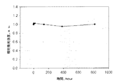
酸化ユーロピウムEu2O3(1.14g、0.65モル%)、3.9gのCaO(7モル%)、0.78gのCaF2(1モル%)、0.115gのMnCO3(0.1モル%)、60.08gのケイ酸(100モル%)、21gのNH4I(14.4モル%)を乾燥粉体の形で混合した。混合した粉体をさらに乾燥窒素中140℃で4時間乾燥した。次いで、粉体を形成ガス中(N2中5%v/vのH2)900℃で1時間焼成した。材料を冷却した後、14gのNH4Iを加え、粉体を再び混合した。混合した粉体を形成ガス中1000℃で1時間焼成した。得られた蛍光体は、(CaSiO3)・(SiO2):Eu2+,Mn2+,I−であった。図3のX線回折パターン(イノケイ酸ウォラストナイト(Wollastonite)、石英、クリソトバライトシリカに関して示される)から明らかなように、シリカSiO2はクリストバライトの形であり、イノケイ酸カルシウムはウォラストナイトの形であった。図1に示すように、蛍光体は、410nmの光の励起で635nmのピークを有する明るい赤色光を発光した。蛍光体を85℃85%相対湿度に露出した長期安定性(耐久性)を図2に示す。
Example 1a
Preparation of CaSiO 3. (SiO 2 ) n : Eu 2+ , Mn 2+ , I Europium oxide Eu 2 O 3 (1.14 g, 0.65 mol%), 3.9 g CaO (7 mol%), 0.78 g Dry powder of CaF 2 (1 mol%), 0.115 g MnCO 3 (0.1 mol%), 60.08 g silicic acid (100 mol%), 21 g NH 4 I (14.4 mol%) Mixed in body shape. The mixed powder was further dried for 4 hours at 140 ° C. in dry nitrogen. Then, (H 2 in N 2 in 5% v / v) powder forming gas and calcined 1 hour at 900 ° C.. After the material was cooled, 14 g NH 4 I was added and the powder was mixed again. The mixed powder was baked for 1 hour at 1000 ° C. in forming gas. The obtained phosphor was (CaSiO 3 ) · (SiO 2 ): Eu 2+ , Mn 2+ , I − . As can be seen from the X-ray diffraction pattern of FIG. 3 (shown for Wollastonite, quartz, chrysovalite silica), silica SiO 2 is in the form of cristobalite and calcium inosilicate is wollastonite. It was the form. As shown in FIG. 1, the phosphor emitted bright red light having a peak of 635 nm upon excitation with light of 410 nm. FIG. 2 shows long-term stability (durability) when the phosphor is exposed to 85 ° C. and 85% relative humidity.
〔実施例1b〜f〕
CaSiO3・(SiO2)n:Eu2+,Mn2+,Iの調製
以下の蛍光体を得るためにEu2+とMn2+の比を変化させたことを除いて、実施例1aの方法を用いた。
[Examples 1b to f]
Preparation of CaSiO 3. (SiO 2 ) n : Eu 2+ , Mn 2+ , I The method of Example 1a was used except that the ratio of Eu 2+ and Mn 2+ was changed to obtain the following phosphors. .

〔実施例2〕
CaSiO3・(SiO2)n:Eu2+,Mn2+,Clの調製
乾燥粉砕によって酸化ユーロピウムEu2O3(1.14g、0.65モル%)、3.9gのCaO(7モル%)、0.78gのCaF2(1モル%)、0.115gのMnCO3(0.1モル%)、60.08gのケイ酸(100モル%)、14gのNH4Cl(26モル%)を混合した。混合した粉体をさらに乾燥窒素中で140℃で4時間乾燥した。次いで、粉体を乾燥窒素中900℃で1時間焼成した。材料を室温まで冷却した後、14gのNH4Clを加え、粉体を再び混合した。混合した粉体を形成ガス中1000℃で1時間焼成した。得られた蛍光体は、CaSiO3・(SiO2)n:Eu2+,Mn2+,Cl−であった。図4に示すように、蛍光体は、410nmの光の励起で422nmと585nmのピークを有する明るい橙赤色光を発光した。
[Example 2]
Preparation of CaSiO 3. (SiO 2 ) n : Eu 2+ , Mn 2+ , Cl Europium oxide Eu 2 O 3 (1.14 g, 0.65 mol%), 3.9 g CaO (7 mol%) by dry grinding, Mixing 0.78 g CaF 2 (1 mol%), 0.115 g MnCO 3 (0.1 mol%), 60.08 g silicic acid (100 mol%), 14 g NH 4 Cl (26 mol%) did. The mixed powder was further dried in dry nitrogen at 140 ° C. for 4 hours. The powder was then fired for 1 hour at 900 ° C. in dry nitrogen. After the material was cooled to room temperature, 14 g of NH 4 Cl was added and the powder was mixed again. The mixed powder was baked for 1 hour at 1000 ° C. in forming gas. The obtained phosphor was CaSiO 3. (SiO 2 ) n : Eu 2+ , Mn 2+ , Cl − . As shown in FIG. 4, the phosphor emitted bright orange-red light having peaks of 422 nm and 585 nm upon excitation with light of 410 nm.
〔実施例3a〕
CaSiO3・(SiO2)n:Eu2+,Iの調製
酸化ユーロピウムEu2O3(1.14g、0.65モル%)、3.9gのCaO(7モル%)、0.78gのCaF2(1モル%)、60.08gのケイ酸(100モル%)、14gのNH4I(9.6モル%)を乾燥粉体の形で混合した。混合した粉体をさらに窒素中で140℃で4時間乾燥した。次いで、粉体を乾燥窒素中900℃で1時間焼成した。材料を冷却した後、14gのNH4Iを加え、再び混合した。混合した粉体を形成ガス中1000℃で1時間焼成した。得られた蛍光体は、(CaSiO3)・(SiO2)n:Eu2+,I−であり、図5に示すように、410nmの光の励起で465nmのピークを有する明るい青色光を発光した。蛍光体は、CaSiO3のウォラストナイトとクリストバライトSiO2を有する多形結晶組成物を示した。耐久性を図6に示す。
Example 3a
Preparation of CaSiO 3. (SiO 2 ) n : Eu 2+ , I Europium oxide Eu 2 O 3 (1.14 g, 0.65 mol%), 3.9 g CaO (7 mol%), 0.78 g CaF 2 (1 mol%), 60.08 g of silicic acid (100 mol%), 14 g of NH 4 I (9.6 mol%) were mixed in the form of a dry powder. The mixed powder was further dried in nitrogen at 140 ° C. for 4 hours. The powder was then fired for 1 hour at 900 ° C. in dry nitrogen. After the material was cooled, 14 g NH 4 I was added and mixed again. The mixed powder was baked for 1 hour at 1000 ° C. in forming gas. The obtained phosphor was (CaSiO 3 ) · (SiO 2 ) n : Eu 2+ , I − , and emitted bright blue light having a peak of 465 nm when excited with light of 410 nm as shown in FIG. . The phosphor showed a polymorphic crystal composition with CaSiO 3 wollastonite and cristobalite SiO 2 . The durability is shown in FIG.
〔実施例3b〜i〕
CaSiO3・(SiO2)n:Eu2+,Iの調製
以下の蛍光体を得るためにEu2+とMn2+の比を変化させたことを除いて、実施例3aの方法を用いた。
[Examples 3b to i]
Preparation of CaSiO 3. (SiO 2 ) n : Eu 2+ , I The method of Example 3a was used except that the ratio of Eu 2+ to Mn 2+ was changed to obtain the following phosphors.
〔実施例4〕
CaSiO3・(SiO2)n:Eu2+,Mn2+,Brの調製
酸化ユーロピウムEu2O3(1.14g、0.65モル%)、3.9gのCaO(9.7モル%)、0.78gのCaF2(1モル%)、0.115gのMnCO3(0.1モル%)、60.08gのケイ酸(100モル%)、16gのNH4Br(16モル%)を粉砕によって混合した。混合した粉体をさらに乾燥窒素中で140℃で4時間乾燥した。次いで、粉体を形成ガス中900℃で1時間焼成した。材料を冷却した後、14gのNH4Brを加え、再び混合した。混合した粉体を形成ガス中1000℃で1時間焼成した。得られた蛍光体は、CaSiO3・(SiO2)n:Eu2+,Mn2+,Br−であり、図7に示すように、400nmの光の励起で明るい青色(430nm)と橙色(584nm)を発光した。
Example 4
Preparation of CaSiO 3. (SiO 2 ) n : Eu 2+ , Mn 2+ , Br Europium oxide Eu 2 O 3 (1.14 g, 0.65 mol%), 3.9 g CaO (9.7 mol%), 0 .78 g CaF 2 (1 mol%), 0.115 g MnCO 3 (0.1 mol%), 60.08 g silicic acid (100 mol%), 16 g NH 4 Br (16 mol%) by grinding Mixed. The mixed powder was further dried in dry nitrogen at 140 ° C. for 4 hours. The powder was then fired for 1 hour at 900 ° C. in forming gas. After the material was cooled, 14 g NH 4 Br was added and mixed again. The mixed powder was baked for 1 hour at 1000 ° C. in forming gas. The obtained phosphors are CaSiO 3 · (SiO 2 ) n : Eu 2+ , Mn 2+ , Br − , and as shown in FIG. 7, bright blue (430 nm) and orange (584 nm) are excited by excitation of 400 nm light. Emitted light.
〔実施例5〕
MgSiO3・(SiO2)n:Eu2+,Mn2+,I−の調製
酸化ユーロピウムEu2O3(1.14g、0.65モル%)、3.9gのMgO(7モル%)、0.115gのMnCO3(0.1モル%)、60.08gのケイ酸(100モル%)、14gのNH4I(15モル%)を乾燥粉体の形で混合した。混合した粉体をさらに乾燥窒素中で140℃で4時間乾燥した。次いで、粉体を形成ガス中900℃で1時間焼成した。材料を冷却した後、14gのNH4Iを加え、再び混合した。混合した粉体を乾燥形成ガス中1000℃で1時間焼成した。得られた蛍光体は、([Mg]SiO3)・(SiO2)n:Eu2+,Mn2+I−であった。図9のX線回折パターン(エンスタライトMgと石英に関して示す)から明らかなように、シリカSiO2はクリストバライトの形に結晶化し、イノケイ酸マグネシウムはエンスタライトの形であった。この回折パターンは、シリカが大部分非晶質であることを示す。この蛍光体は図8に示すように、410nmの光励起によって(430nmで青色、644nmで赤色)発光された。
Example 5
Preparation of MgSiO 3. (SiO 2 ) n: Eu 2+ , Mn 2+ , I − Europium oxide Eu 2 O 3 (1.14 g, 0.65 mol%), 3.9 g MgO (7 mol%), 0. 115 g of MnCO 3 (0.1 mol%), 60.08 g of silicic acid (100 mol%), 14 g of NH 4 I (15 mol%) were mixed in the form of a dry powder. The mixed powder was further dried in dry nitrogen at 140 ° C. for 4 hours. The powder was then fired for 1 hour at 900 ° C. in forming gas. After the material was cooled, 14 g NH 4 I was added and mixed again. The mixed powder was calcined at 1000 ° C. for 1 hour in a dry forming gas. The obtained phosphor was ([Mg] SiO 3 ) · (SiO 2 ) n : Eu 2+ , Mn 2+ I − . As is apparent from the X-ray diffraction pattern of FIG. 9 (shown with respect to enstarlite Mg and quartz), silica SiO 2 crystallized in the form of cristobalite and magnesium inosilicate was in the form of ensterite. This diffraction pattern indicates that the silica is mostly amorphous. As shown in FIG. 8, this phosphor was emitted by light excitation at 410 nm (blue at 430 nm, red at 644 nm).
〔実施例6〕
MgSiO3・(SiO2)n:Eu2+,Mn2+,Br−の調製
酸化ユーロピウムEu2O3(1.14g、0.65モル%)、3.9gのMgO(7モル%)、0.115gのMnCO3(0.1モル%)、60.08gのケイ酸(100モル%)、16gのNH4Br(16.3モル%)を乾燥粉砕によって混合した。混合した粉体をさらに乾燥窒素中で140℃で4時間乾燥した。次いで、粉体を形成ガス中900℃で1時間焼成した。材料を冷却した後、14gのNH4Brを加え、再び混合した。混合した粉体を形成ガス中1000℃で1時間焼成した。得られた蛍光体は、MgSiO3・(SiO2)n:Eu2+,Mn2+Br−であり、図10に示すように、400nmの光励起によって(410nmで青色、475nmで青色、620nmで赤色)を発光した。
Example 6
Preparation of MgSiO 3. (SiO 2 ) n: Eu 2+ , Mn 2+ , Br − Europium oxide Eu 2 O 3 (1.14 g, 0.65 mol%), 3.9 g of MgO (7 mol%), 0. 115 g MnCO 3 (0.1 mol%), 60.08 g silicic acid (100 mol%), 16 g NH 4 Br (16.3 mol%) were mixed by dry grinding. The mixed powder was further dried in dry nitrogen at 140 ° C. for 4 hours. The powder was then fired for 1 hour at 900 ° C. in forming gas. After the material was cooled, 14 g NH 4 Br was added and mixed again. The mixed powder was baked for 1 hour at 1000 ° C. in forming gas. The obtained phosphor is MgSiO 3. (SiO 2 ) n : Eu 2+ , Mn 2+ Br − , as shown in FIG. 10, by photoexcitation at 400 nm (blue at 410 nm, blue at 475 nm, red at 620 nm). Emitted light.
〔実施例7〕
CaSiO3:Eu2+,Mn2+,I−の調製
酸化ユーロピウムEu2O3(1.14g、0.65モル%)、3.9gのCaO(7モル%)、0.78gのCaF2(1モル%)、0.115gのMnCO3(0.1モル%)、60.08gのケイ酸(100モル%)、16gのNH4I(11モル%)を乾燥粉砕によって混合した。混合した粉体をさらに乾燥窒素中で140℃で4時間乾燥した。次いで、粉体を形成ガス中900℃で1時間焼成した。材料を冷却した後、14gのNH4Iを加え、再び混合した。混合した粉体を形成ガス中1000℃で1時間焼成した。得られた蛍光体は、CaSiO3:Eu2+,Mn2+,I−であり、図11に示すように、400nmの光励起によって(460nmで青色、610nmで赤色)を発光した。
Example 7
Preparation of CaSiO 3 : Eu 2+ , Mn 2+ , I − Europium oxide Eu 2 O 3 (1.14 g, 0.65 mol%), 3.9 g CaO (7 mol%), 0.78 g CaF 2 (1 Mol%), 0.115 g MnCO 3 (0.1 mol%), 60.08 g silicic acid (100 mol%), 16 g NH 4 I (11 mol%) were mixed by dry grinding. The mixed powder was further dried in dry nitrogen at 140 ° C. for 4 hours. The powder was then fired for 1 hour at 900 ° C. in forming gas. After the material was cooled, 14 g NH 4 I was added and mixed again. The mixed powder was baked for 1 hour at 1000 ° C. in forming gas. The obtained phosphor was CaSiO 3 : Eu 2+ , Mn 2+ , I − , and emitted light by blue photoexcitation (blue at 460 nm, red at 610 nm) as shown in FIG.
〔実施例8〕
(SiO2)n:Eu2+,Mn2+,I−の調製
酸化ユーロピウムEu2O3(1.14g、0.65モル%)、0.78gのCaF2(1モル%)、0.115gのMnCO3(0.1モル%)、60.08gのケイ酸(100モル%)、16gのNH4I(11モル%)を乾燥粉砕によって混合した。混合した粉体をさらに乾燥窒素中で140℃で4時間乾燥した。次いで、粉体を形成ガス中900℃で1時間焼成した。材料を冷却した後、14gのNH4Brを加え、再び混合した。混合した粉体を形成ガス中1000℃で1時間焼成した。得られた蛍光体は、(SiO2)n:Eu2+,Mn2+,I−であり、図12に示すように、400nmの光励起によって(430nmで青色、640nmで赤色)を発光した。
Example 8
Preparation of (SiO 2 ) n: Eu 2+ , Mn 2+ , I − Europium oxide Eu 2 O 3 (1.14 g, 0.65 mol%), 0.78 g CaF 2 (1 mol%), 0.115 g MnCO 3 (0.1 mol%), 60.08 g silicic acid (100 mol%), 16 g NH 4 I (11 mol%) were mixed by dry grinding. The mixed powder was further dried in dry nitrogen at 140 ° C. for 4 hours. The powder was then fired for 1 hour at 900 ° C. in forming gas. After the material was cooled, 14 g NH 4 Br was added and mixed again. The mixed powder was baked for 1 hour at 1000 ° C. in forming gas. The obtained phosphor was (SiO 2 ) n : Eu 2+ , Mn 2+ , I − , and emitted light by light excitation at 400 nm (blue at 430 nm, red at 640 nm) as shown in FIG.
〔実施例9〕
410nm発光LEDチップおよび第1蛍光体混合物を有する白色光装置の作製
蛍光体混合物を、実施例1で作製した赤色発光金属ケイ酸−シリカ系多形蛍光体CaSiO3・(SiO2)n:Eu2+,Mn2+,I−と、緑色発光蛍光体BaMgAl10O17:Eu2+,Mn2+,(BAM:Eu,Mn)(G)と、実施例3で作製した青色発光蛍光体CaSiO3・(SiO2)n:Eu2+,I−(B)とから作製する。3種の蛍光体を適切な重量比で混合し、さらに蛍光体とエポキシ樹脂を混合してスラリーを形成する。410nmを発光するInGaN系LEDチップ上にスラリーを塗工する。装置は白色の光を発生し、その色彩座標は3種類の蛍光体の比の変化によって変化させることができる。
Example 9
Production of white light device having 410 nm light emitting LED chip and first phosphor mixture Red light emitting metal silicate-silica polymorph phosphor CaSiO 3. (SiO 2 ) n : Eu produced in Example 1 2+ , Mn 2+ , I − , green light emitting phosphor BaMgAl 10 O 17 : Eu 2+ , Mn 2+ , (BAM: Eu, Mn) (G), and blue light emitting phosphor CaSiO 3. It is prepared from SiO 2 ) n : Eu 2+ , I − (B). Three kinds of phosphors are mixed at an appropriate weight ratio, and further, the phosphor and the epoxy resin are mixed to form a slurry. A slurry is applied on an InGaN-based LED chip that emits 410 nm. The device generates white light and its color coordinates can be changed by changing the ratio of the three phosphors.
〔実施例10〕
410nm発光LEDチップおよび第2蛍光体混合物を有する白色光装置の作製
蛍光体混合物を、実施例1で作製した赤色発光金属ケイ酸塩−シリカ系多形蛍光体CaSiO3・(SiO2)n:Eu2+,Mn2+,I−と、緑色発光蛍光体SrGa2S4:Eu2+(STG:Eu)(G)と、実施例3で作製した青色発光蛍光体CaSiO3・(SiO2)n:Eu2+,I−(B)とから作製する。3種の蛍光体を適切な重量比で混合し、さらに蛍光体とエポキシ樹脂を混合してスラリーを形成する。410nmを発光するInGaN系LEDチップ上にスラリーを塗工する。装置は白色の光を発生し、その色彩座標は3種類の蛍光体の比の変化によって変化させることができる。装置構造は図13とすることができる。
Example 10
Production of white light device having 410 nm light emitting LED chip and second phosphor mixture Red light emitting metal silicate-silica-based polymorph phosphor CaSiO 3. (SiO 2 ) n produced in Example 1: Eu 2+ , Mn 2+ , I − , green light emitting phosphor SrGa 2 S 4 : Eu 2+ (STG: Eu) (G), and blue light emitting phosphor CaSiO 3. (SiO 2 ) n produced in Example 3: It is prepared from Eu 2+ and I − (B). Three kinds of phosphors are mixed at an appropriate weight ratio, and further, the phosphor and the epoxy resin are mixed to form a slurry. A slurry is applied on an InGaN-based LED chip that emits 410 nm. The device generates white light and its color coordinates can be changed by changing the ratio of the three phosphors. The device structure can be shown in FIG.
〔実施例11〕
410nm発光LEDチップおよび紫色発光蛍光体を有する紫色光装置の作製
実施例2で作製した単一蛍光体の紫色を発光するCaSiO3・(SiO2)n:Eu2+,Mn2+,Cl−をエポキシ樹脂と混合してスラリーを形成する。410nmを発光するInGaN系LEDチップ上にスラリーを塗工する。装置は紫色の光を発生する。この光の色は、娯楽的な環境におけるある種の照明に適している。
Example 11
Production of a purple light device having a 410 nm light emitting LED chip and a purple light emitting phosphor. CaSiO 3. (SiO 2 ) n : Eu 2+ , Mn 2+ , Cl − which emits purple light of a single phosphor produced in Example 2 is epoxy. Mix with resin to form slurry. A slurry is applied on an InGaN-based LED chip that emits 410 nm. The device emits purple light. This color of light is suitable for certain types of lighting in an entertainment environment.
特許および特許出願を含むがそれだけに限定されない、本明細書に引用された刊行物および参考文献は、引用された全部分においてその全体が参照により本明細書に組み込まれており、あたかも、各個別の刊行物または参考文献が参照によって具体的にかつ個別に本明細書に完全に記載されて組み込まれているかのようになっている。刊行物および参考文献について上述したのと同様、本出願が優先権を主張するいかなる特許出願も、参照により本明細書に組み込まれている。 Publications and references cited herein, including but not limited to patents and patent applications, are hereby incorporated by reference in their entirety in all parts cited, as if each individual It is as if the publications or references were specifically and individually incorporated by reference in their entirety. As described above for publications and references, any patent application to which this application claims priority is incorporated herein by reference.
本発明は好ましい実施形態を強調して説明したが、当業者であれば、好ましい装置と方法の変形を用いることができ、本明細書に具体的に説明された形態以外で本発明を実施できることは明らかであろう。したがって、本発明は、特許請求の範囲によって定義される本発明の精神と範囲内に包含されるすべての修正を含む。 While this invention has been described with emphasis on preferred embodiments, those skilled in the art can use preferred apparatus and method variations and practice the invention in forms other than those specifically described herein. Will be clear. Accordingly, this invention includes all modifications encompassed within the spirit and scope of the invention as defined by the claims.
本出願は2005年3月25日に出願された以下の案件から優先権を主張するものである。米国特許出願第60/665,458号、第60/665,636号、第60/665,456号、第60/665,457号、2005年5月24日出願の米国特許出願第60/684,373号、2005年6月10日出願の米国特許出願第11/149,648号。
This application claims priority from the following cases filed on March 25, 2005.
Claims (17)
前記半導体光源と発光装置によって生成される出力光との間に配置された波長制御体とを含む発光装置であって、
前記波長制御体が、下記式:
(CaSiO3)m・(SiO2)n:Rε,X
(式中、
RεはEu2+イオン及びMn2+イオンから選択される少なくとも1種の活性剤であり、
Xは少なくとも1種のハロゲン化物イオンであり、
mは1であり、及び
nは3よりも大きい)
で表される蛍光体を含む発光装置。 A semiconductor light source that generates output light of a wavelength of at least 300 nm;
A light emitting device including a wavelength control body disposed between the semiconductor light source and output light generated by the light emitting device,
The wavelength control body has the following formula:
(CaSiO 3 ) m · (SiO 2 ) n : Rε, X
(Where
Rε is at least one activator selected from Eu 2+ ions and Mn 2+ ions;
X is at least one halide ion;
m is 1 and n is greater than 3)
A light-emitting device including a phosphor represented by
前記n型クラッド層がAlrGa1−rN(式中、0≦r<1)から形成され、
前記p型クラッド層が前記n型クラッド層のバンドギャップよりも大きなバンドギャップを場合によって有する、請求項7に記載の発光装置。 The p-type cladding layer is formed of Al q Ga 1-q N (where 0 <q <1);
The n-type cladding layer is formed of Al r Ga 1-r N (where 0 ≦ r <1);
The light emitting device according to claim 7, wherein the p-type cladding layer optionally has a band gap larger than that of the n-type cladding layer.
(CaSiO3)m・(SiO2)n:Rε,X
(式中、
RεはEu2+イオン及びMn2+イオンから選択される少なくとも1種の活性剤であり、
Xは少なくとも1種のハロゲン化物イオンであり、
mは1であり、及び
nは3よりも大きい)
で表される蛍光体を製造する方法であって、
a)適切な前駆体を混合する工程、
b)スラリーを形成する工程、
c)前記スラリーを粉砕する工程、
d)前記スラリーを乾燥する工程、
e)前記スラリーを還元ガス中第1温度で加熱する工程、
f)Xの前駆体をさらに混合する工程、
g)第1温度よりも高い第2温度で、工程b)〜f)のいずれかを還元ガス中で焼成し、生成物を生成する工程、
h)工程g)の生成物を洗浄する工程、および
i)場合によって、工程h)の生成物に後形成処理を適用する工程、
を有する方法。 Following formula:
(CaSiO 3 ) m · (SiO 2 ) n : Rε, X
(Where
Rε is at least one activator selected from Eu 2+ ions and Mn 2+ ions;
X is at least one halide ion;
m is 1 and n is greater than 3)
A method for producing a phosphor represented by:
a) mixing a suitable precursor;
b) forming a slurry;
c) crushing the slurry;
d) drying the slurry;
e) heating the slurry in a reducing gas at a first temperature;
f) further mixing the precursor of X;
g) a step of firing any of steps b) to f) in a reducing gas at a second temperature higher than the first temperature to produce a product;
h) washing the product of step g), and i) optionally applying a post-formation treatment to the product of step h),
Having a method.
Applications Claiming Priority (12)
| Application Number | Priority Date | Filing Date | Title |
|---|---|---|---|
| US66563605P | 2005-03-25 | 2005-03-25 | |
| US66545605P | 2005-03-25 | 2005-03-25 | |
| US66545705P | 2005-03-25 | 2005-03-25 | |
| US66545805P | 2005-03-25 | 2005-03-25 | |
| US60/665457 | 2005-03-25 | ||
| US60/665458 | 2005-03-25 | ||
| US60/665456 | 2005-03-25 | ||
| US60/665636 | 2005-03-25 | ||
| US68437305P | 2005-05-24 | 2005-05-24 | |
| US60/684373 | 2005-05-24 | ||
| US11/149648 | 2005-06-10 | ||
| US11/149,648 US7276183B2 (en) | 2005-03-25 | 2005-06-10 | Metal silicate-silica-based polymorphous phosphors and lighting devices |
Publications (3)
| Publication Number | Publication Date |
|---|---|
| JP2006274263A JP2006274263A (en) | 2006-10-12 |
| JP2006274263A5 JP2006274263A5 (en) | 2007-10-11 |
| JP5209850B2 true JP5209850B2 (en) | 2013-06-12 |
Family
ID=37034318
Family Applications (1)
| Application Number | Title | Priority Date | Filing Date |
|---|---|---|---|
| JP2006082970A Expired - Fee Related JP5209850B2 (en) | 2005-03-25 | 2006-03-24 | Metal silicate-silica polymorph phosphor and light emitting device |
Country Status (7)
| Country | Link |
|---|---|
| US (1) | US7276183B2 (en) |
| EP (1) | EP1861884B1 (en) |
| JP (1) | JP5209850B2 (en) |
| KR (1) | KR101255846B1 (en) |
| AT (1) | ATE521991T1 (en) |
| TW (1) | TWI413275B (en) |
| WO (1) | WO2006104860A2 (en) |
Families Citing this family (27)
| Publication number | Priority date | Publication date | Assignee | Title |
|---|---|---|---|---|
| US20070051924A1 (en) * | 2005-09-07 | 2007-03-08 | Canon Kabushiki Kaisha | Fluorescent material, fluorescent substance, display, and process for preparing fluorescent substance |
| KR100724591B1 (en) * | 2005-09-30 | 2007-06-04 | 서울반도체 주식회사 | Light emitting device and LCD backlight using the same |
| US8906262B2 (en) * | 2005-12-02 | 2014-12-09 | Lightscape Materials, Inc. | Metal silicate halide phosphors and LED lighting devices using the same |
| EP2003183B1 (en) * | 2006-03-10 | 2012-08-29 | Kabushiki Kaisha Toshiba | Phosphor and light-emitting device |
| US8323529B2 (en) * | 2006-03-16 | 2012-12-04 | Seoul Semiconductor Co., Ltd. | Fluorescent material and light emitting diode using the same |
| CN101605867B (en) * | 2006-10-03 | 2013-05-08 | 渲染材料公司 | Metal silicate halide phosphors and led lighting devices using the same |
| JP2008177484A (en) * | 2007-01-22 | 2008-07-31 | Central Glass Co Ltd | Visible light-emitting material and visible light-emitting device |
| JP5222600B2 (en) * | 2007-04-05 | 2013-06-26 | 株式会社小糸製作所 | Phosphor |
| DE102008017039A1 (en) * | 2007-04-05 | 2008-10-09 | Koito Manufacturing Co., Ltd. | fluorescent |
| JP5094246B2 (en) * | 2007-07-06 | 2012-12-12 | 株式会社日立製作所 | Plasma display device |
| EP2015614B1 (en) * | 2007-07-12 | 2010-12-15 | Koito Manufacturing Co., Ltd. | Light emitting device |
| US8436526B2 (en) * | 2008-02-11 | 2013-05-07 | Sensor Electronic Technology, Inc. | Multiwavelength solid-state lamps with an enhanced number of rendered colors |
| US7990045B2 (en) * | 2008-03-15 | 2011-08-02 | Sensor Electronic Technology, Inc. | Solid-state lamps with partial conversion in phosphors for rendering an enhanced number of colors |
| US20090231832A1 (en) * | 2008-03-15 | 2009-09-17 | Arturas Zukauskas | Solid-state lamps with complete conversion in phosphors for rendering an enhanced number of colors |
| WO2009143283A1 (en) * | 2008-05-20 | 2009-11-26 | Lightscape Materials, Inc. | Silicate-based phosphors and led lighting devices using the same |
| US8592829B2 (en) * | 2009-08-17 | 2013-11-26 | Osram Sylvania Inc. | Phosphor blend for an LED light source and LED light source incorporating same |
| TWI361216B (en) * | 2009-09-01 | 2012-04-01 | Ind Tech Res Inst | Phosphors, fabricating method thereof, and light emitting device employing the same |
| CN103068952A (en) | 2010-08-26 | 2013-04-24 | 默克专利有限公司 | Silicate-based phosphor |
| WO2012073887A1 (en) * | 2010-11-30 | 2012-06-07 | パナソニック株式会社 | Phosphor and light emitting device |
| US8801969B2 (en) * | 2011-01-14 | 2014-08-12 | Lightscape Materials, Inc. | Carbonitride and carbidonitride phosphors and lighting devices using the same |
| EP2677017A4 (en) * | 2011-02-14 | 2015-08-19 | Koito Mfg Co Ltd | Method for producing fluorescent substance |
| CN103078044A (en) * | 2013-01-09 | 2013-05-01 | 宏齐光电子(深圳)有限公司 | Production method of ultrasmall-sized red-green-blue (RGB) full-color light emitting diode (LED) for high-definition display screen |
| CN103762298A (en) * | 2014-02-02 | 2014-04-30 | 芜湖市神龙新能源科技有限公司 | LED wafer combination package material and technology |
| US9315725B2 (en) * | 2014-08-28 | 2016-04-19 | Lightscape Materials, Inc. | Method of making EU2+ activated inorganic red phosphor |
| JP6728233B2 (en) * | 2015-04-27 | 2020-07-22 | メルク パテント ゲゼルシャフト ミット ベシュレンクテル ハフツングMerck Patent Gesellschaft mit beschraenkter Haftung | Silicate phosphor |
| EP3435429B1 (en) * | 2016-03-24 | 2022-10-26 | Sony Group Corporation | Light emitting device, display apparatus, and illumination apparatus |
| JP6885405B2 (en) * | 2016-08-24 | 2021-06-16 | 堺化学工業株式会社 | Fluorescent material and resin composition containing it |
Family Cites Families (111)
| Publication number | Priority date | Publication date | Assignee | Title |
|---|---|---|---|---|
| GB864343A (en) * | 1956-07-06 | 1961-04-06 | Ass Elect Ind | Improvements in luminescent materials |
| GB1087655A (en) * | 1965-04-14 | 1967-10-18 | Gen Electric Co Ltd | Improvements in or relating to luminescent materials |
| DE10028266A1 (en) | 2000-06-09 | 2001-12-13 | Patent Treuhand Ges Fuer Elektrische Gluehlampen Mbh | Luminescent material used for emitting green light is of the thiogallate class |
| US3790490A (en) | 1971-03-03 | 1974-02-05 | Gen Electric | Europium and manganese activated strontium chlorosilicate phosphor |
| JPS57166529A (en) | 1981-04-07 | 1982-10-14 | Omron Tateisi Electronics Co | Method and device for measuring temperature |
| US5140163A (en) * | 1987-08-17 | 1992-08-18 | Agfa-Gevaert, N.V. | Reproduction of X-ray images with photostimulable phosphor |
| US5472636A (en) * | 1994-09-14 | 1995-12-05 | Osram Sylvania Inc. | Method of preparing manganese and lead coactivated calcium silicate phosphor |
| DE19638667C2 (en) | 1996-09-20 | 2001-05-17 | Osram Opto Semiconductors Gmbh | Mixed-color light-emitting semiconductor component with luminescence conversion element |
| TW383508B (en) | 1996-07-29 | 2000-03-01 | Nichia Kagaku Kogyo Kk | Light emitting device and display |
| KR20000070747A (en) | 1997-02-03 | 2000-11-25 | 에프. 아. 프라저, 에른스트 알테르 (에. 알테르), 한스 페터 비틀린 (하. 페. 비틀린), 피. 랍 보프, 브이. 스펜글러, 페. 아에글러 | Process for the preparation of fluorescent compositions, fluorescent compositions and their use |
| JP2000509912A (en) | 1997-03-03 | 2000-08-02 | コーニンクレッカ フィリップス エレクトロニクス エヌ ヴィ | White light emitting diode |
| US5958591A (en) | 1997-06-30 | 1999-09-28 | Minnesota Mining And Manufacturing Company | Electroluminescent phosphor particles encapsulated with an aluminum oxide based multiple oxide coating |
| US6294800B1 (en) | 1998-02-06 | 2001-09-25 | General Electric Company | Phosphors for white light generation from UV emitting diodes |
| US6252254B1 (en) | 1998-02-06 | 2001-06-26 | General Electric Company | Light emitting device with phosphor composition |
| US6278135B1 (en) | 1998-02-06 | 2001-08-21 | General Electric Company | Green-light emitting phosphors and light sources using the same |
| US6255670B1 (en) | 1998-02-06 | 2001-07-03 | General Electric Company | Phosphors for light generation from light emitting semiconductors |
| JP2002520822A (en) | 1998-06-30 | 2002-07-09 | オスラム オプト セミコンダクターズ ゲゼルシャフト ミット ベシュレンクテル ハフツング ウント コンパニー オッフェネ ハンデルスゲゼルシャフト | Light source that generates visible light |
| JP4399518B2 (en) * | 1998-07-16 | 2010-01-20 | 三菱化学株式会社 | Phosphor for vacuum ultraviolet ray, method for producing the same, phosphor paste composition, and vacuum ultraviolet light emitting device |
| US5959316A (en) | 1998-09-01 | 1999-09-28 | Hewlett-Packard Company | Multiple encapsulation of phosphor-LED devices |
| WO2000019546A1 (en) | 1998-09-28 | 2000-04-06 | Koninklijke Philips Electronics N.V. | Lighting system |
| US6366018B1 (en) | 1998-10-21 | 2002-04-02 | Sarnoff Corporation | Apparatus for performing wavelength-conversion using phosphors with light emitting diodes |
| US6299338B1 (en) * | 1998-11-30 | 2001-10-09 | General Electric Company | Decorative lighting apparatus with light source and luminescent material |
| US6429583B1 (en) | 1998-11-30 | 2002-08-06 | General Electric Company | Light emitting device with ba2mgsi2o7:eu2+, ba2sio4:eu2+, or (srxcay ba1-x-y)(a1zga1-z)2sr:eu2+phosphors |
| US6373188B1 (en) | 1998-12-22 | 2002-04-16 | Honeywell International Inc. | Efficient solid-state light emitting device with excited phosphors for producing a visible light output |
| TW498102B (en) | 1998-12-28 | 2002-08-11 | Futaba Denshi Kogyo Kk | A process for preparing GaN fluorescent substance |
| US6273589B1 (en) | 1999-01-29 | 2001-08-14 | Agilent Technologies, Inc. | Solid state illumination source utilizing dichroic reflectors |
| US6212213B1 (en) | 1999-01-29 | 2001-04-03 | Agilent Technologies, Inc. | Projector light source utilizing a solid state green light source |
| US6351069B1 (en) | 1999-02-18 | 2002-02-26 | Lumileds Lighting, U.S., Llc | Red-deficiency-compensating phosphor LED |
| US6155699A (en) | 1999-03-15 | 2000-12-05 | Agilent Technologies, Inc. | Efficient phosphor-conversion led structure |
| TW455908B (en) | 1999-04-20 | 2001-09-21 | Koninkl Philips Electronics Nv | Lighting system |
| US6811813B1 (en) | 1999-05-19 | 2004-11-02 | Sarnoff Corporation | Method of coating micrometer sized inorganic particles |
| EP1142033A1 (en) | 1999-09-27 | 2001-10-10 | LumiLeds Lighting U.S., LLC | A light emitting diode device that produces white light by performing complete phosphor conversion |
| US6686691B1 (en) | 1999-09-27 | 2004-02-03 | Lumileds Lighting, U.S., Llc | Tri-color, white light LED lamps |
| US6696703B2 (en) | 1999-09-27 | 2004-02-24 | Lumileds Lighting U.S., Llc | Thin film phosphor-converted light emitting diode device |
| DE19952932C1 (en) | 1999-11-03 | 2001-05-03 | Osram Opto Semiconductors Gmbh | LED white light source with broadband excitation |
| EP1104799A1 (en) | 1999-11-30 | 2001-06-06 | Patent-Treuhand-Gesellschaft für elektrische Glühlampen mbH | Red emitting luminescent material |
| US6513949B1 (en) | 1999-12-02 | 2003-02-04 | Koninklijke Philips Electronics N.V. | LED/phosphor-LED hybrid lighting systems |
| DE10001189A1 (en) | 2000-01-14 | 2001-07-19 | Philips Corp Intellectual Pty | Liquid crystal color picture screen has liquid crystal layer between substrate with blue radiation source, e.g. blue-light-emitting diode and substrate with phosphor layer |
| JP4406490B2 (en) | 2000-03-14 | 2010-01-27 | 株式会社朝日ラバー | Light emitting diode |
| TW480744B (en) | 2000-03-14 | 2002-03-21 | Lumileds Lighting Bv | Light-emitting diode, lighting device and method of manufacturing same |
| US6603258B1 (en) | 2000-04-24 | 2003-08-05 | Lumileds Lighting, U.S. Llc | Light emitting diode device that emits white light |
| US6501100B1 (en) | 2000-05-15 | 2002-12-31 | General Electric Company | White light emitting phosphor blend for LED devices |
| US6621211B1 (en) | 2000-05-15 | 2003-09-16 | General Electric Company | White light emitting phosphor blends for LED devices |
| DE10026435A1 (en) | 2000-05-29 | 2002-04-18 | Osram Opto Semiconductors Gmbh | Calcium-magnesium-chlorosilicate phosphor and its application in luminescence conversion LEDs |
| EP1206802B1 (en) | 2000-05-29 | 2008-03-19 | Patent-Treuhand-Gesellschaft für elektrische Glühlampen mbH | Led-based white-light emitting lighting unit |
| US6577073B2 (en) | 2000-05-31 | 2003-06-10 | Matsushita Electric Industrial Co., Ltd. | Led lamp |
| US6850002B2 (en) | 2000-07-28 | 2005-02-01 | Osram Opto Semiconductors Gmbh | Light emitting device for generating specific colored light, including white light |
| DE10036940A1 (en) | 2000-07-28 | 2002-02-07 | Patent Treuhand Ges Fuer Elektrische Gluehlampen Mbh | Luminescence conversion LED |
| US6544438B2 (en) | 2000-08-02 | 2003-04-08 | Sarnoff Corporation | Preparation of high emission efficiency alkaline earth metal thiogallate phosphors |
| AT410266B (en) | 2000-12-28 | 2003-03-25 | Tridonic Optoelectronics Gmbh | LIGHT SOURCE WITH A LIGHT-EMITTING ELEMENT |
| US6417019B1 (en) | 2001-04-04 | 2002-07-09 | Lumileds Lighting, U.S., Llc | Phosphor converted light emitting diode |
| US6685852B2 (en) | 2001-04-27 | 2004-02-03 | General Electric Company | Phosphor blends for generating white light from near-UV/blue light-emitting devices |
| US6616862B2 (en) | 2001-05-21 | 2003-09-09 | General Electric Company | Yellow light-emitting halophosphate phosphors and light sources incorporating the same |
| US6596195B2 (en) | 2001-06-01 | 2003-07-22 | General Electric Company | Broad-spectrum terbium-containing garnet phosphors and white-light sources incorporating the same |
| US6632379B2 (en) | 2001-06-07 | 2003-10-14 | National Institute For Materials Science | Oxynitride phosphor activated by a rare earth element, and sialon type phosphor |
| FR2826016B1 (en) | 2001-06-13 | 2004-07-23 | Rhodia Elect & Catalysis | COMPOUND BASED ON AN ALKALINE EARTH, SULFUR AND ALUMINUM, GALLIUM OR INDIUM, METHOD FOR PREPARING SAME AND USE THEREOF AS LUMINOPHORE |
| JP3749243B2 (en) | 2001-09-03 | 2006-02-22 | 松下電器産業株式会社 | Semiconductor light emitting device, light emitting apparatus, and method for manufacturing semiconductor light emitting device |
| DE10147040A1 (en) | 2001-09-25 | 2003-04-24 | Patent Treuhand Ges Fuer Elektrische Gluehlampen Mbh | Lighting unit with at least one LED as a light source |
| US7294956B2 (en) | 2001-10-01 | 2007-11-13 | Matsushita Electric Industrial Co., Ltd. | Semiconductor light emitting element and light emitting device using this |
| JP2005509081A (en) | 2001-11-14 | 2005-04-07 | サーノフ・コーポレーション | Photo-excited luminescent red phosphor |
| SG173925A1 (en) * | 2002-03-22 | 2011-09-29 | Nichia Corp | Nitride phosphor and production process thereof, and light emitting device |
| US6735467B2 (en) * | 2002-04-15 | 2004-05-11 | Persyst Development Corporation | Method and system for detecting seizures using electroencephalograms |
| JP2003306674A (en) | 2002-04-15 | 2003-10-31 | Sumitomo Chem Co Ltd | Fluorescent material for white led, and white led using the same |
| US20030222268A1 (en) | 2002-05-31 | 2003-12-04 | Yocom Perry Niel | Light sources having a continuous broad emission wavelength and phosphor compositions useful therefor |
| TW563261B (en) | 2002-06-07 | 2003-11-21 | Solidlite Corp | A method and of manufacture for tri-color white LED |
| US6809471B2 (en) | 2002-06-28 | 2004-10-26 | General Electric Company | Phosphors containing oxides of alkaline-earth and Group-IIIB metals and light sources incorporating the same |
| US7768189B2 (en) * | 2004-08-02 | 2010-08-03 | Lumination Llc | White LEDs with tunable CRI |
| US7224000B2 (en) | 2002-08-30 | 2007-05-29 | Lumination, Llc | Light emitting diode component |
| US7800121B2 (en) * | 2002-08-30 | 2010-09-21 | Lumination Llc | Light emitting diode component |
| US20050218781A1 (en) | 2002-09-09 | 2005-10-06 | Hsing Chen | Triple wavelengths light emitting diode |
| US20050218780A1 (en) | 2002-09-09 | 2005-10-06 | Hsing Chen | Method for manufacturing a triple wavelengths white LED |
| JP4225083B2 (en) * | 2002-09-24 | 2009-02-18 | 日亜化学工業株式会社 | Phosphor |
| EP1413618A1 (en) | 2002-09-24 | 2004-04-28 | Osram Opto Semiconductors GmbH | Luminescent material, especially for LED application |
| EP1413619A1 (en) * | 2002-09-24 | 2004-04-28 | Osram Opto Semiconductors GmbH | Luminescent material, especially for LED application |
| JP4263453B2 (en) | 2002-09-25 | 2009-05-13 | パナソニック株式会社 | Inorganic oxide and light emitting device using the same |
| US6717353B1 (en) | 2002-10-14 | 2004-04-06 | Lumileds Lighting U.S., Llc | Phosphor converted light emitting device |
| US20040159900A1 (en) | 2003-01-27 | 2004-08-19 | 3M Innovative Properties Company | Phosphor based light sources having front illumination |
| US20040145312A1 (en) | 2003-01-27 | 2004-07-29 | 3M Innovative Properties Company | Phosphor based light source having a flexible short pass reflector |
| US7091661B2 (en) | 2003-01-27 | 2006-08-15 | 3M Innovative Properties Company | Phosphor based light sources having a reflective polarizer |
| US7210977B2 (en) | 2003-01-27 | 2007-05-01 | 3M Innovative Properties Comapny | Phosphor based light source component and method of making |
| US7118438B2 (en) | 2003-01-27 | 2006-10-10 | 3M Innovative Properties Company | Methods of making phosphor based light sources having an interference reflector |
| US7245072B2 (en) | 2003-01-27 | 2007-07-17 | 3M Innovative Properties Company | Phosphor based light sources having a polymeric long pass reflector |
| US7312560B2 (en) | 2003-01-27 | 2007-12-25 | 3M Innovative Properties | Phosphor based light sources having a non-planar long pass reflector and method of making |
| US7091653B2 (en) | 2003-01-27 | 2006-08-15 | 3M Innovative Properties Company | Phosphor based light sources having a non-planar long pass reflector |
| US6982523B2 (en) | 2003-01-28 | 2006-01-03 | Kabushiki Kaisha Fine Rubber Kenkyuusho | Red light emitting phosphor, its production and light emitting device |
| KR100511562B1 (en) | 2003-01-29 | 2005-09-02 | 한국화학연구원 | Composition and Preparation method of yellow silicates phosphor for white LED and AM LCD |
| US6936857B2 (en) | 2003-02-18 | 2005-08-30 | Gelcore, Llc | White light LED device |
| US7018565B2 (en) | 2003-03-04 | 2006-03-28 | Sarnoff Corporation | Efficient, size-selected green-emitting phosphors |
| US7125501B2 (en) | 2003-04-21 | 2006-10-24 | Sarnoff Corporation | High efficiency alkaline earth metal thiogallate-based phosphors |
| US7368179B2 (en) | 2003-04-21 | 2008-05-06 | Sarnoff Corporation | Methods and devices using high efficiency alkaline earth metal thiogallate-based phosphors |
| KR100573858B1 (en) * | 2003-05-09 | 2006-05-03 | 서울반도체 주식회사 | Luminescence conversion light emitting diode comprising the sialon-based phosphors |
| US6982045B2 (en) | 2003-05-17 | 2006-01-03 | Phosphortech Corporation | Light emitting device having silicate fluorescent phosphor |
| US7250715B2 (en) | 2004-02-23 | 2007-07-31 | Philips Lumileds Lighting Company, Llc | Wavelength converted semiconductor light emitting devices |
| JP2005272831A (en) * | 2004-02-27 | 2005-10-06 | Sumitomo Chemical Co Ltd | Method for producing silicate phosphor |
| US7573072B2 (en) | 2004-03-10 | 2009-08-11 | Lumination Llc | Phosphor and blends thereof for use in LEDs |
| CN1677702A (en) | 2004-03-29 | 2005-10-05 | 斯坦雷电气株式会社 | Light emitting diode |
| US7488990B2 (en) | 2004-04-02 | 2009-02-10 | Avago Technologies Ecbu Ip (Singapore) Pte. Ltd. | Using multiple types of phosphor in combination with a light emitting device |
| KR100605211B1 (en) * | 2004-04-07 | 2006-07-31 | 엘지이노텍 주식회사 | Phosphor and white led using the same |
| US7229573B2 (en) | 2004-04-20 | 2007-06-12 | Gelcore, Llc | Ce3+ and Eu2+ doped phosphors for light generation |
| EP1769050B1 (en) | 2004-07-06 | 2013-01-16 | Lightscape Materials Inc. | Efficient, green-emitting phosphors, and combinations with red-emitting phosphors |
| US20060181192A1 (en) * | 2004-08-02 | 2006-08-17 | Gelcore | White LEDs with tailorable color temperature |
| US7453195B2 (en) * | 2004-08-02 | 2008-11-18 | Lumination Llc | White lamps with enhanced color contrast |
| US7575697B2 (en) * | 2004-08-04 | 2009-08-18 | Intematix Corporation | Silicate-based green phosphors |
| US7390437B2 (en) * | 2004-08-04 | 2008-06-24 | Intematix Corporation | Aluminate-based blue phosphors |
| US7267787B2 (en) * | 2004-08-04 | 2007-09-11 | Intematix Corporation | Phosphor systems for a white light emitting diode (LED) |
| US7311858B2 (en) * | 2004-08-04 | 2007-12-25 | Intematix Corporation | Silicate-based yellow-green phosphors |
| US20060027785A1 (en) * | 2004-08-04 | 2006-02-09 | Intematix Corporation | Novel silicate-based yellow-green phosphors |
| US20060049414A1 (en) * | 2004-08-19 | 2006-03-09 | Chandran Ramachandran G | Novel oxynitride phosphors |
| KR100638619B1 (en) * | 2004-09-23 | 2006-10-26 | 삼성전기주식회사 | Phosphor blends for converting wavelength and light emitting device using the same |
| US8906262B2 (en) * | 2005-12-02 | 2014-12-09 | Lightscape Materials, Inc. | Metal silicate halide phosphors and LED lighting devices using the same |
| JP2007217605A (en) * | 2006-02-17 | 2007-08-30 | Matsushita Electric Works Ltd | Phosphor and process for producing the same, and light emitting device |
-
2005
- 2005-06-10 US US11/149,648 patent/US7276183B2/en active Active
-
2006
- 2006-03-23 KR KR1020077024072A patent/KR101255846B1/en active IP Right Grant
- 2006-03-23 EP EP06739451A patent/EP1861884B1/en not_active Not-in-force
- 2006-03-23 AT AT06739451T patent/ATE521991T1/en not_active IP Right Cessation
- 2006-03-23 WO PCT/US2006/010659 patent/WO2006104860A2/en active Application Filing
- 2006-03-24 TW TW095110458A patent/TWI413275B/en not_active IP Right Cessation
- 2006-03-24 JP JP2006082970A patent/JP5209850B2/en not_active Expired - Fee Related
Also Published As
| Publication number | Publication date |
|---|---|
| EP1861884B1 (en) | 2011-08-24 |
| WO2006104860A3 (en) | 2006-12-21 |
| US7276183B2 (en) | 2007-10-02 |
| KR20070116130A (en) | 2007-12-06 |
| EP1861884A2 (en) | 2007-12-05 |
| WO2006104860A2 (en) | 2006-10-05 |
| EP1861884A4 (en) | 2009-11-25 |
| KR101255846B1 (en) | 2013-04-17 |
| JP2006274263A (en) | 2006-10-12 |
| ATE521991T1 (en) | 2011-09-15 |
| TW200711172A (en) | 2007-03-16 |
| US20060214175A1 (en) | 2006-09-28 |
| TWI413275B (en) | 2013-10-21 |
Similar Documents
| Publication | Publication Date | Title |
|---|---|---|
| JP5209850B2 (en) | Metal silicate-silica polymorph phosphor and light emitting device | |
| JP4283336B2 (en) | Phosphor and production method therefor, phosphor-containing composition, light emitting device, image display device and lighting device | |
| JP5190475B2 (en) | Phosphor and light emitting device using the same | |
| US7713442B2 (en) | Metal silicate halide phosphors and LED lighting devices using the same | |
| US7615797B2 (en) | Phosphor composition and method for producing the same, and light-emitting device using the same | |
| US7432642B2 (en) | Semiconductor light emitting device provided with a light conversion element using a haloborate phosphor composition | |
| US7733002B2 (en) | Semiconductor light emitting device provided with an alkaline earth metal boric halide phosphor for luminescence conversion | |
| US20060017041A1 (en) | Nitride phosphors and devices | |
| WO2007018260A1 (en) | Phosphor and light-emitting device using same | |
| JP2006299168A (en) | Fluorescent substance and light-emitting device using the same | |
| US11005010B2 (en) | Phosphor and method of manufacturing same, and LED lamp | |
| KR101176212B1 (en) | Alkali-earth Phosporus Nitride system phosphor, manufacturing method thereof and light emitting devices using the same | |
| JP2010196049A (en) | Phosphor and method for producing the same, phosphor-containing composition, and light-emitting device, image display device and lighting device using the phosphor | |
| TWI394827B (en) | Phosphors and white light illumination devices utilizing the same | |
| JP2006104413A (en) | Phosphor and white light emitting device using the same | |
| JP4863794B2 (en) | Wavelength converting material, method for producing the same, and light emitting device using the same | |
| CN100555658C (en) | Metal silicate-silica-based polymorphous phosphors and light-emitting device | |
| KR101589226B1 (en) | Phosphor and manufacturing method of the same, and light emitting device using the same | |
| KR100735314B1 (en) | Strontium and calcium thiogallate phosphor and light emitting device using the same |
Legal Events
| Date | Code | Title | Description |
|---|---|---|---|
| A521 | Request for written amendment filed |
Free format text: JAPANESE INTERMEDIATE CODE: A523 Effective date: 20070824 |
|
| A621 | Written request for application examination |
Free format text: JAPANESE INTERMEDIATE CODE: A621 Effective date: 20090323 |
|
| A711 | Notification of change in applicant |
Free format text: JAPANESE INTERMEDIATE CODE: A711 Effective date: 20091030 |
|
| A977 | Report on retrieval |
Free format text: JAPANESE INTERMEDIATE CODE: A971007 Effective date: 20120130 |
|
| A131 | Notification of reasons for refusal |
Free format text: JAPANESE INTERMEDIATE CODE: A131 Effective date: 20120206 |
|
| A601 | Written request for extension of time |
Free format text: JAPANESE INTERMEDIATE CODE: A601 Effective date: 20120502 |
|
| A602 | Written permission of extension of time |
Free format text: JAPANESE INTERMEDIATE CODE: A602 Effective date: 20120509 |
|
| A521 | Request for written amendment filed |
Free format text: JAPANESE INTERMEDIATE CODE: A523 Effective date: 20120803 |
|
| A131 | Notification of reasons for refusal |
Free format text: JAPANESE INTERMEDIATE CODE: A131 Effective date: 20121004 |
|
| A521 | Request for written amendment filed |
Free format text: JAPANESE INTERMEDIATE CODE: A523 Effective date: 20121228 |
|
| TRDD | Decision of grant or rejection written | ||
| A01 | Written decision to grant a patent or to grant a registration (utility model) |
Free format text: JAPANESE INTERMEDIATE CODE: A01 Effective date: 20130124 |
|
| RD02 | Notification of acceptance of power of attorney |
Free format text: JAPANESE INTERMEDIATE CODE: A7422 Effective date: 20130124 |
|
| A61 | First payment of annual fees (during grant procedure) |
Free format text: JAPANESE INTERMEDIATE CODE: A61 Effective date: 20130222 |
|
| FPAY | Renewal fee payment (event date is renewal date of database) |
Free format text: PAYMENT UNTIL: 20160301 Year of fee payment: 3 |
|
| R150 | Certificate of patent or registration of utility model |
Ref document number: 5209850 Country of ref document: JP Free format text: JAPANESE INTERMEDIATE CODE: R150 Free format text: JAPANESE INTERMEDIATE CODE: R150 |
|
| R250 | Receipt of annual fees |
Free format text: JAPANESE INTERMEDIATE CODE: R250 |
|
| R250 | Receipt of annual fees |
Free format text: JAPANESE INTERMEDIATE CODE: R250 |
|
| R250 | Receipt of annual fees |
Free format text: JAPANESE INTERMEDIATE CODE: R250 |
|
| R250 | Receipt of annual fees |
Free format text: JAPANESE INTERMEDIATE CODE: R250 |
|
| LAPS | Cancellation because of no payment of annual fees |