JP4863794B2 - Wavelength converting material, method for producing the same, and light emitting device using the same - Google Patents
Wavelength converting material, method for producing the same, and light emitting device using the same Download PDFInfo
- Publication number
- JP4863794B2 JP4863794B2 JP2006186908A JP2006186908A JP4863794B2 JP 4863794 B2 JP4863794 B2 JP 4863794B2 JP 2006186908 A JP2006186908 A JP 2006186908A JP 2006186908 A JP2006186908 A JP 2006186908A JP 4863794 B2 JP4863794 B2 JP 4863794B2
- Authority
- JP
- Japan
- Prior art keywords
- phosphor
- light
- light emitting
- emitting device
- wavelength
- Prior art date
- Legal status (The legal status is an assumption and is not a legal conclusion. Google has not performed a legal analysis and makes no representation as to the accuracy of the status listed.)
- Expired - Fee Related
Links
Images


Abstract
Description
本発明は、近紫外励起により青から赤の範囲の発光を示す新規な波長変換材料に関する。 The present invention relates to a novel wavelength conversion material that emits light in a blue to red range by near-ultraviolet excitation.
SiAlON蛍光体は、主として窒化珪素や窒化アルミニウムを原料として焼成された蛍光体で、結晶構造を構成する主元素である珪素Si、アルミニウムAl、酸素Oおよび窒素Nの比率の異なる種々の型のものが知られている。そのうちα‐SiAlON蛍光体およびβ‐SiAlON蛍光体は、波長変換材料としてLED等への応用例が報告されている。例えば、特許文献1には、青色発光ダイオードを光源とする白色発光ダイオードに用いるSiAlON蛍光体として、一般式LixMyLnzSi12-(m+n)Al(m+n)OnN16-n(MはCa、Mg、Yの少なくとも1種。Lnは少なくとも1種のランタニド)で表されるα‐SiAlON蛍光体が提案されている。このα‐SiAlON蛍光体の発光ピークは、波長560nm〜590nm程度であり色は黄色となる。また特許文献2には、β‐SiAlON蛍光体として、β型Si3N4結晶構造を持ち、一般式MaSib1Alb2Oc1Nc2(MはMn、Ce、Euから選ばれる1種または2種以上)で表される緑色蛍光体が提案されている。このβ‐SiAlON蛍光体は発光波長500nm〜600nmにピークを持つ。
SiAlON phosphors are phosphors fired mainly from silicon nitride or aluminum nitride, and are of various types with different ratios of silicon Si, aluminum Al, oxygen O and nitrogen N, which are the main elements constituting the crystal structure. It has been known. Of these, α-SiAlON phosphors and β-SiAlON phosphors have been reported to be applied to LEDs and the like as wavelength conversion materials. For example,
さらに特許文献3には、構造MSiONのオキシニトリドや、構造MSiAl2O3N2、M13Si18Al12O18N36、MSi5Al2ON9、M3Si5AlON10のサイアロンなどの蛍光体(これら構造においてカチオンMは部分的にEu、Ceで置き換えられている)を用いたLEDが開示されている。
SiAlONは、結晶格子の堅牢さから、耐熱性に優れる蛍光体となるが、青色のものの報告例は少ない。青色発光蛍光体として広く用いられるバリウムマグネシウムアルミネート蛍光体(以下BAM蛍光体)は、高効率の青色発光が得られるが、耐熱性に問題がある。
Further,
SiAlON is a phosphor with excellent heat resistance due to the robustness of the crystal lattice, but there are few reports of blue ones. A barium magnesium aluminate phosphor (hereinafter referred to as a BAM phosphor) widely used as a blue light-emitting phosphor can obtain a high-efficiency blue light emission, but has a problem in heat resistance.
一方、α‐SiAlON蛍光体やβ‐SiAlON蛍光体に比べAl或いはNに対するSiの割合の多いSiAlON(以下、O-SiAlONと呼ぶ)については、特許文献4や特許文献5に開示されており、セラミック構造材として耐熱性、特に高温での耐熱性に優れた材料であることが記載されている。しかし、これまでのところ特許文献4、5に開示された材料(母材)を用いて作製した蛍光体の報告例はない。
本発明は、高効率の青色発光が得られるSiAlON蛍光体、特にO-SiAlONあるいはSinoite構造を有する蛍光体を提供すること、またこのような蛍光体を波長変換材料として用いることにより、発光効率のよい発光装置を提供することを目的とする。 The present invention provides a SiAlON phosphor, particularly a phosphor having an O-SiAlON or Sinoite structure, capable of obtaining a high-efficiency blue light emission, and by using such a phosphor as a wavelength conversion material, An object is to provide a good light-emitting device.
上記課題を解決する本発明の蛍光体は、一般式(1)で表され、近紫外光(波長範囲約300nm〜420nmの光)の照射により発光する蛍光体(以下、O-SiAlON蛍光体という)である。
A2-xBxO1+xN2-x:RE (1)
(式中、AはSi、Ge、Cから選択される1種または2種以上の元素、BはA1、Ga、B、Inから選択される1種または2種以上の元素、REはCe、Pr、Nd、Sm、Eu、Gd、Tb、Dy、Ho、Er、Tm、Yb、LuおよびMnから選ばれる1種または2種以上の元素を表す。xは0≦x<0.3を満たす数値を表す。)
The phosphor of the present invention that solves the above problems is represented by the general formula (1) and emits light by irradiation with near-ultraviolet light (light having a wavelength range of about 300 nm to 420 nm) (hereinafter referred to as O-SiAlON phosphor). ).
A 2-x B x O 1 + x N 2-x : RE (1)
(Wherein A is one or more elements selected from Si, Ge and C, B is one or more elements selected from A1, Ga, B and In, RE is Ce, It represents one or more elements selected from Pr, Nd, Sm, Eu, Gd, Tb, Dy, Ho, Er, Tm, Yb, Lu and Mn, where x is a numerical value satisfying 0 ≦ x <0.3 To express.)
また本発明の蛍光体の製造方法は、原料物質を混合し、窒素加圧下で所定の温度範囲で焼成することにより上記O-SiAlON蛍光体を製造する方法であって、前記一般式(1)の元素Bの添加量(x)を調整することにより、所望の発光波長の蛍光体を製造することを特徴とする。 The phosphor production method of the present invention is a method for producing the O-SiAlON phosphor by mixing raw materials and firing in a predetermined temperature range under nitrogen pressure, wherein the general formula (1) A phosphor having a desired emission wavelength is produced by adjusting the amount (x) of element B added.
また本発明の蛍光体の製造方法は、原料物質を混合し、窒素加圧下で所定の温度範囲で焼成することにより上記O-SiAlON蛍光体を製造する方法であって、前記一般式(1)のREの濃度を調整することにより、所望の発光波長の蛍光体を製造することを特徴とする。 The phosphor production method of the present invention is a method for producing the O-SiAlON phosphor by mixing raw materials and firing in a predetermined temperature range under nitrogen pressure, wherein the general formula (1) A phosphor having a desired emission wavelength is produced by adjusting the concentration of RE.
また本発明の発光装置は、半導体発光素子と、前記発光素子に接続された電極と、前記発光素子が発光する光を吸収し、前記発光素子が発光する光と異なる波長の光を発光する少なくとも1種の波長変換材料と、前記発光素子を封止する封止材とを有し、前記波長変換材料として、上述した本発明のO-SiAlON蛍光体を含むことを特徴とする。 The light-emitting device of the present invention includes at least a semiconductor light-emitting element, an electrode connected to the light-emitting element, light that is emitted from the light-emitting element, and light that has a wavelength different from that of the light that is emitted from the light-emitting element. It has 1 type of wavelength conversion material and the sealing material which seals the said light emitting element, The O-SiAlON fluorescent substance of this invention mentioned above is included as said wavelength conversion material, It is characterized by the above-mentioned.
本発明の発光装置において、発光素子は、例えば発光ピーク波長が300〜420nmの範囲のものが用いられる。また封止材は、好ましくは、エポキシ樹脂、シリコーン樹脂、エポキシ基を有するポリジメチルシロキサン誘導体、オキセタン樹脂、アクリル樹脂、シクロオレフィン樹脂から選ばれる1種または2種以上の樹脂からなる。 In the light emitting device of the present invention, for example, a light emitting element having an emission peak wavelength in the range of 300 to 420 nm is used. The sealing material is preferably composed of one or more resins selected from epoxy resins, silicone resins, polydimethylsiloxane derivatives having an epoxy group, oxetane resins, acrylic resins, and cycloolefin resins.
本発明によれば、発光効率および耐熱性に優れた蛍光体が提供される。また本発明によれば、従来のBAM蛍光体に比べ演色性に優れた白色LEDを提供することができる。 According to the present invention, a phosphor excellent in luminous efficiency and heat resistance is provided. Further, according to the present invention, it is possible to provide a white LED having excellent color rendering properties as compared with a conventional BAM phosphor.
以下、本発明の蛍光体とその製造方法を説明する。
本発明のO-SiAlON蛍光体は、一般式(1)で表される組成を持つ。
A2-xBxO1+xN2-x:RE (1)
(式中、xは0≦x<0.3を満たす数値を表す。以下、同じ。)
AはSi、Ge、Cから選択される1種または2種以上の元素、BはA1、Ga、B、Inから選択される1種または2種以上の元素であり、REは希土類元素またはMnである。典型的にはAはSi、BはA1である。
Hereinafter, the phosphor of the present invention and the production method thereof will be described.
The O-SiAlON phosphor of the present invention has a composition represented by the general formula (1).
A 2-x B x O 1 + x N 2-x : RE (1)
(In the formula, x represents a numerical value satisfying 0 ≦ x <0.3. The same applies hereinafter.)
A is one or more elements selected from Si, Ge, and C, B is one or more elements selected from A1, Ga, B, and In, and RE is a rare earth element or Mn It is. Typically, A is Si and B is A1.
本発明のO-SiAlON蛍光体は、Si2ON2(x=0)で表されるSinoite構造を基本とし、結晶構造を構成するSiとNの一部をAlとOが置換したO-SiAlON構造(またはβ’型SiAlONとの混相)を有し、付活剤(RE)として希土類元素或いはMnをドープすることにより、波長範囲約300nm〜420nmの近紫外光照射により青色〜赤色の発光を示す。 The O-SiAlON phosphor of the present invention is based on a Sinoite structure represented by Si 2 ON 2 (x = 0), and Al and O are substituted for part of Si and N constituting the crystal structure. It has a structure (or a mixed phase with β'-type SiAlON) and doped with rare earth elements or Mn as an activator (RE) to emit blue to red light when irradiated with near ultraviolet light in the wavelength range of about 300 nm to 420 nm. Show.
B元素の添加量(x)は、0.3未満であればよく、0であっても発光を示す。B元素の添加量(x)が0.3に近づくほど発光波長は短波長にシフトする。またB元素の添加量(x)が0に近づくほど発光スペクトルはブロードになる。従ってB元素の添加量を調整することにより、発光波長および波長範囲を変化させることができる。 The addition amount (x) of the B element should be less than 0.3, and even if it is 0, it emits light. As the additive amount (x) of element B approaches 0.3, the emission wavelength shifts to a shorter wavelength. Further, the emission spectrum becomes broader as the addition amount (x) of B element approaches 0. Therefore, the emission wavelength and the wavelength range can be changed by adjusting the addition amount of the B element.
REとしては、Ce、Pr、Nd、Sm、Eu、Gd、Tb、Dy、Ho、Er、Tm、YbおよびLuから選ばれる希土類元素およびMnを使用することができ、特にCe、Sm、Eu、TbおよびMnから得らればれる1種または2種以上であることが好ましい。
これら希土類元素或いはMn(以下、まとめて希土類元素等という)は、結晶構造においてSiまたはAlの一部と置換し、蛍光体に発光を生じさせる。REの種類および濃度によって本発明の蛍光体の発光波長を変化させることができる。REの濃度は、具体的には、0.01〜2mol%の範囲とすることが好ましい。このような範囲で、例えばREがEuの場合、ピーク波長の範囲は約420〜490nmとなる。REを変えることにより、ピーク波長の範囲を約370nm(Ce)〜685nm(Sm)に変化させることができる。
As RE, rare earth elements selected from Ce, Pr, Nd, Sm, Eu, Gd, Tb, Dy, Ho, Er, Tm, Yb and Lu and Mn can be used, and in particular, Ce, Sm, Eu, It is preferable that it is 1 type, or 2 or more types obtained from Tb and Mn.
These rare earth elements or Mn (hereinafter collectively referred to as rare earth elements or the like) substitute for part of Si or Al in the crystal structure, and cause the phosphor to emit light. The emission wavelength of the phosphor of the present invention can be changed depending on the type and concentration of RE. Specifically, the concentration of RE is preferably in the range of 0.01 to 2 mol%. In such a range, for example, when RE is Eu, the peak wavelength range is about 420 to 490 nm. By changing RE, the peak wavelength range can be changed from about 370 nm (Ce) to 685 nm (Sm).
本発明のO-SiAlON蛍光体は、原料物質を混合し、窒素加圧下で所定の温度範囲で焼成を行うことにより得られる。以下、本発明の蛍光体の製造方法の具体例を説明する。 The O-SiAlON phosphor of the present invention can be obtained by mixing raw materials and firing in a predetermined temperature range under nitrogen pressure. Hereafter, the specific example of the manufacturing method of the fluorescent substance of this invention is demonstrated.
窒化珪素、二酸化珪素、窒化アルミニウムを焼成後単相が得られるように調整した比率で秤量し、均一に混合する。これに付活剤として希土類元素等の酸化物、もしくは加熱により酸化物となる炭酸塩や水酸化物を適量加え均一になるように十分混合する。更にフラックス効果のあるハロゲン化物などの化合物を材料として添加しても良い。これらの材料を均一に混合したものを、窒化ホウ素製るつぼに投入し、黒鉛の抵抗加熱を用いる多目的高温炉にて0.5〜0.92MPaの加圧窒素雰囲気下において1700〜1950℃の温度で1〜10時間焼成することにより、本発明のO-SiAlON蛍光体が得られる。 Silicon nitride, silicon dioxide, and aluminum nitride are weighed at a ratio adjusted so that a single phase is obtained after firing and mixed uniformly. To this, an appropriate amount of an oxide such as a rare earth element as an activator, or a carbonate or hydroxide that becomes an oxide by heating is added and mixed sufficiently to be uniform. Further, a compound such as a halide having a flux effect may be added as a material. A homogeneous mixture of these materials is put into a boron nitride crucible and 1 to 1950-1950 ° C. in a pressurized nitrogen atmosphere of 0.5 to 0.92 MPa in a multipurpose high temperature furnace using resistance heating of graphite. By baking for 10 hours, the O-SiAlON phosphor of the present invention is obtained.
このように製造される本発明のO-SiAlON蛍光体は、300nm〜420nmの近紫外光照射で発光する蛍光体となる。この際、B元素(A1、Ga、B、In)の添加量および付活剤である希土類元素等の種類や濃度を調整することにより、任意の波長ピークを有する蛍光体を得ることができる。本発明のO-SiAlON蛍光体は、限定はされないが、その発光特性から、高演色性発光装置、特に照明用途の発光装置に好適に用いられる。 The O-SiAlON phosphor of the present invention thus produced becomes a phosphor that emits light when irradiated with near-ultraviolet light of 300 nm to 420 nm. At this time, a phosphor having an arbitrary wavelength peak can be obtained by adjusting the amount of B element (A1, Ga, B, In) added and the type and concentration of the rare earth element as an activator. Although the O-SiAlON phosphor of the present invention is not limited, it is suitably used for a high color rendering light-emitting device, particularly a light-emitting device for illumination, due to its light emission characteristics.
次に上記蛍光体を用いた本発明の発光装置について説明する。本発明の発光装置は、蛍光体として上記O-SiAlON蛍光体を用いたことを除き、公知の発光装置と同様であり、構造や型は特に限定されない。図1に第1の実施の形態として、本発明が適用される典型的な発光装置を示す。この発光装置は、基体7上に搭載された半導体発光素子1と、引き出し電極6と、引き出し電極6と発光素子1を接続する導線2と、半導体発光素子1を囲むように基体7に設けられた凹部8と、凹部8を充填する封止部4とからなる。蛍光体は、発光素子1が発光する光と異なる波長の光を発光する波長変換材3として用いられ、封止部4内に混合されている。
Next, the light emitting device of the present invention using the above phosphor will be described. The light emitting device of the present invention is the same as the known light emitting device except that the O-SiAlON phosphor is used as the phosphor, and the structure and type are not particularly limited. FIG. 1 shows a typical light emitting device to which the present invention is applied as a first embodiment. The light-emitting device is provided on the
半導体発光素子1は、発光ピーク波長範囲300〜420nmのものが用いられる。上記発光ピーク波長範囲内にて発光する半導体発光素子1として、例えば、III族−窒素化合物系(InGaAlN系)半導体や酸化亜鉛化合物系(ZnMgO系)半導体、セレン化亜鉛化合物系(ZnMgSeSTe系)半導体、炭化珪素化合物系(SiGeC系)半導体などが代表的なものとして挙げられるが、紫外光から近紫外光を発光する半導体であれば、その他の化合物系半導体であってもよい。なお本発明においては、半導体発光素子1としては、サブマウント上に固定されたものも含まれる。
As the semiconductor
基体7と半導体発光素子1および引き出し電極6は、種々の形態が取ることができ、基体7上に半導体発光素子1が固定され、かつ、アノード/カソード用の各引き出し電極6と半導体発光素子1のアノード/カソード電極とが対応して電気的接合がなされていればよい。典型的には図1に示すように、ガラス繊維、エポキシ樹脂などの絶縁物により構成されている基体7上にアノード/カソード両極用の引出し電極6が配線されている。半導体発光素子1はエポキシ樹脂等の接着剤により基体7上に固定され、半導体発光素子1のアノード/カソード各電極は、対応する引き出し電極6と導電性ワイヤー2によって電気的接合がなされている。或いは図示しないが、半導体発光素子1のアノード/カソード電極と対応する各引き出し電極6とを、Au-Snなどの共晶材料やAuバンプ、異方性を有した導電性シート、Agペーストに代表されるような導電性樹脂等により、電気的に接合するとともに基体7に固定する形態や、上記した材料により半導体発光素子1の片極のみを対応する引き出し電極6に対し電気的に接合すると共に基体7へ固定し、他方の極と対応する引き出し電極6とは導電性ワイヤーにて電気的接合をとる形態などを取りえる。さらに、基体7が半導体発光素子1の放熱性を向上させるために金属等の導電性材料で構成され、片極の引き出し電極6を兼ねるようにしてもよい。
The
基体7には半導体発光素子1が内側に固定されている凹部8が設けられることが望ましい。凹部8は、基体7と一体成型をする方法、基体7に後から接合させる方法など種々の方法により形成することができ、本発明においてはどのような方法であってもよい。凹部8の表面は、アノード/カソード各極の引き出し電極6が電気的短絡状態にならないような材料であればどのようなものでもよく、例えば、凹部8の内側に塗布、メッキ、または蒸着等により高反射率材を形成してもよい。凹部8の形状は概円錐台形であることが望ましいが、概四角錐台形でもよい。凹部8の側壁は傾斜していることが望ましいが、携帯電話の表示部用バックライト光源用白色LEDのように、素子の薄型化が望まれている発光装置の場合には、端面はほぼ垂直であってもよい。
The
凹部8を充填する封止部4の材料としては、半導体発光素子1からの発光ピーク波長よりも短波長領域まで透明であり、波長変換材3を混合できる材料であればよい。具体的には熱硬化樹脂、光硬化性樹脂や低融点ガラスなどが挙げられる。特にエポキシ樹脂、シリコーン樹脂、エポキシ基を有するポリジメチルシロキサン誘導体、オキセタン樹脂、アクリル樹脂、シクロオレフィン樹脂等の熱硬化樹脂が好ましい。これら樹脂は、1種または2種以上を混合して用いることができる。
The material of the sealing part 4 filling the
波長変換材3は、少なくとも本発明のO-SiAlON蛍光体を含んでいることが必要である。また本発明の蛍光体を一つ以上の他の蛍光体と組み合わせて、本発明の蛍光体のみでは達成できない色調を形成することができる。他の蛍光体としては、発光素子1が発生する近紫外光或いは本発明の蛍光体が発光する光を吸収し、吸収した光よりも長波長に波長変換する波長変換材料を用いることができる。
The
他の蛍光体としては、A3B5O12:M(A:Gd、Lu、Tb、B:Al、Ga、M:Ce3+、Tb3+、Eu3+、Cr3+、N+、Pr3+またはEr3+)、希土類とマンガンをドープしたバリウム−アルミニウム−マグネシウム系化合物蛍光体(BAM:Mn蛍光体)、Y2O2S:Eu3+やZnS:Cu,A1などに代表される硫化物系化合物蛍光体、(Sr,Ca)S:Eu2+、CaGa2S4:Eu2+やSrGa2S4:Eu2+などの希土類をドープしたチオガレート系蛍光体、またはTbAlO3:Ce3+などのアルミン酸塩、(Ba,Ca,Mg,Sr)xSiyOz:Eu2+などのケイ酸塩の少なくとも1つの組成を含有した蛍光体など一般的に知られている各波長変換材の材料を1種または2種以上を混合して用いることができる。また必要に応じて各波長変換材用材料に、励起光および波長変換された光の反射を補助するために硫酸バリウム、酸化マグネシウム、酸化ケイ素などの散乱材を混在させてもよい。 Other phosphors include A 3 B 5 O 12 : M (A: Gd, Lu, Tb, B: Al, Ga, M: Ce 3+ , Tb 3+ , Eu 3+ , Cr 3+ , N + , Pr 3+ or Er 3+ ), rare earth and manganese-doped barium-aluminum-magnesium compound phosphors (BAM: Mn phosphor), Y 2 O 2 S: Eu 3+ , ZnS: Cu, A1, etc. Representative sulfide compound phosphors, (Sr, Ca) S: Eu 2+ , CaGa 2 S 4 : Eu 2+ and thiogallate phosphors doped with rare earth such as SrGa 2 S 4 : Eu 2+ , or Generally known as phosphors containing at least one composition of aluminates such as TbAlO 3 : Ce 3+ and silicates such as (Ba, Ca, Mg, Sr) x Si y O z : Eu 2+ The materials of the respective wavelength conversion materials that are used can be used alone or in combination of two or more. Further, if necessary, scattering materials such as barium sulfate, magnesium oxide, and silicon oxide may be mixed in each wavelength conversion material for assisting reflection of excitation light and wavelength-converted light.
波長変換材3は、上述した封止部4に適量混合させて用いることができる。樹脂に混合する場合の混合量は、特に限定されないが、通常封止部を構成する材料全体の1〜50重量%程度である。また波長変換材3は、透明基板7中に分散させて用いてもよい。
The
なお封止部4の樹脂と波長変換材3との混合物を凹部8に充填した際には、充填物の高さは開口面に形成される水平面の高さと同じか、それよりも凹んだ状態が好ましい。充填物は、最終的に、凹んだ状態になっていればよく、材料充填の際に凹みを形成しても、封止部4の封止剤充填時は凸形状で硬化後に凹みが形成されても効果は同じである。
When the mixture of the resin of the sealing portion 4 and the
次に本発明の第2の実施の形態として図1の発光装置とは異なる構造の発光装置を図2に示す。この発光装置は、凹部18を有する、1ないし複数のハウジング17が形成されたパッケージ成型体からなり、ハウジング17の凹部18の底部に発光素子11が搭載されている。図示していないが、発光素子11のアノード/カソード電極は、ハウジング17と一体的に形成されたリードにより外部電源に接続される。また凹部18の上部(開口)は、ガラス板、樹脂板等の透明部材14で覆われており、これにより発光素子11は凹部18内の空間(封止部)に密閉されている。封止部は大気圧以下の状態に保たれるかN2、Arなどの不活性ガスなど気体などによって満たされている。透明部材14の少なくとも片面には、蛍光体層13が形成されている。図示する実施の形態では、発光素子11の真上に当たる透明部材14の外側の面に、発光素子11よりも広い面積となるように第1の蛍光体層131が形成され、第1の蛍光体層131の周辺に相当する透明部材14の内側面に、第2の蛍光体層132が形成されている。
Next, FIG. 2 shows a light emitting device having a structure different from that of FIG. 1 as a second embodiment of the present invention. This light emitting device is formed of a molded package having one or
このように透明部材14の両面に第1および第2の蛍光体層を配置することにより、発光素子1から発光した光の一部は、第1の蛍光体層131で波長変換され、外部へ発光されるとともに、第1の蛍光体層131の裏面で反射された光は、内側面に形成された第2の蛍光体層132により波長変換され、外部へ発光される。
By arranging the first and second phosphor layers on both surfaces of the
第1および第2の蛍光体層を構成する材料は同一でも異なっていてもよく、そのうち少なくとも一方は本発明のO-SiAlON蛍光体を含んでいる。蛍光体層13は、本発明のO-SiAlON蛍光体を含む蛍光体を、スクリーン印刷、スピンコート等により成膜することにより形成することができる。蛍光体層13に含まれるO-SiAlON蛍光体の量については特に制限はないが、樹脂に対する総蛍光体量は作業性等の観点から概ね1〜80重量%程度、好ましくは3〜50重量%である。また蛍光体層の膜厚は、光取り出し効率の観点から500μm以下が望ましく、10〜150μmがさらに望ましい。
The materials constituting the first and second phosphor layers may be the same or different, and at least one of them contains the O-SiAlON phosphor of the present invention. The
本発明の発光装置は、一般照明用光源やストロボ用光源として好適であり、高演色性の発光が得られる。 The light-emitting device of the present invention is suitable as a light source for general illumination or a light source for strobe light, and can emit light with high color rendering properties.
以下、本発明のO-SiAlON蛍光体の実施例を説明する。 Hereinafter, examples of the O-SiAlON phosphor of the present invention will be described.
<実施例1>
下記の原料化合物を、均一に乾式混合した。これを窒化ホウ素るつぼ(電気化学工業製)に投入し、多目的高温炉(富士電波工業製)内にいれた。炉内を10Paまで真空引きした後、0.92MPaの窒素で炉内を満たし、1800℃で6時間維持して焼成を行った。このとき昇温速度を1425℃/hとし、冷却時は炉内にて放冷した。得られた焼成物の体色は白色をしていた。焼成物をアルミナ乳鉢で解砕した後、篩別を行った。この焼成物におけるアルミニウム添加量(式(1)のx)は約0.3である。ユーロピウムの添加量は0.2mo1%である。
Si3N4(宇部興産製) 0.960 mo1
AlN(高純度化学製) 0.826 mo1
Eu203(フルウチ化学製) 0.021 mo1
Si02(フルウチ化学製) 4.534 mo1
<Example 1>
The following raw material compounds were uniformly dry-mixed. This was put into a boron nitride crucible (manufactured by Denki Kagaku Kogyo) and placed in a multipurpose high temperature furnace (manufactured by Fuji Denpa Kogyo). After evacuating the furnace to 10 Pa, the furnace was filled with 0.92 MPa of nitrogen and maintained at 1800 ° C. for 6 hours for firing. At this time, the temperature raising rate was set to 1425 ° C./h, and the system was allowed to cool in the furnace during cooling. The body color of the obtained fired product was white. The fired product was crushed in an alumina mortar and then sieved. The amount of aluminum added to this fired product (x in formula (1)) is about 0.3. The amount of europium added is 0.2 mol%.
Si 3 N 4 (Ube Industries) 0.960 mo1
AlN (High purity chemical) 0.826 mo1
Eu 2 0 3 (Furuuchi Chemical) 0.021 mo1
Si0 2 (Furuuchi Chemical) 4.534 mo1
<実施例2>
実施例1と同様の原料化合物を用い、混合比率を異ならせて、均一に乾式混合した。これを窒化ホウ素るつぼ(電気化学工業製)に投入し、多目的高温炉(富士電波工業製)内にいれた。炉内を10Paまで真空引きした後、0.92MPaの窒素で炉内を満たし、800℃で1時間維持した後1900℃で6時間維持し、焼成を行った。このとき昇温速度を1425℃/hとし、冷却時は炉内にて放冷した。得られた焼成物の体色は灰色をしていた。焼成物をアルミナ乳鉢で解砕した後、篩別を行った。この焼成物におけるアルミニウム添加量(式(1)のx)は約0.06である。
Si3N4(宇部興産製) 0.451 mo1
AlN(高純度化学製) 0.088 mo1
Eu203(フルウチ化学製) 0.06 mo1
Si02(フルウチ化学製) 1.354 mo1
<Example 2>
The same raw material compound as in Example 1 was used, and the dry mixing was uniformly performed with different mixing ratios. This was put into a boron nitride crucible (manufactured by Denki Kagaku Kogyo) and placed in a multipurpose high temperature furnace (manufactured by Fuji Denpa Kogyo). The furnace was evacuated to 10 Pa, filled with 0.92 MPa of nitrogen, maintained at 800 ° C. for 1 hour, and then maintained at 1900 ° C. for 6 hours for firing. At this time, the temperature raising rate was set to 1425 ° C./h, and the system was allowed to cool in the furnace during cooling. The body color of the obtained fired product was gray. The fired product was crushed in an alumina mortar and then sieved. The amount of aluminum added to this fired product (x in formula (1)) is about 0.06.
Si 3 N 4 (Ube Industries) 0.451 mo1
AlN (High purity chemical) 0.088 mo1
Eu 2 0 3 (Furuuchi Chemical) 0.06 mo1
Si0 2 (Furuuchi Chemical) 1.354 mo1
<実施例3>
下記の原料化合物を、均一に乾式混合した。これを窒化ホウ素るつぼ(電気化学工業製)に投入し、多目的高温炉(富士電波工業製)内にいれた。炉内を10Paまで真空引きした後、0.92MPaの窒素で炉内を満たし、1800℃で3時間維持して焼成を行った。このとき昇温速度を1425℃/hとし、冷却時は炉内にて放冷した。得られた焼成物の体色は黄色をしていた。焼成物をアルミナ乳鉢で解砕した後、篩別を行った。この焼成物はX線回折によりSinoite構造の結晶であることが確認された。
Si3N4(宇部興産製) 0.500 mo1
Eu203(フルウチ化学製) 0.008 mo1
Si02(フルウチ化学製) 1.274 mo1
<Example 3>
The following raw material compounds were uniformly dry-mixed. This was put into a boron nitride crucible (manufactured by Denki Kagaku Kogyo) and placed in a multipurpose high temperature furnace (manufactured by Fuji Denpa Kogyo). The furnace was evacuated to 10 Pa, filled with 0.92 MPa of nitrogen, and maintained at 1800 ° C. for 3 hours for firing. At this time, the temperature raising rate was set to 1425 ° C./h, and the system was allowed to cool in the furnace during cooling. The body color of the obtained fired product was yellow. The fired product was crushed in an alumina mortar and then sieved. This fired product was confirmed to be a Sinoite crystal by X-ray diffraction.
Si 3 N 4 (Ube Industries) 0.500 mo1
Eu 2 0 3 (Furuuchi Chemical) 0.008 mo1
Si0 2 (Furuuchi Chemical) 1.274 mo1
<比較例1>
β‐SiAlON蛍光体(組成=Si0.40Al0.012O0.027N0.55:Eu)(Eu:0.3mol%)を製造するために、下記の原料化合物を用い、実施例1と同様に、均一に乾式混合した。これを窒化ホウ素るつぼ(電気化学工業製)に投入し、多目的高温炉(富士電波工業製)内にいれた。炉内を10Paまで真空引きした後、0.92MPaの窒素で炉内を満たし、1800℃で3時間維持して焼成を行った。このとき昇温速度を1425℃/hとし、冷却時は炉内にて放冷した(1次焼成)。得られた焼成物をアルミナ乳鉢で解砕し、1次焼成と同条件で再度焼成を行った(2次焼成)。得られた焼成物の体色は黄色をしていた。焼成物をアルミナ乳鉢で解砕した後、篩別を行った。
Si3N4(宇部興産製) 0.903 mo1
AlN(高純度化学製) 0.088 mo1
Eu203(フルウチ化学製) 0.009 mo1
<Comparative Example 1>
In order to produce a β-SiAlON phosphor (composition = Si 0.40 Al 0.012 O 0.027 N 0.55 : Eu) (Eu: 0.3 mol%), the following raw material compounds were used and uniformly mixed in the same manner as in Example 1. did. This was put into a boron nitride crucible (manufactured by Denki Kagaku Kogyo) and placed in a multipurpose high temperature furnace (manufactured by Fuji Denpa Kogyo). The furnace was evacuated to 10 Pa, filled with 0.92 MPa of nitrogen, and maintained at 1800 ° C. for 3 hours for firing. At this time, the temperature raising rate was set to 1425 ° C./h, and during the cooling, it was allowed to cool in the furnace (primary firing). The obtained fired product was crushed in an alumina mortar, and fired again under the same conditions as the primary firing (secondary firing). The body color of the obtained fired product was yellow. The fired product was crushed in an alumina mortar and then sieved.
Si 3 N 4 (Ube Industries) 0.903 mo1
AlN (High purity chemical) 0.088 mo1
Eu 2 0 3 (Furuuchi Chemical) 0.009 mo1
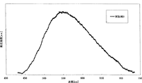
上記実施例1〜3および比較例1で得られた焼成物(蛍光体試料)を、それぞれ405nmの主波長を持つ光により励起し、その時の発光スペクトルを分光蛍光光度計(日立F4500)で測定した。実施例1、2及び比較例1の発光スペクトルを図3に、実施例3の発光スペクトルを図5示す。 The fired products (phosphor samples) obtained in Examples 1 to 3 and Comparative Example 1 were each excited with light having a dominant wavelength of 405 nm, and the emission spectrum at that time was measured with a spectrofluorometer (Hitachi F4500). did. The emission spectra of Examples 1 and 2 and Comparative Example 1 are shown in FIG. 3, and the emission spectrum of Example 3 is shown in FIG.
図3の発光スペクトルからわかるように、実施例1、2の蛍光体はそれぞれ発光ピークが455nm、475nm前後にあり、比較例1のβ‐SiAlON蛍光体と異なる発光を示した。なお発光ピークが600nm前後にあるユウロピウム付活Ca‐α‐SiAlON蛍光体(特開2001-214162号公報記載)の発光スペクトルとも異なることが示された。 As can be seen from the emission spectrum of FIG. 3, the phosphors of Examples 1 and 2 had emission peaks of around 455 nm and 475 nm, respectively, and emitted light different from the β-SiAlON phosphor of Comparative Example 1. It was shown that the emission spectrum of the europium-activated Ca-α-SiAlON phosphor (described in JP-A-2001-214162) having an emission peak around 600 nm is also different.
実施例1、2および比較例1の蛍光体の励起スペクトルを図4に示す。この励起スペクトルから、本発明の蛍光体が近紫外線領域(300〜420nm)により励起することがわかる。同時に、既存、蛍光体であるβ‐SiAlON蛍光体(比較例1)と異なる蛍光体であることもわかる。 The excitation spectra of the phosphors of Examples 1 and 2 and Comparative Example 1 are shown in FIG. From this excitation spectrum, it can be seen that the phosphor of the present invention is excited in the near ultraviolet region (300 to 420 nm). At the same time, it can be seen that the phosphor is different from the existing β-SiAlON phosphor (Comparative Example 1).
Al含有量の異なる実施例1(式(1)のx≒0.3)および実施例2(式(1)のx≒0.06)の結果からわかるように、アルミニウムの添加量が異なるO‐SiAlON蛍光体であっても蛍光特性が発現した。また図5に示すように、アルミニウムを含まないSinoite蛍光体(実施例3)であっても近紫外の励起により蛍光特性を発現した。実施例1〜3の発光スペクトルの比較からわかるように、アルミニウムの添加量が少ないほうが発光スペクトルはブロードな特性を示した。また添加量が少ないほうが発光ピーク波長は長波長となった。これによりアルミニウムの添加量を変えることにより蛍光体の特性を制御しうることが示された。 As can be seen from the results of Example 1 (x≈0.3 in formula (1)) and Example 2 (x≈0.06 in formula (1)) with different Al contents, the amount of aluminum added is different. -Fluorescence characteristics were expressed even with SiAlON phosphor. Further, as shown in FIG. 5, even the Sinoite phosphor not containing aluminum (Example 3) exhibited fluorescence characteristics by near-ultraviolet excitation. As can be seen from the comparison of the emission spectra of Examples 1 to 3, the emission spectrum showed broader characteristics as the amount of aluminum added was smaller. The emission peak wavelength became longer as the amount added was smaller. Thus, it was shown that the characteristics of the phosphor can be controlled by changing the amount of aluminum added.
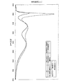
さらに実施例1および比較例1の蛍光体試料のX線回折パターンおよび既知物質であるCa‐α‐SiAlON蛍光体のX線回折パターンを図6に示す。これらX線回折パターンからも本発明のO‐SiAlON蛍光体が、従来のSiAlON蛍光体とは異なる結晶構造をとる新規蛍光体であることが確認できた。 Furthermore, the X-ray diffraction pattern of the phosphor sample of Example 1 and Comparative Example 1 and the X-ray diffraction pattern of the Ca-α-SiAlON phosphor which is a known substance are shown in FIG. From these X-ray diffraction patterns, it was confirmed that the O-SiAlON phosphor of the present invention was a new phosphor having a crystal structure different from that of the conventional SiAlON phosphor.
<実施例4、5>
次に、実施例1と同一組成のO-SiA10Nにおいて、付活剤である希土類元素等の濃度を異ならせて、蛍光体を製造した。
<Examples 4 and 5>
Next, in O-SiA10N having the same composition as in Example 1, phosphors were produced by changing the concentrations of rare earth elements as activators.
下記の原料化合物を、均一に乾式混合した。これを窒化ホウ素るつぼ(電気化学工業製)に投入し、多目的高温炉(富士電波工業製)内にいれた。炉内を10Paまで真空引きした後、0.92MPaの窒素で炉内を満たし、800℃で1時間維持した後1900℃で6時間維持して焼成を行った。このとき昇温速度を1425℃/hとし、冷却時は炉内にて放冷した。得られた焼成物の体色は灰色をしていた。焼成物をアルミナ乳鉢で解砕した後、篩別を行った。 The following raw material compounds were uniformly dry-mixed. This was put into a boron nitride crucible (manufactured by Denki Kagaku Kogyo) and placed in a multipurpose high temperature furnace (manufactured by Fuji Denpa Kogyo). The furnace was evacuated to 10 Pa, filled with 0.92 MPa of nitrogen, maintained at 800 ° C. for 1 hour, and then maintained at 1900 ° C. for 6 hours for firing. At this time, the temperature raising rate was set to 1425 ° C./h, and the system was allowed to cool in the furnace during cooling. The body color of the obtained fired product was gray. The fired product was crushed in an alumina mortar and then sieved.
実施例4の蛍光体の原料
Si3N4(宇部興産製) 0.960 mol
AlN(高純度化学製) 0.826 mol
Eu203(フルウチ化学製) O.115 mol
Si02(フルウチ化学製) 4.534 mol
Raw material for the phosphor of Example 4
Si 3 N 4 (Ube Industries) 0.960 mol
AlN (High purity chemical) 0.826 mol
Eu 2 0 3 (Furuuchi Chemical) O.115 mol
Si0 2 (Furuuchi Chemical) 4.534 mol
実施例5の蛍光体の原料
Si3N4(宇部興産製) 0.960 mo1
AlN(高純度化学製) 0.826 mo1
Eu203(フルウチ化学製) 0.005 mo1
Si02(フルウチ化学製) 4.534 mo1
Raw material for phosphor of Example 5
Si 3 N 4 (Ube Industries) 0.960 mo1
AlN (High purity chemical) 0.826 mo1
Eu 2 0 3 (Furuuchi Chemical) 0.005 mo1
Si0 2 (Furuuchi Chemical) 4.534 mo1
上記実施例4、5の蛍光体の発光スペクトルを実施例1の蛍光体の発光スペクトルとともに図7に示す。実施例4、5の蛍光体は、実施例1と同一組成のO-SiA10Nであり、付活剤であるユウロピウムの添加量を実施例1が0.2mo1%であるのに対し、それぞれ1mol%、0.05mo1%としたものである。図7の結果からわかるように、本発明のO‐SiAlON蛍光体は、付活剤濃度を変えることで発光波長を任意に変えることができる。 The emission spectra of the phosphors of Examples 4 and 5 are shown in FIG. 7 together with the emission spectrum of the phosphor of Example 1. The phosphors of Examples 4 and 5 are O-SiA10N having the same composition as that of Example 1. The amount of europium as an activator was 1 mol%, whereas Example 1 was 0.2 mol%. 0.05mo1%. As can be seen from the results of FIG. 7, the emission wavelength of the O-SiAlON phosphor of the present invention can be arbitrarily changed by changing the activator concentration.
次に、実施例2と同一組成のO-SiA10Nにおいて、付活剤である希土類元素等の種類を変えて、実施例6〜9の蛍光体を製造した。 Next, in O-SiA10N having the same composition as that in Example 2, phosphors of Examples 6 to 9 were manufactured by changing the kind of rare earth element as an activator.
<実施例6>
下記の原料化合物を、均一に乾式混合した。これを窒化ホウ素るつぼ(電気化学工業製)に投入し、多目的高温炉(富士電波工業製)内にいれた。炉内を10Paまで真空引きした後、0.92MPaの窒素で炉内を満たし、1800℃で6時間維持して焼成を行った。このとき昇温速度を1425℃/hとし、冷却時は炉内にて放冷した。得られた焼成物の体色は白色をしていた。焼成物をアルミナ乳鉢で解砕した後、篩別を行った。
Si3N4(宇部興産製) 0.451 mo1
AlN(高純度化学製) O.088 mo1
Eu203(フルウチ化学製) 0.011 mo1
Si02(フルウチ化学製) 1.354 mo1
MnCO3(高純度化学製) O.076 mo1
<Example 6>
The following raw material compounds were uniformly dry-mixed. This was put into a boron nitride crucible (manufactured by Denki Kagaku Kogyo) and placed in a multipurpose high temperature furnace (manufactured by Fuji Denpa Kogyo). After evacuating the furnace to 10 Pa, the furnace was filled with 0.92 MPa of nitrogen and maintained at 1800 ° C. for 6 hours for firing. At this time, the temperature raising rate was set to 1425 ° C./h, and the system was allowed to cool in the furnace during cooling. The body color of the obtained fired product was white. The fired product was crushed in an alumina mortar and then sieved.
Si 3 N 4 (Ube Industries) 0.451 mo1
AlN (High purity chemical) O.088 mo1
Eu 2 0 3 (Furuuchi Chemical) 0.011 mo1
Si0 2 (Furuuchi Chemical) 1.354 mo1
MnCO 3 (High purity chemical) O.076 mo1
<実施例7>
下記の原料化合物を、均一に乾式混合した。これを窒化ホウ素るつぼ(電気化学工業製)に投入し、多目的高温炉(富士電波工業製)内にいれた。炉内を10Paまで真空引きした後、0.92MPaの窒素で炉内を満たし、1900℃で8時間維持して焼成を行った。このとき昇温速度を1425℃/hとし、冷却時は炉内にて放冷した。得られた焼成物の体色は灰色をしていた。焼成物をアルミナ乳鉢で解砕した後、篩別を行った。
Si3N4(宇部興産製) 0.451 mo1
CeO2(高純度化学製) O.005 mo1
AlN(高純度化学製) O.088 mo1
Si02(高純度化学製) 1.354 mo1
<Example 7>
The following raw material compounds were uniformly dry-mixed. This was put into a boron nitride crucible (manufactured by Denki Kagaku Kogyo) and placed in a multipurpose high temperature furnace (manufactured by Fuji Denpa Kogyo). The furnace was evacuated to 10 Pa, filled with 0.92 MPa of nitrogen, and maintained at 1900 ° C. for 8 hours for firing. At this time, the temperature raising rate was set to 1425 ° C./h, and the system was allowed to cool in the furnace during cooling. The body color of the obtained fired product was gray. The fired product was crushed in an alumina mortar and then sieved.
Si 3 N 4 (Ube Industries) 0.451 mo1
CeO 2 (High purity chemical) O.005 mo1
AlN (High purity chemical) O.088 mo1
Si0 2 (High purity chemical) 1.354 mo1
<実施例8>
下記の原料化合物を、均一に乾式混合した。これを窒化ホウ素るつぼ(電気化学工業製)に投入し、多目的高温炉(富士電波工業製)内にいれた。炉内を10Paまで真空引きした後、0.92MPaの窒素で炉内を満たし、1800℃で6時間維持して焼成を行った。このとき昇温速度を1425℃/hとし、冷却時は炉内にて放冷した。得られた焼成物の体色は白色をしていた。焼成物をアルミナ乳鉢で解砕した後、篩別を行った。
Si3N4(宇部興産製) 0.451 mo1
Tb4O7(高純度化学製) O.006 mo1
AlN(高純度化学製) O.088 mo1
Si02(高純度化学製) 1.354 mo1
<Example 8>
The following raw material compounds were uniformly dry-mixed. This was put into a boron nitride crucible (manufactured by Denki Kagaku Kogyo) and placed in a multipurpose high temperature furnace (manufactured by Fuji Denpa Kogyo). After evacuating the furnace to 10 Pa, the furnace was filled with 0.92 MPa of nitrogen and maintained at 1800 ° C. for 6 hours for firing. At this time, the temperature raising rate was set to 1425 ° C./h, and the system was allowed to cool in the furnace during cooling. The body color of the obtained fired product was white. The fired product was crushed in an alumina mortar and then sieved.
Si 3 N 4 (Ube Industries) 0.451 mo1
Tb 4 O 7 (High purity chemical) O.006 mo1
AlN (High purity chemical) O.088 mo1
Si0 2 (High purity chemical) 1.354 mo1
<実施例9>
下記の原料化合物を、均一に乾式混合した。これを窒化ホウ素るつぼ(電気化学工業製)に投入し、多目的高温炉(富士電波工業製)内にいれた。炉内を10Paまで真空引きした後、0.92MPaの窒素で炉内を満たし、1800℃で6時間維持して焼成を行った。このとき昇温速度を1425℃/hとし、冷却時は炉内にて放冷した。得られた焼成物の体色は赤褐色をしていた。焼成物をアルミナ乳鉢で解砕した後、篩別を行った。
Si3N4(宇部興産製) 0.451 mo1
Sm2O3(高純度化学製) O.011 mo1
AlN(高純度化学製) O.088 mo1
Si02(高純度化学製) 1.354 mo1
<Example 9>
The following raw material compounds were uniformly dry-mixed. This was put into a boron nitride crucible (manufactured by Denki Kagaku Kogyo) and placed in a multipurpose high temperature furnace (manufactured by Fuji Denpa Kogyo). After evacuating the furnace to 10 Pa, the furnace was filled with 0.92 MPa of nitrogen and maintained at 1800 ° C. for 6 hours for firing. At this time, the temperature raising rate was set to 1425 ° C./h, and the system was allowed to cool in the furnace during cooling. The body color of the obtained fired product was reddish brown. The fired product was crushed in an alumina mortar and then sieved.
Si 3 N 4 (Ube Industries) 0.451 mo1
Sm 2 O 3 (High purity chemical) O.011 mo1
AlN (High purity chemical) O.088 mo1
Si0 2 (High purity chemical) 1.354 mo1
実施例6〜9の蛍光体の発光スペクトルを図8に示す。図8の結果からわかるように、本発明のO‐SiAlON蛍光体は、付活剤の種類を変えることで種々の発光を得ることが可能になる。 The emission spectra of the phosphors of Examples 6 to 9 are shown in FIG. As can be seen from the results of FIG. 8, the O-SiAlON phosphor of the present invention can obtain various luminescence by changing the type of activator.
<実施例10>
以下の手順で図1に示すような発光装置を作成した。
まず、基体7として、Agメッキされた引き出し電極6が高反射率を有したナイロン系樹脂により凹部8(壁となる端面角度約52°)と一体成型されたものを用意した。半導体発光素子1として、n型SiC基板上に形成されたInGaN系化合物半導体(発光波長ピーク395nm)を用意した。半導体発光素子1は、n型基板に形成されたカソード電極と対応する引き出し電極6にAgペーストにて電気的接合を得ると共に基体7に固定した。他方、InGaN系化合物半導体に形成されたアノード電極と対応する引き出し電極とはAuワイヤーにて電気的接合を確保した。波長変換材3として、実施例1のO‐SiAlON蛍光体と、黄色蛍光体であるオルト珪酸塩系蛍光体を適宜混合したものを用いた。この混合蛍光体をシリコーン樹脂に20wt%混合させたものを凹部8の開口部端まで充填し、150℃で2時間、樹脂硬化し発光素子を作製した。そのときの色度座標は(0.30,0.34)であった。
<Example 10>
A light emitting device as shown in FIG. 1 was prepared by the following procedure.
First, as the
<比較例2>
O‐SiAlON蛍光体を従来のBAM蛍光体(化成オプトニクス製)に変更し、色度座標が同じになるように調合した波長変換材料を用いて、実施例10と同様に発光装置を作製した。
<Comparative example 2>
The O-SiAlON phosphor was changed to a conventional BAM phosphor (manufactured by Kasei Optonics), and a light-emitting device was fabricated in the same manner as in Example 10 using a wavelength conversion material prepared so that the chromaticity coordinates were the same. .
実施例10および比較例2の発光装置の発光スペクトルと平均演色係数(Ra)を図9に示す。実施例10および比較例2の平均演色係数(Ra)は、それぞれ80、73であり、本発明のO‐SiAlON蛍光体を用いることにより演色性に優れた白色LED素子が得られることが確認された。 The emission spectra and average color rendering coefficient (Ra) of the light emitting devices of Example 10 and Comparative Example 2 are shown in FIG. The average color rendering coefficients (Ra) of Example 10 and Comparative Example 2 are 80 and 73, respectively, and it was confirmed that white LED elements having excellent color rendering properties can be obtained by using the O-SiAlON phosphor of the present invention. It was.
本発明によれば、従来のBAM蛍光体に比べ発光効率に優れた蛍光体が提供される。この蛍光体を用いることにより、演色性に優れた白色LED素子を作成することができる。本発明の蛍光体は、一般照明用光源、ストロボ用光源その他、近紫外発光蛍光体が用いられる全ての分野に適用することができる。 According to the present invention, a phosphor excellent in luminous efficiency as compared with a conventional BAM phosphor is provided. By using this phosphor, a white LED element excellent in color rendering can be produced. The phosphor of the present invention can be applied to all fields in which near-ultraviolet phosphors are used, such as general illumination light sources, strobe light sources, and the like.
1・・・発光素子、2・・・導線、3・・・波長変換材、4・・・封止部、6・・・引き出し電極、7・・・基体、8・・・凹部。
DESCRIPTION OF
Claims (9)
A2-xBxO1+xN2-x:RE (1)
(式中、AはSi、Ge、Cから選択される1種または2種以上の元素、BはA1、Ga、B、Inから選択される1種または2種以上の元素、REはCe、Pr、Nd、Sm、Eu、Gd、Tb、Dy、Ho、Er、Tm、Yb、LuおよびMnから選ばれる1種または2種以上の元素を表す。xは0≦x<0.3を満たす数値を表す。) A phosphor that is represented by the general formula (1) and emits light by near-ultraviolet irradiation.
A 2-x B x O 1 + x N 2-x : RE (1)
(Wherein A is one or more elements selected from Si, Ge and C, B is one or more elements selected from A1, Ga, B and In, RE is Ce, Represents one or more elements selected from Pr, Nd, Sm, Eu, Gd, Tb, Dy, Ho, Er, Tm, Yb, Lu, and Mn, where x satisfies 0 ≦ x <0.3. (Represents a numerical value.)
前記波長変換材料として、請求項1ないし4いずれか1項記載の蛍光体を含むことを特徴とする発光装置。 A semiconductor light emitting element, an electrode connected to the light emitting element, at least one wavelength conversion material that absorbs light emitted from the light emitting element and emits light having a wavelength different from that of light emitted from the light emitting element; In a light emitting device having a sealing material for sealing the light emitting element,
A light emitting device comprising the phosphor according to claim 1 as the wavelength conversion material.
前記発光素子は、発光ピーク波長が300〜420nmの範囲であることを特徴とする発光装置。 The light-emitting device according to claim 7,
The light emitting device has a light emission peak wavelength in a range of 300 to 420 nm.
前記封止材は、エポキシ樹脂、シリコーン樹脂、エポキシ基を有するポリジメチルシロキサン誘導体、オキセタン樹脂、アクリル樹脂、シクロオレフィン樹脂から選ばれる1種または2種以上の樹脂からなることを特徴とする発光装置。
The light-emitting device according to claim 7 or 8,
The said sealing material consists of 1 type, or 2 or more types of resin chosen from an epoxy resin, a silicone resin, the polydimethylsiloxane derivative which has an epoxy group, an oxetane resin, an acrylic resin, and a cycloolefin resin, The light-emitting device characterized by the above-mentioned .
Priority Applications (1)
| Application Number | Priority Date | Filing Date | Title |
|---|---|---|---|
| JP2006186908A JP4863794B2 (en) | 2006-07-06 | 2006-07-06 | Wavelength converting material, method for producing the same, and light emitting device using the same |
Applications Claiming Priority (1)
| Application Number | Priority Date | Filing Date | Title |
|---|---|---|---|
| JP2006186908A JP4863794B2 (en) | 2006-07-06 | 2006-07-06 | Wavelength converting material, method for producing the same, and light emitting device using the same |
Publications (2)
| Publication Number | Publication Date |
|---|---|
| JP2008013674A JP2008013674A (en) | 2008-01-24 |
| JP4863794B2 true JP4863794B2 (en) | 2012-01-25 |
Family
ID=39071008
Family Applications (1)
| Application Number | Title | Priority Date | Filing Date |
|---|---|---|---|
| JP2006186908A Expired - Fee Related JP4863794B2 (en) | 2006-07-06 | 2006-07-06 | Wavelength converting material, method for producing the same, and light emitting device using the same |
Country Status (1)
| Country | Link |
|---|---|
| JP (1) | JP4863794B2 (en) |
Families Citing this family (3)
| Publication number | Priority date | Publication date | Assignee | Title |
|---|---|---|---|---|
| JP5586006B2 (en) | 2007-03-28 | 2014-09-10 | 国立大学法人広島大学 | M—C—N—O phosphor |
| CN104099092A (en) * | 2013-04-09 | 2014-10-15 | 海洋王照明科技股份有限公司 | Dysprosium-doped alkali fluoborosilicate glass up-conversion luminescent material, and preparation method and application thereof |
| NL2021109B1 (en) * | 2018-06-12 | 2019-12-17 | Physee Group B V | Inorganic luminescent materials for solar radiation conversion devices |
-
2006
- 2006-07-06 JP JP2006186908A patent/JP4863794B2/en not_active Expired - Fee Related
Also Published As
| Publication number | Publication date |
|---|---|
| JP2008013674A (en) | 2008-01-24 |
Similar Documents
| Publication | Publication Date | Title |
|---|---|---|
| JP5190475B2 (en) | Phosphor and light emitting device using the same | |
| US7811472B2 (en) | Phosphor composition and method for producing the same, and light-emitting device using the same | |
| JP4892193B2 (en) | Phosphor mixture and light emitting device | |
| US8709838B2 (en) | Method for preparing a β-SiAlON phosphor | |
| JP5446066B2 (en) | Nitride phosphor and light emitting device using the same | |
| KR101172143B1 (en) | OXYNITRIDE-BASED PHOSPHORS COMPOSING OF SiON ELEMENT FOR WHITE LEDs, MANUFACTURING METHOD THEREOF AND LEDs USING THE SAME | |
| JP4892861B2 (en) | Nitride phosphor and light emitting device using the same | |
| KR20070061865A (en) | Phospher, process for producing the same and luminescence apparatus | |
| US9657222B2 (en) | Silicate phosphors | |
| JP2004186278A (en) | Light emitting device and method therefor | |
| JP2008163078A (en) | Phosphor and light-emitting device using the same | |
| WO2007004492A1 (en) | Fluorophor and method for production thereof and illuminator | |
| JP5412710B2 (en) | Nitride-based phosphor or oxynitride-based phosphor | |
| JP2010268004A (en) | Red phosphor and light-emitting device using the same | |
| JP2010270196A (en) | Phosphor, method for manufacturing phosphor, phosphor-containing composition, light-emitting device, lighting apparatus, image display, and fluorescent paint | |
| JP5100059B2 (en) | Phosphor, method for producing the same, and light emitting device using the same | |
| US20120062103A1 (en) | Red light-emitting fluorescent substance and light-emitting device employing the same | |
| EP2448020A1 (en) | Light emitting module | |
| CN107636113B (en) | Phosphor, method for producing same, and LED lamp | |
| JP2009079069A (en) | Carbonitride-based fluorophor and light-emitting device using the same and method for producing carbonitride-based fluorophor | |
| JP4863794B2 (en) | Wavelength converting material, method for producing the same, and light emitting device using the same | |
| KR101176212B1 (en) | Alkali-earth Phosporus Nitride system phosphor, manufacturing method thereof and light emitting devices using the same | |
| JP4948015B2 (en) | Aluminate blue phosphor and light emitting device using the same | |
| JP5194395B2 (en) | Oxynitride phosphor and light-emitting device using the same | |
| JP2009138070A (en) | Phosphor, method for producing the same, and light-emitting device using phosphor |
Legal Events
| Date | Code | Title | Description |
|---|---|---|---|
| A621 | Written request for application examination |
Free format text: JAPANESE INTERMEDIATE CODE: A621 Effective date: 20090422 |
|
| A977 | Report on retrieval |
Free format text: JAPANESE INTERMEDIATE CODE: A971007 Effective date: 20111031 |
|
| TRDD | Decision of grant or rejection written | ||
| A01 | Written decision to grant a patent or to grant a registration (utility model) |
Free format text: JAPANESE INTERMEDIATE CODE: A01 Effective date: 20111108 |
|
| A01 | Written decision to grant a patent or to grant a registration (utility model) |
Free format text: JAPANESE INTERMEDIATE CODE: A01 |
|
| A61 | First payment of annual fees (during grant procedure) |
Free format text: JAPANESE INTERMEDIATE CODE: A61 Effective date: 20111108 |
|
| FPAY | Renewal fee payment (event date is renewal date of database) |
Free format text: PAYMENT UNTIL: 20141118 Year of fee payment: 3 |
|
| R150 | Certificate of patent or registration of utility model |
Ref document number: 4863794 Country of ref document: JP Free format text: JAPANESE INTERMEDIATE CODE: R150 Free format text: JAPANESE INTERMEDIATE CODE: R150 |
|
| R250 | Receipt of annual fees |
Free format text: JAPANESE INTERMEDIATE CODE: R250 |
|
| R250 | Receipt of annual fees |
Free format text: JAPANESE INTERMEDIATE CODE: R250 |
|
| R250 | Receipt of annual fees |
Free format text: JAPANESE INTERMEDIATE CODE: R250 |
|
| R250 | Receipt of annual fees |
Free format text: JAPANESE INTERMEDIATE CODE: R250 |
|
| R250 | Receipt of annual fees |
Free format text: JAPANESE INTERMEDIATE CODE: R250 |
|
| LAPS | Cancellation because of no payment of annual fees |