JP5206242B2 - Power storage device and method for manufacturing power storage device - Google Patents
Power storage device and method for manufacturing power storage device Download PDFInfo
- Publication number
- JP5206242B2 JP5206242B2 JP2008224163A JP2008224163A JP5206242B2 JP 5206242 B2 JP5206242 B2 JP 5206242B2 JP 2008224163 A JP2008224163 A JP 2008224163A JP 2008224163 A JP2008224163 A JP 2008224163A JP 5206242 B2 JP5206242 B2 JP 5206242B2
- Authority
- JP
- Japan
- Prior art keywords
- collector plate
- current collector
- contact surface
- predetermined axis
- contact
- Prior art date
- Legal status (The legal status is an assumption and is not a legal conclusion. Google has not performed a legal analysis and makes no representation as to the accuracy of the status listed.)
- Expired - Fee Related
Links
Images


Classifications
-
- Y—GENERAL TAGGING OF NEW TECHNOLOGICAL DEVELOPMENTS; GENERAL TAGGING OF CROSS-SECTIONAL TECHNOLOGIES SPANNING OVER SEVERAL SECTIONS OF THE IPC; TECHNICAL SUBJECTS COVERED BY FORMER USPC CROSS-REFERENCE ART COLLECTIONS [XRACs] AND DIGESTS
- Y02—TECHNOLOGIES OR APPLICATIONS FOR MITIGATION OR ADAPTATION AGAINST CLIMATE CHANGE
- Y02E—REDUCTION OF GREENHOUSE GAS [GHG] EMISSIONS, RELATED TO ENERGY GENERATION, TRANSMISSION OR DISTRIBUTION
- Y02E60/00—Enabling technologies; Technologies with a potential or indirect contribution to GHG emissions mitigation
- Y02E60/10—Energy storage using batteries
Description
本発明は、正極素子および負極素子がセパレータ(電解質層)を挟んで巻かれた構造を有する蓄電装置に関するものである。 The present invention relates to a power storage device having a structure in which a positive electrode element and a negative electrode element are wound with a separator (electrolyte layer) interposed therebetween.
二次電池は、充放電を行うための発電要素と、発電要素を収容するための電池ケースとを有している。ここで、発電要素は、正極素子、負極素子およびセパレータを有している。例えば、正極素子および負極素子の間にセパレータを配置したものを、芯部材に対して巻き付けることにより、発電要素を構成することができる(例えば、特許文献1−3参照)。 The secondary battery has a power generation element for charging and discharging and a battery case for housing the power generation element. Here, the power generation element has a positive electrode element, a negative electrode element, and a separator. For example, a power generation element can be configured by winding a core member with a separator disposed between a positive electrode element and a negative electrode element (see, for example, Patent Documents 1-3).
また、電池ケースには、発電要素に蓄えられた電力を取り出したり、発電要素に電力を蓄えたりするために用いられる電極端子(正極端子および負極端子)が設けられている。特許文献1に記載の二次電池では、正極端子が、電池ケースの一端面に固定されており、リード線を介して発電要素の正極素子と電気的および機械的に接続されている。また、負極端子は、電池ケースの他端面に固定されており、リード線を介して発電要素の負極素子と電気的および機械的に接続されている。
リード線を介して発電要素を電極端子に接続する構成では、リード線を用いる分だけ、二次電池のコストが高くなってしまう。また、電極端子や発電要素に対してリード線を接続するための領域を設けたり、二次電池内にリード線を配置するためのスペースを確保したりしなければならないため、二次電池が大型化してしまうことがある。 In the configuration in which the power generation element is connected to the electrode terminal via the lead wire, the cost of the secondary battery is increased by the amount of use of the lead wire. In addition, since a region for connecting the lead wire to the electrode terminal and the power generation element must be provided or a space for arranging the lead wire in the secondary battery must be secured, the secondary battery is large. It may become.
そこで、本発明の目的は、リード線を用いずに、小型化することができる蓄電装置を提供することにある。 Accordingly, an object of the present invention is to provide a power storage device that can be reduced in size without using a lead wire.
本願第1の発明である蓄電装置は、所定軸の周りで巻かれた電極素子と、電極素子と電気的に接続される電極端子と、を有している。そして、電極端子は、集電板のうち所定軸の方向における端部であって、電極層が形成されていない端部と接触し、所定軸の周りに延びる接触面を有している。また、接触面は、所定軸から離れる方向を向くとともに、所定軸に沿って集電板の端部から離れる方向において、所定軸から接触面までの距離が連続的又は段階的に増加している。 The power storage device according to the first invention of the present application includes an electrode element wound around a predetermined axis, and an electrode terminal electrically connected to the electrode element. The electrode terminal has a contact surface that is an end portion of the current collector plate in the direction of the predetermined axis and is in contact with an end portion on which the electrode layer is not formed and extends around the predetermined axis . Further, the contact surface faces a direction away from the predetermined axis, and the distance from the predetermined axis to the contact surface increases continuously or stepwise in a direction away from the end of the current collector plate along the predetermined axis . .
接触面としては、所定軸を中心とした円錐面に沿った形状に形成することができる。これにより、接触面に対して、集電板の端部を巻き付けやすくすることができる。 As a contact surface, it can form in the shape along the conical surface centering on the predetermined axis. Thereby, the edge part of a current collecting plate can be made easy to wind around a contact surface.
集電板のうち電極層の形成されていない領域を、接触面に沿って曲げた状態で接触面に接触させることができる。これにより、集電板および接触面における接触面積を確保することができる。 The area | region in which the electrode layer is not formed among current collector plates can be made to contact a contact surface in the state bent along the contact surface. Thereby, the contact area in a current collecting plate and a contact surface is securable.
集電板の端部は、接触面に溶接することができる。集電板および接触面を溶接することにより、電極端子および集電板の間における電気抵抗を低減させることができる。また、集電板の端部に、切り欠き部を形成することができる。これにより、集電板の端部を電極端子の接触面に巻き付ける際に、集電板の端部に対して過度の負荷がかかるのを抑制することができる。 The end of the current collector plate can be welded to the contact surface. By welding the current collector plate and the contact surface, it is possible to reduce the electrical resistance between the electrode terminal and the current collector plate. Moreover, a notch part can be formed in the edge part of a current collecting plate . Thus, it is possible to suppress the time of winding the end of the current collector plate to the contact surface of the electrode terminal, an excessive load to the end portion of the current collector plate from being applied.
なお、蓄電装置に設けられる正極端子および負極端子のうち少なくとも一方の端子を、本発明における電極端子とすることができる。 Note that at least one of the positive electrode terminal and the negative electrode terminal provided in the power storage device can be used as an electrode terminal in the present invention.
本願第2の発明は、所定軸の周りで巻かれた電極素子と、電極素子と電気的に接続される電極端子とを有する蓄電装置の製造方法である。電極素子は、集電板と、集電板における一部の領域に形成された電極層とを有する。電極端子は、集電板のうち所定軸の方向における端部であって、電極層が形成されていない端部と接触し、所定軸の周りに延びる接触面を有する。また、電極端子の接触面が、所定軸から離れる方向を向くとともに、所定軸に沿って集電板の端部から離れる方向において、所定軸から接触面までの距離が連続的又は段階的に増加している。ここで、電極素子を所定軸の周りで巻きながら、接触面に対して集電板の端部を接触させる。 Second aspect of the invention, Ru manufacturing method der power storage device having electrodes elements wrapped around a predetermined axis, and an electrode terminal connected to electrode elements electrically. The electrode element has a current collector plate and an electrode layer formed in a partial region of the current collector plate. The electrode terminal is in an end portion in the direction of the predetermined axis of the current collector plate, and has a contact surface that is in contact with an end portion where the electrode layer is not formed and extends around the predetermined axis. In addition, the contact surface of the electrode terminal faces away from the predetermined axis, and the distance from the predetermined axis to the contact surface increases continuously or stepwise in the direction away from the end of the current collector plate along the predetermined axis. Is doing. Here, while winding the electrode elements around the predetermined axis, Ru contacting the end of the current collector plate to the contact surface.
ここで、電極素子を巻きながら、集電板の端部を接触面に溶接することができる。具体的には、集電板のうち接触面との接触部分に対して、レーザ光を照射することにより溶接を行うことができる。これにより、集電板および電極端子の間における電気抵抗を低減させることができる。 Here, the end of the current collector plate can be welded to the contact surface while winding the electrode element. Specifically, welding can be performed by irradiating a portion of the current collector plate that contacts the contact surface with laser light. Thereby, the electrical resistance between a current collecting plate and an electrode terminal can be reduced.
また、集電板を接触面に接触させる前に、集電板の端部を接触面に沿った形状に曲げておくことができる。これにより、電極素子(集電板)を電極端子に対してスムーズに巻き付けることができる。
Further, it is possible before contacting the current collector plate to the contact surface, previously bent into a shape along the contact surface end of the current collector plate. Thereby, an electrode element (current collector plate) can be smoothly wound around an electrode terminal.
本願第1の発明では、リード線等を用いることなく、電極素子(集電板)を電極端子に接触させているため、蓄電装置を小型化することができる。しかも、本発明のように電極端子の接触面を構成することにより、電極素子を所定軸の周りで巻く際に、集電板の端部を電極端子に接触させやすくなる。 In the first invention of the present application, since the electrode element (current collector plate) is brought into contact with the electrode terminal without using a lead wire or the like, the power storage device can be reduced in size. In addition, by configuring the contact surface of the electrode terminal as in the present invention, the end of the current collector plate can be easily brought into contact with the electrode terminal when the electrode element is wound around the predetermined axis.
本願第2の発明によれば、電極端子の接触面に対して、電極素子(集電板)を容易に接触させることができる。言い換えれば、電極素子を所定軸の周りで巻く際に、電極端子の接触面に対して電極素子(集電板)を巻き付けやすくなる。これにより、蓄電装置を容易に製造することができる。
According to the second aspect of the present invention, the electrode element (current collector plate) can be easily brought into contact with the contact surface of the electrode terminal. In other words, when the electrode element is wound around the predetermined axis, the electrode element (current collector plate) can be easily wound around the contact surface of the electrode terminal. Thereby, an electrical storage apparatus can be manufactured easily.
以下、本発明の実施例について説明する。 Examples of the present invention will be described below.
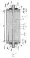
本発明の実施例1である二次電池(蓄電装置)の構造について、図1および図2を用いて説明する。ここで、図1は、二次電池の内部構造を示す断面図であり、図2は、図1の矢印Aで示す方向から見たときの二次電池の外観図である。なお、二次電池としては、例えば、ニッケル水素電池やリチウムイオン電池といったものが挙げられる。また、本実施例では、二次電池を用いた場合について説明するが、蓄電装置としての電気二重層キャパシタ(コンデンサ)についても本発明を適用することができる。
A structure of a secondary battery (power storage device) that is
本実施例の二次電池1は、例えば、車両の動力源として用いることができる。この車両としては、例えば、ハイブリッド自動車や電気自動車がある。ハイブリッド自動車とは、動力源としての二次電池に加えて、内燃機関や燃料電池といった他の動力源を備えた車両である。電気自動車とは、二次電池1の出力だけを用いて走行する車両である。本実施例の二次電池1を車両に搭載する場合には、車両の走行に必要なエネルギを取り出すために、複数の二次電池を用いる必要がある。具体的には、複数の二次電池を電気的に直列に接続することにより、車両の走行に必要な電力を確保する必要がある。
The
二次電池1は、巻かれた状態の発電要素10と、発電要素10を収容する電池ケース20とを有している。電池ケース20は、円筒状に形成された円筒部21と、円筒部21の両端に固定される平板部22,23とを有している。また、電池ケース20は、耐久性および耐食性に優れた材料で形成することが好ましく、この材料として、具体的には、アルミニウム等の金属を用いることができる。なお、電池ケース20を樹脂で形成することも可能である。
The
平板部22,23は、例えば、円筒部21に対して溶接によって固定することができる。また、平板部22,23には、後述する正極端子40および負極端子50を貫通させるための穴部22a,23aが形成されている。
The
発電要素10は、充放電が可能な要素であり、電極素子としての正極素子11および負極素子12と、セパレータ13とを有している。セパレータ13は、正極素子11および負極素子12の間に位置するように配置されている。すなわち、正極素子11、セパレータ13および負極素子12を、この順に積層することにより、発電要素10が構成される。ここで、セパレータ13には、例えば、真空状態での注液処理等により、電解液がしみ込んでいる。
The
正極素子11、負極素子12およびセパレータ13は、互いに重ねられた状態で、芯部材30に巻き付けられている。芯部材30の両端、言い換えれば、電池ケース20の両端面には、電極端子としての正極端子40および負極端子50が配置されている。
The
正極素子11は、図3Aに示すように、正極用の集電板11aと、集電板11aの両面に形成された活物質層(電極層)11bとを有している。図3Aでは、集電板11aの一方の面だけを示しているが、他方の面も同様の構成となっている。ここで、領域R1は、集電板11aのうち、活物質層11bが形成されていない領域であり、図1に示すように、正極端子40(接触面42b)と接触する領域である。また、領域R2は、集電板11aのうち、活物質層11bが形成されている領域である。
As shown in FIG. 3A, the
二次電池1として、リチウムイオン電池を用いる場合には、例えば、集電板11aをアルミニウムで形成することができる。また、活物質層11bは、正極に応じた活物質を有しており、必要に応じて結着剤や導電剤が含まれる。正極活物質としては、ニッケル水素電池の場合にはニッケル酸化物を用い、リチウムイオン電池の場合にはリチウム−遷移金属複合酸化物を用いることができる。
When a lithium ion battery is used as the
負極素子12は、図3Bに示すように、負極用の集電板12aと、集電板12aの両面に形成された活物質層(電極層)12bとを有している。図3Bでは、集電板12aの一方の面だけを示しているが、他方の面も同様の構成となっている。ここで、領域R2は、集電板12aのうち、活物質層12bが形成されている領域である。また、領域R3は、活物質層12bが形成されていない領域であり、図1に示すように、負極端子50(接触面52b)と接触する領域である。
As shown in FIG. 3B, the
二次電池1として、リチウムイオン電池を用いる場合には、例えば、集電板12aを銅で形成することができる。また、活物質層12bは、負極に応じた活物質を有しており、必要に応じて結着剤や導電剤が含まれる。負極活物質としては、ニッケル水素電池の場合にはMmNi(5−x−y−z)AlxMnyCoz(Mm:ミッシュメタル)等の水素吸蔵合金を用い、リチウムイオン電池の場合にはカーボンを用いることができる。
When a lithium ion battery is used as the
正極素子11および負極素子12における領域R2は、充放電に用いられる領域であり、芯部材30の長手方向に関して互いに重なるようになっている。ここで、セパレータ13は、領域R2上に位置していればよい。
The region R <b> 2 in the
なお、本実施例では、集電板11aの両面に正極用の活物質層11bを形成し、集電板12aの両面に負極用の活物質層12bを形成しているが、これに限るものではない。具体的には、集電板の一方の面に正極用の活物質層を形成するとともに、集電板の他方の面に負極用の活物質層を形成することができる。これは、いわゆるバイポーラ電極と呼ばれるものである。
In this embodiment, the positive electrode
正極端子40は、芯部材30に沿って延びる軸部41と、芯部材30の長手方向(図1の左右方向)と直交する方向に延びるフランジ部42とを有している。軸部41の外周面には、ナット70のネジ部と係合するネジ部が形成されている。また、軸部41および平板部22の穴部22aの間には、絶縁性を有する材料で形成されたシール部材60が配置されている。これにより、電池ケース20の内部を密閉状態とすることができるとともに、電池ケース20および正極端子40の間を絶縁状態とすることができる。ここで、シール部材60は、正極端子40(フランジ部42)およびワッシャ61によって挟まれている。また、ワッシャ61は、ナット70を軸部41に係合させることにより、固定される。
The
フランジ部42は、電池ケース20の平板部22と対向する平面42aと、発電要素10と電気的および機械的に接続される接触面42bとを有している。平面42aは、シール部材60と接触している。接触面42bは、発電要素10の正極素子11(集電板11a)と接触している。また、接触面42bは、芯部材30を中心とした円錐面で構成されている。より具体的には、接触面42bは、芯部材30を中心とした円錐面に沿った形状に形成されており、発電要素10(負極端子50)の側に向かって凸となる形状を有している。ここで、芯部材30の長手方向(図1の左右方向)における接触面42bおよび平面42aの間の距離は、芯部材30と接する側が最も長く、芯部材30から離れるにしたがって短くなっている。
The
負極端子50は、芯部材30に沿って延びる軸部51と、芯部材30の長手方向と直交する方向に延びるフランジ部52とを有している。軸部51の外周面には、ナット90のネジ部と係合するネジ部が形成されている。また、軸部51および平板部23の穴部23aの間には、絶縁性を有する材料で形成されたシール部材80が配置されている。これにより、電池ケース20の内部を密閉状態とすることができるとともに、電池ケース20および負極端子50の間を絶縁状態とすることができる。ここで、シール部材80は、負極端子50(フランジ部52)およびワッシャ81によって挟まれている。また、ワッシャ81は、ナット90を軸部51に係合させることにより、固定される。
The
フランジ部52は、電池ケース20の平板部23と対向する平面52aと、発電要素10と電気的および機械的に接続される接触面52bとを有している。平面52aは、シール部材80と接触している。接触面52bは、発電要素10の負極素子12(集電板12a)と接触している。また、接触面52bは、芯部材30を中心とした円錐面で構成されている。より具体的には、接触面52bは、芯部材30を中心とした円錐面に沿った形状に形成されており、発電要素10(正極端子40)の側に向かって凸となる形状を有している。ここで、芯部材30の長手方向(図1の左右方向)における接触面52bおよび平面52aの間の距離は、芯部材30と接する側が最も長く、芯部材30から離れるにしたがって短くなっている。
The
ここで、電池ケース20が金属で形成されている場合には、円筒部21の内壁面は絶縁材料で形成された層が設けられている。すなわち、絶縁層を用いることにより、正極端子40のフランジ部42や負極端子50のフランジ部52が、円筒部21の内壁面に直接、接触するのを阻止している。
Here, when the
次に、本実施例の二次電池1を製造する工程について、図4を用いて説明する。ここで、図4は、発電要素10を芯部材30に巻き付ける工程を示す図である。
Next, the process of manufacturing the
発電要素10を芯部材30に巻き付ける前に、まず、正極素子11、負極素子12およびセパレータ13を用意しておく。そして、正極素子11、セパレータ13および負極素子12を、この順に積層して構成された発電要素10を、芯部材30に巻き付けていく。具体的には、芯部材30に固定された正極端子40および負極端子50を矢印Xで示す方向に回転させることにより、発電要素10が芯部材30に対して矢印Yで示す方向に移動して、芯部材30に巻き付いていく。
Before winding the
このとき、集電板11aの領域R1は、フランジ部42の接触面42bに接触し、集電板12aの領域R3は、フランジ部52の接触面52bに接触する。ここで、本実施例では、図1に示すように、集電板11a,12aをフランジ部42,52の先端側まで巻き付けるようにしている。このため、芯部材30の外周面に沿って、集電板11a,12aを巻き付けると、図5および図6に示すように、集電板11aにおける領域R1の一部がフランジ部42の接触面42bに沿うように変形する。
At this time, the region R1 of the
そして、図1に示すように、領域R2の端部と各接触面42b,52bとの間の距離(図1の左右方向の距離)は、芯部材30から離れるにしたがって、長くなっている。ここで、領域R1,R3のうち、芯部材30の近くに位置する各領域R1,R3は、各接触面42b,52bとの接触面積が最も大きくなっている。そして、芯部材30から離れるにつれて、各領域R1,R3における各接触面42b,52bとの接触面積が小さくなる。
As shown in FIG. 1, the distance between the end of the region R <b> 2 and the contact surfaces 42 b and 52 b (the distance in the left-right direction in FIG. 1) becomes longer as the distance from the
なお、図5および図6では、領域R1の一部が接触面42bに沿って曲げられた状態を示しているが、領域R1の全体が接触面42bに沿って曲げられていてもよい。特に、芯部材30に近い側では、領域R1の全体が接触面42bに沿って曲げられることもある。また、図5および図6では、集電板11aおよびフランジ部42の接触状態を示しているが、集電板12aおよびフランジ部52の接触状態も同様である。
5 and 6 show a state in which a part of the region R1 is bent along the
そして、集電板11aのうち接触面42bとの接触部分に対して、レーザ照射装置100からのレーザ光を照射することにより、集電板11aを接触面42bに溶接することができる。すなわち、芯部材30に対して発電要素10を巻きながら、集電板11aおよび接触面42bの接触部分に対してレーザ光を照射することができる。なお、集電板12aおよびフランジ部52についても、同様の方法で溶接することができる。ここで、レーザ照射装置100は、例えば、レーザ光を生成する発振器と、発振器で生成されたレーザ光を集光させた状態で対象物(集電板11aおよび接触面42b)に向かわせる光学系とで構成することができる。
And the
本実施例では、集電板11aの一部(端部)を曲げた状態で接触面42bに接触させている。すなわち、集電板11aおよび接触面42bの接触面積を確保するようにしている。これにより、レーザ光を用いて、集電板11aおよび接触面42bを容易に溶接することができる。
In the present embodiment, a part (end) of the
ここで、図7は、本実施例の比較例としての構成を示す概略図であり、図6に対応した図である。図7において、本実施例で説明した部材と同一の機能を有する部材については、同一符号を用いている。 Here, FIG. 7 is a schematic diagram showing a configuration as a comparative example of the present embodiment, and corresponds to FIG. In FIG. 7, the same reference numerals are used for members having the same functions as those described in this embodiment.
図7に示す構成では、フランジ部42のうち、集電板11aと接触する面42cを、芯部材30の長手方向と直交する平面で構成している。この構成では、集電板11aの端部だけを平面42cに接触させるようにしているため、集電板11aおよび平面42cは点接触となる。この場合には、集電板11aおよび平面42cの接触部分に対して、レーザ照射装置100のレーザ光を照射し難く、集電板11aおよび平面42cを溶接し難いことがある。
In the configuration shown in FIG. 7, the
なお、図7に示す構成でも、本実施例のように、集電板11aの一部を曲げた状態で平面42cに接触させれば、レーザ光を照射し易くすることができる。ただし、この場合には、芯部材30に対して、集電板11aを巻きにくくなってしまうことがある。
In the configuration shown in FIG. 7 as well, it is possible to easily irradiate the laser beam by contacting the
本実施例において、接触面42bの傾斜角度(テーパ角度)θ(図6参照)は、90[deg]よりも小さく、0[deg]よりも大きければよい。ここで、傾斜角度θを90[deg]に近づければ、芯部材30の長手方向において、二次電池1を小型化することができる。また、傾斜角度θを0[deg]に近づければ、集電板11aの端部(領域R1)を接触面42bに沿って変形させやすくしたり、集電板11aおよび接触面42bの接触面積を増やしたりすることができる。上述した観点に基づいて、接触面42bの傾斜角度θは、適宜設定することができる。接触面52bについても同様である。
In the present embodiment, the inclination angle (taper angle) θ (see FIG. 6) of the
ここで、本実施例では、接触面42b,52bの傾斜角度θを互いに等しくしているが、これに限るものではない。すなわち、接触面42b,52bの傾斜角度θを、互いに異なる値とすることもできる。 Here, in the present embodiment, the inclination angles θ of the contact surfaces 42b and 52b are equal to each other, but the present invention is not limited to this. That is, the inclination angles θ of the contact surfaces 42b and 52b can be different from each other.
一方、集電板11aを接触面42bに溶接する場合において、レーザ照射装置100によるレーザ光の照射方法は適宜設定することができる。例えば、集電板11aおよび接触面42bの接触部分に対して常にレーザ光を照射させておくこともできるし、レーザ光を間欠的に照射させることもできる。常にレーザ光を照射させておけば、集電板11aの領域R1のすべてを接触面42bに溶接することができる。このように、集電板11aおよび接触面42bの溶接部分を増やすほど、集電板11aおよび接触面42bの間における電気抵抗を小さくすることができる。そして、電気抵抗を小さくすることにより、二次電池1の出力性能を向上させることができる。
On the other hand, when the
また、レーザ光を間欠的に照射する場合において、レーザ光を照射するタイミングや、レーザ光を照射し続ける時間は、適宜設定することができる。具体的には、集電板11aおよび接触面42bの溶接部分を予め決めておけば、この溶接部分に対してレーザ光を照射するようにすればよい。この場合には、芯部材30の回転速度(発電要素10を巻く速度)や、レーザ光の照射タイミングおよび照射時間を制御することになる。
Further, in the case of intermittently irradiating laser light, the timing of irradiating the laser light and the time for continuously irradiating the laser light can be set as appropriate. Specifically, if the welded portions of the
本実施例によれば、発電要素10を芯部材30に巻き付けながら、集電板11a,12aおよび接触面42b,52bの接触部分にレーザ光を照射することにより、発電要素10を正極端子40および負極端子50に容易に接続することができる。また、特許文献1のように、リード線を用いて、発電要素10および電極端子40,50を接続する必要もない。そして、リード線を用いない分だけ、二次電池1のコストを低減したり、二次電池1を小型化したりすることができる。
According to the present embodiment, while the
本実施例のように、集電板11aの領域R1を接触面42bの斜面に沿って曲げると、領域R1の一部に対して過度の負荷(曲げ応力)が作用することがある。そこで、図8に示すように、集電板11aの領域R1に対して切り欠き部11a1を予め形成しておけば、集電板11aの領域R1を接触面42bに沿って巻いても、領域R1に対して過度の負荷がかかるのを抑制することができる。ここで、切り欠き部11a1の形状や、切り欠き部11a1を形成する位置や数は、適宜設定することができる。すなわち、集電板11aの領域R1に過度の曲げ応力がかからないように、切り欠き部11a1の位置や数を決定すればよい。集電板12aについても、集電板11aと同様に、切り欠き部を形成することができる。
If the region R1 of the
また、集電板11aを接触面42bに沿って巻き付けやすいように、集電板11aの領域R1を予め曲げておくこともできる。具体的には、図9に示すように、ガイド部材101を用いることにより、集電板11aの領域R1や集電板12aの領域R3を、芯部材30に巻き付ける前に所定方向に曲げておくことができる。ここで、所定方向とは、接触面42b,52bに沿った方向である。ガイド部材101は、集電板11aの領域R1に曲率を持たせるための曲げ部101aと、集電板12aの領域R3に曲率を持たせるための曲げ部101bとを有している。
Further, the region R1 of the
ガイド部材101の形状は、図9に示す形状に限るものではない。すなわち、集電板11aの領域R1を曲げたり、集電板12aの領域R3を曲げたりすることができる形状であれば、いかなる形状であってもよい。また、図9に示す構成では、1つのガイド部材101を用いているが、複数のガイド部材を用いて集電板11a,12aの領域R1,R3をそれぞれ曲げるようにすることもできる。
The shape of the
なお、本実施例では、レーザ光を用いて集電板11a,12aの溶接を行っているが、これに限るものではない。すなわち、集電板11a,12aを接触面42b,52bに固定できる方法であれば、いかなる方法であってもよい。例えば、超音波を用いた溶接を行ってもよいし、溶射や、ロウ付けを行うこともできる。
In this embodiment, the
また、本実施例では、接触面42b,52bを、連続した傾斜面で構成しているが、これに限るものではない。すなわち、接触面42b,52bを階段状に形成することもできる。言い換えれば、接触面42b,52bの径を段階的に変化させて、段差部を設けることができる。また、傾斜面および段差部を組み合わせて、接触面42b,52bを構成することもできる。 In the present embodiment, the contact surfaces 42b and 52b are formed of continuous inclined surfaces, but the present invention is not limited to this. That is, the contact surfaces 42b and 52b can be formed stepwise. In other words, the stepped portion can be provided by changing the diameters of the contact surfaces 42b and 52b stepwise. Further, the contact surfaces 42b and 52b can be configured by combining the inclined surface and the stepped portion.
さらに、本実施例では、芯部材30に対して発電要素10を巻き付けるようにしているが、これに限るものではない。例えば、正極端子40および負極端子50を、所定の間隔を保った状態で支持しておけば、芯部材30を用いなくても、正極端子40および負極端子50に対して発電要素10を巻き付けることができる。また、本実施例では、正極端子40の接触面42bおよび負極端子50の接触面52bをテーパ面で構成しているが、接触面42b,52bのうち一方だけをテーパ面で構成することもできる。
Furthermore, in the present embodiment, the
1:二次電池(蓄電装置) 10:発電要素
11:正極素子(電極素子) 11a,12a:集電板
11b,12b:活物質層(電極層) 12:負極素子(電極素子)
13:セパレータ(電解質層) 20:電池ケース
30:芯部材 40:正極端子(電極端子)
41,51:軸部 42,52:フランジ部
42b,52b:接触面 50:負極端子(電極端子)
60,80:シール部材 70,90:ナット
100:レーザ照射装置 101:ガイド部材
1: Secondary battery (power storage device) 10: Power generation element 11: Positive electrode element (electrode element) 11a, 12a:
13: Separator (electrolyte layer) 20: Battery case 30: Core member 40: Positive electrode terminal (electrode terminal)
41, 51:
60, 80:
Claims (10)
前記電極素子と電気的に接続される電極端子と、を有し、
前記電極端子は、前記集電板のうち前記所定軸の方向における端部であって、前記電極層が形成されていない端部と接触し、前記所定軸の周りに延びる接触面を有しており、
前記接触面は、前記所定軸から離れる方向を向くとともに、前記所定軸に沿って前記集電板の前記端部から離れる方向において、前記所定軸から前記接触面までの距離が連続的又は段階的に増加していることを特徴とする蓄電装置。 An electrode element having a current collector plate and an electrode layer formed in a part of the current collector plate, and wound around a predetermined axis;
An electrode terminal electrically connected to the electrode element,
The electrode terminal is an end of the current collector plate in the direction of the predetermined axis, and is in contact with an end where the electrode layer is not formed, and has a contact surface extending around the predetermined axis. And
The contact surface faces a direction away from the predetermined axis, and a distance from the predetermined axis to the contact surface is continuous or stepwise in a direction away from the end portion of the current collector plate along the predetermined axis. power storage device, characterized in that has increased.
前記電極素子は、集電板と、前記集電板における一部の領域に形成された電極層と、を有し、
前記電極端子は、前記集電板のうち前記所定軸の方向における端部であって、前記電極層が形成されていない端部と接触し、前記所定軸の周りに延びる接触面を有し、
前記電極端子の前記接触面が、前記所定軸から離れる方向を向くとともに、前記所定軸に沿って前記集電板の前記端部から離れる方向において、前記所定軸から前記接触面までの距離が連続的又は段階的に増加しており、
前記電極素子を前記所定軸の周りで巻きながら、前記接触面に対して前記集電板の前記端部を接触させることを特徴とする蓄電装置の製造方法。 A method of manufacturing a power storage device having an electrode element wound around a predetermined axis and an electrode terminal electrically connected to the electrode element,
The electrode element has a current collector plate, and an electrode layer formed in a partial region of the current collector plate,
The electrode terminal is an end portion in the direction of the predetermined axis of the current collector plate, is in contact with an end portion on which the electrode layer is not formed, and has a contact surface extending around the predetermined axis,
Continuous the contact surface of the electrode terminals, with faces away from the predetermined axis, in the direction away from the end portion of the collector plate along the predetermined axis, the distance from the predetermined axis to the contact surface Increase gradually or stepwise,
A method for manufacturing a power storage device, wherein the end of the current collector plate is brought into contact with the contact surface while the electrode element is wound around the predetermined axis.
Priority Applications (1)
| Application Number | Priority Date | Filing Date | Title |
|---|---|---|---|
| JP2008224163A JP5206242B2 (en) | 2008-09-01 | 2008-09-01 | Power storage device and method for manufacturing power storage device |
Applications Claiming Priority (1)
| Application Number | Priority Date | Filing Date | Title |
|---|---|---|---|
| JP2008224163A JP5206242B2 (en) | 2008-09-01 | 2008-09-01 | Power storage device and method for manufacturing power storage device |
Publications (2)
| Publication Number | Publication Date |
|---|---|
| JP2010061877A JP2010061877A (en) | 2010-03-18 |
| JP5206242B2 true JP5206242B2 (en) | 2013-06-12 |
Family
ID=42188475
Family Applications (1)
| Application Number | Title | Priority Date | Filing Date |
|---|---|---|---|
| JP2008224163A Expired - Fee Related JP5206242B2 (en) | 2008-09-01 | 2008-09-01 | Power storage device and method for manufacturing power storage device |
Country Status (1)
| Country | Link |
|---|---|
| JP (1) | JP5206242B2 (en) |
Cited By (1)
| Publication number | Priority date | Publication date | Assignee | Title |
|---|---|---|---|---|
| KR102406005B1 (en) * | 2021-10-28 | 2022-06-08 | 이계설 | Flagforming device after laser notching of secondary batteries for electric vehicles |
Family Cites Families (8)
| Publication number | Priority date | Publication date | Assignee | Title |
|---|---|---|---|---|
| JPH11329398A (en) * | 1998-05-18 | 1999-11-30 | Denso Corp | Wound-electrode battery |
| JP2000182595A (en) * | 1998-12-18 | 2000-06-30 | Nissan Motor Co Ltd | Battery |
| JP3252846B2 (en) * | 1999-06-01 | 2002-02-04 | 日本電気株式会社 | Non-aqueous electrolyte secondary battery and method of manufacturing the same |
| JP4020544B2 (en) * | 1999-09-20 | 2007-12-12 | 三洋電機株式会社 | Non-aqueous electrolyte secondary battery |
| JP3632586B2 (en) * | 2000-10-25 | 2005-03-23 | トヨタ自動車株式会社 | Battery and manufacturing method thereof |
| JP4401634B2 (en) * | 2002-09-04 | 2010-01-20 | パナソニック株式会社 | Storage battery and manufacturing method thereof |
| JP5006603B2 (en) * | 2006-09-06 | 2012-08-22 | 株式会社日立製作所 | Nonaqueous electrolyte secondary battery |
| JP3127650U (en) * | 2006-09-28 | 2006-12-07 | 伍必翔 | Conductive connection structure of lithium ion secondary battery core |
-
2008
- 2008-09-01 JP JP2008224163A patent/JP5206242B2/en not_active Expired - Fee Related
Cited By (1)
| Publication number | Priority date | Publication date | Assignee | Title |
|---|---|---|---|---|
| KR102406005B1 (en) * | 2021-10-28 | 2022-06-08 | 이계설 | Flagforming device after laser notching of secondary batteries for electric vehicles |
Also Published As
| Publication number | Publication date |
|---|---|
| JP2010061877A (en) | 2010-03-18 |
Similar Documents
| Publication | Publication Date | Title |
|---|---|---|
| JP5275271B2 (en) | Secondary battery | |
| JP6657843B2 (en) | Rechargeable battery | |
| JP5583421B2 (en) | Square sealed secondary battery and method for manufacturing square sealed secondary battery | |
| JP5558569B2 (en) | Battery and battery pack | |
| KR101124844B1 (en) | Battery and method for manufacturing the same | |
| JP6089784B2 (en) | Prismatic secondary battery | |
| JP7296208B2 (en) | Secondary battery and assembled battery | |
| US9356309B2 (en) | Prismatic battery | |
| JP5135071B2 (en) | Battery | |
| JP2019061779A (en) | Power storage device and power storage method | |
| US7776469B2 (en) | Secondary battery having a current collecting plate with improved welding characteristics | |
| JP2016189246A (en) | Square secondary battery | |
| US20130052500A1 (en) | Prismatic secondary battery | |
| JP6838640B2 (en) | Power storage device | |
| JP2005166664A (en) | Secondary battery | |
| US20140023913A1 (en) | Prismatic secondary battery | |
| JP2013118098A (en) | Electrode body for power storage device, power storage device, and vehicle | |
| JP2001028274A (en) | Electrical energy storing element | |
| JP2001283824A (en) | Lithium secondary battery | |
| JP2018101568A (en) | Square secondary battery and manufacturing method thereof | |
| KR100612236B1 (en) | Secondary battery and electrodes assembly | |
| WO2012090600A1 (en) | Rectangular secondary battery and method for manufacturing same | |
| JP5206242B2 (en) | Power storage device and method for manufacturing power storage device | |
| JP2019067544A (en) | Secondary battery and manufacturing method thereof | |
| JP6364972B2 (en) | Power storage device and method for manufacturing power storage device |
Legal Events
| Date | Code | Title | Description |
|---|---|---|---|
| A621 | Written request for application examination |
Free format text: JAPANESE INTERMEDIATE CODE: A621 Effective date: 20101007 |
|
| A977 | Report on retrieval |
Free format text: JAPANESE INTERMEDIATE CODE: A971007 Effective date: 20120808 |
|
| A131 | Notification of reasons for refusal |
Free format text: JAPANESE INTERMEDIATE CODE: A131 Effective date: 20120918 |
|
| A521 | Request for written amendment filed |
Free format text: JAPANESE INTERMEDIATE CODE: A523 Effective date: 20121119 |
|
| TRDD | Decision of grant or rejection written | ||
| A01 | Written decision to grant a patent or to grant a registration (utility model) |
Free format text: JAPANESE INTERMEDIATE CODE: A01 Effective date: 20130122 |
|
| A61 | First payment of annual fees (during grant procedure) |
Free format text: JAPANESE INTERMEDIATE CODE: A61 Effective date: 20130204 |
|
| FPAY | Renewal fee payment (event date is renewal date of database) |
Free format text: PAYMENT UNTIL: 20160301 Year of fee payment: 3 |
|
| R151 | Written notification of patent or utility model registration |
Ref document number: 5206242 Country of ref document: JP Free format text: JAPANESE INTERMEDIATE CODE: R151 |
|
| FPAY | Renewal fee payment (event date is renewal date of database) |
Free format text: PAYMENT UNTIL: 20160301 Year of fee payment: 3 |
|
| LAPS | Cancellation because of no payment of annual fees |