JP5205889B2 - Electrode substrate and microbe / particle measuring device using the same - Google Patents
Electrode substrate and microbe / particle measuring device using the sameInfo
- Publication number
- JP5205889B2 JP5205889B2 JP2007240565A JP2007240565A JP5205889B2 JP 5205889 B2 JP5205889 B2 JP 5205889B2 JP 2007240565 A JP2007240565 A JP 2007240565A JP 2007240565 A JP2007240565 A JP 2007240565A JP 5205889 B2 JP5205889 B2 JP 5205889B2
- Authority
- JP
- Japan
- Prior art keywords
- electrode
- substrate
- cover
- solution
- inspected
- Prior art date
- Legal status (The legal status is an assumption and is not a legal conclusion. Google has not performed a legal analysis and makes no representation as to the accuracy of the status listed.)
- Expired - Fee Related
Links
Images


Landscapes
- Investigating Or Analyzing Materials By The Use Of Electric Means (AREA)
Description
本発明は、電極を利用した微生物や微粒子の操作および測定が可能な電極基板に関するものである。 The present invention relates to an electrode substrate capable of handling and measuring microorganisms and fine particles using an electrode.
昨今、食中毒や感染症などの原因となり、人体に何らかの害を及ぼす可能性がある微生物を迅速、簡便、高感度に定量測定するニーズは特に高い。食品の製造工程や微生物検査施設を備えない診療所など、その場で微生物検査を実施することで、これらの防止、予防が可能になるためである。また、いわゆるバイオセンサにおいて、抗体など特定の物質に特異的に結合する物質を標識したポリスチレンなどの人工微粒子を用いて、検体中の生化学的物質を定量測定する際に、検体中の微粒子数あるいはその結合状態を定量測定する必要がある。このように、昨今、液体中に含まれる微粒子を迅速、簡便、定量的に測定する要求は高い。 In recent years, there is a particularly high need for rapid, simple, and highly sensitive quantitative measurement of microorganisms that cause food poisoning, infections, and the like and can cause some harm to the human body. This is because it is possible to prevent and prevent these by conducting microbiological tests on the spot, such as in a clinic that does not have a food production process or microbiological testing facility. In addition, in so-called biosensors, the number of fine particles in a sample when quantitatively measuring a biochemical substance in the sample using polystyrene or other artificial fine particles labeled with a substance that specifically binds to a specific substance such as an antibody. Alternatively, it is necessary to quantitatively measure the binding state. Thus, nowadays, there is a high demand for quickly, simply and quantitatively measuring fine particles contained in a liquid.
従来、微生物の検査法として最も一般的に用いられるのは培養法である。培養法は、培地上に微生物検体を塗抹し、微生物が生育条件下で培養を行い、形成される培地上のコロニー数を計数することで微生物数を定量する方法である。しかし、コロニー形成までに通常1〜2日、微生物種によっては数週間を要するため、迅速な検査を実施できない問題があった。また、濃縮や希釈、培地への塗抹などが必要なため、専門家による操作が必要であり、簡便な検査が実施できない、あるいは操作上のバラツキによる精度低下があった。 Conventionally, the culture method is the most commonly used method for testing microorganisms. The culture method is a method of quantifying the number of microorganisms by smearing a microorganism sample on a medium, culturing the microorganism under growth conditions, and counting the number of colonies on the formed medium. However, since it usually takes 1 to 2 days for colony formation and several weeks depending on the microorganism species, there is a problem that rapid inspection cannot be performed. Further, since concentration, dilution, smearing on the medium, and the like are necessary, an operation by a specialist is necessary, and a simple test cannot be performed, or there is a decrease in accuracy due to operational variations.
迅速、簡便、高感度な微生物数測定法として、誘電泳動とインピーダンス計測を組み合わせたDEPIM法がある(例えば特許文献1)。 There is a DEPIM method combining dielectrophoresis and impedance measurement as a rapid, simple, and highly sensitive method for measuring the number of microorganisms (for example, Patent Document 1).
DEPIM法は、微生物を誘電泳動力によってマイクロ電極に捕集し、同時にマイクロ電極のインピーダンス変化を測定することによって被検査溶液中の微生物数を定量測定する方法である。微生物に働く誘電泳動力を十分大きくし、微生物を電極ギャップに確実に捕集する必要があるため、このような微小物質の応答を検出する電極は、パターンが非常に微細であるが、電極部分は基板上に露出している。よって、電極取り扱いの際の破損や電極パターンの損傷を防ぐため、電極を保護する工夫が必要となってくる。 The DEPIM method is a method of quantitatively measuring the number of microorganisms in a solution to be inspected by collecting microorganisms on a microelectrode by dielectrophoretic force and simultaneously measuring the impedance change of the microelectrode. Since the dielectrophoretic force acting on microorganisms must be sufficiently large and microorganisms must be reliably collected in the electrode gap, the electrode that detects the response of such a minute substance has a very fine pattern. Is exposed on the substrate. Therefore, in order to prevent damage during electrode handling and damage to the electrode pattern, a device for protecting the electrode is required.
電極パターンを覆うカバーを設けている例として、特許文献2と特許文献3に開示されるバイオセンサがある。これらは、電極基板上に作製した電極パターン上方に、スペーサーを介しカバーを設け、電極上に微小な空間を作製する。前記空間への微量な被検査溶液の導入と前記空間における反応を、電極によりモニターする。前記空間には、一つの入り口が設けられている。
前記従来の構成では、覆いにより電極の露出を保護することで、電極操作や測定の際、指や粉塵の電極部分への接触による電極パターンの損傷や汚れの付着を避けることができた。しかし、前記従来の構成では、電極への接触を避けるために電極上部に覆いを設けると、電極基板と覆い間のごく微小な隙間を通じ被検溶液導入しなければならず、電極への被検査供給量がごく微量に限定されるという課題を有していた。また、電極反応後の被検
査溶液の排出機能や循環機能には欠けているため、常に新しい溶液が電極近傍へ行き渡らず、測定効率が低下するという課題を有していた。さらに、これらのスペーサーやカバーの貼り合わせに接着剤を使用しているため、被検査溶液中に接着剤成分が溶け出した場合、夾雑物質となる可能性がある。
In the conventional configuration, the exposure of the electrode is protected by the cover, so that it is possible to avoid damage to the electrode pattern and adhesion of dirt due to contact of the finger or dust with the electrode part during electrode operation or measurement. However, in the conventional configuration, when a cover is provided on the electrode in order to avoid contact with the electrode, the test solution must be introduced through a very small gap between the electrode substrate and the cover. The supply amount was limited to a very small amount. In addition, since the discharge function and circulation function of the solution to be inspected after the electrode reaction are lacking, there is a problem that the new solution does not always reach the vicinity of the electrode and the measurement efficiency is lowered. Furthermore, since an adhesive is used to bond these spacers and covers, if the adhesive component dissolves into the solution to be inspected, it may become a contaminant.
本発明は前記従来の問題を解決するためになされたものであり、電極パターン部分への指の接触や油脂や粉塵の付着を防ぎ、また、電極への安定した被検査溶液の供給を絶えず行うことができる、電極基板、測定装置、及び電極基板の製造方法を提供することを目的とする。 The present invention has been made in order to solve the above-mentioned conventional problems, and prevents finger contact with the electrode pattern portion and adhesion of oils and dusts, and constantly supplies a stable solution to be inspected to the electrode. An object is to provide an electrode substrate, a measuring apparatus, and a method for manufacturing the electrode substrate.
本発明にかかる電極基板は、基板と、導電性を持ち前記基板の上に設けられた電極と、
前記電極につながり前記電極からの信号を伝達する端子と、前記電極の前記基板とは対向
する方向に設けられたカバーと、を有し、前記カバーが空隙を介して前記電極の一部または全部を覆い、前記空隙が少なくとも2つ以上の開口により外部と接続しており、前記開口が空隙を挟む位置に配置され、前記開口が対向する方向が、基板に対して水平であり、
前記電極と前記カバーの距離が1mm以上5mm以下であり、前記開口より被検査溶液が前記空隙へ流出入することで、前記電極近傍へ前記被検査溶液を連続的に供給することによって、前記カバーにより前記電極の損傷や電極への汚れの付着を防ぐことができ、前記2つ以上の開口を介し前記空隙へ被検査溶液が出入可能であり、電極近傍へ被検査溶液を十分供給できる。
An electrode substrate according to the present invention includes a substrate, an electrode having conductivity and provided on the substrate,
A terminal for transmitting a signal from lead the electrode to the electrode, anda cover provided in the direction opposite from said substrate of said electrode, part or all of the electrode and the cover with a gap The gap is connected to the outside by at least two or more openings, the opening is disposed at a position sandwiching the gap, and the direction in which the openings are opposed is horizontal to the substrate,
The distance between the electrode and the cover is 1 mm or more and 5 mm or less, and the solution to be inspected flows into the gap from the opening, whereby the solution to be inspected is continuously supplied to the vicinity of the electrode, thereby the cover Thus, the electrode can be prevented from being damaged or soiled from being adhered to the electrode, and the solution to be inspected can enter and leave the gap through the two or more openings, so that the solution to be inspected can be sufficiently supplied to the vicinity of the electrode.
第2の発明にかかる電極基板は、前記カバーが前記基板の厚みと等しいもしくは、基板
厚みよりも微小に大きい凹部を持ち、前記凹部に前記基板が挟まれることで前記カバーに
固定化されるため、カバーの脱着が可能となる。また、カバーの大きさを持ちやすい大き
さに調節することで、電極基板のハンドリングが容易となる。さらに、接着剤を使用しな
いため、被検査溶液へ接着剤成分が溶け出し夾雑物質となる可能性を抑えることができる
。
The electrode substrate according to the second invention is fixed to the cover when the cover has a concave portion that is equal to or slightly larger than the thickness of the substrate and the substrate is sandwiched between the concave portions. The cover can be removed. In addition, the electrode substrate can be easily handled by adjusting the size of the cover so that it can be easily held. Furthermore, since no adhesive is used, the possibility that the adhesive component dissolves into the solution to be inspected and becomes a contaminant can be suppressed.
第3の発明にかかる電極基板は、前記カバーと前記電極基板は同一基板より成型され、
前記カバーが前記基板の一部であるため、カバーのみを成型する工程と電極基板に取り付
ける工程を省略でき、作業工程の簡略化や材料費の削減が可能となる。
In the electrode substrate according to a third invention, the cover and the electrode substrate are molded from the same substrate,
Since the cover is a part of the substrate, the process of molding only the cover and the process of attaching the cover to the electrode substrate can be omitted, and the work process can be simplified and the material cost can be reduced.
本発明に係る電極基板とそれを用いた微生物・微粒子測定装置および測定方法によれば、前記電極カバーが前記空隙を介して前記電極を覆う構造であり、電極基板操作時の指の電極への接触を防ぎ、油脂や粉塵の電極への付着や電極の損傷とそれらに伴う応答値の攪乱を防ぐことができる。また、前記2つ以上の開口を介し、前記空隙において被検査溶液が循環されるため、絶えず新しい被検査溶液を電極近傍に供給でき、測定感度の低下を抑えることができる。さらに、前記攪拌手段と前記空隙における被検査溶液の循環作用により、反応が進む電極近傍とバルクでの被検査溶液の濃度差が是正され、被検溶液全体の濃度を均一に保った状態での測定が可能となる。 According to the electrode substrate and the microorganism / particle measurement apparatus and measurement method using the electrode substrate according to the present invention, the electrode cover is configured to cover the electrode via the gap, Contact can be prevented, and adhesion of oils and dusts to the electrode, damage to the electrode, and disturbance of the response value associated therewith can be prevented. In addition, since the solution to be inspected is circulated in the gap through the two or more openings, a new solution to be inspected can be continuously supplied to the vicinity of the electrode, and a decrease in measurement sensitivity can be suppressed. Furthermore, the circulation action of the test solution in the stirring means and the gap corrects the concentration difference between the test solution in the vicinity of the electrode where the reaction proceeds and the bulk, and the concentration of the entire test solution is kept uniform. Measurement is possible.
ここで、本発明における微生物・微粒子の定義について説明する。本発明で言う微生物・微粒子とは、ポリスチレンやそれらに何らかのコーティングを施した粒子、カーボンナノチューブ、金コロイドなどの金属粒子、細菌、真菌、放線菌、リケッチア、マイコプラズマ、ウイルス、として分類されているいわゆる微生物、原生動物や原虫のうちの小型のもの、生物体の幼生、動植物細胞、精子、血球、核酸、蛋白質等も含む広い意味での微生物・微粒子である。 Here, the definition of microorganisms / fine particles in the present invention will be described. Microorganisms / microparticles referred to in the present invention are classified as polystyrene, particles with some coating on them, metal particles such as carbon nanotubes and gold colloids, bacteria, fungi, actinomycetes, rickettsia, mycoplasma, and viruses. These are microorganisms and microparticles in a broad sense including microorganisms, small protozoa and protozoa, larvae of organisms, animal and plant cells, sperm, blood cells, nucleic acids, proteins, and the like.
以下、本発明を実施するための最良の形態について、図面を参照しながら説明する。 The best mode for carrying out the present invention will be described below with reference to the drawings.
(実施の形態1)
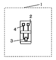
図1、図2、図3は本発明の実施の形態1による電極基板の正面図、断面図と斜視図を示す。図1は図2のA−A’断面における電極基板1の断面を正面から見た正面図である。図2は、図3のB−B’断面における、電極基板1の断面図である。図3は、電極基板1の斜面図である。
(Embodiment 1)
1, 2, and 3 are a front view, a cross-sectional view, and a perspective view of an electrode substrate according to
電極基板1は、基板2と、基板2の上に設けられた電極3と、電極3と導通する端子4と、電極3の上方に設けられたカバー5で構成されている。カバー5と電極3の間にはス
ペーサー19により隙間が作製されており、空隙6と、空隙6を挟んで外部と接続している開口7、8が設けられている。
The
電極3がカバー5で保護されているため、電極基板1を操作する際に、直接電極3に指が触れない。また、本電極基板1の電極3を流れのある被検査溶液に浸した際、開口7より被検査溶液が流入し、開口8へ流出する方向の流れ、または、開口8から開口7へ向かう流れにより、空隙6と開口7、8が被検査溶液の通路となり、電極3近傍への微生物や粒子の連続的な供給が可能となり、電極感度の低下を抑えることができる。
Since the
次に、本発明の実施の形態1による電極基板1を用いた測定装置23及びその動作を説明する。
Next, the
図4は、本発明の測定装置23の構成を示す図である。図4において、10は測定対象物が含まれる被検査溶液11を保持する溶液保持部、24は、電極基板1の端子4から導通を得るとともに電極基板1を固定する接続部、1は微細パターンが施された電極3を含む電極基板、12は電圧印加部、13は電極反応を測定する測定部、14は測定装置全体の制御や測定した応答の演算を行う制御演算部である。
FIG. 4 is a diagram showing the configuration of the
電極基板1は、初めに、接続部24に挿入され、端子4を介して電極3と電圧印加部12および測定部13は電気的に接続され、同時に固定される。
The
電極基板1は、微生物が含まれた被検査溶液11を保持した溶液保持部10内に浸漬される。溶液保持部10は、マグネチックスターラーなどの攪拌手段15を設けることができる。被検査溶液11を溶液保持部10内で攪拌することにより被検査溶液11内での測定対象物濃度を均一にすることができ、かつ、多くの測定対象物を電極近傍に導くことができるため、より効率的測定でき、測定時間の短縮や測定感度低下の抑制が可能である。
The
攪拌方法は、選択可能であり、マグネチックスターラーによる攪拌、棒状の攪拌器具によりかき混ぜる方法、溶液保持部10自体が回転することによる攪拌等がある。攪拌速度は、被検査溶液中の粒子や微生物が十分還流する速度に設定する。
The stirring method can be selected, and includes a stirring method using a magnetic stirrer, a stirring method using a bar-like stirring device, and a stirring method by rotating the
電圧印加部12は電極に所定の電圧を印加し、被検査溶液11中の測定対象物の電極反応を、測定部13により測定、測定した値は制御演算部14に渡る。また、制御演算部14は、電圧印加部12を制御し、電極に特定の電圧を印加する。さらに、制御演算部14は、測定部13が測定したデータを受け取り、被検査溶液中に含まれる測定対象物の濃度演算が行なわれる。演算結果は、逐次メモリに格納、または、LCDなどの表示部16に結果表示を行う。
The voltage application unit 12 applies a predetermined voltage to the electrodes, and the measurement unit 13 measures the electrode reaction of the measurement target in the solution under
次に、電極基板1の寸法を説明する。電極3とカバー5間の距離は、1mm以上5mm以下が好ましい。1mm以下では、電極3への被検査溶液の接触が阻害され、電極感度が低下するが、1mm以上5mm以下では、電極3近傍に被検査溶液の流れが形成されるため、被検査溶液が循環し絶えず新しい被検査を電極3に供給でき、電極感度の低下を抑えることができる。
Next, the dimensions of the
一方、本発明に用いた溶液保持部10は、径20mmの円柱型セルであり、電極は、水面に挿入されている。電極3とカバー5間の距離が5mmを超える電極カバーを装着すると、カバーがセル底部に位置する攪拌手段15の上部を覆ってしまう。攪拌機能がカバー5により阻害されてしまい、新しい被検査の電極3への供給効率が低下するため、電極感度の低下を招く。
On the other hand, the
カバー5の面積は、電極3の面積と等しいまたは大きいことが望ましい。かかる構成では、電極3への粉塵の接触を避けることができ、電極3表面への汚れの付着や電極3の損傷を防ぐことができる。よって、センサの保存を容易にし、また、測定環境も限定されない。
The area of the
次に、電極基板1の材料及び作成方法を説明する。本発明の実施の形態に示す電極基板1は、基板2に電極3および端子4をパターニングする工程、電極3上にカバー5を固定する工程を経て、作製される。電極3および端子4をパターニングする工程は、選択した材料で所望のパターンを形成できれば、フォトリソグラフィー、レーザー加工、スクリーン印刷、インクジェット印刷など、生産性やコストなどを勘案して最も適切な加工法が選択可能である。
Next, the material and production method of the
電極3上にカバー5を固定する工程は、図1に示すように、電極3とカバー5とをスペーサー19を介して固定してもよい。固定方法は、接着剤を使用しない工法が好ましく、熱による融着、超音波接合、UVランプによる光接合、ネジ止め型などから選択される。
In the step of fixing the
本発明における基板2は、樹脂基板を用いたが、絶縁性の材料であればいずれも使用可能であり、例えば、ガラス、セラミックなど基板材料の使用を妨げるものではない。また、電極3は導電性の材料であればいずれも使用可能であり、Au、Ag、Alなどの金属粒子含有の導電性ペースト、カーボンなども選択可能である。
As the
(実施の形態2)
図5は本発明の実施の形態2による電極基板1の断面図である。実施の形態1と同様の構造を持つ電極基板であるが、カバー5は、基板2の厚みと等しい、もしくは、基板厚みよりも微小に大きい凹部22を持ち、凹部22に基板2が挟まれることでカバー5に固定化される。これにより、溝22からの基板2の取り外しが可能となり、また、カバーの大きさが限定されないため、基板2が小さい場合でも指で持ちやすく、電極のハンドリングも向上する。さらに、接着剤を使用しないため、被検査溶液へ接着剤成分が溶け出し夾雑物質となる可能性を抑えることができる。
(Embodiment 2)
FIG. 5 is a sectional view of
凹部22の厚みの許容差は、基板2がカバー5に固定されるなら任意であるが、基板2の厚み+0mmから基板2の厚み+0.2mmが好ましい。基板2、カバー5の材料は、曲げや伸縮が可能な樹脂材料が適する。上記材料を用いると上記許容差に縛られず、凹部22の厚みが基板2の厚みより小さい場合もはめ込むことができる。凹部22の深さは基板2がカバー5に固定されるなら任意であるが、1mm以上5mm以下が固定の確実性の点から好ましい。
The tolerance of the thickness of the
本発明の実施の形態2による電極基板1を用いた電極操作及び動作、測定装置は実施の形態1における電極基板1と同様である。
The electrode operation, operation, and measuring apparatus using the
(実施の形態3)
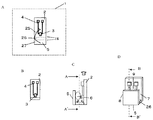
図6は本発明の実施の形態3による電極基板1の概略図である。
(Embodiment 3)
FIG. 6 is a schematic view of an
図6Aは、図6Cの展開図である。図6Bは図6CのA−A’断面におけるカバー付電極基板1の断面図である。図6Cは、図6DのB−B’断面における、電極基板1の断面図である。図6Dは、電極基板1の斜面図である。
FIG. 6A is a development view of FIG. 6C. FIG. 6B is a cross-sectional view of the electrode substrate with
カバー5が基板2と一体になっていることが実施の形態1と相違し、以下では、その相違点のみを説明する。
Unlike the first embodiment, the
本実施の形態による電極基板1の基板2は、図6Aに示すように、電極3と端子4がパターニングされる電極配置部25と、必要に応じて形成されるおりしろ部26と、カバー5となるカバー部27からなる。電極配置部25とおりしろ部26、および、おりしろ部26とカバー部27は、それぞれ所定の角度で曲げられ、電極配置部25とカバー部27が対向している。
As shown in FIG. 6A, the
また、図6Cを参照すると、おりしろ部26の厚み分だけカバー5と電極3の間には空隙6が形成され、上面視でカバー5のおりしろ部26を除く3方向に開口7、8、9が形成されている。かかる構成により、カバー部27であるカバー5が電極3の上方に位置し、電極3がカバー5で保護され、また、本カバー付電極基板1の電極3を流れのある被検査溶液に浸した際、開口7、8、9から空隙6へと被検査溶液が流入・流出する方向の流れが生じる。
Referring to FIG. 6C, a
これらの構造により、電極操作の際、電極3に指が触れず、かつ、電極近傍への被検査溶液の供給を連続的に行うことができる。また、電極とカバーを一枚の同一基板上に作製でき、カバー作製に要するのは折り曲げ工程のみであるため、作業工程の簡略化や基板材料費の削減が期待できる。さらに、作製時に接着剤を使用しないため、被検査溶液への夾雑物質の流出を最低限に抑えることができ、測定値が安定する。
With these structures, the
電極基板1の作製方法は、基板2に電極3および端子4をパターニングする工程、基板2の電極配置部25とおりしろ部26とカバー部27の間に2つの折り曲げ線18を入れる工程、折り曲げ線18でカバー5が電極3の上方に配置するように折り曲げる工程を経て、作製される。
The method of manufacturing the
実施の形態3で使用する基板2の材料は、基板上へ電極作成後に圧力や熱などの外部からの力を加えることで、折り曲げ形成が可能な樹脂材料を用いる。厚みは、加工性の良い500mm以下の樹脂材料が適する。
The material of the
図6において、2つの折り曲げ線18の間のおりしろ部26の長さと、電極配置部25とおりしろ部26、および、おりしろ部26とカバー部27の曲げ角度α、βは、電極3とカバー5の間の電極3とカバー5間の距離が1mm以上となるよう選ばれる。おりしろ部の長さは好適には1mm以上10mm以下である。
In FIG. 6, the length of the
曲げ角度α、βはそれぞれ0°から180°であり、好適には90°である。カバー部27は、少なくとも電極3の表面積と等しい、または大きい表面積を持つことが電極3への指の接触回避の点から望ましい。
The bending angles α and β are each 0 ° to 180 °, preferably 90 °. The
本実施形態の別の一例としておりしろ部26を省略した電極基板1を図7に示す。図7Aは、図7Bの展開図である。基板2は、電極3と端子4がパターニングされる電極配置部25と、カバー5となるカバー部27からなる。電極配置部25とカバー部27の間に一つの折り曲げ線18が形成され、30°の角度で曲げられ、カバー部27が電極3を覆い、空隙6を形成している。曲げ角度は、90°以下から選択される。
As another example of this embodiment, an
本発明の実施の形態3による電極基板1を用いた電極操作及び動作、測定装置は実施の形態1における電極基板1と同様である。図8には作製方法のフローと作製した物を示す図を記載した。
The electrode operation, operation, and measuring apparatus using the
また、図8に示すように、端子4間領域をおりしろ部26およびカバー部27として折り返し、カバー5を作製することにより、一つの基板材料シートから取れるカバー付電極基板1の個数を最大にすることができる。これにより、高価な樹脂基板を用いた際でも、
材料コストの大幅な削減が見込まれる。
Further, as shown in FIG. 8, the region between the
Significant reductions in material costs are expected.
(実施の形態4)
図9、図10は本発明の実施の形態4による電極基板の概略図である。図9A、9Bは、それぞれ、カバー5がメッシュ状の開口20を持つ電極基板1の斜面図と断面図であり、図10A、10Bは、それぞれ、カバー5に開口21を持つ電極基板1の斜面図と断面図である。
(Embodiment 4)
9 and 10 are schematic views of an electrode substrate according to
実施の形態1と同様の構造を持つ電極基板であるが、電極3とカバー5間の距離が1mm〜5mmの条件下において、カバー5は10mm径以上のメッシュ構造20により構成
されている、または、5mm径以下の開口21を最低一つ以上有していることを特徴とする。10mmの開口は被検査溶液中の微生物・微粒子の径よりも大きく、5mmの開口は
、電極3とカバー5間の距離が1mmを有する電極基板1を手で操作した際に、指が電極部や電極パターン面に接触しない大きさの上限である。
Although the electrode substrate has the same structure as that of the first embodiment, the
なお、開口の形状は円形にこだわらない。開口を形成できる多角形であればよい。 Note that the shape of the opening is not limited to a circle. Any polygon that can form an opening may be used.
カバー5は、これにより、電極に対して水平方向の開口7、8を介する、電極に対して水平方向の流れだけでなく、電極に対して垂直方向への被検査溶液供給も可能となり、電極近傍へのより効果的な被検査溶液の供給と感度の上昇が期待できる。
Thus, the
電極操作の際、カバー5と空隙6、開口7〜9、20、21により、電極3に指が触れず、かつ、連続的な電極近傍への被検査溶液の供給が可能となる。
When the electrode is operated, the
10mm以上のメッシュの材料は、生体分子や粒子が付着しにくいもの、5mm以下の
開口を持つカバーは、加工性の良い樹脂材料とする。
The mesh material of 10 mm or more is difficult for biomolecules and particles to adhere to it, and the cover having an opening of 5 mm or less is a resin material with good workability.
本発明の実施の形態4による電極基板1を用いた電極操作及び動作、測定装置は実施の形態1における電極基板1と同様である。
The electrode operation, operation and measurement apparatus using the
次に、実施の形態3に示した電極基板1、実施の形態1に示した測定装置23を用い、DEPIM法(特許文献1)により被検査溶液中の細菌の電気化学応答をモニターした結果を示す。
Next, using the
図4に示すように、電極基板1を被検査溶液11に浸し、攪拌手段15であるスターラーにより攪拌しながら、電圧印加部12より電極3へ特定の周波数と電圧をもった交流電圧を印加した。
As shown in FIG. 4, the
図11は、電極3の一例を示す部分斜視図である。図11において、2は基板、17a、17bは基板2上に形成され一対の極をなす電極である。電極17a、17b間に交流電圧を印加することにより、電極17a、17b間に不平等電界が誘起され、微生物を誘電泳動し17a、17b間のギャップに捕集する。それと同時に、測定部において17a、17b間のギャップに捕集した微生物の応答を測定した。測定結果は演算部14に渡り、電極17a、17b間のインピーダンスを算出、インピーダンスより被検査溶液中に含まれる微生物濃度を算出した。
FIG. 11 is a partial perspective view showing an example of the
被検査溶液には、4.1×10⁶(cfu/mL)に調製した大腸菌懸濁液を5mL使用した。 As the test solution, 5 mL of the E. coli suspension prepared to 4.1 × 10 6 (cfu / mL) was used.
電極とカバーの間の距離を0.5mm、1mm、2mm、5mmとしたカバー付電極基板を作製し、それぞれの距離に対する電極感度をプロットした。カバーがない時の電極基板と同程度の感度を得るために、電極とカバーの間の距離と電極感度の関係を検証した。カバーの寸法は、横10.9mm、縦8mm,電極基板の大きさは、横10.9mm、縦24mmとした。 An electrode substrate with a cover having a distance between the electrode and the cover of 0.5 mm, 1 mm, 2 mm, and 5 mm was produced, and the electrode sensitivity with respect to each distance was plotted. In order to obtain the same sensitivity as that of the electrode substrate without the cover, the relationship between the distance between the electrode and the cover and the electrode sensitivity was verified. The dimensions of the cover were 10.9 mm wide and 8 mm long, and the size of the electrode substrate was 10.9 mm wide and 24 mm long.
図12は、カバー無電極基板とカバー付電極基板の感度を比較するために、カバー無し電極基板を用いた測定の感度をcontrol(100%)と規定し、カバー付電極基板の測定感度の割合をプロットした。 FIG. 12 shows that the sensitivity of measurement using the electrode substrate without cover is defined as control (100%) in order to compare the sensitivity of the electrode substrate with cover and the electrode substrate with cover. Was plotted.
電極とカバーの間の距離が1mm以下の時は、カバー無電極感度の50〜60%であったが、電極とカバーの間の距離を1mm以上に設定すると、カバーがないときの80%の感度を得ることができた。よって、電極とカバーの間の距離が1mm以上である本発明の電極基板1は、電極3への被検査溶液の供給が十分行なわれ、感度の低下を抑えることが明らかとなった。
When the distance between the electrode and the cover was 1 mm or less, it was 50 to 60% of the cover no-electrode sensitivity. However, when the distance between the electrode and the cover was set to 1 mm or more, it was 80% when there was no cover. Sensitivity could be obtained. Therefore, it has been clarified that the
本発明にかかる電極基板は、電極操作の際に、油脂や粉塵の付着、電極の損傷を抑え、かつ、被検査溶液の電極部分への供給が可能となり、安定した応答を得られる。よって、電極を利用した微生物や微粒子の操作および測定が可能な電極基板等として有用である。 The electrode substrate according to the present invention suppresses adhesion of fats and oils and dust and electrode damage during electrode operation, and can supply a solution to be inspected to the electrode portion, thereby obtaining a stable response. Therefore, it is useful as an electrode substrate or the like capable of manipulating and measuring microorganisms and fine particles using electrodes.
1 電極基板
2 基板
3 電極
4 端子
5 カバー
6 空隙
7,8,9 開口
10 溶液保持部
11 被検査溶液
12 電圧印加部
13 測定部
14 制御演算部
15 攪拌手段
16 表示部
17a,17b 電極構造
18 折り曲げ線
19 スペーサー
20 メッシュ型カバーの開口
21 開口
22 凹部(溝)
23 測定装置
24 接続部
25 電極配置部
26 おりしろ部
27 カバー部
DESCRIPTION OF
23
Claims (3)
導電性を持ち前記基板の上に設けられた電極と、
前記電極につながり前記電極からの信号を伝達する端子と、
前記電極の前記基板とは対向する方向に設けられたカバーと、
を有し、
前記カバーが空隙を介して前記電極の一部または全部を覆い、
前記空隙が少なくとも2つ以上の開口により外部と接続しており、
前記開口が空隙を挟む位置に配置され、
前記開口が対向する方向が、基板に対して水平であり、
前記電極と前記カバーの距離が1mm以上5mm以下であり、
前記開口より被検査溶液が前記空隙へ流出入することで、前記電極近傍へ前記被検査溶液を連続的に供給すること、
を特徴とする前記電極を用いて前記被検査溶液中の反応を測定する電極基板。 At least with the substrate,
An electrode having conductivity and provided on the substrate;
A terminal connected to the electrode and transmitting a signal from the electrode;
A cover provided in a direction facing the substrate of the electrode ;
Have
The cover covers part or all of the electrode through a gap;
The gap is connected to the outside through at least two openings;
The opening is disposed at a position sandwiching the gap ,
A direction in which the opening faces is horizontal to the substrate;
The distance between the electrode and the cover is 1 mm or more and 5 mm or less,
The solution to be inspected flows out of the opening into the gap to continuously supply the solution to be inspected to the vicinity of the electrode;
An electrode substrate for measuring a reaction in the solution to be inspected using the electrode.
Priority Applications (1)
| Application Number | Priority Date | Filing Date | Title |
|---|---|---|---|
| JP2007240565A JP5205889B2 (en) | 2007-09-18 | 2007-09-18 | Electrode substrate and microbe / particle measuring device using the same |
Applications Claiming Priority (1)
| Application Number | Priority Date | Filing Date | Title |
|---|---|---|---|
| JP2007240565A JP5205889B2 (en) | 2007-09-18 | 2007-09-18 | Electrode substrate and microbe / particle measuring device using the same |
Publications (3)
| Publication Number | Publication Date |
|---|---|
| JP2009069096A JP2009069096A (en) | 2009-04-02 |
| JP2009069096A5 JP2009069096A5 (en) | 2010-10-28 |
| JP5205889B2 true JP5205889B2 (en) | 2013-06-05 |
Family
ID=40605497
Family Applications (1)
| Application Number | Title | Priority Date | Filing Date |
|---|---|---|---|
| JP2007240565A Expired - Fee Related JP5205889B2 (en) | 2007-09-18 | 2007-09-18 | Electrode substrate and microbe / particle measuring device using the same |
Country Status (1)
| Country | Link |
|---|---|
| JP (1) | JP5205889B2 (en) |
Families Citing this family (1)
| Publication number | Priority date | Publication date | Assignee | Title |
|---|---|---|---|---|
| JP7278755B2 (en) * | 2018-11-26 | 2023-05-22 | Nissha株式会社 | Photomask and collection unit base |
Family Cites Families (11)
| Publication number | Priority date | Publication date | Assignee | Title |
|---|---|---|---|---|
| JP3365184B2 (en) * | 1996-01-10 | 2003-01-08 | 松下電器産業株式会社 | Biosensor |
| JPH10311817A (en) * | 1997-05-09 | 1998-11-24 | Nok Corp | Biosensor |
| JP3869687B2 (en) * | 2001-06-26 | 2007-01-17 | 独立行政法人科学技術振興機構 | Microbial activity measuring apparatus and microbial activity measuring method |
| JP3693241B2 (en) * | 2001-07-19 | 2005-09-07 | 純也 末廣 | Oral hygiene state inspection device and method for measuring the number of microorganisms in the oral cavity |
| EP1484603A4 (en) * | 2002-03-08 | 2007-11-21 | Arkray Inc | Analyzer having information recognizing function, analytic tool for use therein, and unit of analyzer and analytic tool |
| JP2004004017A (en) * | 2002-03-29 | 2004-01-08 | Nissha Printing Co Ltd | Biosensor and manufacturing method of the biosensor |
| JP2004069430A (en) * | 2002-08-05 | 2004-03-04 | Mitsubishi Kagaku Iatron Inc | Chip for electrophoresis, method for production thereof and method for separating substance |
| JP2006010352A (en) * | 2004-06-22 | 2006-01-12 | Sumitomo Electric Ind Ltd | Sensor chip and its manufacturing method |
| JP4740664B2 (en) * | 2005-07-04 | 2011-08-03 | パナソニック株式会社 | Microbial test chip and microbiological test method |
| JP4649594B2 (en) * | 2006-02-03 | 2011-03-09 | 独立行政法人産業技術総合研究所 | Biosensor and manufacturing method thereof |
| JP2007178446A (en) * | 2007-03-05 | 2007-07-12 | Therasense Inc | Biosensor |
-
2007
- 2007-09-18 JP JP2007240565A patent/JP5205889B2/en not_active Expired - Fee Related
Also Published As
| Publication number | Publication date |
|---|---|
| JP2009069096A (en) | 2009-04-02 |
Similar Documents
| Publication | Publication Date | Title |
|---|---|---|
| Shin et al. | Label‐free and regenerative electrochemical microfluidic biosensors for continual monitoring of cell secretomes | |
| US9448223B2 (en) | Impedance-based sensing of adherent cells on a digital microfluidic device | |
| Lazar et al. | Hampering of the stability of gold electrodes by ferri-/ferrocyanide redox couple electrolytes during electrochemical impedance spectroscopy | |
| Kuo et al. | Improving sensitivity of a miniaturized label-free electrochemical biosensor using zigzag electrodes | |
| CN100535649C (en) | Microelectrode biosensing chip of 3D nanogap mesh array | |
| JP5675594B2 (en) | Method for detecting chemical or biological species and electrode arrangement therefor | |
| CN111295581B (en) | pH control for analyte detection | |
| Wang et al. | Microfabricated electrophoresis chip for bioassay of renal markers | |
| JP5384479B2 (en) | Fine particle measuring apparatus and fine particle measuring method | |
| JPWO2009037804A1 (en) | Fine particle measuring apparatus and fine particle measuring method | |
| Li et al. | Band electrodes in sensing applications: response characteristics and band fabrication methods | |
| CN205844251U (en) | Detector electrode structure and detection orifice plate | |
| Juskova et al. | Fabrication and characterization of solid mercury amalgam electrodes for protein analysis | |
| García et al. | Copper nanowires immobilized on the boards of microfluidic chips for the rapid and simultaneous diagnosis of galactosemia diseases in newborn urine samples | |
| US10612078B2 (en) | Integrated electrochemical nucleic acid based sensors and related platforms | |
| Houssin et al. | Electrochemical detection | |
| EP3216076B1 (en) | Method of using electrochemical test elements having multiple electrode arrangements | |
| Gu et al. | Cellular electrical impedance spectroscopy: an emerging technology of microscale biosensors | |
| JP5205889B2 (en) | Electrode substrate and microbe / particle measuring device using the same | |
| Gardner et al. | Development of a microelectrode array sensing platform for combination electrochemical and spectrochemical aqueous ion testing | |
| Ino et al. | Droplet array on local redox cycling-based electrochemical (LRC-EC) chip device | |
| JP2022010070A (en) | Sensor assembly and method of using same | |
| WO2009093458A1 (en) | Microparticle measurement device and microparticle measurement method | |
| JP2009069096A5 (en) | ||
| KR101924415B1 (en) | Multiple impedance measurement apparatus and method |
Legal Events
| Date | Code | Title | Description |
|---|---|---|---|
| A521 | Written amendment |
Free format text: JAPANESE INTERMEDIATE CODE: A523 Effective date: 20100913 |
|
| A621 | Written request for application examination |
Free format text: JAPANESE INTERMEDIATE CODE: A621 Effective date: 20100913 |
|
| RD01 | Notification of change of attorney |
Free format text: JAPANESE INTERMEDIATE CODE: A7421 Effective date: 20101013 |
|
| A977 | Report on retrieval |
Free format text: JAPANESE INTERMEDIATE CODE: A971007 Effective date: 20120509 |
|
| A131 | Notification of reasons for refusal |
Free format text: JAPANESE INTERMEDIATE CODE: A131 Effective date: 20120710 |
|
| A521 | Written amendment |
Free format text: JAPANESE INTERMEDIATE CODE: A523 Effective date: 20120830 |
|
| RD01 | Notification of change of attorney |
Free format text: JAPANESE INTERMEDIATE CODE: A7421 Effective date: 20121213 |
|
| TRDD | Decision of grant or rejection written | ||
| A01 | Written decision to grant a patent or to grant a registration (utility model) |
Free format text: JAPANESE INTERMEDIATE CODE: A01 Effective date: 20130122 |
|
| A61 | First payment of annual fees (during grant procedure) |
Free format text: JAPANESE INTERMEDIATE CODE: A61 Effective date: 20130204 |
|
| FPAY | Renewal fee payment (event date is renewal date of database) |
Free format text: PAYMENT UNTIL: 20160301 Year of fee payment: 3 |
|
| R151 | Written notification of patent or utility model registration |
Ref document number: 5205889 Country of ref document: JP Free format text: JAPANESE INTERMEDIATE CODE: R151 |
|
| FPAY | Renewal fee payment (event date is renewal date of database) |
Free format text: PAYMENT UNTIL: 20160301 Year of fee payment: 3 |
|
| S111 | Request for change of ownership or part of ownership |
Free format text: JAPANESE INTERMEDIATE CODE: R313113 |
|
| R350 | Written notification of registration of transfer |
Free format text: JAPANESE INTERMEDIATE CODE: R350 |
|
| S111 | Request for change of ownership or part of ownership |
Free format text: JAPANESE INTERMEDIATE CODE: R313113 |
|
| R350 | Written notification of registration of transfer |
Free format text: JAPANESE INTERMEDIATE CODE: R350 |
|
| S111 | Request for change of ownership or part of ownership |
Free format text: JAPANESE INTERMEDIATE CODE: R313113 |
|
| R350 | Written notification of registration of transfer |
Free format text: JAPANESE INTERMEDIATE CODE: R350 |
|
| R250 | Receipt of annual fees |
Free format text: JAPANESE INTERMEDIATE CODE: R250 |
|
| R250 | Receipt of annual fees |
Free format text: JAPANESE INTERMEDIATE CODE: R250 |
|
| R250 | Receipt of annual fees |
Free format text: JAPANESE INTERMEDIATE CODE: R250 |
|
| S533 | Written request for registration of change of name |
Free format text: JAPANESE INTERMEDIATE CODE: R313533 |
|
| R350 | Written notification of registration of transfer |
Free format text: JAPANESE INTERMEDIATE CODE: R350 |
|
| LAPS | Cancellation because of no payment of annual fees |