JP5201538B2 - Magnetic random access memory - Google Patents
Magnetic random access memory Download PDFInfo
- Publication number
- JP5201538B2 JP5201538B2 JP2009502473A JP2009502473A JP5201538B2 JP 5201538 B2 JP5201538 B2 JP 5201538B2 JP 2009502473 A JP2009502473 A JP 2009502473A JP 2009502473 A JP2009502473 A JP 2009502473A JP 5201538 B2 JP5201538 B2 JP 5201538B2
- Authority
- JP
- Japan
- Prior art keywords
- magnetization
- region
- braking
- magnetization fixed
- random access
- Prior art date
- Legal status (The legal status is an assumption and is not a legal conclusion. Google has not performed a legal analysis and makes no representation as to the accuracy of the status listed.)
- Active
Links
- 230000005291 magnetic effect Effects 0.000 title claims description 93
- 230000005415 magnetization Effects 0.000 claims description 300
- 230000005294 ferromagnetic effect Effects 0.000 claims description 8
- 230000002441 reversible effect Effects 0.000 claims description 7
- 229910052763 palladium Inorganic materials 0.000 claims description 5
- 229910052697 platinum Inorganic materials 0.000 claims description 5
- 229910052796 boron Inorganic materials 0.000 claims description 2
- 238000013016 damping Methods 0.000 claims 2
- 238000000034 method Methods 0.000 description 12
- 239000002184 metal Substances 0.000 description 10
- 229910052751 metal Inorganic materials 0.000 description 10
- 230000004888 barrier function Effects 0.000 description 9
- 230000000694 effects Effects 0.000 description 9
- 238000010586 diagram Methods 0.000 description 7
- 230000004048 modification Effects 0.000 description 7
- 238000012986 modification Methods 0.000 description 7
- 238000002347 injection Methods 0.000 description 5
- 239000007924 injection Substances 0.000 description 5
- 230000005381 magnetic domain Effects 0.000 description 5
- 230000021715 photosynthesis, light harvesting Effects 0.000 description 5
- 230000007704 transition Effects 0.000 description 5
- 230000009471 action Effects 0.000 description 4
- 239000000696 magnetic material Substances 0.000 description 4
- 238000005036 potential barrier Methods 0.000 description 4
- 238000012546 transfer Methods 0.000 description 4
- 230000008859 change Effects 0.000 description 3
- 238000013461 design Methods 0.000 description 3
- 239000000463 material Substances 0.000 description 3
- 229910019236 CoFeB Inorganic materials 0.000 description 2
- 229910001030 Iron–nickel alloy Inorganic materials 0.000 description 2
- 229910045601 alloy Inorganic materials 0.000 description 2
- 239000000956 alloy Substances 0.000 description 2
- 239000004020 conductor Substances 0.000 description 2
- 229910052802 copper Inorganic materials 0.000 description 2
- 230000000149 penetrating effect Effects 0.000 description 2
- 229910052715 tantalum Inorganic materials 0.000 description 2
- 229910018072 Al 2 O 3 Inorganic materials 0.000 description 1
- 229910003321 CoFe Inorganic materials 0.000 description 1
- 230000005290 antiferromagnetic effect Effects 0.000 description 1
- 239000002885 antiferromagnetic material Substances 0.000 description 1
- 239000002772 conduction electron Substances 0.000 description 1
- 230000003111 delayed effect Effects 0.000 description 1
- 230000001747 exhibiting effect Effects 0.000 description 1
- 230000005350 ferromagnetic resonance Effects 0.000 description 1
- 238000009434 installation Methods 0.000 description 1
- 230000010354 integration Effects 0.000 description 1
- 230000003993 interaction Effects 0.000 description 1
- 150000002500 ions Chemical class 0.000 description 1
- 229910052742 iron Inorganic materials 0.000 description 1
- 238000007562 laser obscuration time method Methods 0.000 description 1
- 239000011159 matrix material Substances 0.000 description 1
- 229910052759 nickel Inorganic materials 0.000 description 1
- 239000002245 particle Substances 0.000 description 1
- 238000011160 research Methods 0.000 description 1
- 230000000630 rising effect Effects 0.000 description 1
Images


Classifications
-
- G—PHYSICS
- G11—INFORMATION STORAGE
- G11C—STATIC STORES
- G11C11/00—Digital stores characterised by the use of particular electric or magnetic storage elements; Storage elements therefor
- G11C11/02—Digital stores characterised by the use of particular electric or magnetic storage elements; Storage elements therefor using magnetic elements
- G11C11/16—Digital stores characterised by the use of particular electric or magnetic storage elements; Storage elements therefor using magnetic elements using elements in which the storage effect is based on magnetic spin effect
- G11C11/161—Digital stores characterised by the use of particular electric or magnetic storage elements; Storage elements therefor using magnetic elements using elements in which the storage effect is based on magnetic spin effect details concerning the memory cell structure, e.g. the layers of the ferromagnetic memory cell
-
- G—PHYSICS
- G11—INFORMATION STORAGE
- G11C—STATIC STORES
- G11C11/00—Digital stores characterised by the use of particular electric or magnetic storage elements; Storage elements therefor
- G11C11/02—Digital stores characterised by the use of particular electric or magnetic storage elements; Storage elements therefor using magnetic elements
- G11C11/16—Digital stores characterised by the use of particular electric or magnetic storage elements; Storage elements therefor using magnetic elements using elements in which the storage effect is based on magnetic spin effect
- G11C11/165—Auxiliary circuits
- G11C11/1659—Cell access
-
- G—PHYSICS
- G11—INFORMATION STORAGE
- G11C—STATIC STORES
- G11C11/00—Digital stores characterised by the use of particular electric or magnetic storage elements; Storage elements therefor
- G11C11/02—Digital stores characterised by the use of particular electric or magnetic storage elements; Storage elements therefor using magnetic elements
- G11C11/16—Digital stores characterised by the use of particular electric or magnetic storage elements; Storage elements therefor using magnetic elements using elements in which the storage effect is based on magnetic spin effect
- G11C11/165—Auxiliary circuits
- G11C11/1675—Writing or programming circuits or methods
-
- G—PHYSICS
- G11—INFORMATION STORAGE
- G11C—STATIC STORES
- G11C19/00—Digital stores in which the information is moved stepwise, e.g. shift registers
- G11C19/02—Digital stores in which the information is moved stepwise, e.g. shift registers using magnetic elements
- G11C19/08—Digital stores in which the information is moved stepwise, e.g. shift registers using magnetic elements using thin films in plane structure
- G11C19/0808—Digital stores in which the information is moved stepwise, e.g. shift registers using magnetic elements using thin films in plane structure using magnetic domain propagation
-
- H—ELECTRICITY
- H10—SEMICONDUCTOR DEVICES; ELECTRIC SOLID-STATE DEVICES NOT OTHERWISE PROVIDED FOR
- H10B—ELECTRONIC MEMORY DEVICES
- H10B61/00—Magnetic memory devices, e.g. magnetoresistive RAM [MRAM] devices
- H10B61/20—Magnetic memory devices, e.g. magnetoresistive RAM [MRAM] devices comprising components having three or more electrodes, e.g. transistors
- H10B61/22—Magnetic memory devices, e.g. magnetoresistive RAM [MRAM] devices comprising components having three or more electrodes, e.g. transistors of the field-effect transistor [FET] type
-
- H—ELECTRICITY
- H10—SEMICONDUCTOR DEVICES; ELECTRIC SOLID-STATE DEVICES NOT OTHERWISE PROVIDED FOR
- H10N—ELECTRIC SOLID-STATE DEVICES NOT OTHERWISE PROVIDED FOR
- H10N50/00—Galvanomagnetic devices
- H10N50/10—Magnetoresistive devices
Landscapes
- Engineering & Computer Science (AREA)
- Computer Hardware Design (AREA)
- Mram Or Spin Memory Techniques (AREA)
- Hall/Mr Elements (AREA)
- Magnetic Heads (AREA)
Description
本発明は、磁気ランダムアクセスメモリ(MRAM: Magnetic Random Access Memory)に関する。特に、本発明は、磁壁移動方式のMRAMに関する。
本出願は、2007年3月7日に出願された日本国特許出願2007−056693を基礎とする優先権を主張し、その開示の全てをここに取り込む。The present invention relates to a magnetic random access memory (MRAM). In particular, the present invention relates to a domain wall motion type MRAM.
This application claims the priority on the basis of the Japan patent application 2007-056693 for which it applied on March 7, 2007, and takes in those the indications of all here.
MRAMは、高集積・高速動作の観点から有望な不揮発性メモリである。MRAMにおいては、TMR(Tunnel MagnetoResistance)効果などの「磁気抵抗効果」を示す磁気抵抗素子が利用される。その磁気抵抗素子には、例えばトンネルバリヤ層が2層の強磁性層で挟まれた磁気トンネル接合(MTJ; Magnetic Tunnel Junction)が形成される。その2層の強磁性層は、磁化の向きが固定された磁化固定層(ピン層)と、磁化の向きが反転可能な磁化自由層(フリー層)から構成される。 MRAM is a promising nonvolatile memory from the viewpoint of high integration and high-speed operation. In the MRAM, a magnetoresistive element exhibiting a “magnetoresistance effect” such as a TMR (Tunnel MagnetoResistance) effect is used. In the magnetoresistive element, for example, a magnetic tunnel junction (MTJ) in which a tunnel barrier layer is sandwiched between two ferromagnetic layers is formed. The two ferromagnetic layers are composed of a magnetization fixed layer (pinned layer) whose magnetization direction is fixed and a magnetization free layer (free layer) whose magnetization direction can be reversed.
ピン層とフリー層の磁化の向きが“反平行”である場合のMTJの抵抗値(R+ΔR)は、磁気抵抗効果により、それらが“平行”である場合の抵抗値(R)よりも大きくなることが知られている。MRAMは、このMTJを有する磁気抵抗素子をメモリセルとして用い、その抵抗値の変化を利用することによってデータを不揮発的に記憶する。例えば、反平行状態はデータ“1”に対応付けられ、平行状態はデータ“0”に対応付けられる。メモリセルに対するデータの書き込みは、フリー層の磁化の向きを反転させることによって行われる。 The resistance value (R + ΔR) of the MTJ when the magnetization directions of the pinned layer and the free layer are “anti-parallel” is larger than the resistance value (R) when they are “parallel” due to the magnetoresistance effect. It is known. The MRAM uses the magnetoresistive element having the MTJ as a memory cell, and stores data in a nonvolatile manner by utilizing the change in the resistance value. For example, the antiparallel state is associated with data “1”, and the parallel state is associated with data “0”. Data is written to the memory cell by reversing the magnetization direction of the free layer.
MRAMに対するデータの書き込み方法として、従来、「アステロイド方式」や「トグル方式」が知られている。これらの書き込み方式によれば、メモリセルサイズにほぼ反比例して、フリー層の磁化を反転させるために必要な反転磁界が大きくなる。つまり、メモリセルが微細化されるにつれて、書き込み電流が増加する傾向にある。 Conventionally, “asteroid method” and “toggle method” are known as methods of writing data to the MRAM. According to these write methods, the reversal magnetic field necessary for reversing the magnetization of the free layer increases in inverse proportion to the memory cell size. That is, the write current tends to increase as the memory cell is miniaturized.
微細化に伴う書き込み電流の増加を抑制することができる書き込み方式として、「スピン注入(spin transfer)方式」が提案されている(例えば、特開2005−93488号公報、及び、Yagami and Suzuki,Research Trends in Spin Transfer Magnetization Switching,日本応用磁気学会誌,Vol.28,No.9,2004を参照)。スピン注入方式によれば、強磁性導体にスピン偏極電流(spin-polarized current)が注入され、その電流を担う伝導電子のスピンと導体の磁気モーメントとの間の直接相互作用によって磁化が反転する(以下、「スピン注入磁化反転:Spin Transfer Magnetization Switching」と参照される)。 As a write method that can suppress an increase in write current due to miniaturization, a “spin transfer method” has been proposed (for example, Japanese Patent Application Laid-Open No. 2005-93488 and Yamami and Suzuki, Research). (See Trends in Spin Transfer Magnetizing Switching, Journal of Applied Magnetics Society of Japan, Vol. 28, No. 9, 2004). According to the spin injection method, a spin-polarized current is injected into the ferromagnetic conductor, and the magnetization is reversed by a direct interaction between the spin of the conduction electron carrying the current and the magnetic moment of the conductor. (Hereinafter referred to as “Spin Transfer Magnetization Switching”).
スピン注入方式において、書き込み電流は、スピンの歳差運動に対する制動の強さを表す「制動係数α」に比例する。この制動係数αを制御する方法として、Mizukami et al.,The Study on Ferromagnetic Resonance Linewidth for NM/80NiFe/NM (NM=Cu,Ta,Pd and Pt) Films,Jpn.J.Appl.Phys.,Vol.40,pp.580−585,2001には、磁性体膜にPtなどの非磁性金属層を隣接させることが報告されている。ただし、この場合の制動係数αは、単独の磁性体膜の場合と比較して増加するので、書き込み電流も増加する。 In the spin injection method, the write current is proportional to the “braking coefficient α” representing the strength of braking against spin precession. As a method for controlling the braking coefficient α, Mizukami et al. , The Study on Ferromagnetic Resonance Linewidth for NM / 80NiFe / NM (NM = Cu, Ta, Pd and Pt) Films, Jpn. J. et al. Appl. Phys. , Vol. 40, pp. 580-585, 2001 reports that a nonmagnetic metal layer such as Pt is adjacent to a magnetic film. However, since the braking coefficient α in this case increases as compared with the case of a single magnetic film, the write current also increases.
米国特許第6834005号公報には、スピン注入を利用した磁気シフトレジスタが開示されている。この磁気シフトレジスタは、磁性体中の磁壁(domain wall)を利用して情報を記憶する。多数の領域(磁区)に分けられた磁性体において、磁壁を通過するように電流が注入され、その電流により磁壁が移動する。各領域の磁化の向きが、記録データとして扱われる。このような磁気シフトレジスタは、例えば、大量のシリアルデータの記録に利用される。尚、磁性体中の磁壁の移動は、Yamaguchi et al.,Real−Space Observation of Current−Driven Domain Wall Motion in Submicron Magnetic Wires,PRL,Vol.92,pp.077205−1−4,2004にも報告されている。 US Pat. No. 6,834,005 discloses a magnetic shift register using spin injection. This magnetic shift register stores information using a domain wall in a magnetic material. In a magnetic material divided into a large number of regions (magnetic domains), a current is injected so as to pass through the domain wall, and the domain wall is moved by the current. The magnetization direction of each region is treated as recorded data. Such a magnetic shift register is used, for example, for recording a large amount of serial data. The movement of the domain wall in the magnetic material is described in Yamaguchi et al. , Real-Space Observation of Current-Driven Domain Wall Motion in Submicron Magnetic Wires, PRL, Vol. 92, pp. 077205-1-4, 2004.
このようなスピン注入による磁壁移動(Domain Wall Motion)を利用した「磁壁移動方式のMRAM」が、特開2005−191032号公報、国際公開WO/2007/020823、Numata et al.,Magnetic Configuration of A New Memory Cell Utilizing Domain Wall Motion,Intermag 2006 Digest,HQ−03に記載されている。 “MRAM of domain wall motion type” using domain wall motion by spin injection is disclosed in Japanese Patent Application Laid-Open No. 2005-191032, International Publication WO / 2007/020823, Numata et al. , Magnetic Configuration of A New Memory Cell Customizing Domain Wall Motion, Intermag 2006 Digest, HQ-03.
特開2005−191032号公報に記載されたMRAMは、磁化が固定された磁化固定層と、磁化固定層上に積層されたトンネル絶縁層と、トンネル絶縁層に積層された磁化自由層とを備える。図1は、その磁化自由層の構造を示している。図1において、磁化自由層100は、直線形状を有している。具体的には、磁化自由層100は、トンネル絶縁層及び磁化固定層と重なる接合部103、接合部103の両端に隣接するくびれ部104、及びくびれ部104に隣接形成された一対の磁化固定部101、102を有する。一対の磁化固定部101、102には、互いに反対向きの固定磁化が付与されている。更に、MRAMは、一対の磁化固定部101、102に電気的に接続された一対の書き込み用端子105、106を備える。この書き込み用端子105、106により、磁化自由層100の接合部103、一対のくびれ部104及び一対の磁化固定部101、102を貫通する電流が流れる。
An MRAM described in Japanese Patent Application Laid-Open No. 2005-191032 includes a magnetization fixed layer with fixed magnetization, a tunnel insulating layer stacked on the magnetization fixed layer, and a magnetization free layer stacked on the tunnel insulating layer. . FIG. 1 shows the structure of the magnetization free layer. In FIG. 1, the magnetization
図2は、国際公開WO/2007/020823に記載された磁気メモリセルの磁気記録層110の構造を示している。磁気記録層110は、U字型の形状を有している。具体的には、磁気記録層110は、第1磁化固定領域111、第2磁化固定領域112、及び磁化反転領域113を有している。磁化反転領域113は、ピン層130とオーバーラップしている。磁化固定領域111、112は、Y方向に延びるように形成されており、その磁化の向きは同じ方向に固定されている。一方、磁化反転領域113は、X方向に延びるように形成されており、反転可能な磁化を有している。従って、磁壁が、第1磁化固定領域111と磁化反転領域113との境界B1、あるいは、第2磁化固定領域112と磁化反転領域113との境界B2に形成される。
FIG. 2 shows the structure of the
磁化固定領域111、112は、電流供給端子115及び116のそれぞれに接続されている。これら電流供給端子115、116を用いることにより、磁気記録層110に書き込み電流を流すことが可能である。その書き込み電流の方向に応じて、磁壁は磁化反転領域113中を移動する。この磁壁移動により、磁化反転領域113の磁化方向を制御することができる。
The magnetization fixed
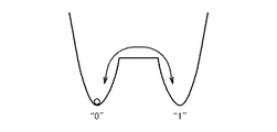
本願発明者は、次の点に着目した。図1及び図2で示された磁壁移動方式のMRAMにおいて、磁壁のダイナミクスは、下記数式(1)で表される。数式中、αは制動係数である。qは磁壁の位置である。Ψは、磁化の面内からの立ちあがり角である。Msは飽和磁化である。γはジャイロ磁気定数である。Δは磁壁幅である。εはピンポテンシャルである。Hkは異方性磁界である。uは電流密度である。βは非断熱係数である。 The inventor of the present application paid attention to the following points. In the domain wall motion type MRAM shown in FIGS. 1 and 2, the dynamics of the domain wall is expressed by the following formula (1). In the formula, α is a braking coefficient. q is the position of the domain wall. Ψ is a rising angle from the in-plane of magnetization. Ms is saturation magnetization. γ is a gyro magnetic constant. Δ is the domain wall width. ε is a pin potential. Hk is an anisotropic magnetic field. u is the current density. β is a non-adiabatic coefficient.

上記数式(1)によれば、磁壁はあたかもポテンシャル中の粒子のように振る舞う。図1の場合はくびれ部104、図2の場合は磁化固定領域111、112と磁化反転領域113との接続により大きさや形状は変わるが、ピンポテンシャルは、模式的には図3のようになる。スピン偏極した書き込み電流の印加により、磁壁はポテンシャルを上って行き、障壁を超えて遷移することができる。
According to Equation (1) above, the domain wall behaves as if it is a particle in the potential. In the case of FIG. 1, the size and shape change depending on the connection between the
しかしながら、書き込み電流がある程度以上に大きくなると、磁壁に大きなエネルギーが蓄えられる。そのため、書き込み電流が切断されたとき、図4に示されるように、磁壁が反動で元に戻ってしまう可能性がある。また、図5に示されるように、“0”状態から“1”状態への遷移に必要な方向と逆方向に書き込み電流が印加された場合を考える。その場合にも、磁壁に大きなエネルギーが蓄えられるため、磁壁が反動で“1”状態に遷移してしまう可能性がある。 However, when the write current becomes larger than a certain level, large energy is stored in the domain wall. For this reason, when the write current is cut off, the domain wall may return to its original state due to the reaction, as shown in FIG. Further, as shown in FIG. 5, consider a case where a write current is applied in the direction opposite to the direction necessary for transition from the “0” state to the “1” state. Even in this case, since a large amount of energy is stored in the domain wall, there is a possibility that the domain wall will transition to the “1” state by reaction.
このように、磁壁移動方式のMRAMでは、誤書き込みが発生する可能性があった。誤書き込みを抑制するためには、書き込み電流のマージンを狭くせざるを得ない。 As described above, in the domain wall motion type MRAM, erroneous writing may occur. In order to suppress erroneous writing, the write current margin must be narrowed.
本発明の目的は、磁壁移動方式のMRAMにおいて、書き込み電流のマージンを拡大させることができる技術を提供することにある。 An object of the present invention is to provide a technique capable of expanding a write current margin in a domain wall motion type MRAM.
本発明の一実施の形態によれば、磁壁移動方式のMRAMが提供される。そのMRAMは、強磁性層である磁気記録層と、非磁性層を介して磁気記録層に接続されたピン層とを備える。磁気記録層は、反転可能な磁化を有しピン層とオーバーラップする磁化反転領域と、磁化反転領域の第1境界に接続され磁化の向きが第1方向に固定された第1磁化固定領域と、磁化反転領域の第2境界に接続され磁化の向きが第2方向に固定された第2磁化固定領域と、を有する。第1方向及び第2方向は共に、磁化反転領域へ向かう方向、又は、磁化反転領域から離れる方向である。第1磁化固定領域と第2磁化固定領域との間を流れる電流により、磁化反転領域中を磁壁が移動する。第1磁化固定領域及び第2磁化固定領域の少なくとも一部分における制動係数が、磁化反転領域における制動係数よりも大きい。 According to an embodiment of the present invention, a domain wall motion type MRAM is provided. The MRAM includes a magnetic recording layer that is a ferromagnetic layer, and a pinned layer connected to the magnetic recording layer via a nonmagnetic layer. The magnetic recording layer includes a magnetization reversal region having reversible magnetization and overlapping with the pinned layer, a first magnetization fixed region connected to a first boundary of the magnetization reversal region and having a magnetization direction fixed in the first direction, And a second magnetization fixed region connected to the second boundary of the magnetization switching region and having the magnetization direction fixed in the second direction. Both the first direction and the second direction are directions toward the magnetization switching region or away from the magnetization switching region. The domain wall moves in the magnetization switching region by the current flowing between the first magnetization fixed region and the second magnetization fixed region. The braking coefficient in at least a part of the first magnetization fixed region and the second magnetization fixed region is larger than the braking coefficient in the magnetization switching region.
本発明の他の実施の形態によれば、磁壁移動方式のMRAMが提供される。そのMRAMは、強磁性層である磁気記録層と、非磁性層を介して磁気記録層に接続されたピン層とを備える。磁気記録層は、反転可能な磁化を有しピン層とオーバーラップする磁化反転領域と、磁化の向きが第1方向に固定された第1磁化固定領域と、磁化の向きが第2方向に固定された第2磁化固定領域と、磁化反転領域の第1境界と第1磁化固定領域との間に介在する第1制動領域と、磁化反転領域の第2境界と第2磁化固定領域との間に介在する第2制動領域と、を有する。第1方向及び第2方向は共に、磁化反転領域へ向かう方向、又は、磁化反転領域から離れる方向である。第1制動領域及び第2制動領域における制動係数は、磁化反転領域における制動係数よりも大きい。 According to another embodiment of the present invention, a domain wall motion type MRAM is provided. The MRAM includes a magnetic recording layer that is a ferromagnetic layer, and a pinned layer connected to the magnetic recording layer via a nonmagnetic layer. The magnetic recording layer has a magnetization reversal region that has reversible magnetization and overlaps the pinned layer, a first magnetization fixed region whose magnetization direction is fixed in the first direction, and a magnetization direction that is fixed in the second direction. Between the first magnetization fixed region, the first braking region interposed between the first boundary of the magnetization switching region and the first magnetization fixed region, and the second boundary of the magnetization switching region and the second magnetization fixed region And a second braking region interposed therebetween. Both the first direction and the second direction are directions toward the magnetization switching region or away from the magnetization switching region. The braking coefficient in the first braking area and the second braking area is larger than the braking coefficient in the magnetization switching area.
書き込み電流の印加により磁壁が第1磁化固定領域あるいは第2磁化固定領域に侵入した場合、制動係数の大きい部分で、急激にエネルギーの散逸が起こる。その結果、書き込み電流が切断された後、磁壁はポテンシャル障壁を超えることができなくなる。つまり、図4や図5で示されたような誤書き込みが起きにくくなる。従って、書き込み電流の設計自由度が向上し、書き込み電流のマージンを拡大させることが可能となる。 When the domain wall enters the first magnetization fixed region or the second magnetization fixed region by the application of the write current, energy dissipation occurs abruptly at a portion where the braking coefficient is large. As a result, the domain wall cannot exceed the potential barrier after the write current is cut. That is, erroneous writing as shown in FIGS. 4 and 5 is less likely to occur. Therefore, the design flexibility of the write current is improved, and the write current margin can be expanded.
本発明によれば、磁壁移動方式のMRAMにおいて、誤書き込みのリスクを低減することが可能となる。その結果、書き込み電流の設計自由度が向上し、書き込み電流のマージンを拡大させることが可能となる。 According to the present invention, it is possible to reduce the risk of erroneous writing in a domain wall motion type MRAM. As a result, the design flexibility of the write current is improved and the write current margin can be expanded.
添付図面を参照して、本発明の実施の形態に係るMRAMを説明する。本実施の形態に係るMRAMは、磁壁移動方式のMRAMである。 An MRAM according to an embodiment of the present invention will be described with reference to the accompanying drawings. The MRAM according to the present embodiment is a domain wall motion type MRAM.
1.磁気メモリセルの構造
1−1.基本構造
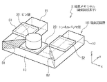
図6は、本実施の形態に係る磁気メモリセル1(磁気抵抗素子)の一例を示している。磁気メモリセル1は、強磁性体層である磁気記録層10とピン層30、及び非磁性体層であるトンネルバリヤ層20を備えている。トンネルバリヤ層20は、磁気記録層10とピン層30に挟まれており、これら磁気記録層10、トンネルバリヤ層20、及びピン層30によって磁気トンネル接合(MTJ)が形成されている。1. 1. Structure of magnetic memory cell 1-1. Basic Structure FIG. 6 shows an example of a magnetic memory cell 1 (magnetoresistive element) according to the present embodiment. The
磁気記録層10の材料としては、NiFe、NiFeにCu、Ta等を混ぜた合金、Ni、Fe、Coを含む合金、CoFeBを主成分とするアモルファス磁性体などが用いられる。トンネルバリヤ層20は、Al2O3膜やMgO膜等の薄い絶縁膜である。ピン層30の材料としては、CoFeやCoFeBなどが用いられる。As the material of the
ピン層30の磁化の向きは、図示されない反強磁性体層によって固定されている。一方、磁気記録層10は、反転可能な磁化を含んでおり、磁化自由層(フリー層)に相当する役割を果たす。
The magnetization direction of the pinned
図6に示されるように、本実施の形態に係る磁気記録層10は、第1磁化固定領域11、第2磁化固定領域12、及び磁化反転領域13を有している。磁化反転領域13は、X方向に延びるように形成されており、反転可能な磁化を有している。この磁化反転領域13は、ピン層30とオーバーラップするように形成されている。言い換えれば、磁気記録層10の磁化反転領域13の一部が、トンネルバリヤ層20を介してピン層30に接続されている。
As shown in FIG. 6, the
第1磁化固定領域11は、Y方向に延びるように形成されており、その磁化の向きは固定されている。同様に、第2磁化固定領域12は、Y方向に延びるように形成されており、その磁化の向きは固定されている。磁化固定領域11、12の磁化は、反強磁性体を隣接させることにより固定することもできる。尚、「磁化が固定されている」とは、書き込み動作の前後で磁化の方向が変わらないことを意味する。書き込み動作中に、磁化固定領域の一部の磁化の方向が変化しても、書き込み動作終了後には元に戻る。
The first magnetization fixed
これら磁化固定領域11、12、及び磁化反転領域13は、同一平面(XY面)上に形成されている。そのXY面における磁気記録層10の形状が、図7に示されている。図7に示されるように、磁化固定領域11、12、及び磁化反転領域13は、“U字状、又は、凹形状”に形成されている。具体的には、磁化固定領域11、12は、Y方向に沿って互いに略平行となるように形成されている。磁化反転領域13は、磁化固定領域11と12との間をつなぐように、X方向に沿って形成されている。第1磁化固定領域11と磁化反転領域13は、第1境界B1において互いに接触しており、第2磁化固定領域12と磁化反転領域13は、第2境界B2において互いに接触している。磁化反転領域13において、第1境界B1と第2境界B2は、対向するように位置している。また、第1磁化固定領域11の第1境界B1に対向する端部周辺には、電流供給端子15が設けられている。第2磁化固定領域12の第2境界B2に対向する端部周辺には、電流供給端子16が設けられている。
The magnetization fixed
図7には、各領域の磁化の向きも矢印によって示されている。更に、ピン層30の投影及びその磁化の向きも、点線及び点線矢印によって示されている。ピン層30の磁化の向きは、−X方向に固定されているとする。図7において、第1磁化固定領域11の磁化の向きは、+Y方向に固定されている。その向きは、第1境界B1から離れる(Away)方向である。また、第2磁化固定領域12の磁化の向きも、+Y方向に固定されている。その向きは、第2境界B2から離れる(Away)方向である。つまり、磁化固定領域11、12は共に、それらの磁化の向きが磁化反転領域13から離れるように形成されている。これは、磁化固定領域11、12の磁化の向きが、磁気記録層10の形状に沿って逆向きであることを意味する。
In FIG. 7, the direction of magnetization of each region is also indicated by arrows. Furthermore, the projection of the pinned
一方、磁化反転領域13の磁化の向きは反転可能であり、+X方向あるいは−X方向である。つまり、磁化反転領域13の磁化は、ピン層30の磁化と平行あるいは反平行になることが許される。磁化反転領域13の磁化の向きが+X方向の場合、すなわち、その磁化が第2境界B2へ向いている場合、第1磁化固定領域11が1つの磁区(magnetic domain)を形成し、磁化反転領域13と第2磁化固定領域12が別の磁区を形成する。つまり、第1境界B1に磁壁(domain wall)が形成される。一方、磁化反転領域13の磁化の向きが−X方向の場合、すなわち、その磁化が第1境界B1へ向いている場合、第1磁化固定領域11と磁化反転領域13が1つの磁区を形成し、第2磁化固定領域12が別の磁区を形成する。つまり、第2境界B2に磁壁が形成される。
On the other hand, the magnetization direction of the
このように、磁化反転領域13の磁化は、第1境界B1あるいは第2境界B2へ向き、磁気記録層10において、磁壁が第1境界B1あるいは第2境界B2に形成される。これは、磁化固定領域11、12の磁化の向きが、磁気記録層10の形状に沿って逆向きであることに起因する。
Thus, the magnetization of the
磁化固定領域11、12の磁化の向きは、図7で示された方向に限られない。上述のとおり、磁化固定領域11、12の磁化の向きは、磁気記録層10の形状に沿って逆向きであればよい。例えば図8において、第1磁化固定領域11の磁化の向きは、−Y方向に固定されている。その向きは、第1境界B1へ向かう(Toward)方向である。また、第2磁化固定領域12の磁化の向きも、−Y方向に固定されている。その向きは、第2境界B2へ向かう(Toward)方向である。つまり、磁化固定領域11、12の磁化は、共に磁化反転領域13へ向かう方向に固定されており、磁気記録層10の形状に沿って逆方向を向いている。
The magnetization directions of the magnetization fixed
1−2.制動領域
再度図6を参照して、本実施の形態に係る磁気メモリセル1は、更に、非磁性金属層51、52を備えている。非磁性金属層51は、磁気記録層10の第1磁化固定領域11の少なくとも一部に隣接して設けられている。非磁性金属層52は、磁気記録層10の第2磁化固定領域12の少なくとも一部に隣接して設けられている。非磁性金属層51、52は、磁化固定領域11、12に接触していてもよいし、Cu層やTa層を介して磁化固定領域11、12に接続されていてもよい。非磁性金属層51、52の材料としては、PtやPdが挙げられる。非磁性金属層51、52は、Pt、Pdの少なくともいずれかで形成されていればよい。1-2. Braking Area Referring again to FIG. 6, the
図7や図8において、非磁性金属層51、52に隣接している領域は、それぞれR1、R2で示されている。これら領域R1、R2は、以下、第1制動領域R1及び第2制動領域R2と参照される。第1制動領域R1は、第1磁化固定領域11に含まれており、第2制動領域R2は、第2磁化固定領域12に含まれている。本実施の形態に係る磁気記録層10は、磁化固定領域11、12、磁化反転領域13に加えて、制動領域R1、R2を有していると言える。
7 and 8, regions adjacent to the
上述の非磁性金属層51、52が隣接していることにより、制動領域R1、R2における制動係数αは、他の領域の制動係数αよりも大きくなる。特に、制動領域R1、R2における制動係数αは、磁化反転領域13の制動係数αよりも大きい。言い換えれば、磁化固定領域11、12の少なくとも一部分(R1,R2)における制動係数αが、磁化反転領域13における制動係数αよりも大きい。制動係数αは、スピンの歳差運動に対する制動の強さを示す。つまり、制動係数αは、磁壁移動に対する制動の強さを示す。制動係数αが大きい部分ではエネルギーの散逸が大きく、磁壁移動が抑制(制動)される。
Since the
尚、制動領域R1、R2を形成するための方法は、非磁性金属層51、52の設置だけに限られない。例えば、Pt、Pd、Bなどのイオンを磁化固定領域11、12に注入することにより、制動領域R1、R2を形成することも可能である。
The method for forming the braking regions R1 and R2 is not limited to the installation of the
2.磁壁移動
次に、磁気メモリセル1に対するデータの書き込み原理を説明する。データ書き込みは、スピン注入を利用した磁壁移動方式で行われる。書き込み電流は、MTJを貫通する方向ではなく、磁気記録層10内を平面的に流れる。その書き込み電流は、上記電流供給端子15、16から磁気記録層10に供給される。2. Next, the principle of writing data to the
図9は、図7で示された構造に対するデータの書き込み原理を示している。磁化反転領域13とピン層30の磁化の向きが平行である状態が、データ“0”に対応付けられている。データ“0”状態において、磁化反転領域13の磁化の向きは−X方向であり、磁壁DWは第2境界B2に存在する。一方、磁化反転領域13とピン層30の磁化の向きが反平行である状態が、データ“1”に対応付けられている。データ“1”状態において、磁化反転領域13の磁化の向きは+X方向であり、磁壁DWは第1境界B1に存在する。
FIG. 9 shows the data writing principle for the structure shown in FIG. A state in which the magnetization directions of the
データ“1”の書き込み時、第1書き込み電流IW1が、第1磁化固定領域11から磁化反転領域13を通って第2磁化固定領域12に流れる。この場合、磁化反転領域13には、第2磁化固定領域12からスピン電子が注入される。注入された電子のスピンは、磁化反転領域13の磁気モーメントに影響を及ぼす。その結果、磁化反転領域13の磁化の向きは、第2境界B2の方向へスイッチする。つまり、スピントランスファー効果により、磁化反転領域13の磁化が反転し、その磁化の向きが+X方向に変わる。
When data “1” is written, the first write current IW1 flows from the first magnetization fixed
一方、データ“0”の書き込み時、第2書き込み電流IW2が、第2磁化固定領域12から磁化反転領域13を通って第1磁化固定領域11に流れる。この場合、磁化反転領域13には、第1磁化固定領域11からスピン電子が注入される。その結果、磁化反転領域13の磁化が反転し、その磁化の向きが−X方向に変わる。このように、磁気記録層10内を平面的に流れる書き込み電流IW1,IW2によって、磁化反転領域13の磁化の方向がスイッチする。第1磁化固定領域11及び第2磁化固定領域12は、異なるスピンを有する電子の供給源の役割を果たしている。
On the other hand, when writing data “0”, the second write current IW 2 flows from the second magnetization fixed
上記書き込み動作は、「磁壁の移動(Domain Wall Motion)」という観点から述べることもできる。データ“1”の書き込み時、電子は、第2磁化固定領域12から第1磁化固定領域11の方へ移動する。この時、磁壁DWは、電子の移動方向と一致して、第2境界B2から第1境界B1の方へ移動する。一方、データ“0”の書き込み時、電子は、第1磁化固定領域11から第2磁化固定領域12の方へ移動する。この時、磁壁DWは、電子の移動方向と一致して、第1境界B1から第2境界B2の方へ移動する。つまり、磁気記録層10中の磁壁DWは、電子の移動方向に応じて磁化反転領域13中を行き来する。磁気メモリセル1は、磁壁DWの位置によってデータを記憶しているとも言える。
The write operation can also be described from the viewpoint of “domain wall motion”. When data “1” is written, electrons move from the second magnetization fixed
尚、データの読み出しに関しては、次の通りである。データ読み出し時、読み出し電流は、ピン層30と磁化反転領域13との間を流れるように供給される。例えば、読み出し電流は、磁化固定領域11、12のいずれかから、磁化反転領域13及びトンネルバリヤ層20を経由して、ピン層30へ流れる。あるいは、読み出し電流は、ピン層30から、トンネルバリヤ層20及び磁化反転領域13を経由して、磁化固定領域11、12のいずれかへ流れる。その読み出し電流あるいは読み出し電位に基づいて、磁気抵抗素子の抵抗値が検出され、磁化反転領域13の磁化の向きがセンスされる。
The data reading is as follows. When reading data, a read current is supplied so as to flow between the pinned
3.制動領域R1,R2の作用及び効果
本実施の形態における磁壁移動を更に詳細に説明することにより、制動領域R1、R2の作用及び効果を示す。3. Actions and Effects of Braking Areas R1 and R2 The actions and effects of the braking areas R1 and R2 will be described by further explaining the domain wall motion in the present embodiment.
図10は、本実施の形態における磁壁移動の一例を模式的に示している。図10中、状態(a)は、初期状態を表している。初期状態は、データ“0”状態であり、磁壁DWは第2境界B2に存在している。データ“0”状態からデータ“1”状態への遷移時には、上述の通り、第1書き込み電流IW1が流される。これにより、磁壁DWが、磁化反転領域13を通って第1磁化固定領域11の方へ移動する(状態(b)、(c))。
FIG. 10 schematically shows an example of domain wall motion in the present embodiment. In FIG. 10, a state (a) represents an initial state. The initial state is a data “0” state, and the domain wall DW exists at the second boundary B2. At the time of transition from the data “0” state to the data “1” state, the first write current IW1 flows as described above. As a result, the domain wall DW moves toward the first magnetization fixed
更に、磁壁DWは、第1境界B1を超えて、第1磁化固定領域11に侵入する。第1磁化固定領域11中には第1制動領域R1が存在する。状態(d)に示されるように、磁壁DWが第1制動領域R1に侵入すると、エネルギーの散逸が激しく起こる。これにより、磁壁DWの運動量は失われる。第1書き込み電流IW1の供給が停止すると、磁壁DWは減衰振動しながら第1境界B1に落ち着く(状態(e))。図3の模式図で言えば、第1境界B1は、ポテンシャルの底に相当しており、磁壁DWが最も安定化する位置である。磁壁DWが第1境界B1に落ち着いた状態(e)が、データ“1”状態である。
Further, the domain wall DW enters the first magnetization fixed
このように、磁壁DWは、第1境界B1を超えたとしても、第1制動領域R1において運動量を失う。その結果、第1書き込み電流IW1が切断された後、磁壁DWはポテンシャル障壁を超えることができなくなる。つまり、磁壁DWが反動で初期状態に戻ること(図4参照)が防止される。すなわち、誤書き込みが防止される。 Thus, even if the domain wall DW exceeds the first boundary B1, the momentum is lost in the first braking region R1. As a result, after the first write current IW1 is cut, the domain wall DW cannot exceed the potential barrier. That is, the domain wall DW is prevented from returning to the initial state due to the reaction (see FIG. 4). That is, erroneous writing is prevented.
図11は、磁壁移動の他の例を模式的に示している。図11中、状態(a)は、初期状態を表している。初期状態は、データ“1”状態であり、磁壁DWは第1境界B1に存在している。このデータ“1”状態から、更に、データ“1”書き込みのための第1書き込み電流IW1が流される場合を考える。 FIG. 11 schematically shows another example of domain wall motion. In FIG. 11, the state (a) represents the initial state. The initial state is the data “1” state, and the domain wall DW exists at the first boundary B1. Consider a case where a first write current IW1 for writing data “1” is further supplied from this data “1” state.
この時、磁壁DWは、第1境界B1から第1磁化固定領域11の方へ侵入する。状態(b)に示されるように、磁壁DWが第1制動領域R1に侵入すると、エネルギーの散逸が激しく起こり、磁壁DWの運動量は失われる。従って、第1書き込み電流IW1の供給が停止した際、図10の場合と同様に、磁壁DWは、ポテンシャル障壁を超えることなく第1境界B1に落ち着く(状態(c))。つまり、書き込み動作後もデータ“1”状態が維持される。すなわち、誤書込みが防止される。
At this time, the domain wall DW enters the first magnetization fixed
一般的に、書き込み動作前の状態が“0”状態、“1”状態のどちらであるかは分からない。そのため、書き込み前に予備読み出し動作を実行し、その読み出し結果に応じて書き込み動作を行うことが考えられる。しかしその場合、予備読み出し動作の分だけ全体としての書き込み時間が遅くなる。動作速度の観点からは、予備読み出し動作を実施することなく書き込み動作を実行することが好ましい。但しその場合、図11で示されたように、データ“1”のセルに対してデータ“1”の書き込み動作が行われる可能性がある。従来技術では、反動により誤書き込みが行われる可能性があった(図5参照)。しかしながら、本実施の形態によれば、図11で示されたようにそのような誤書き込みが防止される。すなわち、書き込み前の状態に依存せず、意図したデータ状態が得られる。 Generally, it is not known whether the state before the write operation is the “0” state or the “1” state. Therefore, it is conceivable to perform a preliminary read operation before writing and perform a write operation according to the read result. However, in that case, the entire writing time is delayed by the amount of the preliminary reading operation. From the viewpoint of operation speed, it is preferable to perform the write operation without performing the preliminary read operation. In this case, however, as shown in FIG. 11, the data “1” write operation may be performed on the data “1” cell. In the prior art, there was a possibility of erroneous writing due to reaction (see FIG. 5). However, according to the present embodiment, such erroneous writing is prevented as shown in FIG. That is, the intended data state can be obtained without depending on the state before writing.
以上に説明されたように、制動係数αが高い制動領域R1、R2により、磁壁DWは運動量を失う。磁壁DWが磁化固定領域11、12に侵入したとしても、制動領域R1、R2で急激にエネルギーの散逸が起こる。その結果、書き込み電流が切断された後に、磁壁DWはポテンシャル障壁を超えることができなくなる。つまり、図4や図5で示されたような誤書き込みのリスクが低減される。従って、書き込み電流の設計自由度が向上し、書き込み電流のマージンを拡大させることが可能となる。
As described above, the domain wall DW loses momentum due to the braking regions R1 and R2 having a high braking coefficient α. Even if the domain wall DW enters the magnetization fixed
磁壁DWのエネルギーを早い段階で散逸させるためには、制動領域R1、R2を境界B1、B2の近傍に設けることが望ましい。好適には、第1制動領域R1は第1境界B1に接するように設けられ、第2制動領域R2は第2境界B2に接するように設けられる。これにより、磁壁DWのエネルギーを効率的に散逸させることが可能となる。 In order to dissipate the energy of the domain wall DW at an early stage, it is desirable to provide the braking regions R1 and R2 in the vicinity of the boundaries B1 and B2. Preferably, the first braking region R1 is provided in contact with the first boundary B1, and the second braking region R2 is provided in contact with the second boundary B2. Thereby, the energy of the domain wall DW can be efficiently dissipated.
更に、本実施の形態によれば、制動領域R1、R2における制動係数αは、磁化反転領域13の制動係数αよりも大きい。言い換えれば、磁化反転領域13における制動係数αは、相対的に小さい値に設定されている。データの遷移は、磁化固定領域11、12間の磁化反転領域13における磁壁DWの移動により起こる。本実施の形態では、磁化反転領域13での磁壁DWに対する制動力は弱いため、データの遷移自体は起こりやすい。従って、磁化反転に要する書き込み電流IW1、IW2が増大することはない。また、磁化反転に要する時間が増大することもない。
Furthermore, according to the present embodiment, the braking coefficient α in the braking regions R1 and R2 is larger than the braking coefficient α in the
また、制動領域R1、R2は、磁壁DWが磁化固定領域11、12を突き抜けて消失してしまうことも防止する。
The braking regions R1 and R2 also prevent the domain wall DW from penetrating through the magnetization fixed
4.変形例
図12は、磁気記録層10の変形例を示している。図12において、第1制動領域R1は、第1磁化固定領域11と磁化反転領域13の第1境界B1との間に介在している。つまり、第1制動領域R1は、第1磁化固定領域11から独立して設けられている。第1磁化固定領域11は、第1制動領域R1を介して磁化反転領域13に接続されている。また、第2制動領域R2は、第2磁化固定領域12と磁化反転領域13の第2境界B2との間に介在している。つまり、第2制動領域R2は、第2磁化固定領域12から独立して設けられている。第2磁化固定領域12は、第2制動領域R2を介して磁化反転領域13に接続されている。このような構造でも同じ効果が得られる。4). Modification FIG. 12 shows a modification of the
図13は、磁気記録層10の他の変形例を示している。図13において、磁化固定領域11、12、及び磁化反転領域13は、“直線状”に形成されている。つまり、磁化固定領域11、12は、X方向に沿って互いに略平行となるように形成されている。磁化反転領域13は、磁化固定領域11、12との間をつなぐように、X方向に沿って形成されている。第1磁化固定領域11の磁化の向きは−X方向に固定され、第2磁化固定領域12の磁化の向きは+X方向に固定されている。つまり、磁化固定領域11、12の磁化は、共に磁化反転領域13から離れる方向(Away)に固定されており、逆方向を向いている。第1制動領域R1は、第1磁化固定領域11の少なくとも一部に形成されている。第2制動領域R2は、第2磁化固定領域12の少なくとも一部に形成されている。このような構造でも同じ効果が得られる。尚、磁気記録層10の側部にはノッチ14が設けられており、境界B1、B2の面積が他の部分よりも小さくなっている。これにより、磁壁DWを安定的に留めることが可能となる。尚、磁化固定領域11、12の磁化は、図13の場合と逆向きに固定されていてもよい。
FIG. 13 shows another modification of the
図14は、磁気記録層10の更に他の変形例を示している。図14において、磁化固定領域11、12、磁化反転領域13、及び制動領域R1、R2が、“直線状”に形成されている。第1制動領域R1は、第1磁化固定領域11と磁化反転領域13の第1境界B1との間に介在している。第1磁化固定領域11は、第1制動領域R1を介して磁化反転領域13に接続されている。また、第2制動領域R2は、第2磁化固定領域12と磁化反転領域13の第2境界B2との間に介在している。第2磁化固定領域12は、第2制動領域R2を介して磁化反転領域13に接続されている。このような構造でも同じ効果が得られる。
FIG. 14 shows still another modification of the
5.MRAMの構成
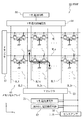
図15は、本実施の形態に係るMRAMの構成の一例を示している。図15において、MRAM60は、複数の磁気メモリセル1がマトリックス状に配置されたメモリセルアレイ61を有している。このメモリセルアレイ61は、データの記録に用いられる磁気メモリセル1と共に、データ読み出しの際に参照されるリファレンスセル1rを含んでいる。リファレンスセル1rの構造は、磁気メモリセル1と同じである。5. Configuration of MRAM FIG. 15 shows an example of the configuration of the MRAM according to the present embodiment. In FIG. 15, an
各磁気メモリセル1は、図6に示された磁気抵抗素子に加え、選択トランジスタTR1、TR2を有している。選択トランジスタTR1のソース/ドレインの一方は、第1磁化固定領域11の電流供給端子15に接続され、他方は第1ビット線BL1に接続されている。選択トランジスタTR2のソース/ドレインの一方は、第2磁化固定領域12の電流供給端子16に接続され、他方は第2ビット線BL2に接続されている。選択トランジスタTR1、TR2のゲートはワード線WLに接続されている。磁気抵抗素子のピン層30は、電極を介してグランド線に接続されている。
Each
ワード線WLは、Xセレクタ62に接続されている。Xセレクタ62は、データの書き込み・読み出しにおいて、対象メモリセル1sにつながるワード線WLを選択ワード線WLsとして選択する。第1ビット線BL1はY側電流終端回路64に接続されており、第2ビット線BL2はYセレクタ63に接続されている。Yセレクタ63は、対象メモリセル1sにつながる第2ビット線BL2を選択第2ビット線BL2sとして選択する。Y側電流終端回路64は、対象メモリセル1sにつながる第1ビット線BL1を選択第1ビット線BL1sとして選択する。
The word line WL is connected to the X selector 62. The X selector 62 selects a word line WL connected to the
Y側電流源回路65は、データ書き込み時、選択第2ビット線BL2sに対し、所定の書き込み電流(IW1,IW2)の供給又は引き込みを行う。Y側電源回路66は、データ書き込み時、Y側電流終端回路64に所定の電圧を供給する。その結果、書き込み電流(IW1,IW2)は、Yセレクタ63へ流れ込む、あるいは、Yセレクタ63から流れ出す。これらXセレクタ62、Yセレクタ63、Y側電流終端回路64、Y側電流源回路65、及びY側電源回路66は、磁気メモリセル1に書き込み電流IW1,IW2を供給するための「書き込み電流供給回路」を構成している。
The Y-side
データ読み出し時、第1ビット線BL1は“Open”に設定される。読み出し電流負荷回路67は、選択第2ビット線BL2sに所定の読み出し電流を流す。また、読み出し電流負荷回路67は、リファレンスセル1rにつながるリファレンス第2ビット線BL2rに所定の電流を流す。センスアンプ68は、リファレンス第2ビット線BL2rの電位と選択第2ビット線BL2sの電位の差に基づいて、対象メモリセル1sからデータを読み出し、そのデータを出力する。
When reading data, the first bit line BL1 is set to “Open”. The read
以上、本発明の実施の形態が添付の図面を参照することにより説明された。但し、本発明は、上述の実施の形態に限定されず、要旨を逸脱しない範囲で当業者により適宜変更され得る。 The embodiments of the present invention have been described above with reference to the accompanying drawings. However, the present invention is not limited to the above-described embodiments, and can be appropriately changed by those skilled in the art without departing from the scope of the invention.
Claims (7)
強磁性層である磁気記録層と、
非磁性層を介して前記磁気記録層に接続されたピン層と
を具備し、
前記磁気記録層は、
反転可能な磁化を有し前記ピン層とオーバーラップする磁化反転領域と、
前記磁化反転領域の第1境界に接続され、磁化の向きが第1方向に固定された第1磁化固定領域と、
前記磁化反転領域の第2境界に接続され、磁化の向きが第2方向に固定された第2磁化固定領域と
を有し、
前記第1方向及び前記第2方向は共に、前記磁化反転領域へ向かう方向、又は、前記磁化反転領域から離れる方向であり、
スピンの歳差運動に対する制動の強さが制動係数で表されるとき、
前記第1磁化固定領域及び前記第2磁化固定領域の少なくとも一部分における前記制動係数は、前記磁化反転領域における前記制動係数よりも大きく、
前記少なくとも一部分には、Pt、Pd、Bからなる群から選ばれた少なくとも1つのイオンが注入されている
磁気ランダムアクセスメモリ。A magnetic random access memory of a domain wall motion system,
A magnetic recording layer which is a ferromagnetic layer;
A pinned layer connected to the magnetic recording layer via a nonmagnetic layer,
The magnetic recording layer is
A magnetization reversal region having a reversible magnetization and overlapping the pinned layer;
A first magnetization fixed region connected to a first boundary of the magnetization switching region and having a magnetization direction fixed in a first direction;
A second magnetization fixed region connected to a second boundary of the magnetization switching region and having a magnetization direction fixed in a second direction;
The first direction and the second direction are both directions toward the magnetization switching region or away from the magnetization switching region,
When the strength of braking against spin precession is expressed as a braking coefficient,
The damping coefficient of at least a portion of the first magnetization fixed region and said second magnetization fixed region is much larger than the damping coefficient in the magnetization inversion region,
A magnetic random access memory in which at least one ion selected from the group consisting of Pt, Pd, and B is implanted in the at least part .
前記少なくとも一部分は、前記第1境界及び前記第2境界に接している
磁気ランダムアクセスメモリ。A magnetic random access memory according to claim 1,
The at least part of the magnetic random access memory is in contact with the first boundary and the second boundary.
前記第1磁化固定領域と前記第2磁化固定領域は、互いに略平行となるように形成され、
前記磁化反転領域は、前記第1磁化固定領域と前記第2磁化固定領域との間をつなぐように形成された
磁気ランダムアクセスメモリ。A magnetic random access memory according to claim 1 or 2,
The first magnetization fixed region and the second magnetization fixed region are formed to be substantially parallel to each other,
The magnetic random access memory, wherein the magnetization switching region is formed to connect between the first magnetization fixed region and the second magnetization fixed region.
前記第1磁化固定領域及び前記第2磁化固定領域は、前記第1方向と前記第2方向が同じになるように形成された
磁気ランダムアクセスメモリ。The magnetic random access memory according to claim 3 ,
The magnetic random access memory, wherein the first magnetization fixed region and the second magnetization fixed region are formed so that the first direction and the second direction are the same.
前記磁化反転領域、前記第1磁化固定領域、及び前記第2磁化固定領域は、同一平面上に直線状に形成され、
前記第1方向と前記第2方向は逆方向である
磁気ランダムアクセスメモリ。The magnetic random access memory according to claim 3 ,
The magnetization switching region, the first magnetization fixed region, and the second magnetization fixed region are linearly formed on the same plane,
The magnetic random access memory, wherein the first direction and the second direction are opposite directions.
前記第1磁化固定領域と前記第2磁化固定領域との間を流れる電流により、磁壁が前記磁化反転領域中を移動する
磁気ランダムアクセスメモリ。A magnetic random access memory according to any one of claims 1 to 5,
A magnetic random access memory in which a domain wall moves in the magnetization switching region by a current flowing between the first magnetization fixed region and the second magnetization fixed region.
強磁性層である磁気記録層と、
非磁性層を介して前記磁気記録層に接続されたピン層と
を具備し、
前記磁気記録層は、
反転可能な磁化を有し前記ピン層とオーバーラップする磁化反転領域と、
磁化の向きが第1方向に固定された第1磁化固定領域と、
磁化の向きが第2方向に固定された第2磁化固定領域と、
前記磁化反転領域の第1境界と前記第1磁化固定領域との間に介在する第1制動領域と、
前記磁化反転領域の第2境界と前記第2磁化固定領域との間に介在する第2制動領域と
を有し、
前記第1方向及び前記第2方向は共に、前記磁化反転領域へ向かう方向、又は、前記磁化反転領域から離れる方向であり、
スピンの歳差運動に対する制動の強さが制動係数で表されるとき、
前記第1制動領域及び前記第2制動領域における前記制動係数は、前記磁化反転領域における前記制動係数よりも大きい
磁気ランダムアクセスメモリ。A magnetic random access memory of a domain wall motion system,
A magnetic recording layer which is a ferromagnetic layer;
A pinned layer connected to the magnetic recording layer via a nonmagnetic layer,
The magnetic recording layer is
A magnetization reversal region having a reversible magnetization and overlapping the pinned layer;
A first magnetization fixed region in which the magnetization direction is fixed in the first direction;
A second magnetization fixed region in which the magnetization direction is fixed in the second direction;
A first braking region interposed between the first boundary of the magnetization switching region and the first magnetization fixed region;
A second braking region interposed between the second boundary of the magnetization switching region and the second magnetization fixed region;
The first direction and the second direction are both directions toward the magnetization switching region or away from the magnetization switching region,
When the strength of braking against spin precession is expressed as a braking coefficient,
The magnetic random access memory, wherein the braking coefficient in the first braking area and the second braking area is larger than the braking coefficient in the magnetization switching area.
Priority Applications (1)
| Application Number | Priority Date | Filing Date | Title |
|---|---|---|---|
| JP2009502473A JP5201538B2 (en) | 2007-03-07 | 2008-01-15 | Magnetic random access memory |
Applications Claiming Priority (4)
| Application Number | Priority Date | Filing Date | Title |
|---|---|---|---|
| JP2007056693 | 2007-03-07 | ||
| JP2007056693 | 2007-03-07 | ||
| PCT/JP2008/050344 WO2008108108A1 (en) | 2007-03-07 | 2008-01-15 | Magnetic random access memory |
| JP2009502473A JP5201538B2 (en) | 2007-03-07 | 2008-01-15 | Magnetic random access memory |
Publications (2)
| Publication Number | Publication Date |
|---|---|
| JPWO2008108108A1 JPWO2008108108A1 (en) | 2010-06-10 |
| JP5201538B2 true JP5201538B2 (en) | 2013-06-05 |
Family
ID=39738004
Family Applications (1)
| Application Number | Title | Priority Date | Filing Date |
|---|---|---|---|
| JP2009502473A Active JP5201538B2 (en) | 2007-03-07 | 2008-01-15 | Magnetic random access memory |
Country Status (3)
| Country | Link |
|---|---|
| US (1) | US8238135B2 (en) |
| JP (1) | JP5201538B2 (en) |
| WO (1) | WO2008108108A1 (en) |
Families Citing this family (5)
| Publication number | Priority date | Publication date | Assignee | Title |
|---|---|---|---|---|
| WO2010074130A1 (en) | 2008-12-25 | 2010-07-01 | 日本電気株式会社 | Magnetic memory element and magnetic random access memory |
| WO2010074132A1 (en) * | 2008-12-25 | 2010-07-01 | 日本電気株式会社 | Magnetic memory element and magnetic random access memory |
| US8576519B1 (en) * | 2012-10-11 | 2013-11-05 | HGST Netherlands B.V. | Current-perpendicular-to-the-plane (CPP) magnetoresistive (MR) sensor with magnetic damping material at the sensor edges |
| CN105096963B (en) * | 2014-04-25 | 2018-06-26 | 华为技术有限公司 | Write device and magnetic storage |
| US10755759B2 (en) | 2018-06-28 | 2020-08-25 | International Business Machines Corporation | Symmetrically programmable resistive synapse for RPU using current-programmed single domain wall ferroelectric |
Citations (3)
| Publication number | Priority date | Publication date | Assignee | Title |
|---|---|---|---|---|
| JP2005150482A (en) * | 2003-11-18 | 2005-06-09 | Sony Corp | Magnetoresistance effect element and magnetic memory device |
| JP2005191032A (en) * | 2003-12-24 | 2005-07-14 | Toshiba Corp | Magnetic storage device and method of writing magnetic information |
| WO2007020823A1 (en) * | 2005-08-15 | 2007-02-22 | Nec Corporation | Magnetic memory cell, magnetic random access memory and method for reading/writing data in magnetic random access memory |
Family Cites Families (17)
| Publication number | Priority date | Publication date | Assignee | Title |
|---|---|---|---|---|
| US6767655B2 (en) * | 2000-08-21 | 2004-07-27 | Matsushita Electric Industrial Co., Ltd. | Magneto-resistive element |
| JP4666774B2 (en) | 2001-01-11 | 2011-04-06 | キヤノン株式会社 | Magnetic thin film memory element, magnetic thin film memory, and information recording / reproducing method |
| US6834005B1 (en) | 2003-06-10 | 2004-12-21 | International Business Machines Corporation | Shiftable magnetic shift register and method of using the same |
| JP2005093488A (en) | 2003-09-12 | 2005-04-07 | Sony Corp | Magnetoresistive effect element, its manufacturing method, magnetic memory device, and its manufacturing method |
| JP4143020B2 (en) | 2003-11-13 | 2008-09-03 | 株式会社東芝 | Magnetoresistive element and magnetic memory |
| JP2005223086A (en) * | 2004-02-04 | 2005-08-18 | Sony Corp | Magnetic storage element, driving method therefor, and magnetic memory |
| JP2006073930A (en) | 2004-09-06 | 2006-03-16 | Canon Inc | Varying method of magnetizing state of magnetoresistance effect element using magnetic wall movement, magnetic memory device using the method, and solid magnetic memory |
| JP4920881B2 (en) | 2004-09-27 | 2012-04-18 | 株式会社日立製作所 | Low power consumption magnetic memory and magnetization information writing device |
| JP2006303159A (en) * | 2005-04-20 | 2006-11-02 | Fuji Electric Holdings Co Ltd | Spin injection magnetic domain moving element and device using this |
| JP4444241B2 (en) * | 2005-10-19 | 2010-03-31 | 株式会社東芝 | Magnetoresistive element, magnetic random access memory, electronic card and electronic device |
| KR100763910B1 (en) * | 2006-02-23 | 2007-10-05 | 삼성전자주식회사 | Magnetic memory device using magnetic domain dragging |
| KR100923302B1 (en) * | 2006-02-27 | 2009-10-27 | 삼성전자주식회사 | A magnetic memory element |
| JP5077732B2 (en) | 2006-03-23 | 2012-11-21 | 日本電気株式会社 | Magnetic memory cell, magnetic random access memory, semiconductor device, and manufacturing method of semiconductor device |
| JP2007317895A (en) | 2006-05-26 | 2007-12-06 | Fujitsu Ltd | Magnetoresistive memory device |
| JP4969981B2 (en) * | 2006-10-03 | 2012-07-04 | 株式会社東芝 | Magnetic storage |
| US7936627B2 (en) * | 2006-12-12 | 2011-05-03 | Nec Corporation | Magnetoresistance effect element and MRAM |
| WO2008099626A1 (en) * | 2007-02-13 | 2008-08-21 | Nec Corporation | Magnetoresistance effect element and magnetic random access memory |
-
2008
- 2008-01-15 US US12/529,387 patent/US8238135B2/en not_active Expired - Fee Related
- 2008-01-15 JP JP2009502473A patent/JP5201538B2/en active Active
- 2008-01-15 WO PCT/JP2008/050344 patent/WO2008108108A1/en active Application Filing
Patent Citations (3)
| Publication number | Priority date | Publication date | Assignee | Title |
|---|---|---|---|---|
| JP2005150482A (en) * | 2003-11-18 | 2005-06-09 | Sony Corp | Magnetoresistance effect element and magnetic memory device |
| JP2005191032A (en) * | 2003-12-24 | 2005-07-14 | Toshiba Corp | Magnetic storage device and method of writing magnetic information |
| WO2007020823A1 (en) * | 2005-08-15 | 2007-02-22 | Nec Corporation | Magnetic memory cell, magnetic random access memory and method for reading/writing data in magnetic random access memory |
Also Published As
| Publication number | Publication date |
|---|---|
| US8238135B2 (en) | 2012-08-07 |
| JPWO2008108108A1 (en) | 2010-06-10 |
| US20100096715A1 (en) | 2010-04-22 |
| WO2008108108A1 (en) | 2008-09-12 |
Similar Documents
| Publication | Publication Date | Title |
|---|---|---|
| JP5206414B2 (en) | Magnetic memory cell and magnetic random access memory | |
| US10672446B2 (en) | Exchange bias utilization type magnetization rotational element, exchange bias utilization type magnetoresistance effect element, exchange bias utilization type magnetic memory, non-volatile logic circuit, and magnetic neuron element | |
| US8040724B2 (en) | Magnetic domain wall random access memory | |
| JP5062481B2 (en) | Magnetic memory cell, magnetic random access memory, and data read / write method to magnetic random access memory | |
| JP5441005B2 (en) | Domain wall moving element and magnetic random access memory | |
| JP5366014B2 (en) | Magnetic random access memory and initialization method thereof | |
| EP1826774B1 (en) | Magnetic memory device using magnetic domain motion | |
| US8514616B2 (en) | Magnetic memory element and magnetic memory | |
| JP5201539B2 (en) | Magnetic random access memory | |
| JP5299735B2 (en) | Domain wall random access memory | |
| JP5545213B2 (en) | Magnetic random access memory and initialization method thereof | |
| JP5257831B2 (en) | Magnetic random access memory and initialization method thereof | |
| JPWO2007119446A1 (en) | MRAM and data read / write method of MRAM | |
| JP5360600B2 (en) | Magnetic random access memory and initialization method of magnetic random access memory | |
| JP5201538B2 (en) | Magnetic random access memory | |
| JPWO2009019948A1 (en) | Magnetic recording apparatus and magnetization fixing method | |
| JP5754531B2 (en) | Magnetoresistive element and method of manufacturing magnetic random access memory | |
| JP5382295B2 (en) | Magnetic random access memory | |
| WO2011118461A1 (en) | Magnetic memory |
Legal Events
| Date | Code | Title | Description |
|---|---|---|---|
| A621 | Written request for application examination |
Free format text: JAPANESE INTERMEDIATE CODE: A621 Effective date: 20101203 |
|
| A131 | Notification of reasons for refusal |
Free format text: JAPANESE INTERMEDIATE CODE: A131 Effective date: 20121102 |
|
| A521 | Request for written amendment filed |
Free format text: JAPANESE INTERMEDIATE CODE: A523 Effective date: 20121219 |
|
| TRDD | Decision of grant or rejection written | ||
| A01 | Written decision to grant a patent or to grant a registration (utility model) |
Free format text: JAPANESE INTERMEDIATE CODE: A01 Effective date: 20130121 |
|
| R150 | Certificate of patent or registration of utility model |
Ref document number: 5201538 Country of ref document: JP Free format text: JAPANESE INTERMEDIATE CODE: R150 Free format text: JAPANESE INTERMEDIATE CODE: R150 |
|
| A61 | First payment of annual fees (during grant procedure) |
Free format text: JAPANESE INTERMEDIATE CODE: A61 Effective date: 20130203 |
|
| FPAY | Renewal fee payment (event date is renewal date of database) |
Free format text: PAYMENT UNTIL: 20160222 Year of fee payment: 3 |