JP5198449B2 - How to reduce noise in digital images - Google Patents
How to reduce noise in digital images Download PDFInfo
- Publication number
- JP5198449B2 JP5198449B2 JP2009523947A JP2009523947A JP5198449B2 JP 5198449 B2 JP5198449 B2 JP 5198449B2 JP 2009523947 A JP2009523947 A JP 2009523947A JP 2009523947 A JP2009523947 A JP 2009523947A JP 5198449 B2 JP5198449 B2 JP 5198449B2
- Authority
- JP
- Japan
- Prior art keywords
- digital image
- image
- noise
- dark current
- sensor
- Prior art date
- Legal status (The legal status is an assumption and is not a legal conclusion. Google has not performed a legal analysis and makes no representation as to the accuracy of the status listed.)
- Expired - Fee Related
Links
- 238000000034 method Methods 0.000 claims description 46
- 230000000694 effects Effects 0.000 claims description 5
- 230000003902 lesion Effects 0.000 claims description 5
- 230000003211 malignant effect Effects 0.000 claims description 3
- 230000003595 spectral effect Effects 0.000 claims description 3
- 230000008569 process Effects 0.000 description 15
- 238000012545 processing Methods 0.000 description 7
- 230000009467 reduction Effects 0.000 description 7
- 238000004458 analytical method Methods 0.000 description 6
- 238000007619 statistical method Methods 0.000 description 5
- 230000003287 optical effect Effects 0.000 description 4
- 230000008859 change Effects 0.000 description 3
- 238000011156 evaluation Methods 0.000 description 3
- 238000003384 imaging method Methods 0.000 description 3
- PHEDXBVPIONUQT-RGYGYFBISA-N phorbol 13-acetate 12-myristate Chemical compound C([C@]1(O)C(=O)C(C)=C[C@H]1[C@@]1(O)[C@H](C)[C@H]2OC(=O)CCCCCCCCCCCCC)C(CO)=C[C@H]1[C@H]1[C@]2(OC(C)=O)C1(C)C PHEDXBVPIONUQT-RGYGYFBISA-N 0.000 description 3
- 230000000875 corresponding effect Effects 0.000 description 2
- 201000001441 melanoma Diseases 0.000 description 2
- 238000012986 modification Methods 0.000 description 2
- 230000004048 modification Effects 0.000 description 2
- 238000012887 quadratic function Methods 0.000 description 2
- 230000004044 response Effects 0.000 description 2
- 238000012935 Averaging Methods 0.000 description 1
- 238000003491 array Methods 0.000 description 1
- 238000004364 calculation method Methods 0.000 description 1
- 238000012937 correction Methods 0.000 description 1
- 230000002596 correlated effect Effects 0.000 description 1
- 208000035250 cutaneous malignant susceptibility to 1 melanoma Diseases 0.000 description 1
- 238000001514 detection method Methods 0.000 description 1
- 238000003745 diagnosis Methods 0.000 description 1
- 238000010586 diagram Methods 0.000 description 1
- 238000005286 illumination Methods 0.000 description 1
- 238000005259 measurement Methods 0.000 description 1
- 238000004445 quantitative analysis Methods 0.000 description 1
- 238000011946 reduction process Methods 0.000 description 1
- 238000002310 reflectometry Methods 0.000 description 1
- 230000002123 temporal effect Effects 0.000 description 1
- 238000002604 ultrasonography Methods 0.000 description 1
- 238000012795 verification Methods 0.000 description 1
Images


Classifications
-
- H—ELECTRICITY
- H04—ELECTRIC COMMUNICATION TECHNIQUE
- H04N—PICTORIAL COMMUNICATION, e.g. TELEVISION
- H04N5/00—Details of television systems
- H04N5/14—Picture signal circuitry for video frequency region
- H04N5/21—Circuitry for suppressing or minimising disturbance, e.g. moiré or halo
-
- G06T5/70—
-
- H—ELECTRICITY
- H04—ELECTRIC COMMUNICATION TECHNIQUE
- H04N—PICTORIAL COMMUNICATION, e.g. TELEVISION
- H04N25/00—Circuitry of solid-state image sensors [SSIS]; Control thereof
- H04N25/60—Noise processing, e.g. detecting, correcting, reducing or removing noise
- H04N25/63—Noise processing, e.g. detecting, correcting, reducing or removing noise applied to dark current
-
- H—ELECTRICITY
- H04—ELECTRIC COMMUNICATION TECHNIQUE
- H04N—PICTORIAL COMMUNICATION, e.g. TELEVISION
- H04N25/00—Circuitry of solid-state image sensors [SSIS]; Control thereof
- H04N25/60—Noise processing, e.g. detecting, correcting, reducing or removing noise
- H04N25/67—Noise processing, e.g. detecting, correcting, reducing or removing noise applied to fixed-pattern noise, e.g. non-uniformity of response
- H04N25/671—Noise processing, e.g. detecting, correcting, reducing or removing noise applied to fixed-pattern noise, e.g. non-uniformity of response for non-uniformity detection or correction
- H04N25/677—Noise processing, e.g. detecting, correcting, reducing or removing noise applied to fixed-pattern noise, e.g. non-uniformity of response for non-uniformity detection or correction for reducing the column or line fixed pattern noise
-
- G—PHYSICS
- G06—COMPUTING; CALCULATING OR COUNTING
- G06T—IMAGE DATA PROCESSING OR GENERATION, IN GENERAL
- G06T2207/00—Indexing scheme for image analysis or image enhancement
- G06T2207/20—Special algorithmic details
- G06T2207/20004—Adaptive image processing
- G06T2207/20008—Globally adaptive
-
- G—PHYSICS
- G06—COMPUTING; CALCULATING OR COUNTING
- G06T—IMAGE DATA PROCESSING OR GENERATION, IN GENERAL
- G06T2207/00—Indexing scheme for image analysis or image enhancement
- G06T2207/20—Special algorithmic details
- G06T2207/20076—Probabilistic image processing
Description
本明細書は、デジタル画像のノイズを低減する方法に関する。 The present specification relates to a method for reducing noise in a digital image.
CMOS画像センサによって生成されるデジタル画像などのデジタル画像に現れる特徴が(例えば、医学的応用においてなど)量的に分析されることになっているとき、分析の前に画像からノイズを低減するかまたは除去することは有用である。デジタル画像を生成する信号がノイズと比べて低い場合に、画像からノイズを低減するかまたは除去することは同様に有用である。 When features that appear in a digital image, such as a digital image generated by a CMOS image sensor, are to be quantitatively analyzed (eg, in medical applications), whether to reduce noise from the image before analysis Or it is useful to remove. It is equally useful to reduce or remove noise from the image when the signal that produces the digital image is low compared to the noise.
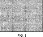
画像を作るピクセル値におけるある特定の種類のノイズ(暗電流ノイズと称される。図1を参照せよ)は、ランダムなノイズレベルを示す。ノイズレベルは、光がセンサによって受信されていてもいなくても、CMOSセンサアレイのそれぞれのピクセルによって生成される。(文言「ピクセル」は2つの異なる意味で用いられることがある。即ち、一つは、センサアレイの特定の位置にある光電性エレメントを言い、もう一つは、画像の特定の位置にありかつ輝度に対応する値を有するピクチャエレメントを言う。用語「デジタル画像」は、画像を作るピクセルアレイの値を述べるのに用いられることがある。)温度は別として、その暗電流レベルに影響を与える各センサピクセルの物理的特徴は、時間とともに変化しない。しかしながら、ピクセルの暗電流レベルは、ピクセルの温度による。さらに、ピクセルの暗電流は、時間とともに帯電を形成させる。それゆえピクセル値への暗電流の影響はピクセルの露光時間による。 One particular type of noise (referred to as dark current noise, see FIG. 1) in the pixel values that make up an image indicates a random noise level. The noise level is generated by each pixel of the CMOS sensor array, whether or not light is being received by the sensor. (The word “pixel” may be used in two different ways: one refers to a photoelectric element at a specific location in the sensor array, the other is at a specific location in the image and A picture element having a value corresponding to luminance.The term “digital image” may be used to describe the value of the pixel array that makes up the image.) Aside from temperature, it affects its dark current level. The physical characteristics of each sensor pixel do not change with time. However, the dark current level of the pixel depends on the temperature of the pixel. In addition, the dark current of the pixel causes a charge to form over time. Therefore, the effect of dark current on the pixel value depends on the exposure time of the pixel.
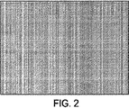
画像の他のアーチファクトは、縦縞パターン(固定パターンノイズとも称される)、オフセット、及びショットノイズを含む。縦縞パターン(図2を参照せよ)は、アレイの異なるカラムのそれぞれの読み出し回路の動作における意図せざる差によるものであり、通常、時間がたっても変化しない。オフセットは、画像から画像までの全信号レベル(輝度)における差を示し、差は、読み出し回路の特定の電気特性における変化によって生じる。センサアレイによって生成される各ピクセル値は、信号値に比例する変動を有するランダムなショットノイズを含む。 Other artifacts in the image include vertical stripe patterns (also called fixed pattern noise), offsets, and shot noise. The vertical stripe pattern (see FIG. 2) is due to an unintended difference in the operation of each readout circuit in different columns of the array and usually does not change over time. The offset indicates the difference in the total signal level (brightness) from image to image, and the difference is caused by a change in a particular electrical characteristic of the readout circuit. Each pixel value generated by the sensor array includes random shot noise having a variation proportional to the signal value.
他の種類の画像センサによって生成されるデジタル画像も暗電流ノイズの影響を受けやすいかもしれない。 Digital images generated by other types of image sensors may also be susceptible to dark current noise.
一般に、ターゲットデジタル画像は、画像センサから受信される。画像は、参照デジタル画像で表される大きさのわからないノイズが混入されている。ターゲットデジタル画像及び参照デジタル画像の統計的分析を用いてターゲットデジタル画像の少なくともいくつかのピクセルについてノイズの大きさを評価するプロセスが用いられる。 In general, a target digital image is received from an image sensor. The image is mixed with noise of unknown size represented by the reference digital image. A process is used that assesses the magnitude of noise for at least some pixels of the target digital image using statistical analysis of the target digital image and the reference digital image.
実施には以下の特徴のうちの1つまたは複数が含まれてもよい。センサは、CMOSセンサまたはCCDセンサである。ノイズは、暗電流ノイズを含む。プロセスは、ターゲットデジタル画像のあらゆるピクセルについて暗電流の大きさを評価する。プロセスは、プログラム命令を含む。統計的分析は、ターゲットデジタル画像と参照デジタル画像に関する無相関分析を含む。暗電流の大きさの評価は、センサ温度または露光時間についての情報を必要とせずに生成される。参照デジタル画像は暗電流デジタル画像に基づいており、暗電流デジタル画像は、実質的に縦縞パターンがなくて、それぞれ異なる露光時間を用いて得られるグレーデジタル画像と黒デジタル画像とから生成される。参照デジタル画像は、修正された暗電流デジタル画像に基づいており、修正された暗電流デジタル画像は、CMOSセンサのピクセルにわたって低頻度空間トレンドの影響を低減するように処理されている。参照デジタル画像は、トレンド除去された暗電流画像と黒デジタル画像との無相関性に基づいている。プロセスは、ターゲットデジタル画像からピクセルごとに縦縞パターンを引いて、縦縞パターンが修正されたデジタル画像を生成する。プロセスは、暗電流除去関数を縦縞パターンが修正されたデジタル画像に適用して、暗電流が修正されたデジタル画像を生成する。ターゲットデジタル画像のあらゆるピクセルのノイズは、評価された暗電流レベルを用いて低減される。プロセスは、オフセット評価及び減算関数を暗電流が修正されたデジタル画像に適用してオフセットを除去する。ノイズの低減されたターゲットデジタル画像は、CMOSセンサによって捕捉された画像の特徴の分析に用いるプロセッサに与えられる。ターゲットデジタル画像は、悪性病変を含んでいることがあるかもしれない。 Implementations may include one or more of the following features. The sensor is a CMOS sensor or a CCD sensor. The noise includes dark current noise. The process evaluates the magnitude of the dark current for every pixel of the target digital image. The process includes program instructions. Statistical analysis includes uncorrelated analysis on the target digital image and the reference digital image. An assessment of the magnitude of the dark current is generated without the need for information about sensor temperature or exposure time. The reference digital image is based on a dark current digital image, and the dark current digital image is generated from a gray digital image and a black digital image which are substantially free of vertical stripe patterns and are obtained using different exposure times. The reference digital image is based on a modified dark current digital image that has been processed to reduce the effects of low frequency spatial trends across the pixels of the CMOS sensor. The reference digital image is based on the decorrelation between the detrended dark current image and the black digital image. The process subtracts a vertical stripe pattern for each pixel from the target digital image to produce a digital image with the corrected vertical stripe pattern. The process applies a dark current removal function to the digital image with the corrected vertical stripe pattern to produce a digital image with corrected dark current. The noise of every pixel in the target digital image is reduced using the estimated dark current level. The process applies an offset estimation and subtraction function to the dark current modified digital image to remove the offset. The target digital image with reduced noise is provided to a processor that is used to analyze the characteristics of the image captured by the CMOS sensor. The target digital image may contain malignant lesions.
これらの特徴及び他の特徴並びに態様は、装置、方法、システム、プログラム製品、及び他の方法で表現されてもよい。 These and other features and aspects may be expressed in apparatus, methods, systems, program products, and other methods.
他の利点及び特徴は、以下の詳細な説明及び請求の範囲から明らかにされる。 Other advantages and features will be apparent from the following detailed description and from the claims.
図3に示すように、ターゲットシーン16(例えば、色素性病変18のある皮膚)から光学素子20を介して受信される光14に応じてCMOSセンサアレイ12によって生成される入力デジタル画像10(ターゲットとして、Tと称される)は、ノイズリダクションソフトウェア22(プロセッサ24によって実行される)によって(ストレージ38で一時的に記憶された後に)処理されて(例えば、ニューヨーク州アーヴィントンのエレクトロ‐オプティカルサイエンス社のメラノーマ検出製品であるメラファインド(MelaFind)(登録商標)を用いて、病斑が悪性メラノーマであるか否かを判断する(30)ために)、定量分析28で用いる出力デジタル画像26(Oと称される)を生成することができる。
As shown in FIG. 3, an input digital image 10 (target) generated by a
ノイズリダクションを医学的診断との関係におけるデジタル画像で実行する例が説明されているが、本ノイズリダクションプロセスは、いかなる目的に対するかついかなる状況下におけるいかなる画像センサアレイによって生成されるいかなるデジタル画像に対しても広く適用できる。例には、ノイズを低減したデジタル画像が、デジタル画像のノイズが問題になる最近の分析の対象となるいかなる例をも含んでいる。 While an example of performing noise reduction on a digital image in the context of a medical diagnosis is described, the noise reduction process can be applied to any digital image produced by any image sensor array for any purpose and under any circumstances. Even widely applicable. Examples include any example where a digital image with reduced noise is the subject of recent analysis where noise in the digital image is a problem.
縦縞パターン及びオフセットを低減する特定の方法も説明されているが、本明細書で説明されるデジタル画像の暗電流(及び参照デジタル画像で特徴付けられる他のノイズ)を低減する技術は、縦縞パターン及びオフセットがない限り、様々な用途で用いられてもよいし、または、当該技術において、他の種類のノイズが低減されてもよいし低減されなくてもよく、低減される場合には、リダクションは、本明細書で説明された例で説明される方法で行われてもよいし行われなくてもよい、ということが注目される。 Although specific methods for reducing vertical stripe patterns and offsets have also been described, techniques for reducing the dark current (and other noise characterized by reference digital images) described herein are described in vertical stripe patterns As long as there is no offset, it may be used in various applications, or in the art, other types of noise may or may not be reduced, and if reduced, reduction Note that may or may not be performed in the manner described in the examples described herein.
他の種類の処理がまた、様々な用途においてセンサで生成されるデジタル画像に関して必要とされるかもしれない。他の種類の処理には、特定のレンズ及び照明器に付随する光学的影響を修正する処理を含む。よって、本明細書で説明されるノイズリダクション技術には、あらゆる光学的修正または特定の種類の光学的修正によって限定されない用途がある。 Other types of processing may also be required for digital images generated with sensors in various applications. Other types of processing include processing to correct optical effects associated with specific lenses and illuminators. Thus, the noise reduction techniques described herein have applications that are not limited by any optical modification or specific type of optical modification.
図4A及び4Bに示すように、入力デジタル画像のノイズリダクション処理の前に、参照情報を取得して処理する。 As shown in FIGS. 4A and 4B, reference information is acquired and processed before noise reduction processing of the input digital image.
参照情報を展開処理するあるステップにおいて、グレーデジタル画像34の複数の独立したセットが、既知のセンサ温度または既知でないセンサ温度において暗部で取得されてストレージ38に記憶される。露光時間は、長時間露光からの飽和状態を回避してなお暗電流の信頼できる測定が行えるような中間範囲内にある。図5は、暗部で取得されるグレー画像の例(表示のために15倍の明度である)を示す。
In one step of developing the reference information, multiple independent sets of gray digital images 34 are acquired in the dark at a known sensor temperature or an unknown sensor temperature and stored in
複数のグレーデジタル画像は、平均化されて(39)、平均デジタル画像40(Gと称される)が生成され、平均デジタル画像40では、個々のピクセルのショットノイズのレベルが低減される。 The plurality of gray digital images are averaged (39) to produce an average digital image 40 (referred to as G), in which the level of shot noise of individual pixels is reduced.
また、入力デジタル画像のノイズリダクション処理の前に、縦縞パターンなどの固定パターンノイズがある場合、黒デジタル画像の複数の独立したセットが、暗部で取得される。黒のセットに対する露光時間は、グレーのセットに対するよりも短くて(例えば、ハードウェアが許容するできるだけ短い露光時間)、固定パターンノイズの信頼できる測定を行って黒のセットの暗電流レベルを最小にする。 Further, when there is fixed pattern noise such as a vertical stripe pattern before noise reduction processing of the input digital image, a plurality of independent sets of black digital images are acquired in the dark part. The exposure time for the black set is shorter than for the gray set (for example, the shortest exposure time that the hardware allows) and a reliable measurement of fixed pattern noise is made to minimize the dark current level of the black set. To do.
複数の黒画像は、平均化されて(39)、平均黒デジタル画像44(Bと称される)を生成し、平均黒デジタル画像44では、平均グレーデジタル画像についてのように、個々のピクセルのショットノイズの影響が低減される。
The multiple black images are averaged (39) to produce an average black digital image 44 (referred to as B), where the average black
平均黒デジタル画像Bが平均グレーデジタル画像Gから引かれて(46)、暗電流デジタル画像48(D)が生成される。グレーデジタル画像からの黒デジタル画像を引くことによって、純粋な暗電流の画像(縦縞パターンがない)が生成される。図6は、縦縞パターンを引いた後の図5の画像(表示のために15倍の明度である)を示す。 The average black digital image B is subtracted from the average gray digital image G (46) to produce a dark current digital image 48 (D). By subtracting a black digital image from a gray digital image, a pure dark current image (no vertical stripe pattern) is generated. FIG. 6 shows the image of FIG. 5 (with 15 times the brightness for display) after drawing the vertical stripe pattern.
次に、トレンド除去関数が暗電流デジタル画像48に適用されて(50)、データ48のピクセルから低頻度空間トレンドが除去される。なんとなれば、暗電流デジタル画像のトレンドは、ターゲットデジタル画像と相関性があるからである。このトレンド除去は、暗電流デジタル画像48のアレイ全体をNピクセル×Nピクセルのサブアレイに再分割することによって行われる。各サブアレイ内で、暗電流デジタル画像値が、最小二乗適合を用いて、2つの変数の二次関数に適用される。次に、各ピクセルに対するこの二次関数の値は、当該ピクセルの実際の暗電流値から引かれる。実際には、N=3で良好な結果が得られた。結果は、トレンド除去した暗電流デジタル画像52(S)である。 A detrending function is then applied to the dark current digital image 48 (50) to remove the low frequency spatial trend from the pixels of the data 48. This is because the trend of the dark current digital image is correlated with the target digital image. This detrending is done by subdividing the entire array of dark current digital images 48 into sub-arrays of N pixels × N pixels. Within each subarray, dark current digital image values are applied to a quadratic function of two variables using a least squares fit. The value of this quadratic function for each pixel is then subtracted from the actual dark current value for that pixel. In practice, good results were obtained with N = 3. The result is a dark current digital image 52 (S) from which the trend has been removed.
次に、純粋な縦縞パターンデジタル画像V56が、暗電流除去関数(54)をBに最初に適用することによって生成される。一般に、除去関数は、デジタル画像を返す。デジタル画像は、(i)入力デジタル画像と、(ii)暗電流デジタル画像Dを要因A1倍した積と、の間のピクセルごとの差を示す。
V=B−A1*D
ここで、無相関関数は、2セットのデジタル画像、即ちB及びSに関して要因A1を見出す。
相関(B−A1*S,S)=0
ここで、相関は、画像の特定領域内のすべてのピクセルにわたって算出される。
A pure vertical stripe pattern digital image V56 is then generated by first applying a dark current removal function (54) to B. In general, the removal function returns a digital image. The digital image shows the pixel-by-pixel difference between (i) the input digital image and (ii) the product of the dark current digital image D multiplied by factor A1.
V = B-A1 * D
Here, the decorrelation function finds the factor A1 for two sets of digital images, namely B and S.
Correlation (B-A1 * S, S) = 0
Here, the correlation is calculated over all the pixels in a specific region of the image.
言い換えると、無相関関数は、画像のいくつかの領域にわたってデジタル画像Sからデジタル画像Bを無相関にする要因A1を判別する。図4の特定のステップ54に関して、無相関によって、黒画像Bにおける暗電流Dの大きさ(A1)が判別される。
In other words, the decorrelation function determines a factor A1 that makes the digital image B uncorrelated from the digital image S over several regions of the image. With respect to the
無相関関数は、センサ温度または露光時間を知る必要なしにターゲットピクセルからかつ参照ピクセルから暗電流ノイズが判別され得るようにする統計的分析の例である。分散最小化分析などの他の統計的方法が用いられてもよい。図のステップ54の結果は、純粋な縦縞パターンのデジタル画像V56である。
The decorrelation function is an example of a statistical analysis that allows dark current noise to be determined from the target pixel and from the reference pixel without having to know the sensor temperature or exposure time. Other statistical methods such as variance minimization analysis may be used. The result of
図7は、暗電流ノイズを引いた後の図6の画像を示す(15レベル及び100レベルで乗算された明度が表示のために各ピクセルに加えられた)。 FIG. 7 shows the image of FIG. 6 after dark current noise is subtracted (brightness multiplied by 15 and 100 levels added to each pixel for display).
図8は、明度を調節していない図5、6及び7の画像の標本図を示す。図8では、VRemは、固定パターンノイズを引いた後の明度である。DCRemは、固定パターンノイズ及び暗電流を引いた後の明度である。OffRemは、固定パターンノイズ、暗電流、及びオフセットを引いた後の明度である。図5のオリジナル画像では、ショットノイズは、約7−8レベルであり、ショットノイズは、較正プロセスによって除去されない。ショットノイズのリダクションは、画像についての空間の平均化または一時的な平均化のいずれかを必要とするかもしれない。 FIG. 8 shows a sample diagram of the images of FIGS. 5, 6 and 7 without adjusting the brightness. In FIG. 8, VRem is the brightness after subtracting the fixed pattern noise. DCRem is the brightness after subtracting fixed pattern noise and dark current. OffRem is the lightness after subtracting fixed pattern noise, dark current, and offset. In the original image of FIG. 5, shot noise is about 7-8 levels and shot noise is not removed by the calibration process. Shot noise reduction may require either spatial or temporal averaging of the image.
上述のステップは、例えば、係数較正の間一度だけ実行される必要があり、得られる較正デジタル画像は、長期にわたって多数のターゲット画像のために記憶されて用いられてもよい。ターゲット画像が捕捉されるたびに再び較正画像情報を展開処理する必要はない。 The above steps need only be performed once during coefficient calibration, for example, and the resulting calibration digital image may be stored and used for multiple target images over time. There is no need to develop the calibration image information again each time a target image is captured.
図4Bに示したように、Tのノイズを低減するために、純粋な縦縞パターンのデジタル画像Vが、Tから、ピクセルごとに引かれて、縦縞パターンが修正されたデジタル画像T1が得られる(60)。
T1=T−V
次に、画像のいくつかの領域にわたって無相関関数(54)を用いて、画像T1の当該領域の暗電流Dの大きさA2が、
相関(T1−A2*S,S)=0
から判別され、次に、暗電流がT1から除去されて、暗電流の修正されたデジタル画像T2が生成される(64)。
T2=T1−A2*D
CMOSセンサは、(ターゲットからのあらゆる光を含む)光から映されるアレイの(例えば、コーナーのまたはエッジの1つに沿った)黒領域を有するように配置され得る。黒領域からのデジタル画像は、画像内のオフセットを修正するために用いられ得る。黒領域デジタル画像は、前に説明した縦縞パターン除去ステップ及び暗電流除去ステップによって最初に処理され、得られた処理済みの黒領域データが、平均化されて(66)、平均黒領域値NBが生成される(68)。平均黒領域値が、画像の暗電流が修正されたデジタル画像T2のあらゆるピクセルから引かれて(70)、ターゲット画像からオフセットが排除される。得られたオフセットが修正されたデジタル画像T3(72)は、状況により追加の処理を受けてもよい。
As shown in FIG. 4B, in order to reduce the noise of T, a digital image V with a pure vertical stripe pattern is subtracted from T for each pixel to obtain a digital image T1 with a corrected vertical stripe pattern ( 60).
T1 = TV
Next, using the decorrelation function (54) over several regions of the image, the magnitude A2 of the dark current D in that region of the image T1 is
Correlation (T1-A2 * S, S) = 0
It is determined from, then dark current is removed from T1, the digital image T2 which has been modified dark current is generated (64).
T2 = T1-A2 * D
The CMOS sensor can be arranged to have a black area (eg, along one of the corners or edges) of the array that is imaged from light (including any light from the target). A digital image from the black region can be used to correct the offset in the image. The black area digital image is first processed by the vertical stripe pattern removal step and dark current removal step described above, and the obtained processed black area data is averaged (66) to obtain an average black area value NB. Is generated (68). The average black area value is subtracted (70) from every pixel of the digital image T2 in which the dark current of the image has been modified to eliminate the offset from the target image. The obtained digital image T3 (72) in which the offset is corrected may be subjected to additional processing depending on the situation.
例えば、画像システムによって与えられる不均一性(一様でないターゲット照明または不均一なセンサ応答など)によるデジタル画像T3からのアーチファクトを除去することに関心があるかまたはデジタル画像T3の実際の反射率を判別することに関心がある場合、較正デジタル画像Wは、既知の拡散反射率を有する均一のホワイトターゲットを撮像することによって取得されてもよい。次に、このホワイトターゲットデジタル画像は、縦縞パターン除去(該当する場合、Vを引くこと)、無相関性をW‐V及びSに適用することによって暗電流の大きさを判別すること、暗電流除去、並びに、オフセット除去、を含む一連の工程を受けてW1を生成する。反射率較正78は、デジタル画像T3に適用されて、(ピクセルごとに実行される)以下の計算によって反射率デジタル画像T4が生成されてもよい(80)。
T4=(T3/W)*(E(W)/E(T3))*ρ
ここで、Eは露光時間であり、ρはホワイト較正ターゲットの反射率である。反射率較正78は、画像システムによって与えられる不均一性をデジタル画像T3から除去する。
For example, you are interested in removing artifacts from the digital image T3 due to non-uniformities provided by the imaging system (such as non-uniform target illumination or non-uniform sensor response) or the actual reflectivity of the digital image T3. If interested in discriminating , the calibration digital image W may be acquired by imaging a uniform white target having a known diffuse reflectance. Next, this white target digital image is obtained by determining the magnitude of dark current by removing vertical stripe pattern (subtracting V, if applicable), applying uncorrelation to WV and S, dark current W1 is generated through a series of steps including removal and offset removal. The
T4 = (T3 / W) * (E (W) / E (T3)) * ρ
Where E is the exposure time and ρ is the reflectance of the white calibration target. The
必要に応じ追加の処理がT4に行われて、出力画像Oを生成する。 If necessary, additional processing is performed at T4 to generate the output image O.
上述のプロセスは、センサアレイのすべての位置においてセンサ温度が均一であると仮定する。温度はセンサ全域で変化するという事実に対応させるために、暗電流は、センサの異なる部分で独立して評価されてもよく、独立した評価は入力デジタル画像の対応する部分に別個に適用された。 The above process assumes that the sensor temperature is uniform at all locations in the sensor array. To accommodate the fact that the temperature varies across the sensor, dark current may be evaluated independently at different parts of the sensor, and the independent evaluation was applied separately to the corresponding part of the input digital image. .
上述のプロセスは、センサによって提供される単色のデジタル画像に適用され得る。いくつかの例では、プロセスは、センサによって同時に生成される異なるスペクトル領域の複数のデジタル画像に適用されてもよい(例えば、赤、緑、及び青‐RGB)。かかる場合、異なるスペクトル領域のデジタル画像は、上記のように独立して処理されてもよい。 The process described above can be applied to monochromatic digital images provided by sensors. In some examples, the process may be applied to multiple digital images in different spectral regions that are generated simultaneously by the sensor (eg, red, green, and blue-RGB). In such a case, digital images in different spectral regions may be processed independently as described above.
プロセスは、いくつかのセンサに対して、暗電流ノイズの影響を低減する方法として温度または露光時間を制御する必要性を減らす統計的分析を利用してもよい。 The process may utilize statistical analysis to reduce the need to control temperature or exposure time as a way to reduce the effects of dark current noise for some sensors.
上述のプロセスは、ハードウェア、ソフトウェア、もしくはファームウェア、またはそれらの任意の組み合わせで実行されてもよい。 The above process may be performed in hardware, software, or firmware, or any combination thereof.
暗電流評価技術の検証は、上述の評価技術によって予測される暗電流レベルに対して温度と湿度等が調整された環境において様々な露光時間で特に得られる暗画像から取り出された暗電流レベルを比較することによって実行された。無相関ベースの推定器は、図9に示したように、避けられないショットノイズが出現した場合においてでさえ個々の画像の実際の暗電流レベルを正確に予測することができるということが証明された。 The verification of the dark current evaluation technique is based on the dark current level extracted from a dark image obtained at various exposure times in an environment where the temperature and humidity are adjusted with respect to the dark current level predicted by the above-described evaluation technique. Performed by comparing. An uncorrelated based estimator has proven to be able to accurately predict the actual dark current level of individual images even in the event of inevitable shot noise, as shown in FIG. It was.
他の実施例は、請求の範囲内にある。例えば、分散最小化分析が、無相関分析に代替されてもよい。 Other embodiments are within the scope of the claims. For example, variance minimization analysis may be substituted for decorrelation analysis.
本明細書で説明した技術は、可視領域及び赤外領域内のセンサ動作に対してだけでなく、x線及び場合によっては超音波に対して、即ち、暗電流ノイズの除去または暗電流ノイズと同様の影響の除去に有用であるかもしれないいかなるセンサに対しても有用であるだろう。 The techniques described herein are not only for sensor operation in the visible and infrared regions, but also for x-rays and possibly ultrasound, ie, dark current noise removal or dark current noise. It would be useful for any sensor that might be useful for removing similar effects.
上記の検討は、暗電流ノイズ修正を対象としているが、同様の技術は、参照画像の任意のノイズが既知であるかまたは取得され得る他の状況でかつターゲットデジタル画像のノイズの大きさが分からないといった他の状況で用いられてもよい。 Although the above discussion is directed to dark current noise correction, similar techniques can be used to determine the magnitude of noise in the target digital image in other situations where any noise in the reference image is known or can be acquired. It may be used in other situations, such as none.
Claims (24)
前記大きさは異なるデジタル画像で異なる可能性があり、前記判別は、前記デジタル画像Tと、前記汚染しているノイズの代表画像である参照デジタル画像と、に基づいてなされ、 The size may be different for different digital images, and the determination is made based on the digital image T and a reference digital image that is a representative image of the contaminating noise,
前記デジタル画像Tと前記参照デジタル画像は同一のセンサによって取得され、 The digital image T and the reference digital image are acquired by the same sensor,
前記判別は無相関関係すなわち(T−A*{前記参照デジタル画像},{前記参照デジタル画像})=0の相関の下でなされ、 The discrimination is made under non-correlation, that is, (T-A * {the reference digital image}, {the reference digital image}) = 0 correlation,
前記判別はT及び前記参照デジタル画像の幾つかの領域におけるピクセルにわたってなされて、Tの少なくとも幾つかのピクセルの各々について前記ノイズの大きさを評価することを特徴とする方法。 The method is characterized in that the determination is made across pixels in T and several regions of the reference digital image to evaluate the noise magnitude for each of at least some pixels of T.
前記ソフトウェアプロセッサは、 The software processor is
任意のターゲットであるデジタル画像Tのピクセルの少なくとも幾つかを汚染しているノイズのわからない大きさAを判別し、 Determine the unknown magnitude A of noise that is contaminating at least some of the pixels of the digital image T, which is an arbitrary target,
前記大きさは異なるデジタル画像で異なる可能性があり、前記判別は、前記デジタル画像Tと、前記汚染しているノイズの代表画像である参照デジタル画像と、に基づいてなされ、 The size may be different for different digital images, and the determination is made based on the digital image T and a reference digital image that is a representative image of the contaminating noise,
前記デジタル画像Tと前記参照デジタル画像は同一のセンサによって取得され、 The digital image T and the reference digital image are acquired by the same sensor,
前記判別は無相関関係すなわち(T−A*{前記参照デジタル画像},{前記参照デジタル画像})=0の相関の下でなされ、 The discrimination is made under non-correlation, that is, (T-A * {the reference digital image}, {the reference digital image}) = 0 correlation,
前記判別はT及び前記参照デジタル画像の幾つかの領域におけるピクセルにわたってなされて、Tの少なくとも幾つかのピクセルの各々について前記ノイズの大きさを評価する、 The discrimination is made across pixels in T and some regions of the reference digital image to evaluate the noise magnitude for each of at least some pixels in T.
ように構成されていることを特徴とする装置。 An apparatus characterized by being configured as follows.
前記デジタル画像Tのピクセルの少なくとも幾つかを汚染しているノイズのわからない大きさAを判別する判別する手段と、を含み、 Means for determining an unknown magnitude A of noise contaminating at least some of the pixels of the digital image T;
前記大きさは異なるデジタル画像で異なる可能性があり、前記判別は、前記デジタル画像Tと、前記汚染しているノイズの代表画像である参照デジタル画像と、に基づいてなされ、 The size may be different for different digital images, and the determination is made based on the digital image T and a reference digital image that is a representative image of the contaminating noise,
前記デジタル画像Tと前記参照デジタル画像は同一のセンサによって取得され、 The digital image T and the reference digital image are acquired by the same sensor,
前記判別は無相関関係すなわち(T−A*{前記参照デジタル画像},{前記参照デジタル画像})=0の相関の下でなされ、 The discrimination is made under non-correlation, that is, (T-A * {the reference digital image}, {the reference digital image}) = 0 correlation,
前記判別はT及び前記参照デジタル画像の幾つかの領域におけるピクセルにわたってなされて、Tの少なくとも幾つかのピクセルの各々について前記ノイズの大きさを評価する装置。 An apparatus for determining the magnitude of the noise for each of at least some pixels of T, wherein the discrimination is made across pixels in T and some regions of the reference digital image.
Applications Claiming Priority (3)
| Application Number | Priority Date | Filing Date | Title |
|---|---|---|---|
| US11/500,197 US7813586B2 (en) | 2006-08-07 | 2006-08-07 | Reducing noise in digital images |
| US11/500,197 | 2006-08-07 | ||
| PCT/US2007/075333 WO2008019358A2 (en) | 2006-08-07 | 2007-08-07 | Reducing noise in digital images |
Publications (3)
| Publication Number | Publication Date |
|---|---|
| JP2010500125A JP2010500125A (en) | 2010-01-07 |
| JP2010500125A5 JP2010500125A5 (en) | 2011-10-13 |
| JP5198449B2 true JP5198449B2 (en) | 2013-05-15 |
Family
ID=39029242
Family Applications (1)
| Application Number | Title | Priority Date | Filing Date |
|---|---|---|---|
| JP2009523947A Expired - Fee Related JP5198449B2 (en) | 2006-08-07 | 2007-08-07 | How to reduce noise in digital images |
Country Status (6)
| Country | Link |
|---|---|
| US (3) | US7813586B2 (en) |
| EP (1) | EP2054843A4 (en) |
| JP (1) | JP5198449B2 (en) |
| AU (1) | AU2007281748B2 (en) |
| CA (1) | CA2660337C (en) |
| WO (1) | WO2008019358A2 (en) |
Families Citing this family (40)
| Publication number | Priority date | Publication date | Assignee | Title |
|---|---|---|---|---|
| US7813586B2 (en) | 2006-08-07 | 2010-10-12 | Mela Sciences, Inc. | Reducing noise in digital images |
| US10298834B2 (en) | 2006-12-01 | 2019-05-21 | Google Llc | Video refocusing |
| JP5075648B2 (en) * | 2008-01-15 | 2012-11-21 | オリンパス株式会社 | Image processing apparatus, image processing program, and image processing method |
| US8094215B2 (en) * | 2008-10-02 | 2012-01-10 | Altasens, Inc. | Digital column gain mismatch correction for 4T CMOS imaging systems-on-chip |
| US8381987B2 (en) * | 2009-07-30 | 2013-02-26 | Mela Sciences, Inc. | Insertable storage card containing a portable memory card having a connection interface |
| US8286977B2 (en) * | 2009-07-30 | 2012-10-16 | Mela Sciences, Inc. | Medical cart |
| KR20110048922A (en) * | 2009-11-03 | 2011-05-12 | 삼성전자주식회사 | Method of modeling integrated noise and method of reducing noises in image sensors |
| JP5523065B2 (en) * | 2009-11-13 | 2014-06-18 | キヤノン株式会社 | Imaging apparatus and control method thereof |
| US9858649B2 (en) | 2015-09-30 | 2018-01-02 | Lytro, Inc. | Depth-based image blurring |
| US9559039B2 (en) * | 2012-09-17 | 2017-01-31 | STATS ChipPAC Pte. Ltd. | Semiconductor device and method of using substrate having base and conductive posts to form vertical interconnect structure in embedded die package |
| EP2967296B1 (en) * | 2013-03-15 | 2024-02-28 | DePuy Synthes Products, Inc. | Comprehensive fixed pattern noise cancellation |
| US10334151B2 (en) | 2013-04-22 | 2019-06-25 | Google Llc | Phase detection autofocus using subaperture images |
| JP6397191B2 (en) * | 2014-01-24 | 2018-09-26 | オリンパス株式会社 | Optical scanning observation device |
| US9560294B2 (en) * | 2014-12-10 | 2017-01-31 | Semiconductor Components Industries, Llc | Systems and methods for pixel-level dark current compensation in image sensors |
| US10412373B2 (en) | 2015-04-15 | 2019-09-10 | Google Llc | Image capture for virtual reality displays |
| US10567464B2 (en) | 2015-04-15 | 2020-02-18 | Google Llc | Video compression with adaptive view-dependent lighting removal |
| US10565734B2 (en) | 2015-04-15 | 2020-02-18 | Google Llc | Video capture, processing, calibration, computational fiber artifact removal, and light-field pipeline |
| US10341632B2 (en) | 2015-04-15 | 2019-07-02 | Google Llc. | Spatial random access enabled video system with a three-dimensional viewing volume |
| US10546424B2 (en) | 2015-04-15 | 2020-01-28 | Google Llc | Layered content delivery for virtual and augmented reality experiences |
| US10540818B2 (en) | 2015-04-15 | 2020-01-21 | Google Llc | Stereo image generation and interactive playback |
| US10419737B2 (en) | 2015-04-15 | 2019-09-17 | Google Llc | Data structures and delivery methods for expediting virtual reality playback |
| US10469873B2 (en) | 2015-04-15 | 2019-11-05 | Google Llc | Encoding and decoding virtual reality video |
| US11328446B2 (en) | 2015-04-15 | 2022-05-10 | Google Llc | Combining light-field data with active depth data for depth map generation |
| US10275898B1 (en) | 2015-04-15 | 2019-04-30 | Google Llc | Wedge-based light-field video capture |
| US10444931B2 (en) | 2017-05-09 | 2019-10-15 | Google Llc | Vantage generation and interactive playback |
| US10440407B2 (en) | 2017-05-09 | 2019-10-08 | Google Llc | Adaptive control for immersive experience delivery |
| US9979909B2 (en) | 2015-07-24 | 2018-05-22 | Lytro, Inc. | Automatic lens flare detection and correction for light-field images |
| US9984438B1 (en) | 2016-02-09 | 2018-05-29 | Goodrich Corporation | Robust image registration for multi-spectral/multi-modality imagery |
| US20170256036A1 (en) * | 2016-03-03 | 2017-09-07 | Lytro, Inc. | Automatic microlens array artifact correction for light-field images |
| US10223331B2 (en) | 2016-04-08 | 2019-03-05 | Goodrich Corporation | Warp models for registering multi-spectral imagery |
| US10275892B2 (en) | 2016-06-09 | 2019-04-30 | Google Llc | Multi-view scene segmentation and propagation |
| US10679361B2 (en) | 2016-12-05 | 2020-06-09 | Google Llc | Multi-view rotoscope contour propagation |
| US10594945B2 (en) | 2017-04-03 | 2020-03-17 | Google Llc | Generating dolly zoom effect using light field image data |
| US10474227B2 (en) | 2017-05-09 | 2019-11-12 | Google Llc | Generation of virtual reality with 6 degrees of freedom from limited viewer data |
| US10354399B2 (en) | 2017-05-25 | 2019-07-16 | Google Llc | Multi-view back-projection to a light-field |
| US10545215B2 (en) | 2017-09-13 | 2020-01-28 | Google Llc | 4D camera tracking and optical stabilization |
| US10965862B2 (en) | 2018-01-18 | 2021-03-30 | Google Llc | Multi-camera navigation interface |
| US11854162B2 (en) | 2019-02-18 | 2023-12-26 | Georgia Tech Research Corporation | Microscopy with near-ideal sCMOS camera |
| US11756285B2 (en) | 2021-06-10 | 2023-09-12 | Bank Of America Corporation | Image processing system and method for image noise removal |
| DE102021209634A1 (en) | 2021-09-01 | 2023-03-02 | Volkswagen Aktiengesellschaft | Roof system for a motor vehicle, motor vehicle |
Family Cites Families (73)
| Publication number | Priority date | Publication date | Assignee | Title |
|---|---|---|---|---|
| GB1523232A (en) | 1976-03-31 | 1978-08-31 | Elliott Brothers London Ltd | Electronic arragements including charge coupled devices |
| DE2714777C2 (en) | 1977-04-02 | 1982-02-11 | Messerschmitt-Bölkow-Blohm GmbH, 8000 München | Circuit arrangement for correcting each individual pixel signal of a signal sequence of a photoelectric image converter system that has been converted into digital form |
| US4341956A (en) | 1979-09-24 | 1982-07-27 | Pfizer, Inc. | Apparatus and method for compensating the dark current photoelectric transducers |
| US4606004A (en) * | 1984-03-21 | 1986-08-12 | General Electric Company | Apparatus for reduction of filtration truncation errors |
| JPS61100080A (en) | 1984-10-22 | 1986-05-19 | Canon Inc | Solid-state image pickup device |
| US4599654A (en) | 1984-10-31 | 1986-07-08 | Rca Corporation | Dark current eliminator useful for auto-iris controller |
| US4739495A (en) | 1985-09-25 | 1988-04-19 | Rca Corporation | Solid-state imager defect corrector |
| US4703442A (en) | 1985-09-25 | 1987-10-27 | Rca Corporation | Temperature tracking defect corrector for a solid-state imager |
| US4916307A (en) | 1987-12-15 | 1990-04-10 | Fuji Electric Co., Ltd. | Light intensity detecting circuit with dark current compensation |
| US4972267A (en) | 1988-06-14 | 1990-11-20 | Fuji Photo Film Co., Ltd. | Still-video camera for eliminating dark current differences |
| US4984085A (en) | 1989-08-03 | 1991-01-08 | Allen-Bradley Company, Inc. | Image processor with dark current compensation |
| US5115458A (en) | 1989-09-05 | 1992-05-19 | Eastman Kodak Company | Reducing dark current in charge coupled devices |
| US5153732A (en) | 1990-02-16 | 1992-10-06 | Fuji Photo Film Co., Ltd. | Electronic still camera which reduces the influence of smear and dark current |
| US5272536A (en) | 1990-03-13 | 1993-12-21 | Sony Corporation | Dark current and defective pixel correction apparatus |
| JP2802962B2 (en) | 1990-05-25 | 1998-09-24 | 旭光学工業株式会社 | Image sensor drive |
| US5355164A (en) | 1990-06-25 | 1994-10-11 | Fuji Photo Film Co., Ltd. | Method and apparatus of correction image read signals by removing the influence of dark current therefrom |
| JP3311004B2 (en) | 1991-03-28 | 2002-08-05 | 株式会社東芝 | Solid-state imaging device |
| SE9201482L (en) | 1992-05-11 | 1993-11-12 | Regam Medical Systems Ab | Method for compensating dark current at CCd sensor for dental x-ray |
| JP3285928B2 (en) | 1992-05-27 | 2002-05-27 | 株式会社東芝 | Solid-state imaging device |
| CA2110865C (en) | 1992-12-08 | 1998-07-14 | Naoshi Suzuki | Dark current compensation of pixels tracking stars several times |
| US5408314A (en) | 1993-02-24 | 1995-04-18 | Perry; Jeffrey | Dark current subtraction with abbreviated reference cycles and recursive filtering |
| JP2747410B2 (en) | 1993-05-21 | 1998-05-06 | 富士通株式会社 | Solid-state imaging device |
| JP3310404B2 (en) | 1993-07-23 | 2002-08-05 | 浜松ホトニクス株式会社 | Cooling type solid-state imaging device |
| FR2722635B1 (en) | 1994-07-12 | 1996-08-23 | Thomson Csf Semiconducteurs | PHOTODETECTOR DARK CURRENT SUPPRESSION CIRCUIT |
| US5565674A (en) | 1994-09-13 | 1996-10-15 | Eastman Kodak Company | Optical detection and signal conditioning package |
| DE69625398T2 (en) * | 1995-02-24 | 2003-09-04 | Eastman Kodak Co | Black pattern correction for a charge transfer sensor |
| JPH0961236A (en) * | 1995-08-21 | 1997-03-07 | Fujitsu Ltd | Signal processor for photoelectric transducing element |
| US6271880B1 (en) | 1996-02-26 | 2001-08-07 | Canon Kabushiki Kaisha | Apparatus having a photoelectric conversion element and a transistor, in which the duration of the on time of the transistor is based on a detected temperature of the conversion element or transistor |
| JP3384673B2 (en) | 1996-03-12 | 2003-03-10 | 三洋電機株式会社 | Digital video camera |
| JPH09298647A (en) | 1996-05-01 | 1997-11-18 | Fuji Photo Film Co Ltd | Offset level correction method for linear image sensor and device therefor |
| GB2317522B (en) * | 1996-09-12 | 2000-09-27 | Vsli Vision Limited | Low noise operation of an image sensor |
| US6081612A (en) * | 1997-02-28 | 2000-06-27 | Electro Optical Sciences Inc. | Systems and methods for the multispectral imaging and characterization of skin tissue |
| US6208749B1 (en) * | 1997-02-28 | 2001-03-27 | Electro-Optical Sciences, Inc. | Systems and methods for the multispectral imaging and characterization of skin tissue |
| DE19734717A1 (en) | 1997-08-11 | 1999-02-25 | Sirona Dental Systems Gmbh | Method for compensating the dark current when creating dental panoramic and / or cephalometric slice images |
| DE19818975A1 (en) * | 1997-08-12 | 1999-02-18 | Hewlett Packard Co | Method for correcting dark current in CMOS imaging sensors |
| US6362482B1 (en) | 1997-09-16 | 2002-03-26 | Advanced Scientific Concepts, Inc. | High data rate smart sensor technology |
| US6369853B1 (en) | 1997-11-13 | 2002-04-09 | Foveon, Inc. | Intra-pixel frame storage element, array, and electronic shutter method suitable for electronic still camera applications |
| US6452633B1 (en) | 1998-02-26 | 2002-09-17 | Foveon, Inc. | Exposure control in electronic cameras by detecting overflow from active pixels |
| FR2782809B1 (en) | 1998-05-15 | 2005-08-26 | Asahi Optical Co Ltd | DETECTION DEVICE FOR DEVELOPING STATUS |
| US6101287A (en) | 1998-05-27 | 2000-08-08 | Intel Corporation | Dark frame subtraction |
| US6525769B1 (en) | 1998-12-30 | 2003-02-25 | Intel Corporation | Method and apparatus to compensate for dark current in an imaging device |
| US6614562B1 (en) | 1999-06-30 | 2003-09-02 | Intel Corporation | Reducing dark current noise in an imaging system |
| IL131242A0 (en) | 1999-08-04 | 2001-01-28 | Given Imaging Ltd | A method for temperature sensing |
| US6798456B1 (en) | 1999-09-03 | 2004-09-28 | Pentax Corporation | Exposure period control device for electronic still camera |
| US6707557B2 (en) | 1999-12-30 | 2004-03-16 | Eastman Kodak Company | Method and system for estimating sensor dark current drift and sensor/illumination non-uniformities |
| GB2361994B (en) * | 2000-05-06 | 2004-12-08 | Astron Clinica Ltd | Apparatus and methods for analysing skin histology |
| JP2001339643A (en) | 2000-05-30 | 2001-12-07 | Nec Corp | Black level generating circuit for solid-state image pickup device and solid-state image pickup device |
| US6271054B1 (en) | 2000-06-02 | 2001-08-07 | International Business Machines Corporation | Method for reducing dark current effects in a charge couple device |
| JP3897520B2 (en) * | 2000-07-11 | 2007-03-28 | キヤノン株式会社 | IMAGING DEVICE AND IMAGING DEVICE CONTROL METHOD |
| US6352482B1 (en) * | 2000-08-31 | 2002-03-05 | Callaway Golf Company | Golf club with hosel liner |
| US6995795B1 (en) | 2000-09-12 | 2006-02-07 | Eastman Kodak Company | Method for reducing dark current |
| US6917380B1 (en) | 2000-10-05 | 2005-07-12 | Ess Technology, Inc. | One time programmable solid-state device |
| JP2002222416A (en) * | 2001-01-26 | 2002-08-09 | Mitsubishi Electric Corp | Picture quality improving device |
| US6700654B2 (en) | 2001-02-15 | 2004-03-02 | Corning Incorporated | Automatic dark current compensation |
| US6714241B2 (en) | 2001-04-25 | 2004-03-30 | Hewlett-Packard Development Company, L.P. | Efficient dark current subtraction in an image sensor |
| US6756651B2 (en) | 2001-09-26 | 2004-06-29 | International Business Machines Corporation | CMOS-compatible metal-semiconductor-metal photodetector |
| US7064785B2 (en) | 2002-02-07 | 2006-06-20 | Eastman Kodak Company | Apparatus and method of correcting for dark current in a solid state image sensor |
| US7102672B1 (en) | 2002-02-08 | 2006-09-05 | Electro Optical Sciences Inc | Integrated CMOS imaging array dark current monitor |
| US7015448B2 (en) | 2002-08-22 | 2006-03-21 | Micron Technology, Inc. | Dark current reduction circuitry for CMOS active pixel sensors |
| JP2004236167A (en) * | 2003-01-31 | 2004-08-19 | Fuji Photo Film Co Ltd | Image reader |
| EP1447977A1 (en) * | 2003-02-12 | 2004-08-18 | Dialog Semiconductor GmbH | Vignetting compensation |
| US7015960B2 (en) | 2003-03-18 | 2006-03-21 | Candela Microsystems, Inc. | Image sensor that uses a temperature sensor to compensate for dark current |
| US6977364B2 (en) | 2003-07-28 | 2005-12-20 | Asml Holding N.V. | System and method for compensating for dark current in photosensitive devices |
| US7064406B2 (en) | 2003-09-03 | 2006-06-20 | Micron Technology, Inc. | Supression of dark current in a photosensor for imaging |
| US7394929B2 (en) * | 2003-09-24 | 2008-07-01 | Hewlett-Packard Development Company, L.P. | Digital picture image color conversion |
| JP2005110176A (en) * | 2003-10-02 | 2005-04-21 | Nikon Corp | Noise removing method, noise removing processing program, and noise removing device |
| JP2005204810A (en) * | 2004-01-21 | 2005-08-04 | Canon Inc | X-ray imaging apparatus |
| US7053354B1 (en) | 2004-05-24 | 2006-05-30 | Eastman Kodak Company | Method for reducing dark current for an array of active pixel sensor cells |
| US7961973B2 (en) * | 2004-09-02 | 2011-06-14 | Qualcomm Incorporated | Lens roll-off correction method and apparatus |
| US20060262210A1 (en) * | 2005-05-19 | 2006-11-23 | Micron Technology, Inc. | Method and apparatus for column-wise suppression of noise in an imager |
| US7969488B2 (en) * | 2005-08-03 | 2011-06-28 | Micron Technologies, Inc. | Correction of cluster defects in imagers |
| US7813586B2 (en) * | 2006-08-07 | 2010-10-12 | Mela Sciences, Inc. | Reducing noise in digital images |
| KR101544032B1 (en) * | 2008-12-16 | 2015-08-12 | 삼성전자주식회사 | Method and apparatus for removing image noise |
-
2006
- 2006-08-07 US US11/500,197 patent/US7813586B2/en active Active
-
2007
- 2007-08-07 EP EP07840735A patent/EP2054843A4/en not_active Withdrawn
- 2007-08-07 JP JP2009523947A patent/JP5198449B2/en not_active Expired - Fee Related
- 2007-08-07 WO PCT/US2007/075333 patent/WO2008019358A2/en active Application Filing
- 2007-08-07 CA CA2660337A patent/CA2660337C/en not_active Expired - Fee Related
- 2007-08-07 AU AU2007281748A patent/AU2007281748B2/en not_active Ceased
-
2010
- 2010-10-06 US US12/898,802 patent/US8160386B2/en active Active - Reinstated
-
2012
- 2012-03-01 US US13/409,397 patent/US8630508B2/en not_active Expired - Fee Related
Also Published As
| Publication number | Publication date |
|---|---|
| WO2008019358A2 (en) | 2008-02-14 |
| US8160386B2 (en) | 2012-04-17 |
| EP2054843A2 (en) | 2009-05-06 |
| US20080031537A1 (en) | 2008-02-07 |
| US20110019888A1 (en) | 2011-01-27 |
| CA2660337C (en) | 2016-10-18 |
| US7813586B2 (en) | 2010-10-12 |
| AU2007281748B2 (en) | 2012-03-29 |
| AU2007281748A2 (en) | 2009-04-23 |
| EP2054843A4 (en) | 2012-12-12 |
| US20120162487A1 (en) | 2012-06-28 |
| JP2010500125A (en) | 2010-01-07 |
| CA2660337A1 (en) | 2008-02-14 |
| US8630508B2 (en) | 2014-01-14 |
| WO2008019358A3 (en) | 2008-11-06 |
| AU2007281748A1 (en) | 2008-02-14 |
Similar Documents
| Publication | Publication Date | Title |
|---|---|---|
| JP5198449B2 (en) | How to reduce noise in digital images | |
| TWI432019B (en) | An image processing apparatus, an image processing apparatus, an image processing method, and an image processing program | |
| JP2010500125A5 (en) | ||
| JP3587433B2 (en) | Pixel defect detection device for solid-state imaging device | |
| US6912322B2 (en) | Adaptive process for removing streaks in multi-band digital images | |
| US20050243181A1 (en) | Device and method of detection of erroneous image sample data of defective image samples | |
| US8355064B2 (en) | Noise reduction for machine vision systems | |
| US20170041542A1 (en) | Image processing device, image processing method, electronic apparatus, and program | |
| JP2008252911A (en) | Method and apparatus for image denoising | |
| KR20060118361A (en) | System and method for subtracting dark noise from an image using an estimated dark noise scale factor | |
| US20120120255A1 (en) | Method for estimating a defect in an image-capturing system, and associated systems | |
| JP2007505590A (en) | Sensor level image distortion reducing method and apparatus | |
| US8355063B2 (en) | Camera noise reduction for machine vision systems | |
| JP2012105063A (en) | Image processing apparatus, imaging apparatus, and program | |
| JP2012235443A (en) | Technique for reducing noise for machine vision system | |
| JP5262953B2 (en) | Image processing apparatus, image processing method, and program | |
| US11356616B2 (en) | Image processing device, image capturing device, control method of image processing device, control method of image capturing device, and storage medium | |
| Wang et al. | Rethinking noise modeling in extreme low-light environments | |
| WO2010030574A1 (en) | Method and apparatus for post noise reduction black level correction | |
| AU2012202191B2 (en) | Reducing noise in digital images | |
| JP2003158744A (en) | Pixel defect detection/correction device and image pick- up device using the same | |
| JP2010171808A (en) | Processor for reducing moving image noise, and image processing program | |
| US9100532B2 (en) | Image processing apparatus and method for generating an image | |
| US20070076976A1 (en) | Methods for eliminating artifacts in two-dimensional optical metrology | |
| US11488286B2 (en) | Method for determining Moire pattern, method for suppressing Moire pattern and circuit system thereof |
Legal Events
| Date | Code | Title | Description |
|---|---|---|---|
| A521 | Request for written amendment filed |
Free format text: JAPANESE INTERMEDIATE CODE: A523 Effective date: 20100806 |
|
| A621 | Written request for application examination |
Free format text: JAPANESE INTERMEDIATE CODE: A621 Effective date: 20100806 |
|
| A524 | Written submission of copy of amendment under article 19 pct |
Free format text: JAPANESE INTERMEDIATE CODE: A524 Effective date: 20110826 |
|
| TRDD | Decision of grant or rejection written | ||
| A01 | Written decision to grant a patent or to grant a registration (utility model) |
Free format text: JAPANESE INTERMEDIATE CODE: A01 Effective date: 20130129 |
|
| A61 | First payment of annual fees (during grant procedure) |
Free format text: JAPANESE INTERMEDIATE CODE: A61 Effective date: 20130206 |
|
| FPAY | Renewal fee payment (event date is renewal date of database) |
Free format text: PAYMENT UNTIL: 20160215 Year of fee payment: 3 |
|
| R150 | Certificate of patent or registration of utility model |
Free format text: JAPANESE INTERMEDIATE CODE: R150 |
|
| R250 | Receipt of annual fees |
Free format text: JAPANESE INTERMEDIATE CODE: R250 |
|
| LAPS | Cancellation because of no payment of annual fees |