JP5186550B2 - Electrical interconnect structure and method of forming the same - Google Patents
Electrical interconnect structure and method of forming the same Download PDFInfo
- Publication number
- JP5186550B2 JP5186550B2 JP2010502479A JP2010502479A JP5186550B2 JP 5186550 B2 JP5186550 B2 JP 5186550B2 JP 2010502479 A JP2010502479 A JP 2010502479A JP 2010502479 A JP2010502479 A JP 2010502479A JP 5186550 B2 JP5186550 B2 JP 5186550B2
- Authority
- JP
- Japan
- Prior art keywords
- solder
- metal core
- solderless
- solderless metal
- substrate
- Prior art date
- Legal status (The legal status is an assumption and is not a legal conclusion. Google has not performed a legal analysis and makes no representation as to the accuracy of the status listed.)
- Expired - Fee Related
Links
Images


Classifications
-
- H—ELECTRICITY
- H01—ELECTRIC ELEMENTS
- H01L—SEMICONDUCTOR DEVICES NOT COVERED BY CLASS H10
- H01L21/00—Processes or apparatus adapted for the manufacture or treatment of semiconductor or solid state devices or of parts thereof
- H01L21/02—Manufacture or treatment of semiconductor devices or of parts thereof
- H01L21/04—Manufacture or treatment of semiconductor devices or of parts thereof the devices having at least one potential-jump barrier or surface barrier, e.g. PN junction, depletion layer or carrier concentration layer
- H01L21/50—Assembly of semiconductor devices using processes or apparatus not provided for in a single one of the subgroups H01L21/06 - H01L21/326, e.g. sealing of a cap to a base of a container
- H01L21/56—Encapsulations, e.g. encapsulation layers, coatings
- H01L21/563—Encapsulation of active face of flip-chip device, e.g. underfilling or underencapsulation of flip-chip, encapsulation preform on chip or mounting substrate
-
- H—ELECTRICITY
- H01—ELECTRIC ELEMENTS
- H01L—SEMICONDUCTOR DEVICES NOT COVERED BY CLASS H10
- H01L24/00—Arrangements for connecting or disconnecting semiconductor or solid-state bodies; Methods or apparatus related thereto
- H01L24/01—Means for bonding being attached to, or being formed on, the surface to be connected, e.g. chip-to-package, die-attach, "first-level" interconnects; Manufacturing methods related thereto
- H01L24/10—Bump connectors ; Manufacturing methods related thereto
- H01L24/15—Structure, shape, material or disposition of the bump connectors after the connecting process
- H01L24/16—Structure, shape, material or disposition of the bump connectors after the connecting process of an individual bump connector
-
- H—ELECTRICITY
- H01—ELECTRIC ELEMENTS
- H01L—SEMICONDUCTOR DEVICES NOT COVERED BY CLASS H10
- H01L21/00—Processes or apparatus adapted for the manufacture or treatment of semiconductor or solid state devices or of parts thereof
- H01L21/02—Manufacture or treatment of semiconductor devices or of parts thereof
- H01L21/04—Manufacture or treatment of semiconductor devices or of parts thereof the devices having at least one potential-jump barrier or surface barrier, e.g. PN junction, depletion layer or carrier concentration layer
- H01L21/50—Assembly of semiconductor devices using processes or apparatus not provided for in a single one of the subgroups H01L21/06 - H01L21/326, e.g. sealing of a cap to a base of a container
- H01L21/56—Encapsulations, e.g. encapsulation layers, coatings
-
- H—ELECTRICITY
- H01—ELECTRIC ELEMENTS
- H01L—SEMICONDUCTOR DEVICES NOT COVERED BY CLASS H10
- H01L21/00—Processes or apparatus adapted for the manufacture or treatment of semiconductor or solid state devices or of parts thereof
- H01L21/67—Apparatus specially adapted for handling semiconductor or electric solid state devices during manufacture or treatment thereof; Apparatus specially adapted for handling wafers during manufacture or treatment of semiconductor or electric solid state devices or components ; Apparatus not specifically provided for elsewhere
- H01L21/68—Apparatus specially adapted for handling semiconductor or electric solid state devices during manufacture or treatment thereof; Apparatus specially adapted for handling wafers during manufacture or treatment of semiconductor or electric solid state devices or components ; Apparatus not specifically provided for elsewhere for positioning, orientation or alignment
-
- H—ELECTRICITY
- H01—ELECTRIC ELEMENTS
- H01L—SEMICONDUCTOR DEVICES NOT COVERED BY CLASS H10
- H01L21/00—Processes or apparatus adapted for the manufacture or treatment of semiconductor or solid state devices or of parts thereof
- H01L21/67—Apparatus specially adapted for handling semiconductor or electric solid state devices during manufacture or treatment thereof; Apparatus specially adapted for handling wafers during manufacture or treatment of semiconductor or electric solid state devices or components ; Apparatus not specifically provided for elsewhere
- H01L21/683—Apparatus specially adapted for handling semiconductor or electric solid state devices during manufacture or treatment thereof; Apparatus specially adapted for handling wafers during manufacture or treatment of semiconductor or electric solid state devices or components ; Apparatus not specifically provided for elsewhere for supporting or gripping
- H01L21/6835—Apparatus specially adapted for handling semiconductor or electric solid state devices during manufacture or treatment thereof; Apparatus specially adapted for handling wafers during manufacture or treatment of semiconductor or electric solid state devices or components ; Apparatus not specifically provided for elsewhere for supporting or gripping using temporarily an auxiliary support
-
- H—ELECTRICITY
- H01—ELECTRIC ELEMENTS
- H01L—SEMICONDUCTOR DEVICES NOT COVERED BY CLASS H10
- H01L23/00—Details of semiconductor or other solid state devices
- H01L23/48—Arrangements for conducting electric current to or from the solid state body in operation, e.g. leads, terminal arrangements ; Selection of materials therefor
- H01L23/482—Arrangements for conducting electric current to or from the solid state body in operation, e.g. leads, terminal arrangements ; Selection of materials therefor consisting of lead-in layers inseparably applied to the semiconductor body
- H01L23/485—Arrangements for conducting electric current to or from the solid state body in operation, e.g. leads, terminal arrangements ; Selection of materials therefor consisting of lead-in layers inseparably applied to the semiconductor body consisting of layered constructions comprising conductive layers and insulating layers, e.g. planar contacts
-
- H—ELECTRICITY
- H01—ELECTRIC ELEMENTS
- H01L—SEMICONDUCTOR DEVICES NOT COVERED BY CLASS H10
- H01L24/00—Arrangements for connecting or disconnecting semiconductor or solid-state bodies; Methods or apparatus related thereto
- H01L24/01—Means for bonding being attached to, or being formed on, the surface to be connected, e.g. chip-to-package, die-attach, "first-level" interconnects; Manufacturing methods related thereto
- H01L24/10—Bump connectors ; Manufacturing methods related thereto
- H01L24/11—Manufacturing methods
-
- H—ELECTRICITY
- H01—ELECTRIC ELEMENTS
- H01L—SEMICONDUCTOR DEVICES NOT COVERED BY CLASS H10
- H01L24/00—Arrangements for connecting or disconnecting semiconductor or solid-state bodies; Methods or apparatus related thereto
- H01L24/01—Means for bonding being attached to, or being formed on, the surface to be connected, e.g. chip-to-package, die-attach, "first-level" interconnects; Manufacturing methods related thereto
- H01L24/10—Bump connectors ; Manufacturing methods related thereto
- H01L24/12—Structure, shape, material or disposition of the bump connectors prior to the connecting process
- H01L24/13—Structure, shape, material or disposition of the bump connectors prior to the connecting process of an individual bump connector
-
- H—ELECTRICITY
- H01—ELECTRIC ELEMENTS
- H01L—SEMICONDUCTOR DEVICES NOT COVERED BY CLASS H10
- H01L24/00—Arrangements for connecting or disconnecting semiconductor or solid-state bodies; Methods or apparatus related thereto
- H01L24/01—Means for bonding being attached to, or being formed on, the surface to be connected, e.g. chip-to-package, die-attach, "first-level" interconnects; Manufacturing methods related thereto
- H01L24/10—Bump connectors ; Manufacturing methods related thereto
- H01L24/15—Structure, shape, material or disposition of the bump connectors after the connecting process
- H01L24/17—Structure, shape, material or disposition of the bump connectors after the connecting process of a plurality of bump connectors
-
- H—ELECTRICITY
- H01—ELECTRIC ELEMENTS
- H01L—SEMICONDUCTOR DEVICES NOT COVERED BY CLASS H10
- H01L24/00—Arrangements for connecting or disconnecting semiconductor or solid-state bodies; Methods or apparatus related thereto
- H01L24/01—Means for bonding being attached to, or being formed on, the surface to be connected, e.g. chip-to-package, die-attach, "first-level" interconnects; Manufacturing methods related thereto
- H01L24/26—Layer connectors, e.g. plate connectors, solder or adhesive layers; Manufacturing methods related thereto
- H01L24/27—Manufacturing methods
-
- H—ELECTRICITY
- H01—ELECTRIC ELEMENTS
- H01L—SEMICONDUCTOR DEVICES NOT COVERED BY CLASS H10
- H01L24/00—Arrangements for connecting or disconnecting semiconductor or solid-state bodies; Methods or apparatus related thereto
- H01L24/01—Means for bonding being attached to, or being formed on, the surface to be connected, e.g. chip-to-package, die-attach, "first-level" interconnects; Manufacturing methods related thereto
- H01L24/26—Layer connectors, e.g. plate connectors, solder or adhesive layers; Manufacturing methods related thereto
- H01L24/28—Structure, shape, material or disposition of the layer connectors prior to the connecting process
-
- H—ELECTRICITY
- H01—ELECTRIC ELEMENTS
- H01L—SEMICONDUCTOR DEVICES NOT COVERED BY CLASS H10
- H01L24/00—Arrangements for connecting or disconnecting semiconductor or solid-state bodies; Methods or apparatus related thereto
- H01L24/01—Means for bonding being attached to, or being formed on, the surface to be connected, e.g. chip-to-package, die-attach, "first-level" interconnects; Manufacturing methods related thereto
- H01L24/26—Layer connectors, e.g. plate connectors, solder or adhesive layers; Manufacturing methods related thereto
- H01L24/31—Structure, shape, material or disposition of the layer connectors after the connecting process
- H01L24/32—Structure, shape, material or disposition of the layer connectors after the connecting process of an individual layer connector
-
- H—ELECTRICITY
- H01—ELECTRIC ELEMENTS
- H01L—SEMICONDUCTOR DEVICES NOT COVERED BY CLASS H10
- H01L24/00—Arrangements for connecting or disconnecting semiconductor or solid-state bodies; Methods or apparatus related thereto
- H01L24/73—Means for bonding being of different types provided for in two or more of groups H01L24/10, H01L24/18, H01L24/26, H01L24/34, H01L24/42, H01L24/50, H01L24/63, H01L24/71
-
- H—ELECTRICITY
- H01—ELECTRIC ELEMENTS
- H01L—SEMICONDUCTOR DEVICES NOT COVERED BY CLASS H10
- H01L24/00—Arrangements for connecting or disconnecting semiconductor or solid-state bodies; Methods or apparatus related thereto
- H01L24/93—Batch processes
- H01L24/94—Batch processes at wafer-level, i.e. with connecting carried out on a wafer comprising a plurality of undiced individual devices
-
- H—ELECTRICITY
- H05—ELECTRIC TECHNIQUES NOT OTHERWISE PROVIDED FOR
- H05K—PRINTED CIRCUITS; CASINGS OR CONSTRUCTIONAL DETAILS OF ELECTRIC APPARATUS; MANUFACTURE OF ASSEMBLAGES OF ELECTRICAL COMPONENTS
- H05K3/00—Apparatus or processes for manufacturing printed circuits
- H05K3/30—Assembling printed circuits with electric components, e.g. with resistor
- H05K3/32—Assembling printed circuits with electric components, e.g. with resistor electrically connecting electric components or wires to printed circuits
- H05K3/34—Assembling printed circuits with electric components, e.g. with resistor electrically connecting electric components or wires to printed circuits by soldering
- H05K3/341—Surface mounted components
- H05K3/3431—Leadless components
- H05K3/3436—Leadless components having an array of bottom contacts, e.g. pad grid array or ball grid array components
-
- H—ELECTRICITY
- H01—ELECTRIC ELEMENTS
- H01L—SEMICONDUCTOR DEVICES NOT COVERED BY CLASS H10
- H01L2221/00—Processes or apparatus adapted for the manufacture or treatment of semiconductor or solid state devices or of parts thereof covered by H01L21/00
- H01L2221/67—Apparatus for handling semiconductor or electric solid state devices during manufacture or treatment thereof; Apparatus for handling wafers during manufacture or treatment of semiconductor or electric solid state devices or components; Apparatus not specifically provided for elsewhere
- H01L2221/683—Apparatus for handling semiconductor or electric solid state devices during manufacture or treatment thereof; Apparatus for handling wafers during manufacture or treatment of semiconductor or electric solid state devices or components; Apparatus not specifically provided for elsewhere for supporting or gripping
- H01L2221/68304—Apparatus for handling semiconductor or electric solid state devices during manufacture or treatment thereof; Apparatus for handling wafers during manufacture or treatment of semiconductor or electric solid state devices or components; Apparatus not specifically provided for elsewhere for supporting or gripping using temporarily an auxiliary support
- H01L2221/68377—Apparatus for handling semiconductor or electric solid state devices during manufacture or treatment thereof; Apparatus for handling wafers during manufacture or treatment of semiconductor or electric solid state devices or components; Apparatus not specifically provided for elsewhere for supporting or gripping using temporarily an auxiliary support with parts of the auxiliary support remaining in the finished device
-
- H—ELECTRICITY
- H01—ELECTRIC ELEMENTS
- H01L—SEMICONDUCTOR DEVICES NOT COVERED BY CLASS H10
- H01L2224/00—Indexing scheme for arrangements for connecting or disconnecting semiconductor or solid-state bodies and methods related thereto as covered by H01L24/00
- H01L2224/01—Means for bonding being attached to, or being formed on, the surface to be connected, e.g. chip-to-package, die-attach, "first-level" interconnects; Manufacturing methods related thereto
- H01L2224/02—Bonding areas; Manufacturing methods related thereto
- H01L2224/04—Structure, shape, material or disposition of the bonding areas prior to the connecting process
- H01L2224/05—Structure, shape, material or disposition of the bonding areas prior to the connecting process of an individual bonding area
- H01L2224/0554—External layer
- H01L2224/0556—Disposition
- H01L2224/0557—Disposition the external layer being disposed on a via connection of the semiconductor or solid-state body
-
- H—ELECTRICITY
- H01—ELECTRIC ELEMENTS
- H01L—SEMICONDUCTOR DEVICES NOT COVERED BY CLASS H10
- H01L2224/00—Indexing scheme for arrangements for connecting or disconnecting semiconductor or solid-state bodies and methods related thereto as covered by H01L24/00
- H01L2224/01—Means for bonding being attached to, or being formed on, the surface to be connected, e.g. chip-to-package, die-attach, "first-level" interconnects; Manufacturing methods related thereto
- H01L2224/02—Bonding areas; Manufacturing methods related thereto
- H01L2224/04—Structure, shape, material or disposition of the bonding areas prior to the connecting process
- H01L2224/05—Structure, shape, material or disposition of the bonding areas prior to the connecting process of an individual bonding area
- H01L2224/0554—External layer
- H01L2224/0556—Disposition
- H01L2224/05571—Disposition the external layer being disposed in a recess of the surface
-
- H—ELECTRICITY
- H01—ELECTRIC ELEMENTS
- H01L—SEMICONDUCTOR DEVICES NOT COVERED BY CLASS H10
- H01L2224/00—Indexing scheme for arrangements for connecting or disconnecting semiconductor or solid-state bodies and methods related thereto as covered by H01L24/00
- H01L2224/01—Means for bonding being attached to, or being formed on, the surface to be connected, e.g. chip-to-package, die-attach, "first-level" interconnects; Manufacturing methods related thereto
- H01L2224/02—Bonding areas; Manufacturing methods related thereto
- H01L2224/04—Structure, shape, material or disposition of the bonding areas prior to the connecting process
- H01L2224/05—Structure, shape, material or disposition of the bonding areas prior to the connecting process of an individual bonding area
- H01L2224/0554—External layer
- H01L2224/05573—Single external layer
-
- H—ELECTRICITY
- H01—ELECTRIC ELEMENTS
- H01L—SEMICONDUCTOR DEVICES NOT COVERED BY CLASS H10
- H01L2224/00—Indexing scheme for arrangements for connecting or disconnecting semiconductor or solid-state bodies and methods related thereto as covered by H01L24/00
- H01L2224/01—Means for bonding being attached to, or being formed on, the surface to be connected, e.g. chip-to-package, die-attach, "first-level" interconnects; Manufacturing methods related thereto
- H01L2224/10—Bump connectors; Manufacturing methods related thereto
- H01L2224/11—Manufacturing methods
- H01L2224/11001—Involving a temporary auxiliary member not forming part of the manufacturing apparatus, e.g. removable or sacrificial coating, film or substrate
- H01L2224/11003—Involving a temporary auxiliary member not forming part of the manufacturing apparatus, e.g. removable or sacrificial coating, film or substrate for holding or transferring the bump preform
-
- H—ELECTRICITY
- H01—ELECTRIC ELEMENTS
- H01L—SEMICONDUCTOR DEVICES NOT COVERED BY CLASS H10
- H01L2224/00—Indexing scheme for arrangements for connecting or disconnecting semiconductor or solid-state bodies and methods related thereto as covered by H01L24/00
- H01L2224/01—Means for bonding being attached to, or being formed on, the surface to be connected, e.g. chip-to-package, die-attach, "first-level" interconnects; Manufacturing methods related thereto
- H01L2224/10—Bump connectors; Manufacturing methods related thereto
- H01L2224/11—Manufacturing methods
- H01L2224/113—Manufacturing methods by local deposition of the material of the bump connector
- H01L2224/1131—Manufacturing methods by local deposition of the material of the bump connector in liquid form
-
- H—ELECTRICITY
- H01—ELECTRIC ELEMENTS
- H01L—SEMICONDUCTOR DEVICES NOT COVERED BY CLASS H10
- H01L2224/00—Indexing scheme for arrangements for connecting or disconnecting semiconductor or solid-state bodies and methods related thereto as covered by H01L24/00
- H01L2224/01—Means for bonding being attached to, or being formed on, the surface to be connected, e.g. chip-to-package, die-attach, "first-level" interconnects; Manufacturing methods related thereto
- H01L2224/10—Bump connectors; Manufacturing methods related thereto
- H01L2224/11—Manufacturing methods
- H01L2224/113—Manufacturing methods by local deposition of the material of the bump connector
- H01L2224/1133—Manufacturing methods by local deposition of the material of the bump connector in solid form
- H01L2224/11334—Manufacturing methods by local deposition of the material of the bump connector in solid form using preformed bumps
-
- H—ELECTRICITY
- H01—ELECTRIC ELEMENTS
- H01L—SEMICONDUCTOR DEVICES NOT COVERED BY CLASS H10
- H01L2224/00—Indexing scheme for arrangements for connecting or disconnecting semiconductor or solid-state bodies and methods related thereto as covered by H01L24/00
- H01L2224/01—Means for bonding being attached to, or being formed on, the surface to be connected, e.g. chip-to-package, die-attach, "first-level" interconnects; Manufacturing methods related thereto
- H01L2224/10—Bump connectors; Manufacturing methods related thereto
- H01L2224/11—Manufacturing methods
- H01L2224/114—Manufacturing methods by blanket deposition of the material of the bump connector
-
- H—ELECTRICITY
- H01—ELECTRIC ELEMENTS
- H01L—SEMICONDUCTOR DEVICES NOT COVERED BY CLASS H10
- H01L2224/00—Indexing scheme for arrangements for connecting or disconnecting semiconductor or solid-state bodies and methods related thereto as covered by H01L24/00
- H01L2224/01—Means for bonding being attached to, or being formed on, the surface to be connected, e.g. chip-to-package, die-attach, "first-level" interconnects; Manufacturing methods related thereto
- H01L2224/10—Bump connectors; Manufacturing methods related thereto
- H01L2224/11—Manufacturing methods
- H01L2224/116—Manufacturing methods by patterning a pre-deposited material
-
- H—ELECTRICITY
- H01—ELECTRIC ELEMENTS
- H01L—SEMICONDUCTOR DEVICES NOT COVERED BY CLASS H10
- H01L2224/00—Indexing scheme for arrangements for connecting or disconnecting semiconductor or solid-state bodies and methods related thereto as covered by H01L24/00
- H01L2224/01—Means for bonding being attached to, or being formed on, the surface to be connected, e.g. chip-to-package, die-attach, "first-level" interconnects; Manufacturing methods related thereto
- H01L2224/10—Bump connectors; Manufacturing methods related thereto
- H01L2224/11—Manufacturing methods
- H01L2224/118—Post-treatment of the bump connector
- H01L2224/1182—Applying permanent coating, e.g. in-situ coating
- H01L2224/11822—Applying permanent coating, e.g. in-situ coating by dipping, e.g. in a solder bath
-
- H—ELECTRICITY
- H01—ELECTRIC ELEMENTS
- H01L—SEMICONDUCTOR DEVICES NOT COVERED BY CLASS H10
- H01L2224/00—Indexing scheme for arrangements for connecting or disconnecting semiconductor or solid-state bodies and methods related thereto as covered by H01L24/00
- H01L2224/01—Means for bonding being attached to, or being formed on, the surface to be connected, e.g. chip-to-package, die-attach, "first-level" interconnects; Manufacturing methods related thereto
- H01L2224/10—Bump connectors; Manufacturing methods related thereto
- H01L2224/12—Structure, shape, material or disposition of the bump connectors prior to the connecting process
- H01L2224/13—Structure, shape, material or disposition of the bump connectors prior to the connecting process of an individual bump connector
- H01L2224/13001—Core members of the bump connector
- H01L2224/13075—Plural core members
- H01L2224/1308—Plural core members being stacked
- H01L2224/13082—Two-layer arrangements
-
- H—ELECTRICITY
- H01—ELECTRIC ELEMENTS
- H01L—SEMICONDUCTOR DEVICES NOT COVERED BY CLASS H10
- H01L2224/00—Indexing scheme for arrangements for connecting or disconnecting semiconductor or solid-state bodies and methods related thereto as covered by H01L24/00
- H01L2224/01—Means for bonding being attached to, or being formed on, the surface to be connected, e.g. chip-to-package, die-attach, "first-level" interconnects; Manufacturing methods related thereto
- H01L2224/10—Bump connectors; Manufacturing methods related thereto
- H01L2224/12—Structure, shape, material or disposition of the bump connectors prior to the connecting process
- H01L2224/13—Structure, shape, material or disposition of the bump connectors prior to the connecting process of an individual bump connector
- H01L2224/13001—Core members of the bump connector
- H01L2224/13099—Material
- H01L2224/131—Material with a principal constituent of the material being a metal or a metalloid, e.g. boron [B], silicon [Si], germanium [Ge], arsenic [As], antimony [Sb], tellurium [Te] and polonium [Po], and alloys thereof
- H01L2224/13101—Material with a principal constituent of the material being a metal or a metalloid, e.g. boron [B], silicon [Si], germanium [Ge], arsenic [As], antimony [Sb], tellurium [Te] and polonium [Po], and alloys thereof the principal constituent melting at a temperature of less than 400°C
- H01L2224/13111—Tin [Sn] as principal constituent
-
- H—ELECTRICITY
- H01—ELECTRIC ELEMENTS
- H01L—SEMICONDUCTOR DEVICES NOT COVERED BY CLASS H10
- H01L2224/00—Indexing scheme for arrangements for connecting or disconnecting semiconductor or solid-state bodies and methods related thereto as covered by H01L24/00
- H01L2224/01—Means for bonding being attached to, or being formed on, the surface to be connected, e.g. chip-to-package, die-attach, "first-level" interconnects; Manufacturing methods related thereto
- H01L2224/10—Bump connectors; Manufacturing methods related thereto
- H01L2224/12—Structure, shape, material or disposition of the bump connectors prior to the connecting process
- H01L2224/13—Structure, shape, material or disposition of the bump connectors prior to the connecting process of an individual bump connector
- H01L2224/13001—Core members of the bump connector
- H01L2224/13099—Material
- H01L2224/131—Material with a principal constituent of the material being a metal or a metalloid, e.g. boron [B], silicon [Si], germanium [Ge], arsenic [As], antimony [Sb], tellurium [Te] and polonium [Po], and alloys thereof
- H01L2224/13138—Material with a principal constituent of the material being a metal or a metalloid, e.g. boron [B], silicon [Si], germanium [Ge], arsenic [As], antimony [Sb], tellurium [Te] and polonium [Po], and alloys thereof the principal constituent melting at a temperature of greater than or equal to 950°C and less than 1550°C
- H01L2224/13144—Gold [Au] as principal constituent
-
- H—ELECTRICITY
- H01—ELECTRIC ELEMENTS
- H01L—SEMICONDUCTOR DEVICES NOT COVERED BY CLASS H10
- H01L2224/00—Indexing scheme for arrangements for connecting or disconnecting semiconductor or solid-state bodies and methods related thereto as covered by H01L24/00
- H01L2224/01—Means for bonding being attached to, or being formed on, the surface to be connected, e.g. chip-to-package, die-attach, "first-level" interconnects; Manufacturing methods related thereto
- H01L2224/10—Bump connectors; Manufacturing methods related thereto
- H01L2224/12—Structure, shape, material or disposition of the bump connectors prior to the connecting process
- H01L2224/13—Structure, shape, material or disposition of the bump connectors prior to the connecting process of an individual bump connector
- H01L2224/13001—Core members of the bump connector
- H01L2224/13099—Material
- H01L2224/131—Material with a principal constituent of the material being a metal or a metalloid, e.g. boron [B], silicon [Si], germanium [Ge], arsenic [As], antimony [Sb], tellurium [Te] and polonium [Po], and alloys thereof
- H01L2224/13138—Material with a principal constituent of the material being a metal or a metalloid, e.g. boron [B], silicon [Si], germanium [Ge], arsenic [As], antimony [Sb], tellurium [Te] and polonium [Po], and alloys thereof the principal constituent melting at a temperature of greater than or equal to 950°C and less than 1550°C
- H01L2224/13147—Copper [Cu] as principal constituent
-
- H—ELECTRICITY
- H01—ELECTRIC ELEMENTS
- H01L—SEMICONDUCTOR DEVICES NOT COVERED BY CLASS H10
- H01L2224/00—Indexing scheme for arrangements for connecting or disconnecting semiconductor or solid-state bodies and methods related thereto as covered by H01L24/00
- H01L2224/01—Means for bonding being attached to, or being formed on, the surface to be connected, e.g. chip-to-package, die-attach, "first-level" interconnects; Manufacturing methods related thereto
- H01L2224/10—Bump connectors; Manufacturing methods related thereto
- H01L2224/12—Structure, shape, material or disposition of the bump connectors prior to the connecting process
- H01L2224/13—Structure, shape, material or disposition of the bump connectors prior to the connecting process of an individual bump connector
- H01L2224/13001—Core members of the bump connector
- H01L2224/13099—Material
- H01L2224/131—Material with a principal constituent of the material being a metal or a metalloid, e.g. boron [B], silicon [Si], germanium [Ge], arsenic [As], antimony [Sb], tellurium [Te] and polonium [Po], and alloys thereof
- H01L2224/13138—Material with a principal constituent of the material being a metal or a metalloid, e.g. boron [B], silicon [Si], germanium [Ge], arsenic [As], antimony [Sb], tellurium [Te] and polonium [Po], and alloys thereof the principal constituent melting at a temperature of greater than or equal to 950°C and less than 1550°C
- H01L2224/13155—Nickel [Ni] as principal constituent
-
- H—ELECTRICITY
- H01—ELECTRIC ELEMENTS
- H01L—SEMICONDUCTOR DEVICES NOT COVERED BY CLASS H10
- H01L2224/00—Indexing scheme for arrangements for connecting or disconnecting semiconductor or solid-state bodies and methods related thereto as covered by H01L24/00
- H01L2224/01—Means for bonding being attached to, or being formed on, the surface to be connected, e.g. chip-to-package, die-attach, "first-level" interconnects; Manufacturing methods related thereto
- H01L2224/10—Bump connectors; Manufacturing methods related thereto
- H01L2224/12—Structure, shape, material or disposition of the bump connectors prior to the connecting process
- H01L2224/13—Structure, shape, material or disposition of the bump connectors prior to the connecting process of an individual bump connector
- H01L2224/1354—Coating
- H01L2224/1357—Single coating layer
-
- H—ELECTRICITY
- H01—ELECTRIC ELEMENTS
- H01L—SEMICONDUCTOR DEVICES NOT COVERED BY CLASS H10
- H01L2224/00—Indexing scheme for arrangements for connecting or disconnecting semiconductor or solid-state bodies and methods related thereto as covered by H01L24/00
- H01L2224/01—Means for bonding being attached to, or being formed on, the surface to be connected, e.g. chip-to-package, die-attach, "first-level" interconnects; Manufacturing methods related thereto
- H01L2224/10—Bump connectors; Manufacturing methods related thereto
- H01L2224/12—Structure, shape, material or disposition of the bump connectors prior to the connecting process
- H01L2224/13—Structure, shape, material or disposition of the bump connectors prior to the connecting process of an individual bump connector
- H01L2224/1354—Coating
- H01L2224/13599—Material
- H01L2224/136—Material with a principal constituent of the material being a metal or a metalloid, e.g. boron [B], silicon [Si], germanium [Ge], arsenic [As], antimony [Sb], tellurium [Te] and polonium [Po], and alloys thereof
-
- H—ELECTRICITY
- H01—ELECTRIC ELEMENTS
- H01L—SEMICONDUCTOR DEVICES NOT COVERED BY CLASS H10
- H01L2224/00—Indexing scheme for arrangements for connecting or disconnecting semiconductor or solid-state bodies and methods related thereto as covered by H01L24/00
- H01L2224/01—Means for bonding being attached to, or being formed on, the surface to be connected, e.g. chip-to-package, die-attach, "first-level" interconnects; Manufacturing methods related thereto
- H01L2224/10—Bump connectors; Manufacturing methods related thereto
- H01L2224/15—Structure, shape, material or disposition of the bump connectors after the connecting process
- H01L2224/16—Structure, shape, material or disposition of the bump connectors after the connecting process of an individual bump connector
- H01L2224/161—Disposition
- H01L2224/16151—Disposition the bump connector connecting between a semiconductor or solid-state body and an item not being a semiconductor or solid-state body, e.g. chip-to-substrate, chip-to-passive
- H01L2224/16221—Disposition the bump connector connecting between a semiconductor or solid-state body and an item not being a semiconductor or solid-state body, e.g. chip-to-substrate, chip-to-passive the body and the item being stacked
- H01L2224/16225—Disposition the bump connector connecting between a semiconductor or solid-state body and an item not being a semiconductor or solid-state body, e.g. chip-to-substrate, chip-to-passive the body and the item being stacked the item being non-metallic, e.g. insulating substrate with or without metallisation
- H01L2224/16238—Disposition the bump connector connecting between a semiconductor or solid-state body and an item not being a semiconductor or solid-state body, e.g. chip-to-substrate, chip-to-passive the body and the item being stacked the item being non-metallic, e.g. insulating substrate with or without metallisation the bump connector connecting to a bonding area protruding from the surface of the item
-
- H—ELECTRICITY
- H01—ELECTRIC ELEMENTS
- H01L—SEMICONDUCTOR DEVICES NOT COVERED BY CLASS H10
- H01L2224/00—Indexing scheme for arrangements for connecting or disconnecting semiconductor or solid-state bodies and methods related thereto as covered by H01L24/00
- H01L2224/01—Means for bonding being attached to, or being formed on, the surface to be connected, e.g. chip-to-package, die-attach, "first-level" interconnects; Manufacturing methods related thereto
- H01L2224/10—Bump connectors; Manufacturing methods related thereto
- H01L2224/15—Structure, shape, material or disposition of the bump connectors after the connecting process
- H01L2224/17—Structure, shape, material or disposition of the bump connectors after the connecting process of a plurality of bump connectors
- H01L2224/1705—Shape
- H01L2224/17051—Bump connectors having different shapes
-
- H—ELECTRICITY
- H01—ELECTRIC ELEMENTS
- H01L—SEMICONDUCTOR DEVICES NOT COVERED BY CLASS H10
- H01L2224/00—Indexing scheme for arrangements for connecting or disconnecting semiconductor or solid-state bodies and methods related thereto as covered by H01L24/00
- H01L2224/01—Means for bonding being attached to, or being formed on, the surface to be connected, e.g. chip-to-package, die-attach, "first-level" interconnects; Manufacturing methods related thereto
- H01L2224/10—Bump connectors; Manufacturing methods related thereto
- H01L2224/15—Structure, shape, material or disposition of the bump connectors after the connecting process
- H01L2224/17—Structure, shape, material or disposition of the bump connectors after the connecting process of a plurality of bump connectors
- H01L2224/175—Material
- H01L2224/17505—Bump connectors having different materials
-
- H—ELECTRICITY
- H01—ELECTRIC ELEMENTS
- H01L—SEMICONDUCTOR DEVICES NOT COVERED BY CLASS H10
- H01L2224/00—Indexing scheme for arrangements for connecting or disconnecting semiconductor or solid-state bodies and methods related thereto as covered by H01L24/00
- H01L2224/01—Means for bonding being attached to, or being formed on, the surface to be connected, e.g. chip-to-package, die-attach, "first-level" interconnects; Manufacturing methods related thereto
- H01L2224/26—Layer connectors, e.g. plate connectors, solder or adhesive layers; Manufacturing methods related thereto
- H01L2224/27—Manufacturing methods
- H01L2224/274—Manufacturing methods by blanket deposition of the material of the layer connector
-
- H—ELECTRICITY
- H01—ELECTRIC ELEMENTS
- H01L—SEMICONDUCTOR DEVICES NOT COVERED BY CLASS H10
- H01L2224/00—Indexing scheme for arrangements for connecting or disconnecting semiconductor or solid-state bodies and methods related thereto as covered by H01L24/00
- H01L2224/01—Means for bonding being attached to, or being formed on, the surface to be connected, e.g. chip-to-package, die-attach, "first-level" interconnects; Manufacturing methods related thereto
- H01L2224/26—Layer connectors, e.g. plate connectors, solder or adhesive layers; Manufacturing methods related thereto
- H01L2224/28—Structure, shape, material or disposition of the layer connectors prior to the connecting process
- H01L2224/29—Structure, shape, material or disposition of the layer connectors prior to the connecting process of an individual layer connector
- H01L2224/29001—Core members of the layer connector
- H01L2224/29075—Plural core members
- H01L2224/2908—Plural core members being stacked
- H01L2224/29082—Two-layer arrangements
-
- H—ELECTRICITY
- H01—ELECTRIC ELEMENTS
- H01L—SEMICONDUCTOR DEVICES NOT COVERED BY CLASS H10
- H01L2224/00—Indexing scheme for arrangements for connecting or disconnecting semiconductor or solid-state bodies and methods related thereto as covered by H01L24/00
- H01L2224/01—Means for bonding being attached to, or being formed on, the surface to be connected, e.g. chip-to-package, die-attach, "first-level" interconnects; Manufacturing methods related thereto
- H01L2224/26—Layer connectors, e.g. plate connectors, solder or adhesive layers; Manufacturing methods related thereto
- H01L2224/28—Structure, shape, material or disposition of the layer connectors prior to the connecting process
- H01L2224/29—Structure, shape, material or disposition of the layer connectors prior to the connecting process of an individual layer connector
- H01L2224/29001—Core members of the layer connector
- H01L2224/29099—Material
- H01L2224/291—Material with a principal constituent of the material being a metal or a metalloid, e.g. boron [B], silicon [Si], germanium [Ge], arsenic [As], antimony [Sb], tellurium [Te] and polonium [Po], and alloys thereof
- H01L2224/29101—Material with a principal constituent of the material being a metal or a metalloid, e.g. boron [B], silicon [Si], germanium [Ge], arsenic [As], antimony [Sb], tellurium [Te] and polonium [Po], and alloys thereof the principal constituent melting at a temperature of less than 400°C
- H01L2224/29111—Tin [Sn] as principal constituent
-
- H—ELECTRICITY
- H01—ELECTRIC ELEMENTS
- H01L—SEMICONDUCTOR DEVICES NOT COVERED BY CLASS H10
- H01L2224/00—Indexing scheme for arrangements for connecting or disconnecting semiconductor or solid-state bodies and methods related thereto as covered by H01L24/00
- H01L2224/01—Means for bonding being attached to, or being formed on, the surface to be connected, e.g. chip-to-package, die-attach, "first-level" interconnects; Manufacturing methods related thereto
- H01L2224/26—Layer connectors, e.g. plate connectors, solder or adhesive layers; Manufacturing methods related thereto
- H01L2224/28—Structure, shape, material or disposition of the layer connectors prior to the connecting process
- H01L2224/29—Structure, shape, material or disposition of the layer connectors prior to the connecting process of an individual layer connector
- H01L2224/29001—Core members of the layer connector
- H01L2224/29099—Material
- H01L2224/2919—Material with a principal constituent of the material being a polymer, e.g. polyester, phenolic based polymer, epoxy
-
- H—ELECTRICITY
- H01—ELECTRIC ELEMENTS
- H01L—SEMICONDUCTOR DEVICES NOT COVERED BY CLASS H10
- H01L2224/00—Indexing scheme for arrangements for connecting or disconnecting semiconductor or solid-state bodies and methods related thereto as covered by H01L24/00
- H01L2224/01—Means for bonding being attached to, or being formed on, the surface to be connected, e.g. chip-to-package, die-attach, "first-level" interconnects; Manufacturing methods related thereto
- H01L2224/26—Layer connectors, e.g. plate connectors, solder or adhesive layers; Manufacturing methods related thereto
- H01L2224/28—Structure, shape, material or disposition of the layer connectors prior to the connecting process
- H01L2224/29—Structure, shape, material or disposition of the layer connectors prior to the connecting process of an individual layer connector
- H01L2224/29001—Core members of the layer connector
- H01L2224/29099—Material
- H01L2224/29198—Material with a principal constituent of the material being a combination of two or more materials in the form of a matrix with a filler, i.e. being a hybrid material, e.g. segmented structures, foams
- H01L2224/29199—Material of the matrix
- H01L2224/2929—Material of the matrix with a principal constituent of the material being a polymer, e.g. polyester, phenolic based polymer, epoxy
-
- H—ELECTRICITY
- H01—ELECTRIC ELEMENTS
- H01L—SEMICONDUCTOR DEVICES NOT COVERED BY CLASS H10
- H01L2224/00—Indexing scheme for arrangements for connecting or disconnecting semiconductor or solid-state bodies and methods related thereto as covered by H01L24/00
- H01L2224/01—Means for bonding being attached to, or being formed on, the surface to be connected, e.g. chip-to-package, die-attach, "first-level" interconnects; Manufacturing methods related thereto
- H01L2224/26—Layer connectors, e.g. plate connectors, solder or adhesive layers; Manufacturing methods related thereto
- H01L2224/28—Structure, shape, material or disposition of the layer connectors prior to the connecting process
- H01L2224/29—Structure, shape, material or disposition of the layer connectors prior to the connecting process of an individual layer connector
- H01L2224/29001—Core members of the layer connector
- H01L2224/29099—Material
- H01L2224/29198—Material with a principal constituent of the material being a combination of two or more materials in the form of a matrix with a filler, i.e. being a hybrid material, e.g. segmented structures, foams
- H01L2224/29298—Fillers
- H01L2224/29299—Base material
-
- H—ELECTRICITY
- H01—ELECTRIC ELEMENTS
- H01L—SEMICONDUCTOR DEVICES NOT COVERED BY CLASS H10
- H01L2224/00—Indexing scheme for arrangements for connecting or disconnecting semiconductor or solid-state bodies and methods related thereto as covered by H01L24/00
- H01L2224/73—Means for bonding being of different types provided for in two or more of groups H01L2224/10, H01L2224/18, H01L2224/26, H01L2224/34, H01L2224/42, H01L2224/50, H01L2224/63, H01L2224/71
- H01L2224/731—Location prior to the connecting process
- H01L2224/73101—Location prior to the connecting process on the same surface
- H01L2224/73103—Bump and layer connectors
- H01L2224/73104—Bump and layer connectors the bump connector being embedded into the layer connector
-
- H—ELECTRICITY
- H01—ELECTRIC ELEMENTS
- H01L—SEMICONDUCTOR DEVICES NOT COVERED BY CLASS H10
- H01L2224/00—Indexing scheme for arrangements for connecting or disconnecting semiconductor or solid-state bodies and methods related thereto as covered by H01L24/00
- H01L2224/73—Means for bonding being of different types provided for in two or more of groups H01L2224/10, H01L2224/18, H01L2224/26, H01L2224/34, H01L2224/42, H01L2224/50, H01L2224/63, H01L2224/71
- H01L2224/732—Location after the connecting process
- H01L2224/73201—Location after the connecting process on the same surface
- H01L2224/73203—Bump and layer connectors
- H01L2224/73204—Bump and layer connectors the bump connector being embedded into the layer connector
-
- H—ELECTRICITY
- H01—ELECTRIC ELEMENTS
- H01L—SEMICONDUCTOR DEVICES NOT COVERED BY CLASS H10
- H01L2224/00—Indexing scheme for arrangements for connecting or disconnecting semiconductor or solid-state bodies and methods related thereto as covered by H01L24/00
- H01L2224/80—Methods for connecting semiconductor or other solid state bodies using means for bonding being attached to, or being formed on, the surface to be connected
- H01L2224/81—Methods for connecting semiconductor or other solid state bodies using means for bonding being attached to, or being formed on, the surface to be connected using a bump connector
- H01L2224/8119—Arrangement of the bump connectors prior to mounting
- H01L2224/81191—Arrangement of the bump connectors prior to mounting wherein the bump connectors are disposed only on the semiconductor or solid-state body
-
- H—ELECTRICITY
- H01—ELECTRIC ELEMENTS
- H01L—SEMICONDUCTOR DEVICES NOT COVERED BY CLASS H10
- H01L2224/00—Indexing scheme for arrangements for connecting or disconnecting semiconductor or solid-state bodies and methods related thereto as covered by H01L24/00
- H01L2224/80—Methods for connecting semiconductor or other solid state bodies using means for bonding being attached to, or being formed on, the surface to be connected
- H01L2224/81—Methods for connecting semiconductor or other solid state bodies using means for bonding being attached to, or being formed on, the surface to be connected using a bump connector
- H01L2224/812—Applying energy for connecting
- H01L2224/8121—Applying energy for connecting using a reflow oven
-
- H—ELECTRICITY
- H01—ELECTRIC ELEMENTS
- H01L—SEMICONDUCTOR DEVICES NOT COVERED BY CLASS H10
- H01L2224/00—Indexing scheme for arrangements for connecting or disconnecting semiconductor or solid-state bodies and methods related thereto as covered by H01L24/00
- H01L2224/80—Methods for connecting semiconductor or other solid state bodies using means for bonding being attached to, or being formed on, the surface to be connected
- H01L2224/81—Methods for connecting semiconductor or other solid state bodies using means for bonding being attached to, or being formed on, the surface to be connected using a bump connector
- H01L2224/818—Bonding techniques
- H01L2224/81801—Soldering or alloying
- H01L2224/81815—Reflow soldering
-
- H—ELECTRICITY
- H01—ELECTRIC ELEMENTS
- H01L—SEMICONDUCTOR DEVICES NOT COVERED BY CLASS H10
- H01L24/00—Arrangements for connecting or disconnecting semiconductor or solid-state bodies; Methods or apparatus related thereto
- H01L24/01—Means for bonding being attached to, or being formed on, the surface to be connected, e.g. chip-to-package, die-attach, "first-level" interconnects; Manufacturing methods related thereto
- H01L24/02—Bonding areas ; Manufacturing methods related thereto
- H01L24/04—Structure, shape, material or disposition of the bonding areas prior to the connecting process
- H01L24/05—Structure, shape, material or disposition of the bonding areas prior to the connecting process of an individual bonding area
-
- H—ELECTRICITY
- H01—ELECTRIC ELEMENTS
- H01L—SEMICONDUCTOR DEVICES NOT COVERED BY CLASS H10
- H01L24/00—Arrangements for connecting or disconnecting semiconductor or solid-state bodies; Methods or apparatus related thereto
- H01L24/01—Means for bonding being attached to, or being formed on, the surface to be connected, e.g. chip-to-package, die-attach, "first-level" interconnects; Manufacturing methods related thereto
- H01L24/26—Layer connectors, e.g. plate connectors, solder or adhesive layers; Manufacturing methods related thereto
- H01L24/28—Structure, shape, material or disposition of the layer connectors prior to the connecting process
- H01L24/29—Structure, shape, material or disposition of the layer connectors prior to the connecting process of an individual layer connector
-
- H—ELECTRICITY
- H01—ELECTRIC ELEMENTS
- H01L—SEMICONDUCTOR DEVICES NOT COVERED BY CLASS H10
- H01L24/00—Arrangements for connecting or disconnecting semiconductor or solid-state bodies; Methods or apparatus related thereto
- H01L24/80—Methods for connecting semiconductor or other solid state bodies using means for bonding being attached to, or being formed on, the surface to be connected
- H01L24/81—Methods for connecting semiconductor or other solid state bodies using means for bonding being attached to, or being formed on, the surface to be connected using a bump connector
-
- H—ELECTRICITY
- H01—ELECTRIC ELEMENTS
- H01L—SEMICONDUCTOR DEVICES NOT COVERED BY CLASS H10
- H01L2924/00—Indexing scheme for arrangements or methods for connecting or disconnecting semiconductor or solid-state bodies as covered by H01L24/00
- H01L2924/0001—Technical content checked by a classifier
- H01L2924/00013—Fully indexed content
-
- H—ELECTRICITY
- H01—ELECTRIC ELEMENTS
- H01L—SEMICONDUCTOR DEVICES NOT COVERED BY CLASS H10
- H01L2924/00—Indexing scheme for arrangements or methods for connecting or disconnecting semiconductor or solid-state bodies as covered by H01L24/00
- H01L2924/0001—Technical content checked by a classifier
- H01L2924/00014—Technical content checked by a classifier the subject-matter covered by the group, the symbol of which is combined with the symbol of this group, being disclosed without further technical details
-
- H—ELECTRICITY
- H01—ELECTRIC ELEMENTS
- H01L—SEMICONDUCTOR DEVICES NOT COVERED BY CLASS H10
- H01L2924/00—Indexing scheme for arrangements or methods for connecting or disconnecting semiconductor or solid-state bodies as covered by H01L24/00
- H01L2924/01—Chemical elements
- H01L2924/01004—Beryllium [Be]
-
- H—ELECTRICITY
- H01—ELECTRIC ELEMENTS
- H01L—SEMICONDUCTOR DEVICES NOT COVERED BY CLASS H10
- H01L2924/00—Indexing scheme for arrangements or methods for connecting or disconnecting semiconductor or solid-state bodies as covered by H01L24/00
- H01L2924/01—Chemical elements
- H01L2924/01005—Boron [B]
-
- H—ELECTRICITY
- H01—ELECTRIC ELEMENTS
- H01L—SEMICONDUCTOR DEVICES NOT COVERED BY CLASS H10
- H01L2924/00—Indexing scheme for arrangements or methods for connecting or disconnecting semiconductor or solid-state bodies as covered by H01L24/00
- H01L2924/01—Chemical elements
- H01L2924/01006—Carbon [C]
-
- H—ELECTRICITY
- H01—ELECTRIC ELEMENTS
- H01L—SEMICONDUCTOR DEVICES NOT COVERED BY CLASS H10
- H01L2924/00—Indexing scheme for arrangements or methods for connecting or disconnecting semiconductor or solid-state bodies as covered by H01L24/00
- H01L2924/01—Chemical elements
- H01L2924/01019—Potassium [K]
-
- H—ELECTRICITY
- H01—ELECTRIC ELEMENTS
- H01L—SEMICONDUCTOR DEVICES NOT COVERED BY CLASS H10
- H01L2924/00—Indexing scheme for arrangements or methods for connecting or disconnecting semiconductor or solid-state bodies as covered by H01L24/00
- H01L2924/01—Chemical elements
- H01L2924/01029—Copper [Cu]
-
- H—ELECTRICITY
- H01—ELECTRIC ELEMENTS
- H01L—SEMICONDUCTOR DEVICES NOT COVERED BY CLASS H10
- H01L2924/00—Indexing scheme for arrangements or methods for connecting or disconnecting semiconductor or solid-state bodies as covered by H01L24/00
- H01L2924/01—Chemical elements
- H01L2924/01033—Arsenic [As]
-
- H—ELECTRICITY
- H01—ELECTRIC ELEMENTS
- H01L—SEMICONDUCTOR DEVICES NOT COVERED BY CLASS H10
- H01L2924/00—Indexing scheme for arrangements or methods for connecting or disconnecting semiconductor or solid-state bodies as covered by H01L24/00
- H01L2924/01—Chemical elements
- H01L2924/0105—Tin [Sn]
-
- H—ELECTRICITY
- H01—ELECTRIC ELEMENTS
- H01L—SEMICONDUCTOR DEVICES NOT COVERED BY CLASS H10
- H01L2924/00—Indexing scheme for arrangements or methods for connecting or disconnecting semiconductor or solid-state bodies as covered by H01L24/00
- H01L2924/01—Chemical elements
- H01L2924/01079—Gold [Au]
-
- H—ELECTRICITY
- H01—ELECTRIC ELEMENTS
- H01L—SEMICONDUCTOR DEVICES NOT COVERED BY CLASS H10
- H01L2924/00—Indexing scheme for arrangements or methods for connecting or disconnecting semiconductor or solid-state bodies as covered by H01L24/00
- H01L2924/01—Chemical elements
- H01L2924/01082—Lead [Pb]
-
- H—ELECTRICITY
- H01—ELECTRIC ELEMENTS
- H01L—SEMICONDUCTOR DEVICES NOT COVERED BY CLASS H10
- H01L2924/00—Indexing scheme for arrangements or methods for connecting or disconnecting semiconductor or solid-state bodies as covered by H01L24/00
- H01L2924/013—Alloys
- H01L2924/0132—Binary Alloys
-
- H—ELECTRICITY
- H01—ELECTRIC ELEMENTS
- H01L—SEMICONDUCTOR DEVICES NOT COVERED BY CLASS H10
- H01L2924/00—Indexing scheme for arrangements or methods for connecting or disconnecting semiconductor or solid-state bodies as covered by H01L24/00
- H01L2924/013—Alloys
- H01L2924/0133—Ternary Alloys
-
- H—ELECTRICITY
- H01—ELECTRIC ELEMENTS
- H01L—SEMICONDUCTOR DEVICES NOT COVERED BY CLASS H10
- H01L2924/00—Indexing scheme for arrangements or methods for connecting or disconnecting semiconductor or solid-state bodies as covered by H01L24/00
- H01L2924/013—Alloys
- H01L2924/014—Solder alloys
-
- H—ELECTRICITY
- H01—ELECTRIC ELEMENTS
- H01L—SEMICONDUCTOR DEVICES NOT COVERED BY CLASS H10
- H01L2924/00—Indexing scheme for arrangements or methods for connecting or disconnecting semiconductor or solid-state bodies as covered by H01L24/00
- H01L2924/10—Details of semiconductor or other solid state devices to be connected
- H01L2924/11—Device type
- H01L2924/12—Passive devices, e.g. 2 terminal devices
- H01L2924/1204—Optical Diode
- H01L2924/12042—LASER
-
- H—ELECTRICITY
- H01—ELECTRIC ELEMENTS
- H01L—SEMICONDUCTOR DEVICES NOT COVERED BY CLASS H10
- H01L2924/00—Indexing scheme for arrangements or methods for connecting or disconnecting semiconductor or solid-state bodies as covered by H01L24/00
- H01L2924/10—Details of semiconductor or other solid state devices to be connected
- H01L2924/11—Device type
- H01L2924/14—Integrated circuits
-
- H—ELECTRICITY
- H05—ELECTRIC TECHNIQUES NOT OTHERWISE PROVIDED FOR
- H05K—PRINTED CIRCUITS; CASINGS OR CONSTRUCTIONAL DETAILS OF ELECTRIC APPARATUS; MANUFACTURE OF ASSEMBLAGES OF ELECTRICAL COMPONENTS
- H05K2201/00—Indexing scheme relating to printed circuits covered by H05K1/00
- H05K2201/03—Conductive materials
- H05K2201/0332—Structure of the conductor
- H05K2201/0364—Conductor shape
- H05K2201/0379—Stacked conductors
-
- H—ELECTRICITY
- H05—ELECTRIC TECHNIQUES NOT OTHERWISE PROVIDED FOR
- H05K—PRINTED CIRCUITS; CASINGS OR CONSTRUCTIONAL DETAILS OF ELECTRIC APPARATUS; MANUFACTURE OF ASSEMBLAGES OF ELECTRICAL COMPONENTS
- H05K2201/00—Indexing scheme relating to printed circuits covered by H05K1/00
- H05K2201/09—Shape and layout
- H05K2201/09209—Shape and layout details of conductors
- H05K2201/09372—Pads and lands
- H05K2201/094—Array of pads or lands differing from one another, e.g. in size, pitch, thickness; Using different connections on the pads
-
- H—ELECTRICITY
- H05—ELECTRIC TECHNIQUES NOT OTHERWISE PROVIDED FOR
- H05K—PRINTED CIRCUITS; CASINGS OR CONSTRUCTIONAL DETAILS OF ELECTRIC APPARATUS; MANUFACTURE OF ASSEMBLAGES OF ELECTRICAL COMPONENTS
- H05K2201/00—Indexing scheme relating to printed circuits covered by H05K1/00
- H05K2201/10—Details of components or other objects attached to or integrated in a printed circuit board
- H05K2201/10227—Other objects, e.g. metallic pieces
- H05K2201/10234—Metallic balls
-
- H—ELECTRICITY
- H05—ELECTRIC TECHNIQUES NOT OTHERWISE PROVIDED FOR
- H05K—PRINTED CIRCUITS; CASINGS OR CONSTRUCTIONAL DETAILS OF ELECTRIC APPARATUS; MANUFACTURE OF ASSEMBLAGES OF ELECTRICAL COMPONENTS
- H05K2201/00—Indexing scheme relating to printed circuits covered by H05K1/00
- H05K2201/10—Details of components or other objects attached to or integrated in a printed circuit board
- H05K2201/10227—Other objects, e.g. metallic pieces
- H05K2201/10242—Metallic cylinders
-
- H—ELECTRICITY
- H05—ELECTRIC TECHNIQUES NOT OTHERWISE PROVIDED FOR
- H05K—PRINTED CIRCUITS; CASINGS OR CONSTRUCTIONAL DETAILS OF ELECTRIC APPARATUS; MANUFACTURE OF ASSEMBLAGES OF ELECTRICAL COMPONENTS
- H05K2201/00—Indexing scheme relating to printed circuits covered by H05K1/00
- H05K2201/10—Details of components or other objects attached to or integrated in a printed circuit board
- H05K2201/10613—Details of electrical connections of non-printed components, e.g. special leads
- H05K2201/10954—Other details of electrical connections
- H05K2201/10977—Encapsulated connections
-
- Y—GENERAL TAGGING OF NEW TECHNOLOGICAL DEVELOPMENTS; GENERAL TAGGING OF CROSS-SECTIONAL TECHNOLOGIES SPANNING OVER SEVERAL SECTIONS OF THE IPC; TECHNICAL SUBJECTS COVERED BY FORMER USPC CROSS-REFERENCE ART COLLECTIONS [XRACs] AND DIGESTS
- Y02—TECHNOLOGIES OR APPLICATIONS FOR MITIGATION OR ADAPTATION AGAINST CLIMATE CHANGE
- Y02P—CLIMATE CHANGE MITIGATION TECHNOLOGIES IN THE PRODUCTION OR PROCESSING OF GOODS
- Y02P70/00—Climate change mitigation technologies in the production process for final industrial or consumer products
- Y02P70/50—Manufacturing or production processes characterised by the final manufactured product
-
- Y—GENERAL TAGGING OF NEW TECHNOLOGICAL DEVELOPMENTS; GENERAL TAGGING OF CROSS-SECTIONAL TECHNOLOGIES SPANNING OVER SEVERAL SECTIONS OF THE IPC; TECHNICAL SUBJECTS COVERED BY FORMER USPC CROSS-REFERENCE ART COLLECTIONS [XRACs] AND DIGESTS
- Y10—TECHNICAL SUBJECTS COVERED BY FORMER USPC
- Y10T—TECHNICAL SUBJECTS COVERED BY FORMER US CLASSIFICATION
- Y10T29/00—Metal working
- Y10T29/49—Method of mechanical manufacture
- Y10T29/49002—Electrical device making
- Y10T29/49117—Conductor or circuit manufacturing
- Y10T29/49124—On flat or curved insulated base, e.g., printed circuit, etc.
- Y10T29/49155—Manufacturing circuit on or in base
- Y10T29/49165—Manufacturing circuit on or in base by forming conductive walled aperture in base
Abstract
Description
本発明は、電気的相互接続構造体及び電気的相互接続構造体を形成するための関連する方法に関する。 The present invention relates to electrical interconnect structures and related methods for forming electrical interconnect structures.
通常、構造体間の接続は信頼性が低く故障し易い。 Usually, connections between structures are unreliable and prone to failure.
従って、当技術分野において、上記の欠点及び制約のうちの少なくとも1つを克服する必要性が存在する。 Accordingly, there is a need in the art to overcome at least one of the above disadvantages and limitations.
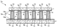
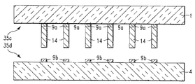
本発明は、第1の導電性パッドを含む第1の基板と、第2の導電性パッドを含む第2の基板と、第1の導電性パッドを第2の導電性パッドに電気的かつ機械的に接続する相互接続構造体とを備えた電気的構造体を提供する。ここで相互接続構造体は、無はんだ(non-solder)金属コア構造体と、無はんだ金属コア構造体の第1の部分と直接機械的に接触する第1のはんだ構造体と、無はんだ金属コア構造体の第2の部分と直接機械的に接触する第2のはんだ構造体とを含み、第1のはんだ構造体は、無はんだ金属コア構造体の第1の部分を第1の導電性パッドに電気的かつ機械的に接続し、第2のはんだ構造体は、無はんだ金属コア構造体の第2の部分を第2の導電性パッドに電気的かつ機械的に接続する。 The present invention relates to a first substrate including a first conductive pad, a second substrate including a second conductive pad, and electrically and mechanically connecting the first conductive pad to the second conductive pad. An electrical structure with an interconnecting interconnect structure is provided. Here, the interconnect structure includes a non-solder metal core structure, a first solder structure in direct mechanical contact with the first portion of the solderless metal core structure, and a solderless metal. A second solder structure in direct mechanical contact with the second portion of the core structure, the first solder structure comprising the first portion of the solderless metal core structure having a first conductivity. Electrically and mechanically connected to the pad, the second solder structure electrically and mechanically connects the second portion of the solderless metal core structure to the second conductive pad.
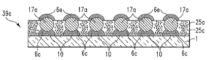
本発明は、第1の導電性パッドを含む第1の基板と、第2の導電性パッドを含む第2の基板と、第1の導電性パッドを第2の導電性パッドに電気的かつ機械的に接続する相互接続構造体とを備えた電気的構造体を提供するが、ここで相互接続構造体は、無はんだ金属コア構造体と、無はんだ金属コア構造体の全外表面を覆うはんだ層とを含み、全外表面は、第1の金属構造体を完全に取り囲み、はんだ層は、無はんだ金属コア構造体の全表面と直接に電気的かつ機械的に接触し、またはんだ層は、無はんだ金属コア構造体を第1の導電性パッド及び第2の導電性パッドに電気的かつ機械的に接続する。 The present invention relates to a first substrate including a first conductive pad, a second substrate including a second conductive pad, and electrically and mechanically connecting the first conductive pad to the second conductive pad. An electrical structure with interconnecting interconnect structures, wherein the interconnect structure includes a solderless metal core structure and a solder covering the entire outer surface of the solderless metal core structure And the outer surface completely surrounds the first metal structure, the solder layer is in direct electrical and mechanical contact with the entire surface of the solderless metal core structure, or the solder layer is The solderless metal core structure is electrically and mechanically connected to the first conductive pad and the second conductive pad.
本発明は、第1の導電性パッドを含む第1の基板と、第2の導電性パッドを含む第2の基板と、円筒形状を備えた無はんだ金属コア構造体を含むトランスファー(転移)膜とを準備するステップと、第1の導電性パッド上に第1のはんだ構造体を形成するステップと、第1のはんだ構造体を形成するステップの後で、無はんだ金属コア構造体の第1の側面が第1のはんだ構造体と接触するようにトランスファー膜を配置する第1の位置決めステップと、第1の位置決めステップの後で、第1のはんだ構造体を溶融させて無はんだ金属コア構造体の第1の側面と第1の導電性パッドとの間に電気的かつ機械的接続を形成するのに十分な温度まで無はんだ金属コア構造体を加熱する第1の加熱ステップと、第1の加熱ステップの後で、無はんだ金属コア構造体からトランスファー膜を除去するステップと、第2の導電性パッド上に第2のはんだ構造体を形成するステップと、第2のはんだ構造体を形成するステップの後で、無はんだ金属コア構造体の第2の側面が第2のはんだ構造体と接触するように、無はんだ金属コア構造体を含む第1の基板を配置する第2の位置決めステップと、第2の位置決めステップの後で、第2のはんだ構造体のはんだを溶融させ、無はんだ金属コア構造体の第2の側面と第2の導電性パッドとの間に電気的かつ機械的接続を形成するのに十分な温度まで無はんだ金属コア構造体を加熱して第1の導電性パッドと第2の導電性パッドとの間に電気的かつ機械的接続をもたらす第2の加熱ステップとを含む、電気的構造体を形成する方法を提供する。 The present invention relates to a transfer film including a first substrate including a first conductive pad, a second substrate including a second conductive pad, and a solderless metal core structure having a cylindrical shape. And after forming the first solder structure on the first conductive pad and forming the first solder structure, the first of the solderless metal core structure. A first positioning step in which the transfer film is disposed so that the side surface of the first solder structure is in contact with the first solder structure; and after the first positioning step, the first solder structure is melted to form a solderless metal core structure A first heating step for heating the solderless metal core structure to a temperature sufficient to form an electrical and mechanical connection between the first side of the body and the first conductive pad; After the heating step, solderless gold After removing the transfer film from the core structure, forming the second solder structure on the second conductive pad, and forming the second solder structure, the solderless metal core After the second positioning step, placing a first substrate comprising a solderless metal core structure such that the second side of the structure is in contact with the second solder structure; To a temperature sufficient to melt the solder of the second solder structure and form an electrical and mechanical connection between the second side of the solderless metal core structure and the second conductive pad Forming an electrical structure comprising heating a solderless metal core structure to provide an electrical and mechanical connection between the first conductive pad and the second conductive pad; Provide a way to do it.
本発明は、第1の導電性パッドを含む第1の基板と、第2の導電性パッドを含む第2の基板と、第1のキャビティを含む第1のトランスファー基板と、球形状を備え、第1のキャビティの直径よりも小さな直径を備える無はんだ金属コア構造体とを準備するステップと、第1の導電性パッド上に第1のはんだ構造体を形成するステップと、第1のトランスファー基板内の第1のキャビティ内に無はんだ金属コア構造体をディスペンス(分配)するステップと、ディスペンスするステップの後で、無はんだ金属コア構造体の表面の第1の部分が第1のはんだ構造体と接触するように、第1のトランスファー基板を配置する第1の位置決めステップと、第1の位置決めステップの後で、第1のはんだ構造体を溶融させて無はんだ金属コア構造体の表面の第1の部分と第1の導電性パッドとの間に電気的かつ機械的接続を形成するのに十分な温度まで無はんだ金属コア構造体を加熱する第1の加熱ステップと、第1の加熱ステップの後で、無はんだ金属コア構造体から第1のトランスファー基板を除去するステップと、第2の導電性パッド上に第2のはんだ構造体を形成するステップと、無はんだ金属コア構造体の表面の第2の部分が第2のはんだ構造体と接触するように無はんだ金属コア構造体を含む第1の基板を配置する第2の位置決めステップと、第2の位置決めステップの後に、第2のはんだ構造体を溶融させ、無はんだ金属コア構造体の表面の第2の部分と第2の導電性パッドとの間に電気的かつ機械的接続を形成するのに十分な温度まで無はんだ金属コア構造体を加熱して第1の導電性パッドと第2の導電性パッドとの間に電気的かつ機械的接続をもたらすステップとを含む、電気的構造体を形成する方法を提供する。 The present invention comprises a first substrate including a first conductive pad, a second substrate including a second conductive pad, a first transfer substrate including a first cavity, and a spherical shape, Providing a solderless metal core structure having a diameter smaller than the diameter of the first cavity; forming a first solder structure on the first conductive pad; and a first transfer substrate A first portion of the surface of the solderless metal core structure is the first solder structure after dispensing and dispensing the solderless metal core structure within the first cavity in the first cavity; A first positioning step of placing the first transfer substrate in contact with the first soldering substrate, and after the first positioning step, the first solder structure is melted to form a solderless metal core structure. A first heating step for heating the solderless metal core structure to a temperature sufficient to form an electrical and mechanical connection between the first portion of the surface and the first conductive pad; After the heating step, the step of removing the first transfer substrate from the solderless metal core structure, the step of forming the second solder structure on the second conductive pad, and the solderless metal core structure A second positioning step of placing a first substrate including a solderless metal core structure such that a second portion of the body surface is in contact with the second solder structure; and after the second positioning step, The second solder structure is melted and is not heated to a temperature sufficient to form an electrical and mechanical connection between the second portion of the surface of the solderless metal core structure and the second conductive pad. Heat the solder metal core structure Electrically and between the conductive pad and the second conductive pad and a step to provide a mechanical connection, a method of forming an electrical structure.
本発明は、第1の導電性パッドを含む第1の基板と、第2の導電性パッドを含む第2の基板と、第1のキャビティを含む第1のトランスファー基板と、球形状を備え、第1のキャビティの直径よりも小さな直径を備える第1の無はんだ金属コア構造体と、球形状を備え、第1のキャビティの直径よりも小さな直径を備える第2の無はんだ金属コア構造体とを準備するステップと、第1の導電性パッド上に第1のはんだ構造体を形成するステップと、第1のトランスファー基板内の第1のキャビティ内に第1の無はんだ金属コア構造体をディスペンスする第1のディスペンス・ステップと、第1のディスペンス・ステップの後で、第1の無はんだ金属コア構造体の表面の第1の部分が第1のはんだ構造体と接触するように第1のトランスファー基板を配置する第1の位置決めステップと、第1の位置決めステップの後で、第1のはんだ構造体を溶融させて第1の無はんだ金属コア構造体の表面の第1の部分と第1の導電性パッドとの間に電気的かつ機械的接続を形成するのに十分な温度まで第1の無はんだ金属コア構造体を加熱する第1の加熱ステップと、第1の加熱ステップの後に、無はんだ金属コア構造体から第1のトランスファー基板を除去するステップと、第1のアンダーフィル封止材料層を第1の基板に塗布するステップと、第1の無はんだ金属コア構造体の表面の第2の部分の上に第2のはんだ構造体を形成するステップと、第1のトランスファー基板内の第1のキャビティ内に第2の無はんだ金属コア構造体をディスペンスする第2のディスペンス・ステップと、第2のディスペンス・ステップの後で、第2の無はんだ金属コア構造体の表面の第1の部分が第2のはんだ構造体と接触するように第1のトランスファー基板を配置する第2の位置決めステップと、第2の位置決めステップの後で、第2のはんだ構造体を溶融させて第1の無はんだ金属コア構造体の表面の第2の部分と第2の無はんだ金属コア構造体の表面の第1の部分との間に電気的かつ機械的接続を形成するのに十分な温度まで第2の無はんだ金属コア構造体を加熱する第2の加熱ステップと、第2の加熱ステップの後で、第2の無はんだ金属コア構造体から、第2の無はんだ金属コア構造体の第1の部分及び第1のトランスファー基板を除去するステップと、第2の導電性パッド上に第3のはんだ構造体を形成するステップと、第2の無はんだ金属コア構造体の表面の第2の部分が第2のはんだ構造体と接触するように、第1の無はんだ金属コア構造体及び第2の無はんだ金属コア構造体を含む第1の基板を配置する第3の位置決めステップと、第3の位置決めステップの後で、第3のはんだ構造体のはんだを溶融させ、第2の無はんだ金属コア構造体の表面の第2の部分と第2の導電性パッドとの間に電気的かつ機械的接続を形成するのに十分な温度まで第2の無はんだ金属コア構造体を加熱して第1の導電性パッドと第2の導電性パッドとの間に電気的かつ機械的接続をもたらす第3の加熱ステップとを含む、電気的構造体を形成する方法を提供する。 The present invention comprises a first substrate including a first conductive pad, a second substrate including a second conductive pad, a first transfer substrate including a first cavity, and a spherical shape, A first solderless metal core structure having a diameter smaller than the diameter of the first cavity; a second solderless metal core structure having a spherical shape and having a diameter smaller than the diameter of the first cavity; Providing a first solder structure on the first conductive pad; dispensing a first solderless metal core structure in a first cavity in the first transfer substrate; First dispensing step, and after the first dispensing step, the first portion of the surface of the first solderless metal core structure is in contact with the first solder structure. transfer A first positioning step for placing the plate, and after the first positioning step, the first solder structure is melted to form a first portion on the surface of the first solderless metal core structure and the first A first heating step of heating the first solderless metal core structure to a temperature sufficient to form an electrical and mechanical connection with the conductive pad; and after the first heating step, Removing the first transfer substrate from the solder metal core structure; applying a first underfill encapsulant layer to the first substrate; and a first surface of the first solderless metal core structure. Forming a second solder structure on the two portions, and a second dispensing step of dispensing a second solderless metal core structure in a first cavity in the first transfer substrate; The second After the dispensing step, a second positioning step of positioning the first transfer substrate such that the first portion of the surface of the second solderless metal core structure is in contact with the second solder structure; After the second positioning step, the second solder structure is melted to cause the second portion of the surface of the first solderless metal core structure and the first of the surface of the second solderless metal core structure. A second heating step of heating the second solderless metal core structure to a temperature sufficient to form an electrical and mechanical connection with the portion of the second portion, and after the second heating step, Removing the first portion of the second solderless metal core structure and the first transfer substrate from the second solderless metal core structure, and a third solder structure on the second conductive pad Forming a second and no second A first substrate comprising a first solderless metal core structure and a second solderless metal core structure such that a second portion of the surface of the metal core structure is in contact with the second solder structure After the third positioning step, the solder of the third solder structure is melted, the second portion of the surface of the second solderless metal core structure and the second Heating the second solderless metal core structure to a temperature sufficient to form an electrical and mechanical connection between the first conductive pad and the second conductive pad; And a third heating step that provides an electrical and mechanical connection between them.
本発明は、第1の導電性パッド及び第2の導電性パッドを含む第1の基板と、第3の導電性パッド及び第4の導電性パッドを含む第2の基板と、第1のキャビティ及び第2のキャビティを含む第1のトランスファー基板と、球形状を備え、第1のキャビティの直径よりも小さな直径を備える無はんだ金属コア構造体とを準備するステップと、第1の導電性パッド上に第1のはんだ構造体を形成するステップと、第2の導電性パッド上に第2のはんだ構造体を形成するステップと、第1のキャビティに対応する開口部を有する膜で第2のキャビティを覆うステップと、第1のトランスファー基板内の第1のキャビティ内に無はんだ金属コア構造体をディスペンスするステップと、無はんだ金属コア構造体の表面の第1の部分が第1のはんだ構造体に接触し、かつ、第2のキャビティが第2のはんだ構造体に位置合せされるように第1のトランスファー基板を配置する第1の位置決めステップと、第1のはんだ構造体を溶融させて無はんだ金属コア構造体の表面の第1の部分と第1の導電性パッドとの間に電気的かつ機械的接続を形成するのに十分な温度まで無はんだ金属コア構造体を加熱する第1の加熱ステップと、無はんだ金属コア構造体から第1のトランスファー基板を除去するステップと、第3の導電性パッド上に第3のはんだ構造体を形成するステップと、第4の導電性パッド上に第4のはんだ構造体を形成するステップと、無はんだ金属コア構造体の表面の第2の部分が第3のはんだ構造体と接触し、かつ、第2のはんだ構造体が第4のはんだ構造体と接触するように無はんだ金属コア構造体を含む第1の基板を配置する第2の位置決めステップと、第3のはんだ構造体のはんだを溶融させ、無はんだ金属コア構造体の表面の第2の部分と第3の導電性パッドとの間に電気的かつ機械的接続を形成するのに十分な温度まで無はんだ金属コア構造体を加熱して第1の導電性パッドと第3の導電性パッドとの間に電気的かつ機械的接続をもたらす第2の加熱ステップと、第2のはんだ構造体及び第4のはんだ構造体を溶融させ、第2のはんだ構造体と第4のはんだ構造体との間に電気的かつ機械的接続を形成するのに十分な温度まで第2のはんだ構造体及び第4のはんだ構造体を加熱して第2の導電性パッドと第4の導電性パッドとの間に電気的かつ機械的接続をもたらす第3の加熱ステップであって、第2の加熱ステップと同時に実行される第3の加熱ステップとを含む電気的構造体を形成する方法を提供する。 The present invention includes a first substrate including a first conductive pad and a second conductive pad, a second substrate including a third conductive pad and a fourth conductive pad, and a first cavity. And a first transfer substrate including a second cavity, a solderless metal core structure having a spherical shape and having a diameter smaller than the diameter of the first cavity, and a first conductive pad Forming a second solder structure on the second conductive pad; forming a second solder structure on the second conductive pad; and forming a second solder film with an opening corresponding to the first cavity. Covering the cavity; dispensing the solderless metal core structure into the first cavity in the first transfer substrate; and a first portion of the surface of the solderless metal core structure is the first solder structure. And a first positioning step in which the first transfer board is disposed so that the second cavity is aligned with the second solder structure, and the first solder structure is melted to A first heating the solderless metal core structure to a temperature sufficient to form an electrical and mechanical connection between the first portion of the surface of the solder metal core structure and the first conductive pad. Heating, removing the first transfer substrate from the solderless metal core structure, forming a third solder structure on the third conductive pad, and on the fourth conductive pad Forming a fourth solder structure; a second portion of the surface of the solderless metal core structure is in contact with the third solder structure; and the second solder structure is the fourth solder structure. No need to touch the body A second positioning step of disposing a first substrate including a metal core structure, melting the solder of the third solder structure, and a second portion of the surface of the solderless metal core structure with a third The solderless metal core structure is heated to a temperature sufficient to form an electrical and mechanical connection with the conductive pad to provide an electrical connection between the first conductive pad and the third conductive pad. A second heating step for providing a mechanical and mechanical connection, melting the second solder structure and the fourth solder structure, and electrically connecting the second solder structure and the fourth solder structure. And heating the second solder structure and the fourth solder structure to a temperature sufficient to form a mechanical connection to electrically and between the second conductive pad and the fourth conductive pad. A third heating step for providing a mechanical connection, wherein the second heating step And a third heating step performed simultaneously with the step of forming the electrical structure.
本発明は、有益なことに、構造体間の接続部を形成するための簡単な構造体及び関連する方法を提供する。 The present invention beneficially provides a simple structure and associated method for forming connections between structures.
図1は、本発明の実施形態による電気的構造体2aの断面図を示す。電気的構造体2aは、基板1と、基板4と、複数の相互接続構造体5aとを含む。基板1は、複数の導電性パッド10を含む。導電性パッド10の各々のパッドは、基板1内の配線又は電気的コンポーネントに接続することができる。基板4は、複数の導電性パッド12を含む。導電性パッド12の各々のパッドは、基板4内の配線又は電気的コンポーネントに接続することができる。基板1は、とりわけ、半導体デバイス(例えば、集積回路チップ、半導体ウェハ等)、チップ・キャリア(有機物又は無機物)、プリント回路基板等を含むことができる。基板4は、とりわけ、半導体デバイス(例えば、集積回路チップ、半導体ウェハ等)、チップ・キャリア(有機物又は無機物)、プリント回路基板等を含むことができる。各々の相互接続構造体5aは、無はんだ金属(即ち、はんだ材料を含まない)コア構造体14と、はんだ構造体6aとを含む。はんだ構造体6aは、はんだを含む。はんだは、本明細書においては、金属表面を溶融させることなく金属表面を互いに接合するのに用いられる低融点(即ち、摂氏約100度から摂氏約340度まで)を備えた金属合金と定義する。はんだ構造体6aは、無はんだ金属コア構造体14を完全に取り囲むはんだ層を含む。代替的に(即ち、無はんだ金属コア構造体14を完全に取り囲むはんだ層の代りに)、はんだ構造体6aは、無はんだ金属コア構造体14の上面14aに結合された第1のはんだ部分9aと、無はんだ金属コア構造体14の底面14bに結合された第2のはんだ部分9bとを含むことができる。各々の無はんだ金属コア構造体14は、とりわけ、銅、金、ニッケル等を含む、はんだを含まない何れかの導電性金属材料を含むことができる。各々の相互接続構造体5aは、導電性パッド10を導電性パッド12に電気的かつ機械的に接続する。無はんだ金属コア構造体14は円筒形状を備える。はんだ構造体6aは、とりわけ、SnCu、SnAgCu、SnPb等のようなスズの合金を含む、フリップ・チップ相互接続に適した何れかのはんだ材料を含むことができる。
FIG. 1 shows a cross-sectional view of an electrical structure 2a according to an embodiment of the present invention. The electrical structure 2a includes a
図2は、図1の第1の代替物を図示し、本発明の実施形態による電気的構造体2bの断面図を示す。電気的構造体2bは、基板1と、基板4と、複数の相互接続構造体5bとを含む。図1の電気的構造体2aと対比すると、図2の電気的構造体2bは、複数の相互接続構造体5bを含む。相互接続構造体5bの各々は、球形の無はんだ(即ち、はんだ材料を含まない)金属コア構造体17と、はんだ構造体6bとを含む。各々のはんだ構造体6bは、対応する無はんだ金属コア構造体17を完全に取り囲むはんだ層を含む。さらに、相互接続構造体5bの各々は、付加的なはんだ構造体6dを含むことができる。各々のはんだ構造体6bは、対応する無はんだ金属コア構造体17を対応する導電性パッド10に電気的かつ機械的に接続する。各々のはんだ構造体6dは、対応する無はんだ金属コア構造体17を(即ち、はんだ構造体6bを通して)対応する導電性パッド12に電気的かつ機械的に接続する。上述の接続は、導電性パッド10を対応する導電性パッド12に電気的かつ機械的に接続する各々の相互接続構造体5bをもたらす。随意的に、2つの異なるタイプのはんだ材料をはんだ構造体6b及びはんだ構造体6dに用いることができる。例えば、はんだ構造体6bは、AuSnはんだ材料を含むことができ、はんだ構造体6dは、とりわけ、SnAg、SnCu、SnAgCu、SnBi等のようなはんだ材料を含むことができる。第1のレベル領域のアレイ相互接続部に対しては、各々の無はんだ金属コア構造体17は、約25ミクロン乃至約150ミクロンの直径を備えることができる。第2のレベル領域のアレイ相互接続部(例えば、ボール・グリッド・アレイ(BGA))に対しては、各々の無はんだ金属コア構造体17は、約0.2mm乃至約1.5mmの直径を備えることができる。各々の無はんだ金属コア構造体17は、とりわけ、銅、金、ニッケル等を含む、はんだを含まない何れかの導電性金属材料のコアを含むことができる。さらに、各々の無はんだ金属コア構造体17は、無はんだ金属コア構造体17を取り囲む(例えば、下記の図3の層19を参照)無はんだ金属材料(即ち、無はんだ金属コア構造体17に含まれる材料とは異なる)の付加的な層を含むことができる。付加的な層は、とりわけ、ニッケル、金、スズ等を含む何れかの導電性金属材料を含むことができる。
FIG. 2 illustrates the first alternative of FIG. 1 and shows a cross-sectional view of an
図3は、図2の第1の代替物を図示し、本発明の実施形態による電気的構造体2cの断面図を示す。電気的構造体2cは、基板1と、基板4と、複数の相互接続構造体5cとを含む。図2の電気的構造体2bと対比すると、図3の電気的構造体2cは、複数の相互接続構造体5cを含む。相互接続構造体5cの各々は、無はんだ金属コア構造体17と、はんだ構造体6cと、はんだ構造体6dとを含む。各々のはんだ構造体6cは、対応する無はんだ金属コア構造体17を対応する導電性パッド10に電気的かつ機械的に接続する。各々のはんだ構造体6dは、対応する無はんだ金属コア構造体17を対応する導電性パッド12に電気的かつ機械的に接続する。上述の接続は、導電性パッド10を対応する導電性パッド12に電気的かつ機械的に接続する各々の相互接続構造体5cをもたらす。随意的に、2つの異なるタイプのはんだ材料をはんだ構造体6c及びはんだ構造体6dに用いることができる。例えば、はんだ構造体6cはAuSnはんだ材料を含むことができ、はんだ構造体6dは、とりわけ、SnAg、SnCu、SnAgCu、SnBi等のようなはんだ材料を含むことができる。各々の無はんだ金属コア構造体17は、とりわけ、銅、金、ニッケル等を含む、はんだを含まない何れかの導電性金属材料のコアを含むことができる。さらに、各々の無はんだ金属コア構造体17は、無はんだ金属コア構造体17を取り囲む無はんだ金属材料の(即ち、無はんだ金属コア構造体17に含まれる材料とは異なる)付加的な層19を含むことができる。付加的な層19は、とりわけ、ニッケル、金、スズ等を含む何れかの導電性金属材料を含むことができる。
FIG. 3 illustrates the first alternative of FIG. 2 and shows a cross-sectional view of an electrical structure 2c according to an embodiment of the present invention. The electrical structure 2c includes a
図4は、図3の第1の代替物を図示し、本発明の実施形態による電気的構造体2dの断面図を示す。電気的構造体2dは、基板1と、基板4と、複数の相互接続構造体5dとを含む。図3の電気的構造体2cと対比すると、図4の電気的構造体2dは、複数の相互接続構造体5dを含む。相互接続構造体5dの各々は、無はんだ金属コア構造体17aと、無はんだ金属コア構造体17bと、はんだ構造体6cと、はんだ構造体6dと、はんだ構造体6eとを含む。これに加えて(即ち、随意的に)、電気的構造体2dは、アンダーフィル封止材料層25aと、アンダーフィル封止材料層25bとを含む。各々のはんだ構造体6eは、無はんだ金属コア構造体17aを対応する無はんだ金属コア構造体17bに電気的かつ機械的に接続する。各々のはんだ構造体6cは、無はんだ金属コア構造体17aを対応する導電性パッド10に電気的かつ機械的に接続する。各々のはんだ構造体6dは、無はんだ金属コア構造体17bを対応する導電性パッド12に電気的かつ機械的に接続する。上述の接続は、導電性パッド10を対応する導電性パッド12に電気的かつ機械的に接続する各々の相互接続構造体5dをもたらす。随意的に、3つの異なるタイプのはんだ材料をはんだ構造体6c、はんだ構造体6d及びはんだ構造体6eに用いることができる。例えば、はんだ構造体6cはAuSnのはんだ材料を含むことができ、はんだ構造体6dは、とりわけ、SnAg、SnCu等のようなはんだ材料を含むことができ、はんだ構造体6eは、とりわけ、SnAgCu、SnBi等のようなはんだ材料を含むことができる。各々の無はんだ金属コア構造体17a及び17bは、とりわけ、銅、金、ニッケル等を含む、はんだを含まない何れかの導電性金属材料のコアを含むことができる。無はんだ金属コア構造体17aは第1の材料(例えば、銅)を含むことができ、無はんだ金属コア構造体17bは第2の材料(例えば、金)を含むことができる。さらに、各々の無はんだ金属コア構造体17a及び17bは、無はんだ金属コア構造体17a及び17bを取り囲む金属材料の(即ち、無はんだ金属コア構造体17a及び17bに含まれる材料とは異なる)付加的な層19を含むことができる。付加的な層19は、とりわけ、ニッケル、金、スズ等を含む何れかの導電性金属材料を含むことができる。さらに、無はんだ金属コア構造体17aは、無はんだ金属コア構造体17b上の層19とは異なる材料を含む層19を含むことができる。アンダーフィル封止材料層25aは、無はんだ金属コア構造体17aを取り囲み、基板1と接触する。アンダーフィル封止材料層25bは、無はんだ金属コア構造体17bを取り囲み、基板4と接触する。アンダーフィル封止材料層25aは、アンダーフィル封止材料層25bと接触する。アンダーフィル封止材料層25aは、第1の材料(例えば、高度に充填されたシリカ・エポキシ複合接着剤)を含むことができ、アンダーフィル封止材料層25bは、第2の異なる材料(例えば、軽度に充填されたシリカ・エポキシ複合接着剤)を含むことができる。アンダーフィル封止材料層25aは、カプセル材料層25bが有する第2の熱膨張係数(例えば、約15.1−40ppm/Cの範囲を含む)とは異なる(例えば、より小さな)第1の熱膨張係数(例えば、約5−15ppm/Cの範囲を含む)を有することができる。アンダーフィル封止材料層25aは、さらに、全域に分散したフィラー25cを含むことができる。
FIG. 4 illustrates the first alternative of FIG. 3 and shows a cross-sectional view of an electrical structure 2d according to an embodiment of the present invention. The electrical structure 2d includes a
図5は、本発明の実施形態による電気的構造体2eの断面図を示す。図5の電気的構造体2eは、図2及び図3の電気的構造体2b及び2cの組合せである。図2及び図3の電気的構造体2b及び2cに加えて、図5の電気的構造体2eは、導電性パッド10の幾つかを対応する導電性パッド12に電気的かつ機械的に接続する相互接続構造体29(即ち、はんだを含む)を含む。従って、電気的構造体2eは、相互接続構造体5b、5c及び29の組合せを用いて、導電性パッド10を対応する導電性パッド12に電気的かつ機械的に接続する。相互接続構造体5b、5c及び29の任意の組合せ及び任意の構成を用いて、導電性パッド10を対応する導電性パッド12に電気的かつ機械的に接続することができることに留意されたい。例えば、電気的構造体2eは、導電性パッド10を対応する導電性パッド12に電気的かつ機械的に接続するために相互接続構造体5c及び29のみを備えることができる。任意の数又は割合の相互接続構造体5b、5c及び29を任意のパターンに配置することができる(例えば、相互接続構造体5b及び29は、それらが交互配置されるように配置することができ、ランダムな位置に配置することができ、3つの相互接続構造体29毎に1つの相互接続構造体5bが存在するように配置することができ、相互接続構造体5bは電力及び接地接続のみをもたらし、かつ、相互接続構造体29は信号相互接続用にのみ配置することができる等)。さらに、電気的構造体2eは、基板1と基板4の間にアンダーフィル封止材料層31を含むことができる。
FIG. 5 shows a cross-sectional view of an
図6は、図2の第2の代替物を図示し、本発明の実施形態による電気的構造体2fの断面図を示す。図2の電気的構造体2bと対比すると、図6の電気的構造体2fは、基板1と基板4の間にアンダーフィル封止材料層32aを含む。基板1が半導体デバイス又はシリコン・ウェハである場合には、アンダーフィル封止材料層32aは、代替的に、チップ接合の前に塗布されるか又は相互接続構造体5bを覆ってシリコン・ウェハ上に塗布されるアンダーフィル層を含むことができる。このようなアンダーフィル層は、ウェハ・レベルのアンダーフィルと定義される。
FIG. 6 illustrates the second alternative of FIG. 2 and shows a cross-sectional view of an electrical structure 2f according to an embodiment of the present invention. In contrast to the
図7は、図1の第2の代替物を図示し、本発明の実施形態による電気的構造体2gの断面図を示す。図1の電気的構造体2aと対比すると、図7の電気的構造体2gは、基板1と基板4の間にアンダーフィル封止材料層32bを含む。基板1が半導体デバイス又はシリコン・ウェハである場合には、アンダーフィル封止材料層32bは、代替的に、チップ接合の前に塗布されるか又は相互接続構造体5a上のシリコン・ウェハ上に塗布されるアンダーフィル層を含むことができる。このようなアンダーフィル層は、ウェハ・レベルのアンダーフィルと定義される。
FIG. 7 illustrates the second alternative of FIG. 1 and shows a cross-sectional view of an electrical structure 2g according to an embodiment of the present invention. In contrast to the electrical structure 2 a in FIG. 1, the electrical structure 2 g in FIG. 7 includes an underfill
図8は、図3の第2の代替物を図示し、本発明の実施形態による電気的構造体2hの断面図を示す。図3の電気的構造体2cと対比すると、図8の電気的構造体2hは、基板1と基板4の間にアンダーフィル封止材料層32cを含む。基板1が半導体デバイス又はシリコン・ウェハである場合には、アンダーフィル封止材料層32cは、代替的に、チップ接合の前に塗布されるか又は相互接続構造体5cを覆ってシリコン・ウェハ上に塗布されるアンダーフィル層を含むことができる。このようなアンダーフィル層は、ウェハ・レベルのアンダーフィルと定義される。
FIG. 8 illustrates the second alternative of FIG. 3 and shows a cross-sectional view of an
図9乃至図15は、本発明の実施形態による、図1の電気的構造体2aを形成するプロセスを示す。 9-15 illustrate a process for forming the electrical structure 2a of FIG. 1 according to an embodiment of the present invention.
図9は、本発明に実施形態による、絶縁体層35の上に形成された無はんだ金属層37の断面図を示す。無はんだ金属層37は、とりわけ、銅、金、ニッケル等のような何れかの無はんだ金属材料を含むことができる。絶縁体層35は、とりわけ、ポリマー膜(例えば、ポリイミド)等のような何れかの絶縁体材料を含むことができる。
FIG. 9 shows a cross-sectional view of a
図10は、本発明に実施形態による、構造体35aを形成するために無はんだ金属相互接続構造体14を形成した後の図9の構造体の断面図を示す。無はんだ金属相互接続構造体14は、無はんだ金属相互接続構造体14(即ち、図1の)を形成するように無はんだ金属層37の部分を減法エッチングすることによって形成することができる。無はんだ金属相互接続構造体14は、種々の幅、高さ及び高さ対幅のアスペクト比を備えることができる。減法エッチング・プロセスは、
1.保護フォトレジスト層を塗布し、パターン形成するステップと、
2.化学溶液を用いて、銅の非保護領域をエッチング又は溶解するステップと、
3.保護フォトレジスト層を剥離するステップと
を含む。
FIG. 10 shows a cross-sectional view of the structure of FIG. 9 after forming the solderless
1. Applying and patterning a protective photoresist layer; and
2. Etching or dissolving the unprotected areas of copper using a chemical solution;
3. Stripping the protective photoresist layer.
無はんだ金属相互接続構造体14の各々は、約10ミクロン乃至約100ミクロンの幅を備え、約1:1乃至約5:1の高さ対幅のアスペクト比を備えることができる。
Each of the solderless
図11は、本発明の実施形態による、第1のはんだ部分9a(即ち、はんだ構造体)を形成して構造体35bを形成した後の図1の基板1の断面図を示す。例えば、基板1は、導電性相互接続パッド(例えば、図1のパッド10を参照)を備えたシリコン・デバイス・ウェハを含むことができる。はんだをパッドに塗布して、第1のはんだ部分9aを形成する。はんだを導電性相互接続パッドに塗布するのに、とりわけ、射出成形はんだとしてはんだを塗布することを含む任意の方法を用いることができる。
FIG. 11 shows a cross-sectional view of the
図12は、本発明の実施形態による図1において、図11の構造体35bと位置合せされた、図10の構造体35aの断面図を示す。無はんだ金属相互接続構造体14は、対応する第1のはんだ部分9aに位置合せされる。位置合せプロセスは、基板1及び絶縁体層35上の基準点の光検出を用いる市販の接合ツールを用いるステップを含むことができる。
12 shows a cross-sectional view of the structure 35a of FIG. 10 aligned with the
図13は、本発明の実施形態による、図12に関して説明した位置合せプロセスの後に形成された構造体35cの断面図を示す。図13において、トランスファー(転移)プロセスは、図12の位置合せされた組立体を、第1のはんだ部分9aを形成するのに用いたはんだの融点より高い温度に加熱することによって(即ち、フラックス剤又はフラックス雰囲気の助けにより)実行することができる。随意的に、トランスファー・プロセスは、絶縁体層35の裏面21を通して適用されるレーザ放出プロセスによって支援することができる。レーザによって発生された光エネルギーは、絶縁体層35により無はんだ金属相互接続構造体14との界面23において吸収され、接着力(すなわち、界面23における)を低下させて絶縁体層35から無はんだ金属相互接続構造体14を解放する。代替的に、上述のはんだ溶融プロセス中に接着剤(すなわち、界面23における)を劣化させて絶縁体層35から無はんだ金属相互接続構造体14を解放することができる。
FIG. 13 illustrates a cross-sectional view of a
図14は、本発明の実施形態による、図13の構造体35cを構造体35dに位置合せするプロセスの断面図を示す。構造体35dは、形成されたはんだ構造体9b(即ち、図11に関して実行されたプロセスと同様のプロセスによって形成された)を含んだ基板4を含む。
FIG. 14 illustrates a cross-sectional view of a process for aligning the
図15は、本発明の実施形態による、図1の電気的構造体2aに類似の完成した電気的構造体35eを示す。基板1から基板4までの、無はんだ金属相互接続構造体14、はんだ構造体9a、及びはんだ構造体9bを通した組立ては、フラックス剤又はフラックス雰囲気の助けにより、無はんだ金属相互接続構造体14の温度をはんだ構造体9bの溶融温度よりも高くすることによって行われる。随意的に、無はんだ金属相互接続構造体14、はんだ構造体9a、及びはんだ構造体9bは、基板1を基板4に接合した後にキャピラリ・アンダーフィルによってポリマー材料で封止することができる。代替的に、アンダーフィル封止材料は、基板1を基板4に接合する前にウェハ・レベルで又は個別化したデバイスに塗布することができる。
FIG. 15 shows a completed
図16乃至図24は、本発明の実施形態による、図2の電気的構造体2b、図3の電気的構造体2c、及び図5の電気的構造体2eを形成するプロセスを示す。図16乃至図24は射出成形はんだとして、はんだを塗布するプロセスを示すが、任意のはんだ塗布プロセスを用いることができることに留意されたい。
FIGS. 16-24 illustrate a process for forming the
図16は、本発明の実施形態による、基板1(即ち、図2及び図3からの)上に配置された充填ガラス又はシリコン・モールド40を含む構造体39aの断面図を示す。ガラス又はシリコン・モールド40は、ガラス・モールドから解放されるときに、図2のはんだ構造体6b、図3のはんだ構造体6c、及び図5のはんだ構造体6bとなるはんだで充填される。はんだは、とりわけ、AuSn、SnCu、SnAgCu等のような、とりわけ、スズの合金を含む、フリップ・チップ相互接続に適した何れかのはんだを含むことができる。はんだは、はんだ構造体6b、6cが次のステップ中に溶融しないように高い融点を備えることができる。
FIG. 16 shows a cross-sectional view of a
図17は、本発明の実施形態による、図16の構造体39aから形成された構造体39bの断面図を示す。図17において、はんだはガラス又はシリコン・モールド40から解放されて基板1上の導電性パッド10に結合されたはんだ構造体6cを形成する。
FIG. 17 shows a cross-sectional view of a
図18は、本発明の実施形態による、複数の無はんだ金属コア構造体17を含むトランスファー基板43の断面図を示す。無はんだ金属コア構造体17は、トランスファー基板43内のキャビティ43a内に配置される。キャビティ43aの各々は、導電性パッド10上の対応するはんだ構造体6cの位置に対応するキャビティ位置を有する無はんだ金属コア構造体17と類似の寸法を備える。トランスファー基板43は、とりわけ、ガラス、シリコン、又は射出成形はんだモールド等に用いられる何れかの材料を含むことができる。無はんだ金属コア構造体17は、とりわけ、水、アルコール(例えば、イソプロパノール)等のような溶剤中のスラリーとしてキャビティ43a内にディスペンスすることができる。溶剤は、はんだ構造体6cの無はんだ金属コア構造体17への濡れを補助するように適切な量のフラックスを含むことができる。無はんだ金属コア構造体17が金でコーティングされる場合には、フラックスは不要である。随意的に、溶剤はさらに、無はんだ金属コア構造体17をキャビティ43a内に保持するのを補助する少量の熱分解性ポリマー接着剤を含むことができる。キャビティ43aは、無はんだ金属コア構造体17のディスペンス中に、1つの無はんだ金属コア構造体17だけをその中に入れるサイズに形成される。
FIG. 18 shows a cross-sectional view of a
図19は、本発明の実施形態による、選択された複数の無はんだ金属コア構造体17を含む、図18のトランスファー基板43の断面図を示す。プロセスの随意的な特徴として、トランスファー基板43は、キャビティ43aのある所定部分と適合する貫通孔を有するポリマー膜(図示せず)で覆うことができる。ポリマー膜で覆われたキャビティ43aの所定部分は、無はんだ金属コア構造体17の受取りを妨げられることになる。キャビティ43aの所定部分は、パッケージ化設計技術者が無はんだ金属コア構造体17を選択的に配置することを可能にする。さらに、はんだ相互接続部29は、基板1上への配置のために幾つかのキャビティ43a内に選択的に配置する(即ち、無はんだ金属コア構造体17を選択する代りに)ことができる。この選択肢においては、トランスファー基板43は、残りのキャビティ43aと適合する貫通孔を有する第2のポリマー膜(図示せず)で覆うことができる。ポリマー膜で覆われたキャビティ43aは、はんだ相互接続部29の受取りを妨げられることになる。
FIG. 19 illustrates a cross-sectional view of the
図20は、本発明の実施形態による、無はんだ金属コア構造体17を含むトランスファー基板43上に配置された、図17の基板1の断面図を示す。図17の基板1は、無はんだ金属コア構造体17を基板1に転写させるために、無はんだ金属コア構造体17を含むトランスファー基板43の上に配置される。
FIG. 20 shows a cross-sectional view of the
図21は、本発明の実施形態による、無はんだ金属コア構造体17がトランスファー基板43から解放され、はんだ構造体6bに接続された後の基板1の断面図を示す。図21において、はんだ構造体6bは、無はんだ金属コア構造体17を完全に取り囲む。
FIG. 21 shows a cross-sectional view of the
図22は、図21の代替物を示し、本発明の実施形態による、無はんだ金属コア構造体17がトランスファー基板43から解放され、はんだ構造体6cに接続された後の基板1を含む構造体39cの断面図を示す。図22において、はんだ構造体6cは、無はんだ金属コア構造体17を部分的に取り囲む。
FIG. 22 shows an alternative to FIG. 21, and the structure comprising the
図23は、本発明の実施形態による、基板4上に配置された基板1の断面図を示す。基板1は基板4に接続されて図2の電気的構造体2bを形成する。
FIG. 23 shows a cross-sectional view of a
図24は、本発明の実施形態による、基板4上に配置された基板1の代替的な断面図を示す。図19の選択肢が用いられる(即ち、はんだ相互接続構造体29を含む)場合には、配置(図示せず)は、図24における場合と同様に行われる。基板1は基板4に接続されて図3の電気的構造体2cを形成する。
FIG. 24 shows an alternative cross-sectional view of the
図25乃至図30は、本発明の実施形態による、図4の電気的構造体2dを形成するプロセスを示す。 FIGS. 25-30 illustrate a process of forming the electrical structure 2d of FIG. 4 according to an embodiment of the present invention.
図25は、本発明の実施形態による、アンダーフィル層25aを含む、図22の構造体39cを示す。図25の基板39cは、図16乃至図20を参照して説明したプロセス・ステップによって形成される。アンダーフィル層25aは、小さい熱膨張係数(CTE)を生成するようにフィラー25cを含むことができる。アンダーフィル層25aは、基板1のものと同様の熱膨張係数(CTE)を備えることができる。
FIG. 25 illustrates the
図26は、本発明の実施形態による、無はんだ金属コア構造体17a上に配置されたガラス又はシリコン・モールド40bを含む構造体39cを示す。ガラス又はシリコン・モールド40bは、モールド40bから解放されるときに、図4のはんだ構造体6eとなるはんだで充填される。はんだは、とりわけ、AuSn、SnCu、SnAgCu等のような、スズの合金を含む、フリップ・チップ相互接続に適した何れかのはんだを含むことができる。はんだは、はんだ構造体6eが次のステップ中に溶融しないように高融点を備えることができる。
FIG. 26 illustrates a
図27は、本発明の実施形態による、無はんだ金属コア構造体17aに結合されたはんだ構造体6eを含む構造体39cの断面図を示す。図27において、はんだは、ガラス又はシリコン・モールド40bから解放されて、無はんだ金属コア構造体17aに結合されたはんだ構造体6eを形成する。
FIG. 27 illustrates a cross-sectional view of a
図28は、本発明の実施形態による、無はんだ金属コア構造体17bを含むトランスファー基板43上に配置された、図27の構造体39cの断面図を示す。図27の構造体39cは、無はんだ金属コア構造体17bを転写させて無はんだ金属コア構造体17aに接続するように、無はんだ金属コア構造体17bを含むトランスファー基板43上に配置される。
FIG. 28 shows a cross-sectional view of
図29は、本発明の実施形態による、無はんだ金属コア構造体17bが無はんだ金属コア構造体17aに接続された後の図28の構造体39cの断面図を示す。
FIG. 29 shows a cross-sectional view of
図30は、本発明の実施形態による、アンダーフィル層25a上に塗布されたアンダーフィル層25bを含む、図29の構造体39cの断面図を示す。アンダーフィル層25bがアンダーフィル層25a上に塗布された後に、基板1は基板4に接続されて図4の電気的構造体2dを形成する。
FIG. 30 illustrates a cross-sectional view of the
本明細書において本発明の実施形態を例証のために説明したが、当業者であれば、多くの修正及び変更が明らかとなるであろう。従って、添付の特許請求の範囲は、全てのそのような修正及び変更を本発明の範囲内に含まれるものとして包含することが意図されている。 While embodiments of the present invention have been described herein for purposes of illustration, many modifications and changes will become apparent to those skilled in the art. Accordingly, the appended claims are intended to cover all such modifications and changes as fall within the scope of the invention.
1、4:基板
2a、2b、2c、2d、2e、2f、2g,2h:電気的構造体
5a、5b、5c、5d、29:相互接続構造体
6a、6b、6c、6d、6e:はんだ構造体
9a:第1のはんだ部分(はんだ構造体)
9b:第2のはんだ部分(はんだ構造体)
10、12:導電性パッド
14:無はんだ金属コア構造体(無はんだ金属相互接続構造体)
14a:無はんだ金属コア構造体14の上面
17、17a、17b:球状無はんだ金属コア構造体
19:付加層
21:絶縁体層35の裏面
23:界面
25a、25b、31、32a、32b、32c:アンダーフィル封止材料層
25c:フィラー
35:絶縁体層
35a、35b、35c、35d、39a、39b、39c:構造体
37:無はんだ金属層
40、40b:ガラス又はシリコン・モールド
43:トランスファー基板
43a:キャビティ
1, 4:
9b: Second solder portion (solder structure)
10, 12: Conductive pad 14: Solderless metal core structure (solderless metal interconnect structure)
14a:
Claims (5)
第2の導電性パッドを含む第2の基板と、
前記第1の導電性パッドを前記第2の導電性パッドに電気的かつ機械的に接続する相互接続構造体と
を含み、
前記相互接続構造体は、無はんだ金属コア構造体と、前記無はんだ金属コア構造体の第1の部分と直接機械的に接触する第1のはんだ構造体と、前記無はんだ金属コア構造体の第2の部分と直接機械的に接触する第2のはんだ構造体とを含み、
前記第1のはんだ構造体は、前記無はんだ金属コア構造体の前記第1の部分を前記第1の導電性パッドに電気的かつ機械的に接続し、
前記第2のはんだ構造体は、前記無はんだ金属コア構造体の前記第2の部分を前記第2の導電性パッドに電気的かつ機械的に接続し、
前記相互接続構造体は第3のはんだ構造体を含み、
前記無はんだ金属コア構造体は、球形状を備える第1の無はんだ金属コアと、前記球形状を備える第2の無はんだ金属コアとを含み、
前記第3のはんだ構造体は、前記第1の無はんだ金属コアを前記第2の無はんだ金属コアに電気的かつ機械的に結合させ、
前記無はんだ金属コア構造体の前記第1の部分は、前記第1の無はんだ金属コア上に配置され、
前記無はんだ金属コア構造体の前記第2の部分は、前記第2の無はんだ金属コア上に配置され、
前記第1のはんだ構造体は第1のはんだ材料を含み、
前記第2のはんだ構造体は第2のはんだ材料を含み、
前記第3のはんだ構造体は第3のはんだ材料を含み、
前記第1のはんだ材料は、前記第2のはんだ材料とは異なり、前記第3のはんだ材料は、前記第1のはんだ材料および前記第2のはんだ材料とは異なる、
電気的構造体。A first substrate including a first conductive pad;
A second substrate including a second conductive pad;
An interconnect structure for electrically and mechanically connecting the first conductive pad to the second conductive pad;
The interconnect structure includes a solderless metal core structure, a first solder structure in direct mechanical contact with the first portion of the solderless metal core structure, and the solderless metal core structure. A second solder structure in direct mechanical contact with the second portion;
The first solder structure electrically and mechanically connects the first portion of the solderless metal core structure to the first conductive pad;
The second solder structure electrically and mechanically connects the second portion of the solderless metal core structure to the second conductive pad;
The interconnect structure includes a third solder structure;
The solderless metal core structure includes a first solderless metal core having a spherical shape, and a second solderless metal core having the spherical shape,
The third solder structure electrically and mechanically couples the first solderless metal core to the second solderless metal core;
The first portion of the solderless metal core structure is disposed on the first solderless metal core;
The second portion of the solderless metal core structure is disposed on the second solderless metal core;
The first solder structure includes a first solder material;
The second solder structure includes a second solder material;
The third solder structure includes a third solder material;
The first solder material, the second Unlike solder material, the third solder material, that is different from said first solder material and said second solder material,
Electrical structure.
前記第2の無はんだ金属コアを取り囲み、かつ前記第2の基板と接触するアンダーフィル封止材料の第2の層と
をさらに含み、
前記第1の層は第1の熱膨張係数を備え、
前記第2の層は第2の熱膨張係数を備え、
前記第1の熱膨張係数は、前記第2の熱膨張係数とは異なる、
請求項1〜3のいずれか1項に記載の電気的構造体。A first layer of underfill encapsulation material surrounding the first solderless metal core and in contact with the first substrate;
A second layer of underfill encapsulant surrounding the second solderless metal core and in contact with the second substrate;
The first layer comprises a first coefficient of thermal expansion;
The second layer has a second coefficient of thermal expansion;
The first thermal expansion coefficient is different from the second thermal expansion coefficient.
The electrical structure according to any one of claims 1 to 3 .
前記第2の基板はチップ・キャリアであり、
前記第1の熱膨張係数は、前記第2の熱膨張係数よりも小さい、
請求項4に記載の電気的構造体。The first substrate is a semiconductor device;
The second substrate is a chip carrier;
The first thermal expansion coefficient is smaller than the second thermal expansion coefficient;
The electrical structure according to claim 4 .
Applications Claiming Priority (3)
| Application Number | Priority Date | Filing Date | Title |
|---|---|---|---|
| US11/733,840 | 2007-04-11 | ||
| US11/733,840 US7786001B2 (en) | 2007-04-11 | 2007-04-11 | Electrical interconnect structure and method |
| PCT/EP2008/053527 WO2008125440A1 (en) | 2007-04-11 | 2008-03-26 | Electrical interconnect structure and method of forming the same |
Publications (3)
| Publication Number | Publication Date |
|---|---|
| JP2010525558A JP2010525558A (en) | 2010-07-22 |
| JP2010525558A5 JP2010525558A5 (en) | 2012-08-16 |
| JP5186550B2 true JP5186550B2 (en) | 2013-04-17 |
Family
ID=39554841
Family Applications (1)
| Application Number | Title | Priority Date | Filing Date |
|---|---|---|---|
| JP2010502479A Expired - Fee Related JP5186550B2 (en) | 2007-04-11 | 2008-03-26 | Electrical interconnect structure and method of forming the same |
Country Status (8)
| Country | Link |
|---|---|
| US (4) | US7786001B2 (en) |
| EP (1) | EP2156465B1 (en) |
| JP (1) | JP5186550B2 (en) |
| KR (1) | KR20090103886A (en) |
| CN (1) | CN101652847B (en) |
| AT (1) | ATE528796T1 (en) |
| TW (1) | TWI459505B (en) |
| WO (1) | WO2008125440A1 (en) |
Families Citing this family (29)
| Publication number | Priority date | Publication date | Assignee | Title |
|---|---|---|---|---|
| JP4239310B2 (en) * | 1998-09-01 | 2009-03-18 | ソニー株式会社 | Manufacturing method of semiconductor device |
| US7951447B2 (en) * | 2007-01-31 | 2011-05-31 | Kyocera Corporation | Method and apparatus for manufacturing prepreg sheet and prepreg sheet |
| US7786001B2 (en) * | 2007-04-11 | 2010-08-31 | International Business Machines Corporation | Electrical interconnect structure and method |
| US7868457B2 (en) * | 2007-09-14 | 2011-01-11 | International Business Machines Corporation | Thermo-compression bonded electrical interconnect structure and method |
| US8043893B2 (en) * | 2007-09-14 | 2011-10-25 | International Business Machines Corporation | Thermo-compression bonded electrical interconnect structure and method |
| JP5045688B2 (en) * | 2009-01-29 | 2012-10-10 | 日立金属株式会社 | Semiconductor device |
| JP5214554B2 (en) * | 2009-07-30 | 2013-06-19 | ラピスセミコンダクタ株式会社 | Semiconductor chip built-in package and manufacturing method thereof, and package-on-package semiconductor device and manufacturing method thereof |
| US8728873B2 (en) * | 2010-09-10 | 2014-05-20 | Infineon Technologies Ag | Methods for filling a contact hole in a chip package arrangement and chip package arrangements |
| US8969176B2 (en) * | 2010-12-03 | 2015-03-03 | Raytheon Company | Laminated transferable interconnect for microelectronic package |
| US8936967B2 (en) * | 2011-03-23 | 2015-01-20 | Intel Corporation | Solder in cavity interconnection structures |
| JP2013074169A (en) * | 2011-09-28 | 2013-04-22 | Kyocera Corp | Thin-film wiring board |
| US9978656B2 (en) * | 2011-11-22 | 2018-05-22 | Taiwan Semiconductor Manufacturing Company, Ltd. | Mechanisms for forming fine-pitch copper bump structures |
| US9128289B2 (en) | 2012-12-28 | 2015-09-08 | Pixtronix, Inc. | Display apparatus incorporating high-aspect ratio electrical interconnects |
| US8497579B1 (en) * | 2012-02-16 | 2013-07-30 | Chipbond Technology Corporation | Semiconductor packaging method and structure thereof |
| US8809123B2 (en) * | 2012-06-05 | 2014-08-19 | Taiwan Semiconductor Manufacturing Company, Ltd. | Three dimensional integrated circuit structures and hybrid bonding methods for semiconductor wafers |
| US9082754B2 (en) | 2012-08-03 | 2015-07-14 | International Business Machines Corporation | Metal cored solder decal structure and process |
| US20140071142A1 (en) * | 2012-09-13 | 2014-03-13 | Pixtronix, Inc. | Display apparatus incorporating vertically oriented electrical interconnects |
| TWI468086B (en) * | 2012-11-07 | 2015-01-01 | Universal Scient Ind Shanghai | Electronic device, system package module and method of manufactoring system package module |
| US10020275B2 (en) * | 2013-12-26 | 2018-07-10 | Taiwan Semiconductor Manufacturing Company Ltd. | Semiconductive packaging device and manufacturing method thereof |
| JP6303535B2 (en) * | 2014-01-27 | 2018-04-04 | 富士通株式会社 | Method for manufacturing electronic component and method for manufacturing electronic device |
| US10170444B2 (en) * | 2015-06-30 | 2019-01-01 | Taiwan Semiconductor Manufacturing Company, Ltd. | Packages for semiconductor devices, packaged semiconductor devices, and methods of packaging semiconductor devices |
| US9953908B2 (en) * | 2015-10-30 | 2018-04-24 | International Business Machines Corporation | Method for forming solder bumps using sacrificial layer |
| US9793232B1 (en) * | 2016-01-05 | 2017-10-17 | International Business Machines Corporation | All intermetallic compound with stand off feature and method to make |
| KR102420126B1 (en) | 2016-02-01 | 2022-07-12 | 삼성전자주식회사 | Semiconductor Device |
| US10177099B2 (en) * | 2016-04-07 | 2019-01-08 | Advanced Semiconductor Engineering, Inc. | Semiconductor package structure, package on package structure and packaging method |
| US10297575B2 (en) | 2016-05-06 | 2019-05-21 | Amkor Technology, Inc. | Semiconductor device utilizing an adhesive to attach an upper package to a lower die |
| CN109121319A (en) * | 2018-08-21 | 2019-01-01 | 北京无线电测量研究所 | Microwave submatrix three-dimensional stacked collapse control method, equipment and storage medium |
| JP7251951B2 (en) * | 2018-11-13 | 2023-04-04 | 新光電気工業株式会社 | Semiconductor device and method for manufacturing semiconductor device |
| CN112885802A (en) * | 2019-11-29 | 2021-06-01 | 长鑫存储技术有限公司 | Semiconductor structure and manufacturing method thereof |
Family Cites Families (28)
| Publication number | Priority date | Publication date | Assignee | Title |
|---|---|---|---|---|
| US5244143A (en) * | 1992-04-16 | 1993-09-14 | International Business Machines Corporation | Apparatus and method for injection molding solder and applications thereof |
| US6025258A (en) * | 1994-01-20 | 2000-02-15 | Fujitsu Limited | Method for fabricating solder bumps by forming solder balls with a solder ball forming member |
| JP2581456B2 (en) * | 1994-06-27 | 1997-02-12 | 日本電気株式会社 | Component connection structure and method of manufacturing the same |
| US5736074A (en) * | 1995-06-30 | 1998-04-07 | Micro Fab Technologies, Inc. | Manufacture of coated spheres |
| US5872051A (en) * | 1995-08-02 | 1999-02-16 | International Business Machines Corporation | Process for transferring material to semiconductor chip conductive pads using a transfer substrate |
| TW335544B (en) * | 1996-03-18 | 1998-07-01 | Olin Corp | Improved solder joint reliability |
| US5775569A (en) * | 1996-10-31 | 1998-07-07 | Ibm Corporation | Method for building interconnect structures by injection molded solder and structures built |
| US20020106832A1 (en) * | 1996-11-26 | 2002-08-08 | Gregory B. Hotchkiss | Method and apparatus for attaching solder members to a substrate |
| AU8502798A (en) * | 1997-07-21 | 1999-02-10 | Aguila Technologies, Inc. | Semiconductor flip-chip package and method for the fabrication thereof |
| US6335571B1 (en) * | 1997-07-21 | 2002-01-01 | Miguel Albert Capote | Semiconductor flip-chip package and method for the fabrication thereof |
| JP3420917B2 (en) * | 1997-09-08 | 2003-06-30 | 富士通株式会社 | Semiconductor device |
| US5956606A (en) * | 1997-10-31 | 1999-09-21 | Motorola, Inc. | Method for bumping and packaging semiconductor die |
| US6105852A (en) * | 1998-02-05 | 2000-08-22 | International Business Machines Corporation | Etched glass solder bump transfer for flip chip integrated circuit devices |
| JP3230487B2 (en) * | 1998-04-20 | 2001-11-19 | 住友金属工業株式会社 | Three-dimensional package and manufacturing method thereof |
| US6158644A (en) * | 1998-04-30 | 2000-12-12 | International Business Machines Corporation | Method for enhancing fatigue life of ball grid arrays |
| US6426564B1 (en) * | 1999-02-24 | 2002-07-30 | Micron Technology, Inc. | Recessed tape and method for forming a BGA assembly |
| US6458622B1 (en) * | 1999-07-06 | 2002-10-01 | Motorola, Inc. | Stress compensation composition and semiconductor component formed using the stress compensation composition |
| US6664621B2 (en) * | 2000-05-08 | 2003-12-16 | Tessera, Inc. | Semiconductor chip package with interconnect structure |
| TWI230104B (en) | 2000-06-12 | 2005-04-01 | Hitachi Ltd | Electronic device |
| US7242099B2 (en) * | 2001-03-05 | 2007-07-10 | Megica Corporation | Chip package with multiple chips connected by bumps |
| US7053491B2 (en) * | 2002-02-04 | 2006-05-30 | Intel Corporation | Electronic assembly having composite electronic contacts for attaching a package substrate to a printed circuit board |
| JP2003258029A (en) * | 2002-02-27 | 2003-09-12 | Matsushita Electric Ind Co Ltd | Electronic component mounting method and electronic component mounting structure |
| US7087458B2 (en) * | 2002-10-30 | 2006-08-08 | Advanpack Solutions Pte. Ltd. | Method for fabricating a flip chip package with pillar bump and no flow underfill |
| US6919420B2 (en) * | 2002-12-05 | 2005-07-19 | International Business Machines Corporation | Acid-cleavable acetal and ketal based epoxy oligomers |
| JP2004356138A (en) * | 2003-05-27 | 2004-12-16 | Sharp Corp | Laminated structure for wiring board |
| TWM244577U (en) * | 2003-08-14 | 2004-09-21 | Via Tech Inc | Bump transfer fixture |
| US7786001B2 (en) * | 2007-04-11 | 2010-08-31 | International Business Machines Corporation | Electrical interconnect structure and method |
| US7868457B2 (en) * | 2007-09-14 | 2011-01-11 | International Business Machines Corporation | Thermo-compression bonded electrical interconnect structure and method |
-
2007
- 2007-04-11 US US11/733,840 patent/US7786001B2/en not_active Expired - Fee Related
-
2008
- 2008-03-26 KR KR1020097012988A patent/KR20090103886A/en active IP Right Grant
- 2008-03-26 EP EP08718206A patent/EP2156465B1/en not_active Not-in-force
- 2008-03-26 WO PCT/EP2008/053527 patent/WO2008125440A1/en active Application Filing
- 2008-03-26 JP JP2010502479A patent/JP5186550B2/en not_active Expired - Fee Related
- 2008-03-26 AT AT08718206T patent/ATE528796T1/en not_active IP Right Cessation
- 2008-03-26 CN CN200880011580.7A patent/CN101652847B/en not_active Expired - Fee Related
- 2008-04-03 TW TW097112303A patent/TWI459505B/en not_active IP Right Cessation
-
2010
- 2010-05-26 US US12/787,503 patent/US8242010B2/en not_active Expired - Fee Related
- 2010-05-26 US US12/787,527 patent/US8541299B2/en not_active Expired - Fee Related
- 2010-05-26 US US12/787,485 patent/US8476773B2/en not_active Expired - Fee Related
Also Published As
| Publication number | Publication date |
|---|---|
| CN101652847B (en) | 2011-11-02 |
| EP2156465B1 (en) | 2011-10-12 |
| TW200849470A (en) | 2008-12-16 |
| US8476773B2 (en) | 2013-07-02 |
| US20080251281A1 (en) | 2008-10-16 |
| EP2156465A1 (en) | 2010-02-24 |
| JP2010525558A (en) | 2010-07-22 |
| US8541299B2 (en) | 2013-09-24 |
| US20100230474A1 (en) | 2010-09-16 |
| WO2008125440A1 (en) | 2008-10-23 |
| US20100230475A1 (en) | 2010-09-16 |
| KR20090103886A (en) | 2009-10-01 |
| US8242010B2 (en) | 2012-08-14 |
| TWI459505B (en) | 2014-11-01 |
| US7786001B2 (en) | 2010-08-31 |
| ATE528796T1 (en) | 2011-10-15 |
| CN101652847A (en) | 2010-02-17 |
| US20100230143A1 (en) | 2010-09-16 |
Similar Documents
| Publication | Publication Date | Title |
|---|---|---|
| JP5186550B2 (en) | Electrical interconnect structure and method of forming the same | |
| US8541291B2 (en) | Thermo-compression bonded electrical interconnect structure and method | |
| US8164192B2 (en) | Thermo-compression bonded electrical interconnect structure | |
| JP3554695B2 (en) | Method of manufacturing solder interconnect in a semiconductor integrated circuit and method of manufacturing a semiconductor integrated circuit | |
| US8669175B2 (en) | Semiconductor device and manufacturing of the semiconductor device | |
| TWI478254B (en) | Bump-on-lead flip chip interconnection | |
| TWI567864B (en) | Semiconductor device and method of forming high routing density interconnect sites on substrate | |
| US20030060000A1 (en) | Wiring board and fabricating method thereof, semiconductor device and fabricating method thereof, circuit board and electronic instrument | |
| US20030227077A1 (en) | Microelectronic package having a bumpless laminated interconnection layer | |
| JPH11233687A (en) | Semiconductor device having sub-chip scale package structure and manufacture thereof | |
| US8183697B2 (en) | Apparatus and methods of forming an interconnect between a workpiece and substrate | |
| JP4629912B2 (en) | Method of forming solder bump | |
| US20010013655A1 (en) | Methods of making microelectronic connections with liquid conductive elements | |
| KR101544488B1 (en) | Mount board for surface mount and method of mounting the same of semiconductor sensor |
Legal Events
| Date | Code | Title | Description |
|---|---|---|---|
| A621 | Written request for application examination |
Free format text: JAPANESE INTERMEDIATE CODE: A621 Effective date: 20101124 |
|
| RD12 | Notification of acceptance of power of sub attorney |
Free format text: JAPANESE INTERMEDIATE CODE: A7432 Effective date: 20120524 |
|
| A521 | Request for written amendment filed |
Free format text: JAPANESE INTERMEDIATE CODE: A821 Effective date: 20120524 |
|
| A521 | Request for written amendment filed |
Free format text: JAPANESE INTERMEDIATE CODE: A523 Effective date: 20120628 |
|
| A871 | Explanation of circumstances concerning accelerated examination |
Free format text: JAPANESE INTERMEDIATE CODE: A871 Effective date: 20120628 |
|
| A977 | Report on retrieval |
Free format text: JAPANESE INTERMEDIATE CODE: A971007 Effective date: 20120808 |
|
| A975 | Report on accelerated examination |
Free format text: JAPANESE INTERMEDIATE CODE: A971005 Effective date: 20120831 |
|
| A131 | Notification of reasons for refusal |
Free format text: JAPANESE INTERMEDIATE CODE: A131 Effective date: 20120904 |
|
| A521 | Request for written amendment filed |
Free format text: JAPANESE INTERMEDIATE CODE: A523 Effective date: 20121128 |
|
| TRDD | Decision of grant or rejection written | ||
| A01 | Written decision to grant a patent or to grant a registration (utility model) |
Free format text: JAPANESE INTERMEDIATE CODE: A01 Effective date: 20121225 |
|
| RD14 | Notification of resignation of power of sub attorney |
Free format text: JAPANESE INTERMEDIATE CODE: A7434 Effective date: 20121225 |
|
| A61 | First payment of annual fees (during grant procedure) |
Free format text: JAPANESE INTERMEDIATE CODE: A61 Effective date: 20130121 |
|
| R150 | Certificate of patent or registration of utility model |
Free format text: JAPANESE INTERMEDIATE CODE: R150 |
|
| FPAY | Renewal fee payment (event date is renewal date of database) |
Free format text: PAYMENT UNTIL: 20160125 Year of fee payment: 3 |
|
| S111 | Request for change of ownership or part of ownership |
Free format text: JAPANESE INTERMEDIATE CODE: R313113 |
|
| R360 | Written notification for declining of transfer of rights |
Free format text: JAPANESE INTERMEDIATE CODE: R360 |
|
| R360 | Written notification for declining of transfer of rights |
Free format text: JAPANESE INTERMEDIATE CODE: R360 |
|
| R371 | Transfer withdrawn |
Free format text: JAPANESE INTERMEDIATE CODE: R371 |
|
| S111 | Request for change of ownership or part of ownership |
Free format text: JAPANESE INTERMEDIATE CODE: R313113 |
|
| R350 | Written notification of registration of transfer |
Free format text: JAPANESE INTERMEDIATE CODE: R350 |
|
| R250 | Receipt of annual fees |
Free format text: JAPANESE INTERMEDIATE CODE: R250 |
|
| R250 | Receipt of annual fees |
Free format text: JAPANESE INTERMEDIATE CODE: R250 |
|
| LAPS | Cancellation because of no payment of annual fees |