JP5178751B2 - Nanowire optical sensor and kit including the same - Google Patents
Nanowire optical sensor and kit including the same Download PDFInfo
- Publication number
- JP5178751B2 JP5178751B2 JP2010019556A JP2010019556A JP5178751B2 JP 5178751 B2 JP5178751 B2 JP 5178751B2 JP 2010019556 A JP2010019556 A JP 2010019556A JP 2010019556 A JP2010019556 A JP 2010019556A JP 5178751 B2 JP5178751 B2 JP 5178751B2
- Authority
- JP
- Japan
- Prior art keywords
- nanowire
- group
- optical sensor
- substrate
- electrodes
- Prior art date
- Legal status (The legal status is an assumption and is not a legal conclusion. Google has not performed a legal analysis and makes no representation as to the accuracy of the status listed.)
- Expired - Fee Related
Links
- 239000002070 nanowire Substances 0.000 title claims abstract description 221
- 230000003287 optical effect Effects 0.000 title claims description 71
- 108090000623 proteins and genes Proteins 0.000 claims abstract description 33
- 102000004169 proteins and genes Human genes 0.000 claims abstract description 25
- 238000003018 immunoassay Methods 0.000 claims abstract description 23
- 239000000758 substrate Substances 0.000 claims description 63
- 239000000126 substance Substances 0.000 claims description 60
- 238000001514 detection method Methods 0.000 claims description 33
- 239000000463 material Substances 0.000 claims description 29
- 238000005259 measurement Methods 0.000 claims description 25
- 239000004065 semiconductor Substances 0.000 claims description 23
- 238000009739 binding Methods 0.000 claims description 16
- 238000004519 manufacturing process Methods 0.000 claims description 13
- 102000039446 nucleic acids Human genes 0.000 claims description 13
- 108020004707 nucleic acids Proteins 0.000 claims description 13
- 150000007523 nucleic acids Chemical group 0.000 claims description 13
- 102000004190 Enzymes Human genes 0.000 claims description 11
- 108090000790 Enzymes Proteins 0.000 claims description 11
- 108010001336 Horseradish Peroxidase Proteins 0.000 claims description 10
- 229910052732 germanium Inorganic materials 0.000 claims description 10
- 229910001218 Gallium arsenide Inorganic materials 0.000 claims description 9
- 102000002260 Alkaline Phosphatase Human genes 0.000 claims description 8
- 108020004774 Alkaline Phosphatase Proteins 0.000 claims description 8
- 239000012491 analyte Substances 0.000 claims description 8
- 229910052751 metal Inorganic materials 0.000 claims description 8
- 239000002184 metal Substances 0.000 claims description 8
- UHYPYGJEEGLRJD-UHFFFAOYSA-N cadmium(2+);selenium(2-) Chemical compound [Se-2].[Cd+2] UHYPYGJEEGLRJD-UHFFFAOYSA-N 0.000 claims description 7
- 229910006404 SnO 2 Inorganic materials 0.000 claims description 6
- 238000004458 analytical method Methods 0.000 claims description 6
- 125000003277 amino group Chemical group 0.000 claims description 5
- 125000003178 carboxy group Chemical group [H]OC(*)=O 0.000 claims description 5
- 238000010894 electron beam technology Methods 0.000 claims description 5
- 239000011521 glass Substances 0.000 claims description 5
- 229910052737 gold Inorganic materials 0.000 claims description 5
- 238000010438 heat treatment Methods 0.000 claims description 5
- LMDZBCPBFSXMTL-UHFFFAOYSA-N 1-ethyl-3-(3-dimethylaminopropyl)carbodiimide Chemical compound CCN=C=NCCCN(C)C LMDZBCPBFSXMTL-UHFFFAOYSA-N 0.000 claims description 4
- 108010047357 Luminescent Proteins Proteins 0.000 claims description 4
- 102000006830 Luminescent Proteins Human genes 0.000 claims description 4
- ATJFFYVFTNAWJD-UHFFFAOYSA-N Tin Chemical compound [Sn] ATJFFYVFTNAWJD-UHFFFAOYSA-N 0.000 claims description 4
- 229910045601 alloy Inorganic materials 0.000 claims description 4
- 239000000956 alloy Substances 0.000 claims description 4
- 239000000919 ceramic Substances 0.000 claims description 4
- 150000001875 compounds Chemical class 0.000 claims description 4
- 125000003700 epoxy group Chemical group 0.000 claims description 4
- 230000005284 excitation Effects 0.000 claims description 4
- GNBHRKFJIUUOQI-UHFFFAOYSA-N fluorescein Chemical group O1C(=O)C2=CC=CC=C2C21C1=CC=C(O)C=C1OC1=CC(O)=CC=C21 GNBHRKFJIUUOQI-UHFFFAOYSA-N 0.000 claims description 4
- 239000012212 insulator Substances 0.000 claims description 4
- HWYHZTIRURJOHG-UHFFFAOYSA-N luminol Chemical class O=C1NNC(=O)C2=C1C(N)=CC=C2 HWYHZTIRURJOHG-UHFFFAOYSA-N 0.000 claims description 4
- 229910052763 palladium Inorganic materials 0.000 claims description 4
- 229910052697 platinum Inorganic materials 0.000 claims description 4
- 229920000642 polymer Polymers 0.000 claims description 4
- 125000000542 sulfonic acid group Chemical group 0.000 claims description 4
- 239000010409 thin film Substances 0.000 claims description 4
- 229910052718 tin Inorganic materials 0.000 claims description 4
- 229910052719 titanium Inorganic materials 0.000 claims description 4
- 108060001084 Luciferase Proteins 0.000 claims description 3
- 239000005089 Luciferase Substances 0.000 claims description 3
- 108091034117 Oligonucleotide Proteins 0.000 claims description 3
- RPCBRIVIADRRGK-UHFFFAOYSA-N adamantane;dioxetane Chemical compound C1COO1.C1C(C2)CC3CC1CC2C3 RPCBRIVIADRRGK-UHFFFAOYSA-N 0.000 claims description 3
- 239000002299 complementary DNA Substances 0.000 claims description 3
- 150000003573 thiols Chemical class 0.000 claims description 3
- IGXWBGJHJZYPQS-SSDOTTSWSA-N D-Luciferin Chemical compound OC(=O)[C@H]1CSC(C=2SC3=CC=C(O)C=C3N=2)=N1 IGXWBGJHJZYPQS-SSDOTTSWSA-N 0.000 claims description 2
- SXRSQZLOMIGNAQ-UHFFFAOYSA-N Glutaraldehyde Chemical compound O=CCCCC=O SXRSQZLOMIGNAQ-UHFFFAOYSA-N 0.000 claims description 2
- NQTADLQHYWFPDB-UHFFFAOYSA-N N-Hydroxysuccinimide Chemical compound ON1C(=O)CCC1=O NQTADLQHYWFPDB-UHFFFAOYSA-N 0.000 claims description 2
- DZBUGLKDJFMEHC-UHFFFAOYSA-N acridine Chemical class C1=CC=CC2=CC3=CC=CC=C3N=C21 DZBUGLKDJFMEHC-UHFFFAOYSA-N 0.000 claims description 2
- QVGXLLKOCUKJST-UHFFFAOYSA-N atomic oxygen Chemical compound [O] QVGXLLKOCUKJST-UHFFFAOYSA-N 0.000 claims description 2
- 230000005465 channeling Effects 0.000 claims description 2
- KNJDBYZZKAZQNG-UHFFFAOYSA-N lucigenin Chemical compound [O-][N+]([O-])=O.[O-][N+]([O-])=O.C12=CC=CC=C2[N+](C)=C(C=CC=C2)C2=C1C1=C(C=CC=C2)C2=[N+](C)C2=CC=CC=C12 KNJDBYZZKAZQNG-UHFFFAOYSA-N 0.000 claims description 2
- 229910052760 oxygen Inorganic materials 0.000 claims description 2
- 239000001301 oxygen Substances 0.000 claims description 2
- 108091005461 Nucleic proteins Proteins 0.000 claims 2
- 239000012099 Alexa Fluor family Substances 0.000 claims 1
- 108010004729 Phycoerythrin Proteins 0.000 claims 1
- 108010004469 allophycocyanin Proteins 0.000 claims 1
- 229940042795 hydrazides for tuberculosis treatment Drugs 0.000 claims 1
- 230000001443 photoexcitation Effects 0.000 claims 1
- 150000004756 silanes Chemical class 0.000 claims 1
- 238000000034 method Methods 0.000 abstract description 13
- 238000012360 testing method Methods 0.000 abstract description 10
- 238000002493 microarray Methods 0.000 abstract description 3
- 238000006243 chemical reaction Methods 0.000 description 26
- 238000009007 Diagnostic Kit Methods 0.000 description 23
- 230000008859 change Effects 0.000 description 13
- 229910052710 silicon Inorganic materials 0.000 description 12
- 206010034972 Photosensitivity reaction Diseases 0.000 description 10
- 230000036211 photosensitivity Effects 0.000 description 10
- 238000000151 deposition Methods 0.000 description 9
- 239000000523 sample Substances 0.000 description 8
- 238000012790 confirmation Methods 0.000 description 7
- 239000012535 impurity Substances 0.000 description 7
- 238000004020 luminiscence type Methods 0.000 description 7
- 229910052594 sapphire Inorganic materials 0.000 description 7
- 239000010980 sapphire Substances 0.000 description 7
- KFZMGEQAYNKOFK-UHFFFAOYSA-N Isopropanol Chemical compound CC(C)O KFZMGEQAYNKOFK-UHFFFAOYSA-N 0.000 description 6
- 238000005229 chemical vapour deposition Methods 0.000 description 6
- 239000000376 reactant Substances 0.000 description 6
- 239000000243 solution Substances 0.000 description 6
- 238000004544 sputter deposition Methods 0.000 description 6
- 239000013076 target substance Substances 0.000 description 6
- XCZXGTMEAKBVPV-UHFFFAOYSA-N trimethylgallium Chemical compound C[Ga](C)C XCZXGTMEAKBVPV-UHFFFAOYSA-N 0.000 description 6
- 229910052725 zinc Inorganic materials 0.000 description 6
- 239000011701 zinc Substances 0.000 description 6
- 238000011161 development Methods 0.000 description 5
- 239000010408 film Substances 0.000 description 5
- -1 Schiff base compounds Chemical class 0.000 description 4
- 230000008901 benefit Effects 0.000 description 4
- 230000008021 deposition Effects 0.000 description 4
- 238000003745 diagnosis Methods 0.000 description 4
- 230000000694 effects Effects 0.000 description 4
- 238000002474 experimental method Methods 0.000 description 4
- 230000001678 irradiating effect Effects 0.000 description 4
- 230000000670 limiting effect Effects 0.000 description 4
- 229910052749 magnesium Inorganic materials 0.000 description 4
- 229910052748 manganese Inorganic materials 0.000 description 4
- VEXZGXHMUGYJMC-UHFFFAOYSA-N Hydrochloric acid Chemical compound Cl VEXZGXHMUGYJMC-UHFFFAOYSA-N 0.000 description 3
- XUIMIQQOPSSXEZ-UHFFFAOYSA-N Silicon Chemical compound [Si] XUIMIQQOPSSXEZ-UHFFFAOYSA-N 0.000 description 3
- 229910052782 aluminium Inorganic materials 0.000 description 3
- 230000000295 complement effect Effects 0.000 description 3
- 239000000470 constituent Substances 0.000 description 3
- 238000007689 inspection Methods 0.000 description 3
- 229910003465 moissanite Inorganic materials 0.000 description 3
- 239000002071 nanotube Substances 0.000 description 3
- 229910052759 nickel Inorganic materials 0.000 description 3
- 239000010703 silicon Substances 0.000 description 3
- 229910010271 silicon carbide Inorganic materials 0.000 description 3
- BZSVVCFHMVMYCR-UHFFFAOYSA-N 2-pyridin-2-ylpyridine;ruthenium Chemical group [Ru].N1=CC=CC=C1C1=CC=CC=N1.N1=CC=CC=C1C1=CC=CC=N1.N1=CC=CC=C1C1=CC=CC=N1 BZSVVCFHMVMYCR-UHFFFAOYSA-N 0.000 description 2
- OKTJSMMVPCPJKN-UHFFFAOYSA-N Carbon Chemical group [C] OKTJSMMVPCPJKN-UHFFFAOYSA-N 0.000 description 2
- HCHKCACWOHOZIP-UHFFFAOYSA-N Zinc Chemical compound [Zn] HCHKCACWOHOZIP-UHFFFAOYSA-N 0.000 description 2
- 230000003321 amplification Effects 0.000 description 2
- 229910052785 arsenic Inorganic materials 0.000 description 2
- 230000000903 blocking effect Effects 0.000 description 2
- 210000001124 body fluid Anatomy 0.000 description 2
- 239000010839 body fluid Substances 0.000 description 2
- 229910052796 boron Inorganic materials 0.000 description 2
- 239000003054 catalyst Substances 0.000 description 2
- 239000011248 coating agent Substances 0.000 description 2
- 238000000576 coating method Methods 0.000 description 2
- 238000004040 coloring Methods 0.000 description 2
- 239000013078 crystal Substances 0.000 description 2
- 238000002405 diagnostic procedure Methods 0.000 description 2
- 238000010586 diagram Methods 0.000 description 2
- 229910052733 gallium Inorganic materials 0.000 description 2
- 208000002672 hepatitis B Diseases 0.000 description 2
- 230000003100 immobilizing effect Effects 0.000 description 2
- 229910052738 indium Inorganic materials 0.000 description 2
- 238000002372 labelling Methods 0.000 description 2
- 229910044991 metal oxide Inorganic materials 0.000 description 2
- 150000004706 metal oxides Chemical class 0.000 description 2
- 239000000203 mixture Substances 0.000 description 2
- 229910052757 nitrogen Inorganic materials 0.000 description 2
- 238000003199 nucleic acid amplification method Methods 0.000 description 2
- 239000003960 organic solvent Substances 0.000 description 2
- 150000001282 organosilanes Chemical class 0.000 description 2
- 230000035515 penetration Effects 0.000 description 2
- 230000008569 process Effects 0.000 description 2
- 238000005086 pumping Methods 0.000 description 2
- 238000012113 quantitative test Methods 0.000 description 2
- 238000012124 rapid diagnostic test Methods 0.000 description 2
- 230000035945 sensitivity Effects 0.000 description 2
- 239000007787 solid Substances 0.000 description 2
- 239000006104 solid solution Substances 0.000 description 2
- 239000000725 suspension Substances 0.000 description 2
- 229910052723 transition metal Inorganic materials 0.000 description 2
- 150000003624 transition metals Chemical class 0.000 description 2
- 238000011179 visual inspection Methods 0.000 description 2
- 208000030507 AIDS Diseases 0.000 description 1
- 108010000239 Aequorin Proteins 0.000 description 1
- LFQSCWFLJHTTHZ-UHFFFAOYSA-N Ethanol Chemical compound CCO LFQSCWFLJHTTHZ-UHFFFAOYSA-N 0.000 description 1
- 108010058683 Immobilized Proteins Proteins 0.000 description 1
- 229910021617 Indium monochloride Inorganic materials 0.000 description 1
- 206010028980 Neoplasm Diseases 0.000 description 1
- 239000002262 Schiff base Substances 0.000 description 1
- 101000874347 Streptococcus agalactiae IgA FC receptor Proteins 0.000 description 1
- DZBUGLKDJFMEHC-UHFFFAOYSA-O acridine;hydron Chemical compound C1=CC=CC2=CC3=CC=CC=C3[NH+]=C21 DZBUGLKDJFMEHC-UHFFFAOYSA-O 0.000 description 1
- 230000009471 action Effects 0.000 description 1
- 239000000427 antigen Substances 0.000 description 1
- 108091007433 antigens Proteins 0.000 description 1
- 102000036639 antigens Human genes 0.000 description 1
- 229910052787 antimony Inorganic materials 0.000 description 1
- 230000015572 biosynthetic process Effects 0.000 description 1
- 201000011510 cancer Diseases 0.000 description 1
- 238000010276 construction Methods 0.000 description 1
- 230000007547 defect Effects 0.000 description 1
- 230000005684 electric field Effects 0.000 description 1
- 150000002148 esters Chemical group 0.000 description 1
- 230000001747 exhibiting effect Effects 0.000 description 1
- 125000000524 functional group Chemical group 0.000 description 1
- APHGZSBLRQFRCA-UHFFFAOYSA-M indium(1+);chloride Chemical compound [In]Cl APHGZSBLRQFRCA-UHFFFAOYSA-M 0.000 description 1
- 230000001939 inductive effect Effects 0.000 description 1
- 230000010354 integration Effects 0.000 description 1
- 239000007788 liquid Substances 0.000 description 1
- 150000002739 metals Chemical class 0.000 description 1
- 238000012986 modification Methods 0.000 description 1
- 230000004048 modification Effects 0.000 description 1
- 239000002086 nanomaterial Substances 0.000 description 1
- 229910000510 noble metal Inorganic materials 0.000 description 1
- 239000002243 precursor Substances 0.000 description 1
- 230000035935 pregnancy Effects 0.000 description 1
- 238000003825 pressing Methods 0.000 description 1
- 238000011160 research Methods 0.000 description 1
- 230000004044 response Effects 0.000 description 1
- 229910052717 sulfur Inorganic materials 0.000 description 1
- 238000003786 synthesis reaction Methods 0.000 description 1
- 238000007740 vapor deposition Methods 0.000 description 1
Images


Classifications
-
- A—HUMAN NECESSITIES
- A47—FURNITURE; DOMESTIC ARTICLES OR APPLIANCES; COFFEE MILLS; SPICE MILLS; SUCTION CLEANERS IN GENERAL
- A47J—KITCHEN EQUIPMENT; COFFEE MILLS; SPICE MILLS; APPARATUS FOR MAKING BEVERAGES
- A47J37/00—Baking; Roasting; Grilling; Frying
- A47J37/06—Roasters; Grills; Sandwich grills
- A47J37/07—Roasting devices for outdoor use; Barbecues
- A47J37/0786—Accessories
-
- G—PHYSICS
- G01—MEASURING; TESTING
- G01N—INVESTIGATING OR ANALYSING MATERIALS BY DETERMINING THEIR CHEMICAL OR PHYSICAL PROPERTIES
- G01N21/00—Investigating or analysing materials by the use of optical means, i.e. using sub-millimetre waves, infrared, visible or ultraviolet light
- G01N21/75—Systems in which material is subjected to a chemical reaction, the progress or the result of the reaction being investigated
- G01N21/76—Chemiluminescence; Bioluminescence
-
- G—PHYSICS
- G01—MEASURING; TESTING
- G01N—INVESTIGATING OR ANALYSING MATERIALS BY DETERMINING THEIR CHEMICAL OR PHYSICAL PROPERTIES
- G01N33/00—Investigating or analysing materials by specific methods not covered by groups G01N1/00 - G01N31/00
- G01N33/48—Biological material, e.g. blood, urine; Haemocytometers
- G01N33/50—Chemical analysis of biological material, e.g. blood, urine; Testing involving biospecific ligand binding methods; Immunological testing
- G01N33/53—Immunoassay; Biospecific binding assay; Materials therefor
- G01N33/543—Immunoassay; Biospecific binding assay; Materials therefor with an insoluble carrier for immobilising immunochemicals
- G01N33/54366—Apparatus specially adapted for solid-phase testing
- G01N33/54373—Apparatus specially adapted for solid-phase testing involving physiochemical end-point determination, e.g. wave-guides, FETS, gratings
- G01N33/5438—Electrodes
-
- G—PHYSICS
- G01—MEASURING; TESTING
- G01N—INVESTIGATING OR ANALYSING MATERIALS BY DETERMINING THEIR CHEMICAL OR PHYSICAL PROPERTIES
- G01N33/00—Investigating or analysing materials by specific methods not covered by groups G01N1/00 - G01N31/00
- G01N33/48—Biological material, e.g. blood, urine; Haemocytometers
- G01N33/50—Chemical analysis of biological material, e.g. blood, urine; Testing involving biospecific ligand binding methods; Immunological testing
- G01N33/58—Chemical analysis of biological material, e.g. blood, urine; Testing involving biospecific ligand binding methods; Immunological testing involving labelled substances
- G01N33/581—Chemical analysis of biological material, e.g. blood, urine; Testing involving biospecific ligand binding methods; Immunological testing involving labelled substances with enzyme label (including co-enzymes, co-factors, enzyme inhibitors or substrates)
-
- G—PHYSICS
- G01—MEASURING; TESTING
- G01N—INVESTIGATING OR ANALYSING MATERIALS BY DETERMINING THEIR CHEMICAL OR PHYSICAL PROPERTIES
- G01N33/00—Investigating or analysing materials by specific methods not covered by groups G01N1/00 - G01N31/00
- G01N33/48—Biological material, e.g. blood, urine; Haemocytometers
- G01N33/50—Chemical analysis of biological material, e.g. blood, urine; Testing involving biospecific ligand binding methods; Immunological testing
- G01N33/58—Chemical analysis of biological material, e.g. blood, urine; Testing involving biospecific ligand binding methods; Immunological testing involving labelled substances
- G01N33/582—Chemical analysis of biological material, e.g. blood, urine; Testing involving biospecific ligand binding methods; Immunological testing involving labelled substances with fluorescent label
-
- H—ELECTRICITY
- H01—ELECTRIC ELEMENTS
- H01L—SEMICONDUCTOR DEVICES NOT COVERED BY CLASS H10
- H01L31/00—Semiconductor devices sensitive to infrared radiation, light, electromagnetic radiation of shorter wavelength or corpuscular radiation and specially adapted either for the conversion of the energy of such radiation into electrical energy or for the control of electrical energy by such radiation; Processes or apparatus specially adapted for the manufacture or treatment thereof or of parts thereof; Details thereof
- H01L31/0248—Semiconductor devices sensitive to infrared radiation, light, electromagnetic radiation of shorter wavelength or corpuscular radiation and specially adapted either for the conversion of the energy of such radiation into electrical energy or for the control of electrical energy by such radiation; Processes or apparatus specially adapted for the manufacture or treatment thereof or of parts thereof; Details thereof characterised by their semiconductor bodies
- H01L31/0352—Semiconductor devices sensitive to infrared radiation, light, electromagnetic radiation of shorter wavelength or corpuscular radiation and specially adapted either for the conversion of the energy of such radiation into electrical energy or for the control of electrical energy by such radiation; Processes or apparatus specially adapted for the manufacture or treatment thereof or of parts thereof; Details thereof characterised by their semiconductor bodies characterised by their shape or by the shapes, relative sizes or disposition of the semiconductor regions
- H01L31/035272—Semiconductor devices sensitive to infrared radiation, light, electromagnetic radiation of shorter wavelength or corpuscular radiation and specially adapted either for the conversion of the energy of such radiation into electrical energy or for the control of electrical energy by such radiation; Processes or apparatus specially adapted for the manufacture or treatment thereof or of parts thereof; Details thereof characterised by their semiconductor bodies characterised by their shape or by the shapes, relative sizes or disposition of the semiconductor regions characterised by at least one potential jump barrier or surface barrier
- H01L31/035281—Shape of the body
-
- H—ELECTRICITY
- H01—ELECTRIC ELEMENTS
- H01L—SEMICONDUCTOR DEVICES NOT COVERED BY CLASS H10
- H01L31/00—Semiconductor devices sensitive to infrared radiation, light, electromagnetic radiation of shorter wavelength or corpuscular radiation and specially adapted either for the conversion of the energy of such radiation into electrical energy or for the control of electrical energy by such radiation; Processes or apparatus specially adapted for the manufacture or treatment thereof or of parts thereof; Details thereof
- H01L31/08—Semiconductor devices sensitive to infrared radiation, light, electromagnetic radiation of shorter wavelength or corpuscular radiation and specially adapted either for the conversion of the energy of such radiation into electrical energy or for the control of electrical energy by such radiation; Processes or apparatus specially adapted for the manufacture or treatment thereof or of parts thereof; Details thereof in which radiation controls flow of current through the device, e.g. photoresistors
- H01L31/09—Devices sensitive to infrared, visible or ultraviolet radiation
-
- H—ELECTRICITY
- H01—ELECTRIC ELEMENTS
- H01L—SEMICONDUCTOR DEVICES NOT COVERED BY CLASS H10
- H01L31/00—Semiconductor devices sensitive to infrared radiation, light, electromagnetic radiation of shorter wavelength or corpuscular radiation and specially adapted either for the conversion of the energy of such radiation into electrical energy or for the control of electrical energy by such radiation; Processes or apparatus specially adapted for the manufacture or treatment thereof or of parts thereof; Details thereof
- H01L31/08—Semiconductor devices sensitive to infrared radiation, light, electromagnetic radiation of shorter wavelength or corpuscular radiation and specially adapted either for the conversion of the energy of such radiation into electrical energy or for the control of electrical energy by such radiation; Processes or apparatus specially adapted for the manufacture or treatment thereof or of parts thereof; Details thereof in which radiation controls flow of current through the device, e.g. photoresistors
- H01L31/10—Semiconductor devices sensitive to infrared radiation, light, electromagnetic radiation of shorter wavelength or corpuscular radiation and specially adapted either for the conversion of the energy of such radiation into electrical energy or for the control of electrical energy by such radiation; Processes or apparatus specially adapted for the manufacture or treatment thereof or of parts thereof; Details thereof in which radiation controls flow of current through the device, e.g. photoresistors characterised by at least one potential-jump barrier or surface barrier, e.g. phototransistors
- H01L31/101—Devices sensitive to infrared, visible or ultraviolet radiation
- H01L31/102—Devices sensitive to infrared, visible or ultraviolet radiation characterised by only one potential barrier or surface barrier
- H01L31/1025—Devices sensitive to infrared, visible or ultraviolet radiation characterised by only one potential barrier or surface barrier the potential barrier being of the point contact type
-
- A—HUMAN NECESSITIES
- A47—FURNITURE; DOMESTIC ARTICLES OR APPLIANCES; COFFEE MILLS; SPICE MILLS; SUCTION CLEANERS IN GENERAL
- A47J—KITCHEN EQUIPMENT; COFFEE MILLS; SPICE MILLS; APPARATUS FOR MAKING BEVERAGES
- A47J37/00—Baking; Roasting; Grilling; Frying
- A47J37/06—Roasters; Grills; Sandwich grills
- A47J37/07—Roasting devices for outdoor use; Barbecues
- A47J37/0786—Accessories
- A47J2037/0795—Adjustable food supports, e.g. for height adjustment
-
- A—HUMAN NECESSITIES
- A47—FURNITURE; DOMESTIC ARTICLES OR APPLIANCES; COFFEE MILLS; SPICE MILLS; SUCTION CLEANERS IN GENERAL
- A47J—KITCHEN EQUIPMENT; COFFEE MILLS; SPICE MILLS; APPARATUS FOR MAKING BEVERAGES
- A47J27/00—Cooking-vessels
-
- A—HUMAN NECESSITIES
- A47—FURNITURE; DOMESTIC ARTICLES OR APPLIANCES; COFFEE MILLS; SPICE MILLS; SUCTION CLEANERS IN GENERAL
- A47J—KITCHEN EQUIPMENT; COFFEE MILLS; SPICE MILLS; APPARATUS FOR MAKING BEVERAGES
- A47J37/00—Baking; Roasting; Grilling; Frying
- A47J37/06—Roasters; Grills; Sandwich grills
- A47J37/067—Horizontally disposed broiling griddles
-
- A—HUMAN NECESSITIES
- A47—FURNITURE; DOMESTIC ARTICLES OR APPLIANCES; COFFEE MILLS; SPICE MILLS; SUCTION CLEANERS IN GENERAL
- A47J—KITCHEN EQUIPMENT; COFFEE MILLS; SPICE MILLS; APPARATUS FOR MAKING BEVERAGES
- A47J37/00—Baking; Roasting; Grilling; Frying
- A47J37/06—Roasters; Grills; Sandwich grills
- A47J37/0694—Broiling racks
-
- Y—GENERAL TAGGING OF NEW TECHNOLOGICAL DEVELOPMENTS; GENERAL TAGGING OF CROSS-SECTIONAL TECHNOLOGIES SPANNING OVER SEVERAL SECTIONS OF THE IPC; TECHNICAL SUBJECTS COVERED BY FORMER USPC CROSS-REFERENCE ART COLLECTIONS [XRACs] AND DIGESTS
- Y02—TECHNOLOGIES OR APPLICATIONS FOR MITIGATION OR ADAPTATION AGAINST CLIMATE CHANGE
- Y02E—REDUCTION OF GREENHOUSE GAS [GHG] EMISSIONS, RELATED TO ENERGY GENERATION, TRANSMISSION OR DISTRIBUTION
- Y02E10/00—Energy generation through renewable energy sources
- Y02E10/50—Photovoltaic [PV] energy
Abstract
Description
本発明は、半導体ナノワイヤ光センサ、これを利用した免疫分析キット及びこれを利用した免疫分析方法に関する。 The present invention relates to a semiconductor nanowire optical sensor, an immunoassay kit using the same, and an immunoassay method using the same.
免疫分析用迅速診断キット(Rapid Test Kit for Immunoassay、以下、“迅速診断キット”と称する)は、ヒトの体液を利用して診断検査が可能な現場検査(point-of-care)のための検査道具である。このような迅速診断キットの代表的な例として、家庭用妊娠診断キット、緊急治療室用エイズ診断キットなどを挙げることができる。 Rapid Test Kit for Immunoassay (hereinafter referred to as “Rapid Diagnostic Kit”) is a test for point-of-care that allows human body fluids to be used for diagnostic tests. It is a tool. Typical examples of such rapid diagnosis kits include home pregnancy diagnosis kits, emergency room AIDS diagnosis kits, and the like.
一般に使用される迅速診断キットは、ストリップ型構造からなり、ストリップに注入された液体試料が毛細管現象によって移動する。このような迅速診断キットの基本原理は免疫分析で、試料内の分析対象物が移動経路中に位置する反応点で抗原抗体反応を起こし、このような反応の結果を化学発色により肉眼で確認するというものである。 A commonly used rapid diagnostic kit has a strip-type structure, and a liquid sample injected into the strip moves by capillary action. The basic principle of such a rapid diagnostic kit is immunoassay, where the analyte in the sample undergoes an antigen-antibody reaction at a reaction point located in the movement route, and the result of such reaction is visually confirmed by chemical coloring. That's it.
迅速診断検査の有効性の判定は、反応点の前後に位置する陰性反応点と陽性反応点とで起こる試料の反応を観察して行われる。また、診断過程で実行される試料の正常な移動と検査キットの有効性の確認も、化学発色による肉眼検査で行われる。このような迅速診断キットは、試料中の分析対象物が所定濃度以上存在することを確認する制限的な定量検査に該当し、細分化された定量検査のためにはいくつかの反応点を位置させる方法が適用される。 The effectiveness of the rapid diagnostic test is determined by observing the reaction of the sample occurring at the negative reaction point and the positive reaction point located before and after the reaction point. In addition, normal movement of the sample executed in the diagnostic process and confirmation of the effectiveness of the test kit are also performed by visual inspection using chemical coloring. Such a rapid diagnostic kit corresponds to a restrictive quantitative test for confirming that an analyte in a sample is present at a predetermined concentration or more, and several reaction points are located for a detailed quantitative test. The method to be applied is applied.
一般に使用される発色反応は、分析対象物の検出に使用される抗原または抗体に結合されたホースラディシュ・ペルオキシダーゼ(Horseradish Peroxidase、HRP)、アルカリホスファターゼ(Alkaline Phosphatase、AP)とこれら酵素に対する特異基質を利用する。これら蛋白質に対する特異基質として、一般に反応前は無色であるが、反応後には特定の色の発色を起こす非溶解性化合物が使用される。 Commonly used chromogenic reactions include horseradish peroxidase (HRP), alkaline phosphatase (AP) and specific substrates for these enzymes coupled to an antigen or antibody used to detect the analyte. Use. As a specific substrate for these proteins, generally an insoluble compound that is colorless before the reaction but generates a specific color after the reaction is used.
従来の迅速診断検査キットに使用される化学発色は、試料内の分析対象物の量により発色量が決定され、一定水準以上の濃度に対しては、肉眼で確認し得るように設計される。このような発色反応で確認可能な分析対象物の濃度の限界は、10-6〜10-9Mであることが知られている。 The chemical color development used in conventional rapid diagnostic test kits is designed so that the color development amount is determined by the amount of the analyte in the sample, and the concentration above a certain level can be confirmed with the naked eye. It is known that the concentration limit of the analyte that can be confirmed by such a color reaction is 10 −6 to 10 −9 M.
これに比べて、化学発光を使用する場合、分析可能な限界は、10-19Mまで、化学蛍光の場合、10-12Mまで向上し得ることが知られている[K.Dyke、Light Probes、in Luminescence biotechnology、CRC Press、2002、pp.5参照]。化学発光を使用したキットの構成のためには、前記の発色を利用する迅速診断キットに使用されるHRPとAPをそのまま使用することができ、化学発色を起こす特異基質の代わりに化学発光を起こす特異基質を使用する。化学蛍光の場合には、蛍光物質が結合された反応物質を使用して検査を行う。このように、迅速診断キットにおいて化学発光や化学蛍光を利用すると、感度の向上によって多様な種類の体液試料内に含まれる極微量の分析対象物の分析が可能であるため、迅速診断キットの応用範囲の拡張が可能であり、反応基質のみを交換するか、または蛍光物質を結合させることで、化学発光または化学蛍光キットの構成が可能であり、従来の生産施設をそのまま使用できるという利点がある。 In contrast, it is known that when chemiluminescence is used, the analyzable limit can be improved up to 10 −19 M, and in the case of chemical fluorescence up to 10 −12 M [K. Dyke, Light Probes In Luminescence biotechnology, CRC Press, 2002, pp.5]. For the construction of a kit using chemiluminescence, HRP and AP used in the rapid diagnostic kit using the above-mentioned color development can be used as they are, and chemiluminescence is generated instead of a specific substrate that causes chemical color development. Use a specific substrate. In the case of chemical fluorescence, an inspection is performed using a reactive substance to which a fluorescent substance is bound. In this way, when chemiluminescence or chemiluminescence is used in a rapid diagnostic kit, it is possible to analyze a very small amount of analyte contained in various types of body fluid samples by improving sensitivity. The range can be expanded, and it is possible to construct a chemiluminescence or chemifluorescence kit by exchanging only the reaction substrate or binding a fluorescent substance, and there is an advantage that a conventional production facility can be used as it is. .
化学発光や化学蛍光を利用する場合、化学発色と異なり、肉眼で検査結果の識別ができないため、検査結果の確認のためには、化学発光量と化学蛍光量を測定するための別途の検出機が必要である。従来使用されていた化学発光測定用検出機としては、PMT(Photomultiplier tube)とCCD(Charge-coupled device)を使用した機器が一般的である[K.Dyke、Instrumentation for the Measurement of Luminescence、in Luminescence biotechnology、CRC Press、2002、pp.31−39参照]。 When using chemiluminescence or chemiluminescence, unlike chemical color development, the test results cannot be identified with the naked eye. Therefore, a separate detector for measuring chemiluminescence and chemiluminescence is used to check the test results. is necessary. Conventionally used detectors for chemiluminescence measurement are devices using PMT (Photomultiplier tube) and CCD (Charge-coupled device) [K.Dyke, Instrumentation for the Measurement of Luminescence, in Luminescence biotechnology, CRC Press, 2002, pp. 31-39].
しかし、PMTは、小型化が困難で生産コストが高いので使い捨て使用ができないという欠点があり、CCDは、小型化は容易であるが、感応する光波長の範囲が広く、正確な測定のためには、暗室条件が必要であるために、現場で外部機器なしに使用することは難しいという欠点がある。従って、迅速診断キットに化学発光を導入するためには、キットに内蔵し得るように小型化が可能で、使い捨て使用が可能であるように生産コストが低く、使用現場で別途の外部機器や光の遮断なしに使用が可能な検出機が要求される。 However, PMT has the disadvantage that it is difficult to miniaturize and the production cost is high, so that it cannot be used disposable. CCD is easy to miniaturize, but it has a wide range of sensitive light wavelengths, so that accurate measurement is possible. Has the disadvantage that it is difficult to use without external equipment in the field because darkroom conditions are required. Therefore, in order to introduce chemiluminescence into a rapid diagnostic kit, it can be miniaturized so that it can be incorporated in the kit, and the production cost is low so that it can be used disposable. A detector that can be used without interruption is required.
本発明は、前記問題を解決するために成されたもので、分析可能限界に優れ、小型化が可能で、使い捨て使用が可能であるように生産コストが低く、使用現場で別途の外部機器や光の遮断なしに使用が可能な化学蛍光または化学発光を利用する迅速診断キット、核酸検出チップ及び蛋白質チップを提供することを目的とする。 The present invention has been made to solve the above-mentioned problems, has excellent analysis limit, can be miniaturized, and is low in production cost so that it can be used in a disposable manner. An object of the present invention is to provide a rapid diagnostic kit, a nucleic acid detection chip, and a protein chip that use chemifluorescence or chemiluminescence that can be used without blocking light.
本発明は、半導体ナノワイヤ光センサ、これを利用した免疫分析キット及びこれを利用した免疫分析方法に関する。 The present invention relates to a semiconductor nanowire optical sensor, an immunoassay kit using the same, and an immunoassay method using the same.
まず、本発明は、基板、電源、電源に接続された2つの電極及び2つの電極に接続された半導体ナノワイヤを含むナノワイヤ光センサを提供する。本発明の一実施態様において、ナノワイヤ光センサは、図7に示すような構造を有する。図7から分かるように、絶縁体の基板上に2つの導電性金属薄膜を配置して電極を構成し、ナノワイヤが2つの電極の間に結合されてナノワイヤ光センサを構成する。 First, the present invention provides a nanowire optical sensor including a substrate, a power source, two electrodes connected to the power source, and a semiconductor nanowire connected to the two electrodes. In one embodiment of the present invention, the nanowire optical sensor has a structure as shown in FIG. As can be seen from FIG. 7, two conductive metal thin films are arranged on an insulator substrate to form an electrode, and nanowires are coupled between the two electrodes to form a nanowire optical sensor.
基板は、シリコンなどの半導体、サファイアなどのセラミック、ガラス、高分子、プラスチックなどの絶縁体の基板である。電源は、1〜3Vの範囲が好ましい。電極は、Au、Ti、Pt、Pd、TiN及びこれらのうちの2つ以上の合金からなる群から選択されることが好ましい。電極間の距離は、ナノワイヤの長さより短い2〜100マイクロメートルの範囲で調節される。 The substrate is an insulating substrate such as a semiconductor such as silicon, a ceramic such as sapphire, a glass, a polymer, or a plastic. The power source is preferably in the range of 1 to 3V. The electrodes are preferably selected from the group consisting of Au, Ti, Pt, Pd, TiN and alloys of two or more thereof. The distance between the electrodes is adjusted in the range of 2 to 100 micrometers, which is shorter than the length of the nanowire.
本発明における「ナノワイヤ」とは、直径が1〜100ナノメータの範囲で、直径に対する長さの比が非常に大きい構造を意味し、「半導体ナノワイヤ」とは、半導体物質から形成されてこのような形態を有する構造を意味する。半導体ナノワイヤは、一般的な全ての半導体物質から構成することができ、好ましくは、ZnO、SnO2、CdSe、GaN、CdS、InP、GaP、GaAs、AlAs、InN、Si、Ge及びSiCからなる群から選択された1つ以上の物質から形成することができる。 The “nanowire” in the present invention means a structure having a diameter in the range of 1 to 100 nanometers and a very large ratio of the length to the diameter. The “semiconductor nanowire” is formed from a semiconductor material and has such a structure. It means a structure having a form. The semiconductor nanowire can be composed of all common semiconductor materials, preferably the group consisting of ZnO, SnO 2 , CdSe, GaN, CdS, InP, GaP, GaAs, AlAs, InN, Si, Ge and SiC. It can be formed from one or more materials selected from
ナノワイヤは、他の物質に比較して単結晶であるために、欠陥または不純物の物理的、化学的な特性への影響が殆どない。また、表面積が極めて大きくて、ナノサイズで得られる効果により、物理的、化学的な環境の変化に対する反応及び感知力が大きいために、センサとしての機能に優れる。また、一方向に十分な長さを有するために、他のナノ物質に比較して素子形態で製作することが容易である。 Since nanowires are single crystals compared to other materials, they have little influence on the physical and chemical properties of defects or impurities. In addition, since the surface area is extremely large and the effect obtained by nano-size has a large response and sensing power to changes in the physical and chemical environments, the sensor function is excellent. Further, since it has a sufficient length in one direction, it can be easily manufactured in an element form as compared with other nanomaterials.
一方、半導体ナノワイヤは、特定波長(光感応波長帯域(bandgap))で光励起によって電気抵抗が低くなる特性が知られており、この特性を利用して特定波長に対する光スイッチまたは光センサに使用しようとする研究が報告されている。例えば、ZnOナノワイヤを利用した光センサが報告されている[H.Kind、H.Yan、B.Messer、M.Law、P.Yang. Nanowire ultraviolet photodetectors and optical switches、Adv.Mater.14(2002)158−160参照]。ここで、ナノワイヤの電気抵抗または通電電流を測定することで、特定波長を放出するか否か及び放出程度を測定し得る。 On the other hand, semiconductor nanowires are known to have a characteristic that the electrical resistance is lowered by optical excitation at a specific wavelength (photosensitive wavelength band (bandgap)). By using this characteristic, the semiconductor nanowire is intended to be used for an optical switch or optical sensor for a specific wavelength. Research has been reported. For example, optical sensors using ZnO nanowires have been reported [H. Kind, H. Yan, B. Messer, M. Law, P. Yang. Nanowire ultraviolet features and optical switches, Adv. Mater. 14 (2002). 158-160]. Here, it is possible to measure whether or not the specific wavelength is emitted and the degree of emission by measuring the electrical resistance or the energization current of the nanowire.
本発明は、ナノワイヤを含む光センサとこれを利用して化学発光及び化学蛍光を測定することで、向上した分解能を示すキットを提供できるという効果がある。本発明のキットは、ナノワイヤ光センサを使用することで、キットの小型化が可能で、使い捨て使用ができるように生産コストが低く、使用現場で別途の外部機器や光の遮断なしに使用が可能である。このため、免疫分析用キット、核酸検出チップ及び蛋白質チップとして適用可能であるという効果がある。この他にも、本発明のナノワイヤを利用した光センサは、化学発光と蛍光を利用して定量検査を行う全ての反応に幅広く利用可能であるという効果がある。 INDUSTRIAL APPLICABILITY The present invention has an effect that it is possible to provide an optical sensor including nanowires and a kit exhibiting improved resolution by measuring chemiluminescence and chemical fluorescence using the optical sensor. The kit of the present invention can be miniaturized by using a nanowire optical sensor, and the production cost is low so that it can be used in a disposable manner. It is. For this reason, there is an effect that it can be applied as an immunoassay kit, a nucleic acid detection chip and a protein chip. In addition, the optical sensor using the nanowire of the present invention has an effect that it can be widely used for all reactions in which quantitative inspection is performed using chemiluminescence and fluorescence.
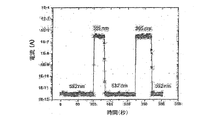
図1は、ZnOナノワイヤを電極に接続した後、波長が365nm及び532nmの光を交互に照射する時の電流の流れを示すグラフで、ZnOナノワイヤの電気抵抗が、波長365nmの光を照射時に著しく変化する特性を示している。このようなナノワイヤの特定波長に対する電気抵抗の変化は、照射量(Pumping power)によるナノワイヤの通電電流を示す図2のように、照射する光量に対しても定量的な特性を示している。図3は、光照射によるナノワイヤ貫通電流(光電流)と暗電流とを比較したグラフである。ここに示すように、ナノワイヤに加えた照射光によってナノワイヤに流れる電流が干渉要因として作用する暗電流に比べて著しく高い数値を示すため、高い信号対雑音比の確保が可能である。 FIG. 1 is a graph showing the flow of current when alternately irradiating light with a wavelength of 365 nm and 532 nm after connecting a ZnO nanowire to an electrode. The electrical resistance of the ZnO nanowire is noticeable when irradiating light with a wavelength of 365 nm. It shows changing characteristics. Such a change in electrical resistance with respect to a specific wavelength of the nanowire has a quantitative characteristic with respect to the amount of light to be irradiated as shown in FIG. 2 which shows an energization current of the nanowire depending on the irradiation power (Pumping power). FIG. 3 is a graph comparing nanowire through current (photocurrent) and dark current by light irradiation. As shown here, the current flowing through the nanowire due to the irradiation light applied to the nanowire shows a significantly higher value than the dark current acting as an interference factor, so that a high signal-to-noise ratio can be ensured.
本発明において、ナノワイヤ光センサが所望の波長帯域で光感応を起こすように制御するために、次のような特性を有するナノワイヤを使用することができる。 In the present invention, a nanowire having the following characteristics can be used to control the nanowire optical sensor so as to cause photosensitivity in a desired wavelength band.
第1に、ナノワイヤは、構成物質によって異なる感応波長を有するため、適切な構成物質を選択してナノワイヤ光センサが所望の波長帯域で光感応を起こすようにすることができる。ここで、感応波長が異なる2つ以上のナノワイヤを使用してナノワイヤ光センサの感応波長を調節することができる。このような感応波長の調節は、感応波長が異なる複数のナノワイヤサスペンションを混合液にして光センサ基板に配列させる方法で可能である。本発明の実施形態で使用されるナノワイヤ構成物質の波長帯域を以下の表1に示す。 First, since nanowires have different sensitive wavelengths depending on the constituent materials, an appropriate constituent material can be selected to cause the nanowire optical sensor to be sensitive in a desired wavelength band. Here, the sensitive wavelength of the nanowire optical sensor can be adjusted using two or more nanowires having different sensitive wavelengths. Such adjustment of the sensitive wavelength is possible by a method in which a plurality of nanowire suspensions having different sensitive wavelengths are mixed and arranged on a photosensor substrate. The wavelength bands of the nanowire constituent materials used in the embodiments of the present invention are shown in Table 1 below.

第2に、従来のナノワイヤに適切な不純物がドーピングされたナノワイヤを使用することにより、ナノワイヤ光センサが所望の波長帯域で光感応を起こすように調節することができる。不純物は、電子ドナー及び電子アクセプタの役割を果たし得る不純物で、約0.5〜5%添加する。例えば、GaNナノワイヤの場合、ドナーは、SiまたはGe、アクセプタは、Mg、Mn、CoまたはFeなどを使用することができる。SiCナノワイヤの場合、ドナーは、N、アクセプタは、BまたはAlなどを使用することができる。ZnOナノワイヤの場合、ドナーは、SiまたはAl、アクセプタは、NまたはLiなどを使用することができる。SiやGeナノワイヤの場合、ドナーは、Li、P、As、SbまたはS、アクセプタは、B、Al、Zn、In、GaまたはNiなどを使用することができる。InPまたはGaPナノワイヤの場合、ドナーは、Si、NまたはAs、アクセプタは、Mg、MnまたはZnなどを使用することができる。AlAsまたはGaAsナノワイヤの場合、ドナーは、Si、アクセプタは、Mg、MnまたはZnなどを使用することができる。InNナノワイヤの場合、ドナーは、SiまたはGe、アクセプタは、Mg、Mn、Znなどを使用することができる。CdSやCdSeナノワイヤの場合、ドナーは、SiまたはGe、アクセプタは、Mgなどを使用することができる。 Secondly, the nanowire optical sensor can be adjusted to be light sensitive in a desired wavelength band by using a nanowire in which a conventional nanowire is doped with appropriate impurities. The impurity is an impurity that can serve as an electron donor and an electron acceptor, and is added at about 0.5 to 5%. For example, in the case of a GaN nanowire, Si or Ge can be used as the donor, and Mg, Mn, Co, or Fe can be used as the acceptor. In the case of a SiC nanowire, N can be used as the donor, and B or Al can be used as the acceptor. In the case of a ZnO nanowire, Si or Al can be used as a donor, and N or Li can be used as an acceptor. In the case of Si or Ge nanowires, Li, P, As, Sb or S can be used as a donor, and B, Al, Zn, In, Ga, Ni, or the like can be used as an acceptor. In the case of InP or GaP nanowires, Si, N or As can be used as a donor, and Mg, Mn, Zn, or the like can be used as an acceptor. In the case of AlAs or GaAs nanowires, Si can be used as the donor, and Mg, Mn, Zn, or the like can be used as the acceptor. In the case of InN nanowires, Si or Ge can be used as a donor, and Mg, Mn, Zn, or the like can be used as an acceptor. In the case of CdS or CdSe nanowires, Si or Ge can be used as a donor, and Mg can be used as an acceptor.
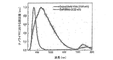
図4は、GaNナノワイヤに微量物質(Mn、4%)をドーピングする時に観察される波長帯域の変化を示す図で、ここから分かるように、微量の不純物をドーピングすることで、波長帯域の調節が可能で、不純物の種類及びドーピング量を調節することで、光センサに使用されるナノワイヤが感応する波長帯域を調節することができる。 FIG. 4 is a graph showing changes in the wavelength band observed when a GaN nanowire is doped with a trace substance (Mn, 4%). As can be seen, the wavelength band is adjusted by doping a trace amount of impurities. The wavelength band to which the nanowire used in the optical sensor is sensitive can be adjusted by adjusting the type of impurities and the doping amount.
第3に、半径方向に異種構造を有するナノワイヤを使用し、ナノワイヤ光センサが所望の波長帯域で光感応を起こすように調節することができる。半径方向に異種構造は、1つの物質を蒸着してコア部分を形成した後、その周囲に他の物質を蒸着してシース部分を形成することで得ることができる。例えば、図5は、GaN−ZnO半径方向の異種構造のナノワイヤの外観を示す図であり、図6は、異種構造のナノワイヤに現れる波長帯域の変化を示すグラフである。図5及び図6から分かるように、2種類の物質がそれぞれコアとシースを構成する異種構造のナノワイヤは、コアとシースがそれぞれ異なる波長帯域で光感応を起こし得るために、より広い領域で光反応を達成することができる。また、半径方向に異種構造でコアとシースの厚さを調節することで、量子制限効果によって光感応を起こす波長帯域を調節することができる。すなわち、各半導体が有する固有のボーアエキシトン半径(Bohr exciton radius)より小さくなるようにコアとシースの厚さを調節すると、光感応波長帯域を調節することができる。例えば、GaN−ZnO異種構造の場合、各部分、または一部分の厚さを10nm以下に調節すると、量子制限効果によってより短い波長帯で光感応を起こすことができる。 Third, a nanowire having a heterogeneous structure in the radial direction can be used and the nanowire optical sensor can be adjusted so as to be light sensitive in a desired wavelength band. A heterogeneous structure in the radial direction can be obtained by depositing one material to form a core portion and then depositing another material around it to form a sheath portion. For example, FIG. 5 is a diagram showing the appearance of nanowires with different structures in the radial direction of GaN-ZnO, and FIG. 6 is a graph showing changes in wavelength bands appearing in the nanowires with different structures. As can be seen from FIGS. 5 and 6, the nanowires of different structures in which two kinds of materials constitute the core and the sheath can cause photosensitivity in different wavelength bands, so that the light in a wider region can be obtained. A reaction can be achieved. In addition, by adjusting the thicknesses of the core and the sheath with different structures in the radial direction, the wavelength band that causes photosensitivity by the quantum limiting effect can be adjusted. That is, the photosensitive wavelength band can be adjusted by adjusting the thickness of the core and the sheath so as to be smaller than the intrinsic Bohr exciton radius of each semiconductor. For example, in the case of a GaN-ZnO heterostructure, when the thickness of each part or part is adjusted to 10 nm or less, photosensitivity can be caused in a shorter wavelength band due to the quantum limiting effect.
第4に、長手方向に異種構造を有するナノワイヤを使用し、ナノワイヤ光センサが所望の波長帯域で光感応を起こすように調節することができる。長手方向に異種構造は、異なる2種類以上の物質を交互に蒸着させることで得ることができる。このように、2種類の物質が長手方向にそれぞれ交互に構成された異種構造のナノワイヤは、各領域毎にそれぞれ異なる波長帯域で光感応を起こし得るために、より広い波長帯域で光感応を達成することができる。例えば、同一のIII-V化合物半導体で、同一の結晶構造を有するInNとGaNで長手方向の異種構造を有するナノワイヤを製造することができて、このようなナノワイヤにおいてInN部分は、500〜800nm波長帯域で光感応を起こし、GaN部分は、360nm以下の波長帯域で光感応を起こす。 Fourth, a nanowire having a heterogeneous structure in the longitudinal direction can be used, and the nanowire optical sensor can be adjusted to cause photosensitivity in a desired wavelength band. A heterogeneous structure in the longitudinal direction can be obtained by alternately depositing two or more different substances. In this way, nanowires with different structures in which two kinds of substances are alternately arranged in the longitudinal direction can cause photosensitivity in different wavelength bands in each region, and thus achieve photosensitivity in a wider wavelength band. can do. For example, a nanowire having a heterogeneous structure in the longitudinal direction of InN and GaN having the same crystal structure can be manufactured using the same III-V compound semiconductor. In the nanowire, the InN portion has a wavelength of 500 to 800 nm. Photosensitivity occurs in the band, and the GaN portion causes photosensitivity in a wavelength band of 360 nm or less.
第5に、半径方向に異種構造のナノワイヤにおいて内部を除去したチューブ状のナノワイヤを使用し、ナノワイヤ光センサが所望の波長帯域で光感応を起こすように調節することができる。この場合、チューブの厚さに応じて量子制限効果により光感応波長帯域を調節することができる。ナノワイヤを塩酸で処理するか、または高温の還元雰囲気(例えば、H2、500℃、30分)下で処理すると、高温還元雰囲気に弱いコア部分を除去することができる。すなわち、コア部分を除去して残ったチューブの厚さを調節することで、光感応波長帯域を調節することができる。例えば、チューブの厚さが材料固有のボーアエキシトン半径より小さくなるように調節すると、量子制限効果によってより短い波長帯で光感応を起こすことができる。 Fifth, it is possible to adjust the nanowire optical sensor so that it is light sensitive in a desired wavelength band by using a tubular nanowire in which the inside of the nanowire having a heterogeneous structure is removed in the radial direction. In this case, the photosensitive wavelength band can be adjusted by the quantum limiting effect according to the thickness of the tube. When the nanowire is treated with hydrochloric acid or under a high-temperature reducing atmosphere (for example, H 2 , 500 ° C., 30 minutes), the core portion weak in the high-temperature reducing atmosphere can be removed. That is, the photosensitive wavelength band can be adjusted by adjusting the thickness of the remaining tube after removing the core portion. For example, if the tube thickness is adjusted to be smaller than the intrinsic Bohr exciton radius, photosensitivity can be caused in a shorter wavelength band due to the quantum limiting effect.
第6に、固溶したナノワイヤを使用し、ナノワイヤ光センサが所望の波長帯域で光感応を起こすように調節することができる。例えば、III-V化合物のうちInNとGaNは、それぞれ0.7 eVと3.4 eVの波長帯域を有して互いに固溶したInxGa1-xN組成を作ることができる。ここで、波長帯域は、組成xにより調節できるため、xの調節によって620から360nmの広い領域で光反応を調節することができる。 Sixth, solid nanowires can be used and the nanowire photosensor can be adjusted to be sensitive in the desired wavelength band. For example, among the III-V compounds, InN and GaN have a wavelength band of 0.7 eV and 3.4 eV, respectively, and can produce In x Ga 1-x N compositions that are solid-solved with each other. Here, since the wavelength band can be adjusted by the composition x, the photoreaction can be adjusted in a wide region of 620 to 360 nm by adjusting x.
また、本発明は、ナノワイヤ光センサの製造方法を提供する。ナノワイヤ光センサの製造方法は、ナノワイヤを成長させた後に分離する段階、絶縁体基板上に2つの導電性金属薄膜電極を位置させる段階、得られたナノワイヤを電極間に分散させて5−50Vの範囲の電圧を加えてナノワイヤを2つの電極間に位置させる段階及び電子ビームの照射または熱処理により電極とナノワイヤを電気的に接続させる段階、を含む。電極とナノワイヤの接続時に電子ビームを利用する場合、1〜5秒間照射することが好ましく、熱処理を利用する場合、200〜500℃で10〜60秒加熱することが好ましい。 Moreover, this invention provides the manufacturing method of a nanowire optical sensor. The method for manufacturing a nanowire optical sensor includes a step of separating a nanowire after it has been grown, a step of positioning two conductive metal thin film electrodes on an insulator substrate, and dispersing the obtained nanowires between the electrodes to make 5-50V. Applying a range of voltages to position the nanowire between the two electrodes and electrically connecting the electrode and the nanowire by electron beam irradiation or heat treatment. When using an electron beam at the time of connection of an electrode and nanowire, it is preferable to irradiate for 1 to 5 seconds, and when using heat treatment, it is preferable to heat at 200 to 500 ° C. for 10 to 60 seconds.
電極として、Au、Ti、Pt、Pd、TiN及びこれらのうち2つ以上の合金からなる群から選択される物質を使用することが好ましく、同一または異なる物質からなる2つの電極を絶縁体の基板上に適切な距離を置いて位置させる。電極間の距離は、ナノワイヤの長さより短い2−100マイクロメートルの範囲で調節することが好ましい。ナノワイヤとして、一般的な半導体物質から、好ましくは、ZnO、SnO2、CdSe、GaN、CdS、InP、GaP、GaAs、AlAs、InN、Si、Ge及びSiCからなる群から選択された何れか1つの物質から形成され、直径が1〜100ナノメートルの範囲のものを使用することが好ましい。 Preferably, a material selected from the group consisting of Au, Ti, Pt, Pd, TiN and an alloy of two or more of these is used as the electrode, and two electrodes made of the same or different materials are used as the insulating substrate. Place it at an appropriate distance above. The distance between the electrodes is preferably adjusted in the range of 2 to 100 micrometers shorter than the length of the nanowire. The nanowire is any one selected from the group consisting of common semiconductor materials, preferably ZnO, SnO 2 , CdSe, GaN, CdS, InP, GaP, GaAs, AlAs, InN, Si, Ge and SiC. It is preferable to use a material formed from a substance and having a diameter in the range of 1 to 100 nanometers.
ナノワイヤは、所定のシリコンなどの半導体、サファイアなどのセラミック、ガラス、高分子及びプラスチック基板から選択された所定の基板に貴金属または遷移金属触媒を位置させて、300〜800℃の範囲の高温でナノワイヤ成分の所定の前駆体を供給して成長させた後、基板からナノワイヤを分離させて使用する。遷移金属触媒として、Au、Ni、CoまたはNiなどを使用することができる。ここで、ナノワイヤが成長した基板がアルコールまたはナノワイヤと反応しない場合、容易に揮発する有機溶媒に入れて数秒間超音波を加えて基板からナノワイヤを分離させて、ナノワイヤが含まれたサスペンション状態の溶液を作って使用することができる。例えば、有機溶媒としてイソプロピルアルコールなどを使用することができる。 The nanowire is a nanowire formed at a high temperature in the range of 300 to 800 ° C. by placing a noble metal or transition metal catalyst on a predetermined substrate selected from a semiconductor such as silicon, a ceramic such as sapphire, glass, a polymer, and a plastic substrate. After supplying a predetermined precursor of the component and growing it, the nanowire is separated from the substrate and used. Au, Ni, Co, Ni or the like can be used as the transition metal catalyst. Here, when the substrate on which the nanowires are grown does not react with alcohol or nanowires, it is placed in an easily volatile organic solvent and ultrasonic waves are applied for several seconds to separate the nanowires from the substrate, and the suspension solution containing nanowires Can be made and used. For example, isopropyl alcohol or the like can be used as the organic solvent.
ここで、ナノワイヤは、所望の光感応範囲を有する物質を選択して成長させて、前述のように、適切な不純物をドーピングさせるか、異なる2つの物質を使用して半径方向に異種構造または長手方向に異種構造を有するように作製するか、またはチューブ状に作製するか、または固溶したナノワイヤを作製することで、ナノワイヤ光センサが所望の波長帯域で光感応を起こすように調節することができる。 Here, the nanowire is grown by selecting and growing a material having a desired light-sensitive range, and doping the appropriate impurities as described above, or using two different materials to form a heterogeneous structure or length in the radial direction. It is possible to adjust the nanowire optical sensor to be light sensitive in a desired wavelength band by making it to have a heterogeneous structure in the direction, making it in a tube shape, or making a solid solution nanowire. it can.
本発明の一実施形態においては、ナノワイヤ溶液を絶縁体の基板上に位置する2つの電極間に少量位置させて電場をかけることによってナノワイヤを電極間に位置させることができる。本発明の他の実施形態においては、ナノワイヤ溶液をラングミュア-ブロジェット膜状に作製して圧着することによって電極間に位置させることができる。または、本発明が属する技術分野で通常に使用される他の所定の方法を用いてナノワイヤを電極間に位置させることができる。 In one embodiment of the present invention, the nanowires can be positioned between the electrodes by placing a small amount of the nanowire solution between the two electrodes positioned on the insulator substrate and applying an electric field. In another embodiment of the present invention, the nanowire solution can be positioned between the electrodes by making a Langmuir-Blodgett film and pressing it. Alternatively, the nanowires can be positioned between the electrodes using other predetermined methods commonly used in the technical field to which the present invention belongs.
次いで、数秒間の電子ビームの照射または加熱によって電極をナノワイヤと電気的に接続させる。ナノワイヤが電気的に接続されたか否かは、光学顕微鏡を使用した肉眼検査と、特定波長を照射した後に抵抗の変化を観察する電気的な検査法とを順次行って確認する。この時、光センサの2つの電極に所定電圧を加えて測定し、光照射量は、ナノワイヤの抵抗の変化によってナノワイヤに流れる電流量を測定して換算する。 Next, the electrode is electrically connected to the nanowire by irradiation or heating with an electron beam for several seconds. Whether or not the nanowires are electrically connected is confirmed by sequentially performing a visual inspection using an optical microscope and an electrical inspection method for observing a change in resistance after irradiation with a specific wavelength. At this time, measurement is performed by applying a predetermined voltage to the two electrodes of the optical sensor, and the amount of light irradiation is converted by measuring the amount of current flowing through the nanowire due to a change in the resistance of the nanowire.
また、本発明は、化学蛍光物質を含む検出ストリップとナノワイヤ光センサを含み、ナノワイヤ光センサが化学蛍光の発生する部分に密着して位置する化学蛍光測定キットを提供する(図8参照)。化学蛍光測定キットは、迅速診断キットとして使用可能である。 In addition, the present invention provides a chemical fluorescence measurement kit including a detection strip containing a chemical fluorescent substance and a nanowire optical sensor, wherein the nanowire optical sensor is positioned in close contact with a portion where chemical fluorescence is generated (see FIG. 8). The chemifluorescence measurement kit can be used as a rapid diagnostic kit.
このようなナノワイヤを使用した光センサは、図8のように迅速診断キットの化学蛍光が行われる部分に密着するように位置させる。一般に使用される蛍光物質のうちナノワイヤが感応し得る波長に適した蛍光波長を有するものを選択し、これを検出ストリップの何れか一部分以上(例えば、信号線及び確認線)にコーティングして使用する。このような蛍光の測定のために使用される蛍光物質別に励起波長と蛍光波長に使用されたナノワイヤを以下の表2に整理した。 An optical sensor using such a nanowire is positioned so as to be in close contact with the portion of the rapid diagnostic kit where chemical fluorescence is performed as shown in FIG. A fluorescent substance having a fluorescent wavelength suitable for a wavelength to which the nanowire can be sensitive is selected from among commonly used fluorescent substances, and this is coated on any part or more (for example, a signal line and a confirmation line) of the detection strip. . The nanowires used for the excitation wavelength and the fluorescence wavelength are arranged in Table 2 below for each fluorescent substance used for the measurement of fluorescence.
表2に示すように、500〜800nmの波長帯域において、InP、GaP、GaAs、AlAs、InN、Siなどのナノワイヤから与えられた波長帯域に反応し得るナノワイヤを選択、使用した。または、与えられた波長帯域に適した半径方向に異種構造のナノワイヤを選択することができる。または、与えられた波長帯域に適した長手方向に異種構造のナノワイヤを選択することができ。または、与えられた波長帯域に適したナノチューブを選択することができる。または、与えられた波長帯域に適した固溶したナノワイヤを選択することができる。このように蛍光物質が示す蛍光波長によって適切に光センサに使用されるナノワイヤを選択する。 As shown in Table 2, in the wavelength band of 500 to 800 nm, nanowires that can react to the wavelength band given from nanowires such as InP, GaP, GaAs, AlAs, InN, and Si were selected and used. Alternatively, nanowires of different structures can be selected in the radial direction suitable for a given wavelength band. Alternatively, nanowires of different structures can be selected in the longitudinal direction suitable for a given wavelength band. Alternatively, nanotubes suitable for a given wavelength band can be selected. Alternatively, a solid solution nanowire suitable for a given wavelength band can be selected. Thus, the nanowire used for an optical sensor is appropriately selected according to the fluorescence wavelength indicated by the fluorescent material.
また、本発明は、化学発光基質及び化学発光酵素を含む検出ストリップとナノワイヤ光センサを含み、ナノワイヤ光センサが化学発光の発生する部分に密着して位置する化学発光測定キットを提供する(図8参照)。化学発光測定キットは、迅速診断キットとして使用可能である。 The present invention also provides a chemiluminescence measuring kit including a detection strip including a chemiluminescent substrate and a chemiluminescent enzyme and a nanowire optical sensor, wherein the nanowire optical sensor is positioned in close contact with a portion where chemiluminescence occurs (FIG. 8). reference). The chemiluminescence measurement kit can be used as a rapid diagnostic kit.
このようなナノワイヤを使用した光センサは、図8のように迅速診断キットの化学発光が行われる部分(例えば、信号線と確認線)に密着するように位置させる。一般に使用される発光基質のうちナノワイヤが感応し得る波長に適した発光波長を有するものを選択し、これを検出ストリップの何れか一部分以上にコーティングして検出対象基質として使用し、検出基質に作用する化学発光酵素を注入して化学発光を発生させてこれを測定する。例えば、ホースラディシュ・ペルオキシダーゼ(HRP)、アルカリホスファターゼ(AP)及びルシフェラーゼの発光基質のうち、表2に提示された波長範囲で定量的な化学発光を起こすアダマンタン-ジオキセタン(Adamantane-dioxetane)、アクリジニウム(Acridinium)誘導体、ルミノール(Luminol)誘導体、ルシゲニン(Lucigenin)、ホタルルシフェリン(Firefly luciferin)、エクオリン(Aequorin)などを含む発光蛋白質(Photoprotein)、ヒドラジド(Hydrazide)及びシッフ(Schiff)塩基化合物、ルテニウムトリスビピリジル基(Ruthenium trisbipyridyl group)を含む電気化学的な発光基質及び発光性酸素チャネリング基質などをコーティングして検出対象基質として使用することができる。発光基質別に発光波長と前記波長に感応するナノワイヤを以下の表3に整理した。 An optical sensor using such a nanowire is positioned so as to be in close contact with a portion (for example, a signal line and a confirmation line) where chemiluminescence is performed in the rapid diagnostic kit as shown in FIG. Select a commonly used luminescent substrate with a wavelength suitable for the nanowire's sensitive wavelength, and coat it on any part of the detection strip and use it as the target substrate for detection. A chemiluminescent enzyme is injected to generate chemiluminescence, and this is measured. For example, among the radiant substrates of horseradish peroxidase (HRP), alkaline phosphatase (AP) and luciferase, adamantane-dioxetane, acridinium (Adamantane-dioxetane) that causes quantitative chemiluminescence in the wavelength range presented in Table 2 Photoproteins including Acridinium derivatives, Luminol derivatives, Lucigenin, Firefly luciferin, Aequorin, hydrazide and Schiff base compounds, ruthenium trisbipyridyl An electrochemical luminescent substrate containing a group (Ruthenium trisbipyridyl group) and a luminescent oxygen channeling substrate can be coated and used as a detection target substrate. The emission wavelength and the nanowires sensitive to the wavelength are arranged in Table 3 below for each luminescent substrate.
表3に示すように、430nmの波長帯では、ナノワイヤとしてドーピングされたGaNまたはドーピングされたZnOナノワイヤを使用し、これより長波長帯では、InP、GaP、GaAs、AlAs、InN、SiまたはGeナノワイヤのうち適切なものを選択して使用する。または、与えられた波長帯に適するように2つの物質を選択してコア及びシース構造を有する半径方向に異種構造のナノワイヤを使用することができる。または、与えられた波長帯に適するように2つの物質を選択して交互に蒸着させることで得られる長手方向に異種構造のナノワイヤを使用することができる。または、2つの物質を適切に固溶したナノワイヤを使用することができる。このように発光基質が示す発光波長によって光センサに使用されるナノワイヤを選択する。 As shown in Table 3, in the wavelength band of 430 nm, doped GaN or doped ZnO nanowires are used, and in the longer wavelength band, InP, GaP, GaAs, AlAs, InN, Si, or Ge nanowires are used. Select and use the appropriate one. Alternatively, nanowires with different structures in the radial direction having a core and a sheath structure can be selected by selecting two materials to suit a given wavelength band. Alternatively, it is possible to use nanowires having different structures in the longitudinal direction obtained by selecting and depositing two substances alternately so as to be suitable for a given wavelength band. Alternatively, a nanowire in which two substances are appropriately dissolved can be used. Thus, the nanowire used for the optical sensor is selected according to the emission wavelength indicated by the luminescent substrate.
ナノワイヤを利用する光センサは、迅速診断キットに内蔵し得るように小型化が容易で、使い捨て使用ができるように生産コストが低く、使用現場で別途の外部機器なしに使用が可能である。また、ナノワイヤを使用する光スイッチの場合、一般のCCD素子や光ダイオードとは異なり、感応する光波長帯域が狭くて別途の光遮断装置なしに迅速診断キット用プラスチック容器内に内蔵して使用が可能で、消費電力が小さくて迅速診断キットに内蔵可能なボタン型電池を使用して駆動が可能である。 An optical sensor using nanowires can be easily miniaturized so that it can be incorporated in a rapid diagnostic kit, has a low production cost so that it can be used disposablely, and can be used without a separate external device at the site of use. Also, in the case of optical switches using nanowires, unlike ordinary CCD devices and photodiodes, the sensitive optical wavelength band is narrow and can be used by being embedded in a plastic container for a rapid diagnostic kit without a separate light blocking device. It can be driven using a button-type battery that has low power consumption and can be built into a rapid diagnostic kit.
また、本発明は、ナノワイヤ光センサと分析対象物を含む免疫分析キットを提供する。免疫分析キットは、分析対象物が、オリゴヌクレオチド、DNA、RNA、PNA及びcDNAを含む核酸である核酸検出チップ及び分析対象物が蛋白質である蛋白質チップを含む。 The present invention also provides an immunoassay kit including a nanowire optical sensor and an analysis object. The immunoassay kit includes a nucleic acid detection chip whose analysis object is a nucleic acid including oligonucleotide, DNA, RNA, PNA and cDNA, and a protein chip whose analysis object is a protein.
まず、本発明のナノワイヤ光センサを、従来の蛍光反応を利用する核酸検出チップ及び蛋白質チップに応用することができる。核酸検出チップを使用して遺伝子を検出する場合、チップに固定された遺伝子に相補的な遺伝子が結合されたか否かを確認するために、相補的に結合する遺伝子に蛍光物質を連結してここから発生する蛍光を測定することが一般的である。実際に、蛍光の確認は、特定波長のレーザを照射して蛍光を励起してシフトされた波長の光量を測定して行われる。蛍光の測定は、一般に光源として使用されるレーザの光路と90゜の角度で行われる。ここで、光源と90゜の角度に使用された蛍光物質の蛍光波長に適した波長帯域を有するナノワイヤを使用する本発明のナノワイヤ光センサを装置することにより、発生する蛍光を測定することができる。 First, the nanowire optical sensor of the present invention can be applied to a conventional nucleic acid detection chip and protein chip using a fluorescence reaction. When a gene is detected using a nucleic acid detection chip, a fluorescent substance is linked to a complementary binding gene to confirm whether a complementary gene is bound to the gene immobilized on the chip. It is common to measure the fluorescence generated from the. Actually, the confirmation of the fluorescence is performed by irradiating a laser having a specific wavelength to excite the fluorescence and measuring the light amount of the shifted wavelength. The measurement of fluorescence is generally performed at an angle of 90 ° with the optical path of a laser used as a light source. Here, the generated fluorescence can be measured by installing the nanowire optical sensor of the present invention using a nanowire having a wavelength band suitable for the fluorescence wavelength of the fluorescent material used at an angle of 90 ° with the light source. .
また、本発明の化学発光測定が可能なナノワイヤ光センサを核酸検出チップまたは蛋白質チップに適用することができる。このために、チップに固定された遺伝子に結合する相補的な遺伝子に化学発光を誘導し得る酵素であるHRP、AP、ルシフェラーゼなどを結合させて化学発光基質を注入することにより、検出を行うことができる。一般に蛍光で検出が可能な限界は、10-12 Mであるのに比べて、化学発光で検出可能な限界は、10-19 Mで、化学発光を使用する場合、化学蛍光を使用する場合より高い感度の検出が可能である。従って、PCR方法を用いて対象遺伝子を増幅しないか、または少ない回数の増幅で微量の分析対象遺伝子を検出し得るという利点があるため、検査時間が短縮され、PCR過程で発生し得る誤増幅による検出のミスを減らし得るという利点がある。また、レーザなどの別途の光源を必要としないという利点があって、マイクロスケールの小型化が容易で、集積によるアレイ化が可能で核酸検出チップへの応用に有利である。 Moreover, the nanowire optical sensor capable of chemiluminescence measurement of the present invention can be applied to a nucleic acid detection chip or a protein chip. For this purpose, detection is performed by injecting a chemiluminescent substrate by binding HRP, AP, luciferase, etc., which are enzymes capable of inducing chemiluminescence, to a complementary gene that binds to the gene fixed on the chip. Can do. In general, the limit that can be detected by fluorescence is 10 −12 M, whereas the limit that can be detected by chemiluminescence is 10 −19 M. When chemiluminescence is used, it is more than when chemiluminescence is used. High sensitivity detection is possible. Therefore, there is an advantage in that the target gene is not amplified using the PCR method, or a small amount of the target gene can be detected with a small number of amplifications, so that the test time is shortened, resulting in erroneous amplification that may occur in the PCR process. There is an advantage that detection errors can be reduced. In addition, there is an advantage that a separate light source such as a laser is not required, micro-scale miniaturization is easy, and an array by integration is possible, which is advantageous for application to a nucleic acid detection chip.
また、本発明は、蛋白質チップにおいて、蛋白質が固定されていて試料内の蛋白質または化学物質からなる結合物質が固定された蛋白質に結合するか、または生成物を作るが、ここで、結合物質または生成物に蛍光物質を標識し、蛍光物質の蛍光波長に適したナノワイヤを含む本発明のナノワイヤ光センサを使用して発生する蛍光を測定することで、酵素と基質との反応、受容体(合成または生物受容体)と結合物の反応、抗原抗体反応などの蛋白質間の結合、蛋白質と遺伝子(DNAまたはRNA)との結合、遺伝子(DNAまたはRNA)間の結合を検出し得る蛋白質チップを提供することができる。 The present invention also relates to a protein chip in which a protein is immobilized and a binding substance consisting of a protein or chemical substance in the sample binds to the immobilized protein or creates a product. By labeling the product with a fluorescent substance and measuring the fluorescence generated using the nanowire optical sensor of the present invention including a nanowire suitable for the fluorescence wavelength of the fluorescent substance, the reaction between the enzyme and the substrate, the receptor (synthesis) Alternatively, a protein chip capable of detecting the binding between proteins such as biological receptors) and binding substances, antigen-antibody reactions, binding between proteins and genes (DNA or RNA), and binding between genes (DNA or RNA) is provided. can do.
また、本発明は、蛋白質チップにおいて、結合物質または生成物に発光酵素を結合させて発光物質を注入し、発光物質の発光波長に適したナノワイヤを含む本発明のナノワイヤ光センサを使用することで、化学発光を測定する蛋白質チップを提供することができる。蛋白質チップの場合にも核酸検出チップの場合のようにアレイに集積されても本発明のナノワイヤ光センサの適用が可能である。すなわち、酵素蛋白質の反応、受容体(合成または生物受容体)と結合物との反応、抗原−抗体反応など蛋白質間の結合、蛋白質と遺伝子(DNAまたはRNA)との結合反応など、蛍光の測定により反応するか否か及び反応量を測定する全ての検査に使用が可能である。 The present invention also provides a protein chip, wherein a luminescent enzyme is bound to a binding substance or product, a luminescent substance is injected, and the nanowire optical sensor of the present invention including a nanowire suitable for the emission wavelength of the luminescent substance is used. A protein chip for measuring chemiluminescence can be provided. The nanowire optical sensor of the present invention can be applied even if it is integrated in an array as in the case of a protein chip or a nucleic acid detection chip. That is, fluorescence measurements such as enzyme protein reactions, reactions between receptors (synthetic or biological receptors) and conjugates, binding between proteins such as antigen-antibody reactions, and binding reactions between proteins and genes (DNA or RNA). It can be used for all tests for measuring whether or not to react and the amount of reaction.
このような核酸検出チップ及び蛋白質チップを含む免疫分析キットにおいて、本発明のナノワイヤ光センサを使用してマイクロアレイ型または単一検査用蛋白質チップとして実現可能である。マイクロアレイ型の場合、複数のナノワイヤ光センサがマルチプレクサにより接続されてそれぞれの光センサの信号が順次処理されるように構成されるか、またはアナログスイッチングによりそれぞれの光センサの信号が同時に処理されるように構成することができる。 An immunoassay kit including such a nucleic acid detection chip and a protein chip can be realized as a microarray type or a single test protein chip using the nanowire optical sensor of the present invention. In the case of the microarray type, a plurality of nanowire optical sensors are connected by a multiplexer so that the signals of the respective optical sensors are sequentially processed, or the signals of the respective optical sensors are processed simultaneously by analog switching. Can be configured.
前述した蛍光及び発光の測定は、蛍光及び発光が起こる部位に近接するようにナノワイヤ光センサを固定して行われる。このような固定方法は、従来製作されていた迅速診断キット、蛋白質チップ、核酸検出チップに大きな変形をしなくても使用が可能である。 The measurement of fluorescence and luminescence described above is performed with the nanowire optical sensor fixed so as to be close to the site where fluorescence and luminescence occur. Such an immobilization method can be used without any major modification to the conventionally produced rapid diagnostic kit, protein chip, and nucleic acid detection chip.
また、信号を起こす光量の損失を減らして迅速に測定するためには、ナノワイヤ上で蛍光及び発光が起こるようにする方法が使用可能である。すなわち、前述したように、固体上に固定される反応物質をナノワイヤ上に直接固定することが実現可能である。このようなナノワイヤ上に反応物質を固定する方法は、ナノワイヤと物質間に化学連結物質(リンカー)をナノワイヤにコーティングし、連結物質に反応物質を固定する段階からなる。ナノワイヤのコーティングに使用される化学連結物質は、発生した蛍光または発光がナノワイヤに到達することを妨げないように該当波長の光を吸収しない物質を選択し、リガンド物質の結合を空間的に妨げないように薄くて均一な単一膜のようにコーティングされるべきである。金属酸化物からなるナノワイヤの場合、純粋炭素鎖あるいは、エステルのような化学官能基が鎖構造の中間に含まれた炭素鎖の末端にアミン基、カルボキシル基、エポキシ基、スルホン酸基などが結合されたチオールまたは有機シラン誘導体を処理して化学連結物質膜をナノワイヤ上に形成させることができる。有機シラン誘導体は、無水トリエトキシまたはトリメトキシ有機シラン誘導体であり得る。 In order to reduce the loss of the amount of light that causes a signal and perform measurement quickly, a method of causing fluorescence and light emission on the nanowire can be used. That is, as described above, it is possible to directly immobilize the reactant immobilized on the solid on the nanowire. Such a method of immobilizing a reactant on a nanowire includes a step of coating a nanowire with a chemical linking substance (linker) between the nanowire and the substance, and immobilizing the reactant on the linking substance. The chemical linking material used to coat the nanowire is selected so that it does not absorb the light of the corresponding wavelength so that the generated fluorescence or light emission does not prevent the nanowire from reaching the nanowire. It should be coated as a thin and uniform single film. In the case of nanowires made of metal oxides, amine groups, carboxyl groups, epoxy groups, sulfonic acid groups, etc. are bonded to the ends of pure carbon chains or carbon chains containing chemical functional groups such as esters in the middle of the chain structure. The thiol or organosilane derivative can be treated to form a chemical linking material film on the nanowire. The organosilane derivative can be an anhydrous triethoxy or trimethoxyorganosilane derivative.
また、金属酸化物、純金属、無機物などからなるナノワイヤの場合、CVD(化学蒸着法)などの過程により金属膜をコーティングした後、多様な長さの炭素鎖の末端にアミン基、カルボキシル基、エポキシ基、スルホン酸基などが結合されたチオール誘導体を処理してナノワイヤ上に化学連結物質膜を形成させることができる。 In the case of nanowires made of metal oxides, pure metals, inorganic substances, etc., after coating the metal film by a process such as CVD (chemical vapor deposition), amine groups, carboxyl groups, A thiol derivative to which an epoxy group, a sulfonic acid group, or the like is bonded can be processed to form a chemical linking material film on the nanowire.
その後、反応物質の結合は、化学連結物質の端部がカルボキシル基である場合、N−(3−ジメチルアミノプロピル)−N−エチルカルボジイミド(EDAC)及びN−ヒドロキシスクシンイミド(NHS)などを使用し、アミン基である場合には、グルタルアルデヒドなどを使用し、エポキシ基とスルホン酸基である場合には、反応物質を一定時間インキュベーションして結合を誘導する。 Thereafter, when the end of the chemical linking substance is a carboxyl group, N- (3-dimethylaminopropyl) -N-ethylcarbodiimide (EDAC) and N-hydroxysuccinimide (NHS) are used for the bonding of the reactants. In the case of an amine group, glutaraldehyde or the like is used, and in the case of an epoxy group and a sulfonic acid group, the reaction substance is incubated for a certain time to induce binding.
以上のようなナノワイヤ上に直接反応物質を結合させる方法によってナノワイヤが固定された平面に比べて、ナノワイヤの成長密度によって反応物質の結合に使用される反応面積が増加するので、使用される抗原と抗体との結合反応、酵素による反応、DNAやRNAなどを使用した結合反応などに現れるセンサ信号を大きく増幅させることができる。 Compared to the plane where the nanowire is fixed by the method of directly bonding the reactant on the nanowire as described above, the reaction area used for binding of the reactant is increased by the growth density of the nanowire. Sensor signals appearing in binding reactions with antibodies, reactions with enzymes, binding reactions using DNA, RNA, etc. can be greatly amplified.
以下、本発明によるナノワイヤ光センサを製造し、このセンサを化学発光物質と組み合わせて迅速診断キットを製造して性能を試験した実施例について記述する。下記の実施例によって本発明がより具体的に説明されるが、このような実施例は、単に本発明の例示であり、本発明がこれら実施例によって限定されるものではない。 In the following, examples are described in which a nanowire optical sensor according to the present invention is manufactured, and this sensor is combined with a chemiluminescent material to manufacture a rapid diagnostic kit to test its performance. The present invention will be described more specifically by the following examples. However, such examples are merely illustrative of the present invention, and the present invention is not limited to these examples.
[実施例]
実施例1
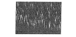
シリコン基板の一面にスパッタリング蒸着法でAuを2nmの厚さで蒸着し、この基板にCVDによって500℃でInCl3とNH3を供給することで、InNナノワイヤを成長させた。図9は、基板に成長したInNナノワイヤを示す図である。この基板をイソプロピルアルコールに入れて10秒間超音波を加えて基板からナノワイヤを分離した。溶液をTi/Au電極が位置する基板に分散して電極間に20Vの電位差を加えて電極間にナノワイヤを整列して位置させた。次いで、加熱(500℃、30秒)または電子ビームを照射して電極をナノワイヤと接続させてナノワイヤセンサを製作した。電気的な接続を確認した後、図7に示すように、作製されたナノワイヤセンサを化学発光が起こる信号線と確認線に密着するように位置させた。この時、検出対象基質は、ルミノール誘導体を使用した。この時、化学発光が起こった状態で現れる電流の変化を図10に示す。このような電流の変化で対象物質に対する検出の結果を確認することができる。
[Example]
Example 1
InN nanowires were grown by depositing Au with a thickness of 2 nm on one surface of a silicon substrate by sputtering and supplying InCl 3 and NH 3 to the substrate at 500 ° C. by CVD. FIG. 9 is a diagram showing InN nanowires grown on a substrate. The substrate was placed in isopropyl alcohol and ultrasonic waves were applied for 10 seconds to separate the nanowires from the substrate. The solution was dispersed on the substrate on which the Ti / Au electrode was positioned, and a potential difference of 20 V was applied between the electrodes to align the nanowires between the electrodes. Next, heating (500 ° C., 30 seconds) or irradiation with an electron beam was performed to connect the electrode to the nanowire, thereby producing a nanowire sensor. After confirming the electrical connection, as shown in FIG. 7, the fabricated nanowire sensor was positioned so as to be in close contact with the signal line and the confirmation line where chemiluminescence occurs. At this time, a luminol derivative was used as the detection target substrate. FIG. 10 shows the change in current that appears when chemiluminescence occurs. The detection result for the target substance can be confirmed by such a change in current.
実施例2
サファイア基板の一面にスパッタリング蒸着法でNiを2nmの厚さで蒸着し、この基板にCVDによって700℃でTMG(trimethylgallium)、NH3及び少量のCp2Mgを供給してMgがドーピングされたGaNナノワイヤを成長させた。合成したナノワイヤを用いて実施例1と同様の方法で診断キットを構成した。ここで、検出対象基質は、アクリジニウム化合物を使用し、ナノワイヤに現れる電流の変化で対象物質に対する検出の結果を確認した。
Example 2
Ni is deposited to a thickness of 2 nm on one surface of the sapphire substrate by sputtering deposition, and TMG (trimethylgallium), NH 3 and a small amount of Cp2Mg are supplied to the substrate at 700 ° C. by CVD to form Mg-doped GaN nanowire Grown up. A diagnostic kit was constructed in the same manner as in Example 1 using the synthesized nanowires. Here, an acridinium compound was used as the detection target substrate, and the detection result for the target substance was confirmed by a change in current appearing in the nanowire.
実施例3
サファイア基板の一面にスパッタリング蒸着法でNiを2nmの厚さで蒸着し、この基板にIn金属を位置させて、NH3を供給しながらInNナノワイヤを成長させた。合成したナノワイヤを用いて実施例1と同様の方法で診断キットを構成した。この時、検出対象基質は、発光蛋白質を使用し、ナノワイヤに現れる電流の変化で対象物質に対する検出の結果を確認した。
Example 3
Ni was deposited to a thickness of 2 nm on one surface of the sapphire substrate by sputtering deposition, In metal was positioned on this substrate, and InN nanowires were grown while supplying NH 3 . A diagnostic kit was constructed in the same manner as in Example 1 using the synthesized nanowires. At this time, a photoprotein was used as a detection target substrate, and the detection result for the target substance was confirmed by a change in current appearing in the nanowire.
実施例4
サファイア基板の一面にスパッタリング蒸着法でNiを2nmの厚さで蒸着し、この基板にCVDによって700℃でTMG(trimethylgallium)、NH3を供給してGaNナノワイヤを成長させた。次いで、DEZ(dethyl zinc)とO2を継続して供給してコアはGaN、シースはZnOから構成された半径方向に異種構造を有するナノワイヤを合成した。合成したナノワイヤを用いて実施例1と同様の方法で診断キットを構成した。ここで、検出対象基質は、アクリジニウム化合物を使用し、ナノワイヤに現れる電流の変化で対象物質に対する検出の結果を確認した。
Example 4
Ni was deposited to a thickness of 2 nm on one surface of the sapphire substrate by sputtering deposition, and TMG (trimethylgallium) and NH 3 were supplied to the substrate at 700 ° C. by CVD to grow GaN nanowires. Subsequently, DEZ (dethyl zinc) and O 2 were continuously supplied to synthesize a nanowire having a heterogeneous structure in the radial direction in which the core was made of GaN and the sheath was made of ZnO. A diagnostic kit was constructed in the same manner as in Example 1 using the synthesized nanowires. Here, an acridinium compound was used as the detection target substrate, and the detection result for the target substance was confirmed by a change in current appearing in the nanowire.
実施例5
サファイア基板の一面にスパッタリング蒸着法でAuを2nmの厚さで蒸着し、この基板にCVDによって700℃でDEZ(dethyl zinc)とO2を供給してZnOナノワイヤを成長させた。次いで、TMG(trimethylgallium)、NH3を継続して供給してGaNを表面に蒸着させた。次いで、ナノワイヤをHCl溶液で12時間処理してZnOコアを除去してGaNナノチューブを合成した。合成したナノチューブを用いて実施例1と同様の方法でキットを構成した。この時、検出対象基質は、アクリジニウム化合物を使用し、ナノワイヤに現れる電流の変化で対象物質に対する検出の結果を確認した。
Example 5
Au was deposited to a thickness of 2 nm on one surface of the sapphire substrate by sputtering vapor deposition, and DEZ (dethyl zinc) and O 2 were supplied to the substrate at 700 ° C. by CVD to grow ZnO nanowires. Next, TMG (trimethylgallium) and NH 3 were continuously supplied to deposit GaN on the surface. Next, the nanowires were treated with HCl solution for 12 hours to remove the ZnO core and synthesize GaN nanotubes. A kit was constructed in the same manner as in Example 1 using the synthesized nanotubes. At this time, an acridinium compound was used as the detection target substrate, and the detection result for the target substance was confirmed by a change in current appearing in the nanowire.
実施例6
サファイア基板の一面にスパッタリング蒸着法でNiを2nmの厚さで蒸着し、この基板から2cm離隔した部分にGaとIn金属を3 : 1の質量比で混ぜて位置させて、NH3を供給しながらGa1-xInxNナノワイヤを成長させた。合成したナノワイヤを用いて実施例1と同様の方法で診断キットを構成した。この時、検出対象基質は、発光蛋白質を使用し、ナノワイヤに現れる電流の変化で対象物質に対する検出の結果を確認した。
Example 6
Ni is deposited to a thickness of 2 nm on one surface of the sapphire substrate by sputtering deposition, and Ga and In metal are mixed and positioned at a mass ratio of 3: 1 in a
実施例7
癌標識物質であるCA 125(NatuTec GmbH、Germany)をマイクロプレートに固定した後、HRPが結合されたCA 125抗体(NatuTec GmbH、Germany)を濃度を変えて結合した。次いで、ルミノールが入った発光基質溶液を加えた後、実施例1で得られたInNナノワイヤ光センサを利用して化学発光量を測定した。実験の結果、InNナノワイヤ光センサは、結合されたHRPと抗体の濃度によって定量的な反応を示した。測定結果の確認のために従来の発光及び蛍光測定装置(LS45、Perkin-Elmer)を使用して化学発光を同時に測定した。実験の結果、化学発光波長に適したナノワイヤで製造した光センサが化学発光の定量的な測定に適していることが明らかになった。
Example 7
After fixing CA 125 (NatuTec GmbH, Germany), which is a cancer labeling substance, on a microplate, CA 125 antibody (NatuTec GmbH, Germany) to which HRP was bound was bound at different concentrations. Next, after adding a luminescent substrate solution containing luminol, the amount of chemiluminescence was measured using the InN nanowire optical sensor obtained in Example 1. As a result of the experiment, the InN nanowire optical sensor showed a quantitative reaction depending on the concentration of bound HRP and antibody. In order to confirm the measurement results, chemiluminescence was simultaneously measured using a conventional luminescence and fluorescence measurement device (LS45, Perkin-Elmer). As a result of experiments, it has been clarified that an optical sensor manufactured with nanowires suitable for chemiluminescence wavelength is suitable for quantitative measurement of chemiluminescence.
実施例8
B型肝炎抗原が結合されたガラス板にフルオレセインが結合されたB型肝炎抗体を濃度を変えて結合させた。フルオレセインの励起波長である495nmのレーザを照射し、同時にInNナノワイヤ光センサでレーザと約90゜の位置で発生する蛍光を測定した。測定結果の確認のために従来の発光及び蛍光測定装置(LS45、Perkin-Elmer)を使用して蛍光を測定した。実験の結果、GaPナノワイヤ光センサは、結合されたフルオレセイン量による定量信号を示した。この実験の結果は、蛍光波長に適したナノワイヤで製造した光センサが定量的に蛍光を測定可能であることを示している。
Example 8
Hepatitis B antibody bound with fluorescein was bound to a glass plate bound with hepatitis B antigen at different concentrations. A 495 nm laser, which is the excitation wavelength of fluorescein, was irradiated, and at the same time, the fluorescence generated at a position of about 90 ° with the laser was measured with an InN nanowire optical sensor. For confirmation of the measurement results, fluorescence was measured using a conventional luminescence and fluorescence measurement device (LS45, Perkin-Elmer). As a result of the experiment, the GaP nanowire optical sensor showed a quantitative signal due to the amount of bound fluorescein. The results of this experiment show that the optical sensor manufactured with nanowires suitable for the fluorescence wavelength can measure fluorescence quantitatively.
Claims (28)
前記ナノワイヤが、中心部分が除去されたチューブ状であり、チューブの厚さを調整することで、光感応波長帯域が所望の範囲に調節される
ことを特徴とするナノワイヤ光センサ。 An insulating substrate, two conductive metal thin film electrodes, and a semiconductor nanowire connected to the two electrodes and formed from a semiconductor material, the semiconductor nanowire having a diameter of 1 to 100 nanometers and a length of the two electrodes It is made of a material whose electrical resistance is lower by photoexcitation at a specific wavelength.
Wherein the nanowires, tubular der the central portion has been removed is, nanowire light sensor, characterized in that in Rukoto to adjust the thickness of the tube, the light-sensitive wavelength band is adjusted to the desired range.
前記ナノワイヤを、中心部分が除去されたチューブ状に形成し、チューブの厚さを調整することで、光感応波長帯域を所望の範囲に調節する段階と、
絶縁体基板上に2つの導電性金属薄膜電極を間隔が前記ナノワイヤの長さより短くなるように配置する段階と、
前記得られたナノワイヤを前記2つの電極間に分散させそして電圧を加えて、前記ナノワイヤを2つの電極の間に2つの電極を接続するように配置する段階と、
電子ビームの照射または加熱によって前記電極とナノワイヤとを電気的に接続する段階と、を含むことを特徴とするナノワイヤ光センサの製造方法。 Separating nanowires having a diameter of 1 to 100 nanometers on a substrate after separating them,
The nanowire is formed in a tube shape with a central portion removed , and the thickness of the tube is adjusted to adjust the photosensitive wavelength band to a desired range; and
Disposing two conductive metal thin film electrodes on an insulator substrate such that the distance is shorter than the length of the nanowire;
Dispersing the resulting nanowire between the two electrodes and applying a voltage to place the nanowire between the two electrodes to connect the two electrodes;
And a step of electrically connecting the electrode and the nanowire by irradiation or heating with an electron beam.
蛍光物質を含む検出ストリップと、を含むことを特徴とする化学蛍光測定キット。 A nanowire optical sensor according to claim 1;
A chemifluorescence measurement kit comprising a detection strip containing a fluorescent substance.
発光酵素及び発光基質を含む検出ストリップと、を含むことを特徴とする化学発光測定キット。 A nanowire optical sensor according to claim 1;
A chemiluminescence measuring kit comprising a detection strip containing a luminescent enzyme and a luminescent substrate.
請求項11〜13の何れか一項による化学蛍光測定キットまたは請求項14〜17の何れか一項による化学発光測定キットと、を含むことを特徴とする免疫分析キット。 The analyte and
An immunoassay kit comprising the chemiluminescence measurement kit according to any one of claims 11 to 13 or the chemiluminescence measurement kit according to any one of claims 14 to 17.
Applications Claiming Priority (2)
| Application Number | Priority Date | Filing Date | Title |
|---|---|---|---|
| KR10-2004-0015629 | 2004-03-08 | ||
| KR1020040015629A KR100584188B1 (en) | 2004-03-08 | 2004-03-08 | Nanowire light sensor and kit with the same |
Related Parent Applications (1)
| Application Number | Title | Priority Date | Filing Date |
|---|---|---|---|
| JP2007502710A Division JP4660536B2 (en) | 2004-03-08 | 2005-03-08 | Nanowire optical sensor and kit including the same |
Publications (2)
| Publication Number | Publication Date |
|---|---|
| JP2010169689A JP2010169689A (en) | 2010-08-05 |
| JP5178751B2 true JP5178751B2 (en) | 2013-04-10 |
Family
ID=34918723
Family Applications (2)
| Application Number | Title | Priority Date | Filing Date |
|---|---|---|---|
| JP2007502710A Expired - Fee Related JP4660536B2 (en) | 2004-03-08 | 2005-03-08 | Nanowire optical sensor and kit including the same |
| JP2010019556A Expired - Fee Related JP5178751B2 (en) | 2004-03-08 | 2010-01-29 | Nanowire optical sensor and kit including the same |
Family Applications Before (1)
| Application Number | Title | Priority Date | Filing Date |
|---|---|---|---|
| JP2007502710A Expired - Fee Related JP4660536B2 (en) | 2004-03-08 | 2005-03-08 | Nanowire optical sensor and kit including the same |
Country Status (5)
| Country | Link |
|---|---|
| US (1) | US20070131924A1 (en) |
| EP (2) | EP1723408A4 (en) |
| JP (2) | JP4660536B2 (en) |
| KR (1) | KR100584188B1 (en) |
| WO (1) | WO2005085809A1 (en) |
Families Citing this family (23)
| Publication number | Priority date | Publication date | Assignee | Title |
|---|---|---|---|---|
| WO2007059779A2 (en) * | 2005-11-28 | 2007-05-31 | Dako Denmark A/S | Cyanine dyes and methods for detecting a target using said dyes |
| KR100704007B1 (en) | 2006-01-17 | 2007-04-04 | 한국과학기술연구원 | Lateral flow immunoassay kit based on chemiluminescence and chemifluorescence reaction and using method thereof |
| KR100923165B1 (en) | 2006-12-04 | 2009-10-23 | 한국전자통신연구원 | Suspended nanowire sensor and method for fabricating the same |
| US7786440B2 (en) * | 2007-09-13 | 2010-08-31 | Honeywell International Inc. | Nanowire multispectral imaging array |
| KR100948595B1 (en) * | 2007-11-29 | 2010-03-23 | 한국전자통신연구원 | Fabrication method of surface-modified nanowire sensor |
| JP5360739B2 (en) * | 2008-03-05 | 2013-12-04 | 独立行政法人物質・材料研究機構 | Electronic device and manufacturing method thereof |
| KR20090109980A (en) * | 2008-04-17 | 2009-10-21 | 한국과학기술연구원 | Visible-range semiconductor nanowire-based photosensor and method for manufacturing the same |
| KR100976865B1 (en) * | 2008-04-28 | 2010-08-23 | 한국기계연구원 | Wavelength detection appratus and fabricating method thereof |
| WO2010047844A2 (en) * | 2008-10-20 | 2010-04-29 | Hewlett-Packard Development Company, L. P. | Nanowire bolometer photodetector |
| WO2011034590A1 (en) * | 2009-09-18 | 2011-03-24 | Caliper Life Sciences | Compositions and methods for in vivo evaluation of bioluminescence |
| KR101135137B1 (en) * | 2010-05-03 | 2012-04-19 | 한국기계연구원 | Detection appratus for light ray |
| KR101071110B1 (en) | 2010-07-20 | 2011-10-10 | 한국과학기술원 | Nano-structured photodetector with photo-induced charge transfer elements |
| CN103575896B (en) * | 2012-07-19 | 2015-09-23 | 江苏省肿瘤医院 | Highly sensitive disposable multicomponent chemical luminescence imaging immunosensor |
| CN103937488B (en) * | 2014-03-25 | 2016-03-09 | 中国科学院理化技术研究所 | Based on the alkaline phosphatase fluorescence chemical sensor of silicon nanowires and method for making and application |
| CN105633190B (en) * | 2014-10-31 | 2017-02-22 | 中国科学院物理研究所 | Ultraviolet detector based on graphene wrapping SiC nanowires |
| CN104952976A (en) * | 2015-05-13 | 2015-09-30 | 宁波工程学院 | Production method of single-crystal silicon carbide nanowire high-sensitivity purple-light photoelectric detector |
| CN107785443A (en) * | 2016-08-26 | 2018-03-09 | 中国科学院金属研究所 | Transparent flexible non-polar GaN nano wire ultraviolet detector and preparation method thereof |
| CN107159883B (en) * | 2017-05-01 | 2019-03-29 | 福建医科大学 | Chitosan-nano platinum particle simulates oxidizing ferment |
| KR102003122B1 (en) * | 2017-08-31 | 2019-07-24 | 건국대학교 산학협력단 | A method for fixing a bio-material to a metal nanotube and a biosensor including the same |
| CN108152485B (en) * | 2017-12-12 | 2019-11-15 | 江南大学 | A kind of immunoassay method reacting triggering CdS photoelectric current based on alkaline phosphate ester enzymatic |
| KR102224541B1 (en) * | 2019-03-29 | 2021-03-05 | 연세대학교 산학협력단 | Bio-electrode, chronoamperometry device, immunoassay device and method using the same |
| EP4127822A1 (en) * | 2020-04-03 | 2023-02-08 | Magic Leap, Inc. | Wearable display systems with nanowire led micro-displays |
| CN113599369B (en) * | 2021-09-02 | 2022-12-23 | 苏州大学 | Antioxidant stress nano reagent and preparation method and application thereof |
Family Cites Families (12)
| Publication number | Priority date | Publication date | Assignee | Title |
|---|---|---|---|---|
| IL135076A0 (en) * | 2000-03-15 | 2001-05-20 | Zilber Gil | An immunoassay diagnostic probe and a method for use thereof |
| AU2002229046B2 (en) * | 2000-12-11 | 2006-05-18 | President And Fellows Of Harvard College | Nanosensors |
| TW554388B (en) * | 2001-03-30 | 2003-09-21 | Univ California | Methods of fabricating nanostructures and nanowires and devices fabricated therefrom |
| CA2447728A1 (en) * | 2001-05-18 | 2003-01-16 | President And Fellows Of Harvard College | Nanoscale wires and related devices |
| US20030035755A1 (en) * | 2001-08-16 | 2003-02-20 | Shu-Hui Chen | Organic electroluminescence (OEL)-based biochips |
| KR20030040830A (en) * | 2001-11-16 | 2003-05-23 | 박철홍 | Portable scanning device for detecting various explosives |
| US6882767B2 (en) * | 2001-12-27 | 2005-04-19 | The Regents Of The University Of California | Nanowire optoelectric switching device and method |
| US6894359B2 (en) * | 2002-09-04 | 2005-05-17 | Nanomix, Inc. | Sensitivity control for nanotube sensors |
| US7112816B2 (en) * | 2002-04-12 | 2006-09-26 | University Of South Flordia | Carbon nanotube sensor and method of producing the same |
| GB0215150D0 (en) * | 2002-07-01 | 2002-08-07 | Univ Hull | Photoelectric cell |
| US7335908B2 (en) * | 2002-07-08 | 2008-02-26 | Qunano Ab | Nanostructures and methods for manufacturing the same |
| US20040218224A1 (en) * | 2003-04-29 | 2004-11-04 | Cariffe Alan Eddy | Facsimile transmission with instruction sub-code |
-
2004
- 2004-03-08 KR KR1020040015629A patent/KR100584188B1/en active IP Right Grant
-
2005
- 2005-03-08 WO PCT/KR2005/000646 patent/WO2005085809A1/en active Application Filing
- 2005-03-08 JP JP2007502710A patent/JP4660536B2/en not_active Expired - Fee Related
- 2005-03-08 EP EP05726939A patent/EP1723408A4/en not_active Ceased
- 2005-03-08 US US10/592,239 patent/US20070131924A1/en not_active Abandoned
- 2005-03-08 EP EP13183326.1A patent/EP2672257B1/en active Active
-
2010
- 2010-01-29 JP JP2010019556A patent/JP5178751B2/en not_active Expired - Fee Related
Also Published As
| Publication number | Publication date |
|---|---|
| EP1723408A4 (en) | 2012-08-08 |
| KR100584188B1 (en) | 2006-05-29 |
| EP2672257B1 (en) | 2019-05-08 |
| US20070131924A1 (en) | 2007-06-14 |
| JP2010169689A (en) | 2010-08-05 |
| JP2007528003A (en) | 2007-10-04 |
| EP2672257A1 (en) | 2013-12-11 |
| EP1723408A1 (en) | 2006-11-22 |
| WO2005085809A1 (en) | 2005-09-15 |
| KR20050090285A (en) | 2005-09-13 |
| JP4660536B2 (en) | 2011-03-30 |
Similar Documents
| Publication | Publication Date | Title |
|---|---|---|
| JP5178751B2 (en) | Nanowire optical sensor and kit including the same | |
| Babamiri et al. | Highly sensitive bioaffinity electrochemiluminescence sensors: Recent advances and future directions | |
| Pei et al. | Sandwich-type immunosensors and immunoassays exploiting nanostructure labels: A review | |
| Zhang et al. | Multiplexed sandwich immunoassays using flow-injection electrochemiluminescence with designed substrate spatial-resolved technique for detection of tumor markers | |
| Wang et al. | Dual amplification strategy for the fabrication of highly sensitive interleukin-6 amperometric immunosensor based on poly-dopamine | |
| Forster et al. | Electrogenerated chemiluminescence | |
| Leonardi et al. | Biosensing platforms based on silicon nanostructures: A critical review | |
| US20070196239A1 (en) | Optical nanowire biosensor based on energy transfer | |
| Irrera et al. | New generation of ultrasensitive label-free optical Si nanowire-based biosensors | |
| Prabhulkar et al. | Amperometric micro-immunosensor for the detection of tumor biomarker | |
| Ma et al. | A label-free electrochemiluminescence immunosensor based on EuPO4 nanowire for the ultrasensitive detection of Prostate specific antigen | |
| Yuan et al. | Electrochemical strategies for the detection of cTnI | |
| He et al. | Dichroic mirror-assisted electrochemiluminescent assay for simultaneously detecting wild-type and mutant p53 with photomultiplier tubes | |
| WO2004011672A1 (en) | Porous nanostructured film sensor | |
| Liu et al. | CdSe quantum dots as labels for sensitive immunoassay of cancer biomarker proteins by electrogenerated chemiluminescence | |
| Liu et al. | Electrochemiluminescent biosensor with DNA link for selective detection of human IgG based on steric hindrance | |
| Fu et al. | Coreactant-free and direct electrochemiluminescence from dual-stabilizer-capped InP/ZnS nanocrystals: a new route involving n-type luminophore | |
| Wang et al. | A novel strategy for improving amperometric biosensor sensitivity using dual-signal synergistic effect for ultrasensitive detection of matrix metalloproteinase-2 | |
| Chen et al. | Sensitive electrochemical immunoassay of metallothionein-3 based on K 3 [Fe (CN) 6] as a redox-active signal and c-dots/nafion film for antibody immobilization | |
| KR20090060635A (en) | Bio sensor and method for fabricating the same | |
| Liu et al. | Recent advances in nanotechnology-enhanced biosensors for α-fetoprotein detection | |
| Prajesh et al. | Polysilicon field effect transistor biosensor for the detection of cardiac Troponin-I (cTnI) | |
| US20200025753A1 (en) | Electrochemical immunosensors | |
| US20120141327A1 (en) | Label-free biosensor | |
| Rodrigues et al. | On the detection of cTnI-a comparison of surface-plasmon optical-electrochemical-, and electronic sensing concepts |
Legal Events
| Date | Code | Title | Description |
|---|---|---|---|
| A131 | Notification of reasons for refusal |
Free format text: JAPANESE INTERMEDIATE CODE: A131 Effective date: 20120313 |
|
| A521 | Request for written amendment filed |
Free format text: JAPANESE INTERMEDIATE CODE: A523 Effective date: 20120607 |
|
| TRDD | Decision of grant or rejection written | ||
| A01 | Written decision to grant a patent or to grant a registration (utility model) |
Free format text: JAPANESE INTERMEDIATE CODE: A01 Effective date: 20121225 |
|
| A61 | First payment of annual fees (during grant procedure) |
Free format text: JAPANESE INTERMEDIATE CODE: A61 Effective date: 20130108 |
|
| R150 | Certificate of patent or registration of utility model |
Ref document number: 5178751 Country of ref document: JP Free format text: JAPANESE INTERMEDIATE CODE: R150 |
|
| R250 | Receipt of annual fees |
Free format text: JAPANESE INTERMEDIATE CODE: R250 |
|
| R250 | Receipt of annual fees |
Free format text: JAPANESE INTERMEDIATE CODE: R250 |
|
| R250 | Receipt of annual fees |
Free format text: JAPANESE INTERMEDIATE CODE: R250 |
|
| R250 | Receipt of annual fees |
Free format text: JAPANESE INTERMEDIATE CODE: R250 |
|
| R250 | Receipt of annual fees |
Free format text: JAPANESE INTERMEDIATE CODE: R250 |
|
| R250 | Receipt of annual fees |
Free format text: JAPANESE INTERMEDIATE CODE: R250 |
|
| LAPS | Cancellation because of no payment of annual fees |