JP5165868B2 - Method for forming a metal-insulator-metal capacitor with a passivation film on a dielectric film - Google Patents
Method for forming a metal-insulator-metal capacitor with a passivation film on a dielectric film Download PDFInfo
- Publication number
- JP5165868B2 JP5165868B2 JP2006208185A JP2006208185A JP5165868B2 JP 5165868 B2 JP5165868 B2 JP 5165868B2 JP 2006208185 A JP2006208185 A JP 2006208185A JP 2006208185 A JP2006208185 A JP 2006208185A JP 5165868 B2 JP5165868 B2 JP 5165868B2
- Authority
- JP
- Japan
- Prior art keywords
- film
- forming
- insulating film
- photoresist pattern
- capping insulating
- Prior art date
- Legal status (The legal status is an assumption and is not a legal conclusion. Google has not performed a legal analysis and makes no representation as to the accuracy of the status listed.)
- Expired - Fee Related
Links
Images


Description
本発明は、集積回路に構造物を形成する方法に関し、特に、デュアルダマシン工程(dual damascene process)を用いて集積回路に構造物を形成する方法に関するものである。 The present invention relates to a method for forming a structure in an integrated circuit, and more particularly, to a method for forming a structure in an integrated circuit using a dual damascene process.
集積回路の集積度が高くなるに連れて、例えばDRAMなど、高集積回路に使用されるキャパシタの大きさを出来るだけ小さくすることが望まれている。しかしながら、このようなキャパシタは、その単位面積当りのキャパシタンスを増加させる必要があるため、キャパシタ全体の大きさも増加してしまう。この結果、高集積回路に用いる場合、問題となる。 As the degree of integration of integrated circuits increases, it is desired to reduce the size of capacitors used in highly integrated circuits such as DRAMs as much as possible. However, since it is necessary to increase the capacitance per unit area of such a capacitor, the overall size of the capacitor also increases. This results in a problem when used in highly integrated circuits.
このような問題点を解決するために開発されたキャパシタ型の1つが金属−絶縁体−金属(MIM)型のキャパシタ(以下、「MIMキャパシタ」と称する)である。 One of capacitor types developed to solve such problems is a metal-insulator-metal (MIM) type capacitor (hereinafter referred to as “MIM capacitor”).
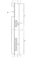
図1〜図3は、従来のMIMキャパシタを製造する方法を示す概略的な断面図である。特に、図1は集積回路基板1のチップ領域Cとスクライブ領域Sを示している。図1に示すように、層間絶縁膜(ILD)3がチップ領域C及びスクライブ領域Sの集積回路基板1上に形成される。層間絶縁膜3は、チップ領域Cの下部金属膜5a及びスクライブ領域Sの金属膜5bを含む。チップ領域の下部金属膜5aは前記MIMキャパシタの下部電極とすることができる一方、スクライブ領域の金属膜5bは第1整列キーK1とすることができる。下部金属膜5a及び金属膜5bは銅を含む材料から形成することができる。
1 to 3 are schematic cross-sectional views showing a method for manufacturing a conventional MIM capacitor. In particular, FIG. 1 shows a chip area C and a scribe area S of the
下部金属膜5aと金属膜5bとを含む層間絶縁膜3上に誘電膜7が形成される。感光膜物質が誘電膜7上に形成されてパターニングされ、内部に開口部9kを含む誘電膜7上に第1フォトレジストパターン9を設ける。
A
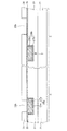
図2に示すように、スクライブ領域S内の層間絶縁膜3の一部は、第1フォトレジストパターン9を用いてエッチングされてスクライブ領域Sに第2整列キーK2を形成する。そして、上部金属膜11及びハードマスク膜13が誘電膜7上に形成され、第2整列キーK2内にコンフォーマルに(conformally)形成される。第2感光膜物質はハードマスク膜13上に形成され、パターニングされて第2フォトレジストパターン15を設ける。
As shown in FIG. 2, a part of the
図3に示すように、第2フォトレジストパターン15は第2フォトレジストパターン15のすぐ下の部分を除いて外側に位置するハードマスク膜13及び上部金属膜11の一部を除去するために用いられ、これによって上部金属電極11a及びハードマスクパターン13aを第2フォトレジストパターン15に形成して図3に示したようなMIM型のキャパシタ構造物が提供される。
As shown in FIG. 3, the
上述の従来技術において、誘電膜7は、第2整列キーK2を形成するために第1フォトレジストパターン9と直接接触している。したがって、誘電膜7が第1フォトレジストパターン9により汚染されてMIMキャパシタの特性を低下させるという問題がある。このような問題を解決するために、第1フォトレジストパターン9は、上部金属膜11を形成した後に形成しなければならない。しかし、このような場合、上部金属膜11は集積回路基板1の全面、特に、スクライブ領域Sの全体にかけて平坦な表面を有するように形成される。この結果、スクライブ領域S内のすべての整列キーが前記平坦な上部金属膜11で覆われる。結果的に、第1フォトレジストパターン9を形成するための写真工程の間に、前記平坦な上部金属膜11はスクライブ領域S内の整列キーが認識されることを防止する。
In the above-described prior art, the
さらに、上述の従来技術によると、下部金属膜5a、すなわち、銅膜から成長するヒルロック(hillocks:図3の5h)が生成する。このような場合、誘電膜7の漏洩電流特性が低下されることもあるし、誘電膜7内にクラック(cracks)が発生することもある。
Furthermore, according to the above-described prior art, the
このようなMIM型のキャパシタは、例えば特許文献1〜特許文献3によって開示されている。
本発明は、上記問題を解決するために成されたものであり、金属電極のヒルロック及びフォトレジスト膜の汚染を防止することができるMIMキャパシタの製造方法を提供することを目的とする。 The present invention has been made to solve the above-described problems, and an object of the present invention is to provide a method for manufacturing an MIM capacitor capable of preventing hilllock of metal electrodes and contamination of a photoresist film.
前記目的を達成するために本発明に係るMIMキャパシタの誘電膜形成方法は、チップ領域およびスクライブ領域を有する集積回路の基板上に、下部導電性プラグが形成された下部層間絶縁膜を形成する段階と、前記下部層間絶縁膜上に下部キャッピング絶縁膜を形成する段階と、前記下部キャッピング絶縁膜上に、前記チップ領域内において前記下部キャッピング絶縁膜を露出させる第1開口部と、前記スクライブ領域内において前記下部キャッピング絶縁膜を露出させる第2開口部と、を有する第1フォトレジストパターンを形成する段階と、前記第1開口部によって露出された前記下部キャッピング絶縁膜を除去して前記下部導電性プラグの表面を露出するとともに、前記第2開口部によって露出された前記下部キャッピング絶縁膜を除去して前記下部層間絶縁膜内にリセスを形成する段階と、前記第1フォトレジストパターンを除去する段階と、前記下部キャッピング絶縁膜の上部、表面が露出された前記下部導電性プラグの上部、および前記リセス内に、下部金属膜、キャパシタ誘電膜、および上部金属膜を順次に形成する段階と、前記上部金属膜上に上部キャッピング絶縁膜を形成する段階と、前記上部キャッピング絶縁膜上に第2フォトレジストパターンを形成する段階と、前記第2フォトレジストパターンの外側に位置する前記上部キャッピング絶縁膜および前記上部金属膜を除去して前記キャパシタ誘電膜を露出させる段階と、前記第2フォトレジストパターンを除去する段階と、全面的にパッシベーション膜を形成する段階と、を含む。 In order to achieve the above object, a method for forming a dielectric film of an MIM capacitor according to the present invention includes forming a lower interlayer insulating film having a lower conductive plug on a substrate of an integrated circuit having a chip region and a scribe region. Forming a lower capping insulating film on the lower interlayer insulating film; a first opening exposing the lower capping insulating film in the chip region on the lower capping insulating film; and in the scribe region Forming a first photoresist pattern having a second opening exposing the lower capping insulating layer, and removing the lower capping insulating layer exposed by the first opening to form the lower conductive layer. The lower capping insulating film exposed by the second opening is exposed to the surface of the plug. Forming a recess in the lower interlayer insulating layer; removing the first photoresist pattern; an upper portion of the lower capping insulating layer; an upper portion of the lower conductive plug having a surface exposed; And sequentially forming a lower metal film, a capacitor dielectric film, and an upper metal film in the recess, forming an upper capping insulating film on the upper metal film, and forming a second metal layer on the upper capping insulating film. Forming a second photoresist pattern; removing the upper capping insulating film and the upper metal film located outside the second photoresist pattern to expose the capacitor dielectric film; and the second photoresist The method includes a step of removing the pattern and a step of forming a passivation film on the entire surface.
また、本発明に係るMIMキャパシタの誘電膜形成方法では、前記下部導電性プラグは、拡散防止膜および金属プラグを含む。 Further, the dielectric film forming method of the MIM capacitor in accordance with the present invention, the lower conductive plug comprises a diffusion preventing film and the metal plug.
また、本発明に係るMIMキャパシタの誘電膜形成方法では、前記下部金属膜は、窒化チタン(TiN)または窒化タンタル(TaN)を含む。 Further, the dielectric film forming method of the MIM capacitor in accordance with the present invention, the lower metal layer comprises titanium nitride (TiN) or tantalum nitride (TaN).
また、本発明に係るMIMキャパシタの誘電膜形成方法では、前記キャパシタ誘電膜は、シリコン窒化物(SiN)、酸化物−窒化物−酸化物(ONO)、または高誘電率(highK)の誘電物質を含む。 Further, the dielectric film forming method of the MIM capacitor in accordance with the present invention, the capacitor dielectric film, a silicon nitride (SiN), oxides - Dielectric oxide (ONO), or a high dielectric constant (highK) - nitride Contains substances.
また、本発明に係るMIMキャパシタの誘電膜形成方法では、前記上部金属膜は、窒化チタン(TiN)または窒化タンタル(TaN)を含む。
Further, the dielectric film forming method of the MIM capacitor in accordance with the present invention, the upper metal layer comprises titanium nitride (TiN) or tantalum nitride (TaN).
また、本発明に係るMIMキャパシタの誘電膜形成方法では、前記上部キャッピング絶縁膜は、シリコン窒化物を含む。 Further, the dielectric film forming method of the MIM capacitor in accordance with the present invention, the upper capping insulating layer comprises silicon nitride.
また、本発明に係るMIMキャパシタの誘電膜形成方法では、前記第2フォトレジストパターンの一部は、前記チップ領域内において前記下部導電性プラグからオフセットされる。また、前記第2フォトレジストパターンの一部は、前記スクライブ領域内において前記リセスと整列される。 Further, the dielectric film forming method of the MIM capacitor in accordance with the present invention, the portion of the second photoresist pattern is offset from the lower conductive plug in said chip region. In addition, a portion of the second photoresist pattern is aligned with the recess in the scribe region.
また、本発明に係るMIMキャパシタの誘電膜形成方法では、前記パッシベーション膜は、シリコン窒化物を含む。 Further, the dielectric film forming method of the MIM capacitor in accordance with the present invention, the passivation layer comprises silicon nitride.
また、本発明に係るMIMキャパシタの誘電膜形成方法は、前記パッシベーション膜上に第1上部層間絶縁膜を形成する段階と、前記第1上部層間絶縁膜上にエッチング阻止膜を形成する段階と、前記エッチング阻止膜上に第2上部層間絶縁膜を形成する段階と、をさらに含む。 The method for forming a dielectric film of an MIM capacitor according to the present invention includes a step of forming a first upper interlayer insulating film on the passivation film, a step of forming an etching stopper film on the first upper interlayer insulating film, Forming a second upper interlayer insulating layer on the etch stop layer.
本発明では、前記MIMキャパシタを形成するのに用いられるフォトレジストパターンから誘電膜を分離するパッシベーション膜が形成されるようにしている。この結果、前記フォトレジスト物質と前記誘電膜が直接接触することを避けられるので、前記フォトレジスト物質が前記誘電膜を汚染する可能性を少なくすることができる。 In the present invention, a passivation film for separating the dielectric film from the photoresist pattern used to form the MIM capacitor is formed. As a result, direct contact between the photoresist material and the dielectric film can be avoided, so that the possibility that the photoresist material contaminates the dielectric film can be reduced.
以下、添付した図面を参照しながら本発明の好適な実施形態を詳細に説明する。なお、本発明は、以下に説明する実施形態に限られることはなく、多様な修正、変更をすることができる。また、図面において、膜及び領域のサイズは、本発明の明確性をあたえるために誇張して示されたものである。なお、本明細書において、要素または膜が、他の要素または膜「上に」、「に接続された」、または「に結合された」と記載される場合、これは他の要素または膜の上に直接存在したり、接続されたり、結合することができ、または介在要素または膜が存在することもできる。これに反して、要素または膜が、他の要素または膜「直上に」、「に直接接続された」、または「に直接結合された」と記載される場合、いかなる介在要素または膜も存在しない。明細書全体にわたって同じ参照番号は、同じ構成要素を示す。本明細書における「及び/または」の用語は、それに係わる項目の少なくとも1つあるもの、及びそれらのあらゆる組合せを含む意味である。 Hereinafter, preferred embodiments of the present invention will be described in detail with reference to the accompanying drawings. The present invention is not limited to the embodiments described below, and various modifications and changes can be made. In the drawings, the sizes of the films and regions are exaggerated for the sake of clarity of the present invention. In this specification, when an element or film is described as “on”, “connected to”, or “coupled to” another element or film, There can be directly on, connected to, coupled to, or intervening elements or membranes. On the other hand, if an element or membrane is described as “directly on”, “directly connected to” or “directly coupled to” another element or membrane, there are no intervening elements or membranes present. . Like reference numerals refer to like elements throughout the specification. As used herein, the term “and / or” is meant to include at least one of the associated items, and any combination thereof.
また、「第1、第2、第3・・・」の用語が多様な要素、構成要素、領域、膜、及び/またはセクションを説明するために明細書に用いているが、要素、構成要素、領域、膜、及び/またはセクションはこれらの用語に限定されることはない。これらの用語は、単に1つの要素、構成要素、領域、膜、及び/またはセクションと区分するために用いているものである。よって、後述する第1要素、構成要素、領域、膜、及び/またはセクションは、本発明の趣旨を逸脱しない範囲で、第2要素、構成要素、領域、膜及び/またはセクションとして用いることができる。 Also, the term “first, second, third...” Is used in the specification to describe various elements, components, regions, films, and / or sections. , Regions, films, and / or sections are not limited to these terms. These terms are only used to distinguish one element, component, region, membrane, and / or section. Accordingly, the first element, component, region, film, and / or section described later can be used as the second element, component, region, film, and / or section without departing from the spirit of the present invention. .
相対的な空間用語、例えば「直下」、「下側」、「下部」、「上側」、及び「上部」などは、明細書で説明の容易性のために図示されているように1つの要素、または特徴部の他の要素及び特徴部に対する対応関係を説明するのに用いられる。これらの相対的な空間用語は、図面に表現されたオリエンテーションのみではなく、使用や動作の際に前記素子の他のオリエンテーションも含むものと理解されなければならない。例えば、図面において前記素子が逆になっていれば、他の要素または特徴部の「下側」、または「直下」に表現された要素は他の要素または特徴部の「上側」を向けることになる。よって、「下側」という代表用語は、上側と下側のオリエンテーションのすべてを含むことができる。前記素子は他の向きで向かうことができ(90度、または他の方向に回転されることができ)、本明細書に用いる相対的な空間用語はこのように解釈されることができる。 Relative spatial terms, such as “directly”, “lower”, “lower”, “upper”, “upper”, etc., refer to one element as illustrated for ease of explanation in the specification. Or a correspondence relationship with other elements and features of the feature. These relative spatial terms should be understood to include not only the orientation depicted in the drawings, but also other orientations of the element in use and operation. For example, if the elements are reversed in the drawing, an element expressed “under” or “directly” of another element or feature is directed to the “upper side” of the other element or feature. Become. Thus, the representative term “lower” can include all of the upper and lower orientations. The elements can be oriented in other orientations (90 degrees or can be rotated in other directions), and the relative spatial terms used herein can be interpreted in this way.
用語の「外側(outside)」は、誘電膜のような下地膜の一部がフォトレジストパターンのような上部構造物によって覆われないものを意味する。 The term “outside” means that a portion of a base film such as a dielectric film is not covered by a superstructure such as a photoresist pattern.
本明細書に用いられた前記用語は、特定の実施形態のみを説明する目的として用いられるもので、本発明を制限するものではない。 本発明の実施形態は、本発明の理想的な実施形態及び中間構造を概略的に例示した断面図を参照しながら説明している。よって、本発明の実施形態は単に例示したものであり、明細書に示す実施形態に制限されると解釈してはならない。これは、例えば製造による形態の変形例を含むことができることを意味し、具体的には、長方形として例示された注入領域は、注入領域から非注入領域への二重変化と言うよりは、むしろその端に丸状、または曲状及び/または注入濃度の傾きを有するのが通常である。よって、図面に示された前記領域は事実上概略的なものである。これらの形態は、素子の実際領域の形態を示したものではなく本発明の範囲を制限するためのものでもない。 The terminology used herein is for the purpose of describing particular embodiments only and is not intended to be limiting of the invention. Embodiments of the present invention are described with reference to cross-sectional views schematically illustrating ideal embodiments and intermediate structures of the present invention. Accordingly, the embodiments of the present invention are illustrative only and should not be construed as limited to the embodiments set forth in the specification. This means that, for example, variations in form due to manufacturing can be included, and in particular, an implanted region illustrated as a rectangle is rather than a double change from an implanted region to a non-implanted region. It usually has a round or curved shape and / or a gradient of the injection concentration at its end. Thus, the regions shown in the drawings are schematic in nature. These forms do not show the form of the actual region of the element, nor are they intended to limit the scope of the present invention.
また、他に定義がなされていない限り、明細書で用いられるすべての用語(技術及び科学用語を含み)は本発明の当業者により通常理解される用語と等しい意味を有する。また、明細書に明示的に定義されていない用語は、理想的また形式的な意味として解釈されるべきではない。 Also, unless otherwise defined, all terms used in the specification (including technical and scientific terms) have the same meaning as commonly understood by one of ordinary skill in the art of the present invention. Also, terms not explicitly defined in the specification should not be construed as ideal or formal meanings.
以下、本発明の好適な一実施形態について詳細に説明する。なお、公知の方法、例えば、エッチングの方法、構成要素の形成方法、積層方法、パターニング方法は、従来の公知の方法を採用することができるので、詳細な説明は省略する。 Hereinafter, a preferred embodiment of the present invention will be described in detail. In addition, since a well-known method can be employ | adopted for a well-known method, for example, the etching method, the formation method of a component, the lamination | stacking method, and the patterning method, detailed description is abbreviate | omitted.
既に述べたように、フォトレジストパターンがキャパシタ誘電体と直接接触することになれば(例えば、図1〜図3に示した配列)、フォトレジストはキャパシタ誘電体を汚染することになる。さらに、前記キャパシタの下部電極がヒルロック(hillocks)を含むように形成されると、誘電膜上に亀裂が(ヒルロックによって)形成される場合にこれらのヒルロックは漏洩電流を増加させることができる。よって、本発明の実施形態では、パッシベーション膜が形成されてMIMキャパシタを形成するために用いられたフォトレジストパターンから誘電膜を分離させる。したがって、前記フォトレジストと前記誘電膜との間の直接接触は避けられることができるし、これは前記フォトレジストが前記誘電膜を汚染する可能性を減少させることができる。また、前記MIMキャパシタの前記上部電極は下部導電性プラグと下部電極との間の界面からオフセットされた状態に形成される。前記界面から前記上部電極をオフセットさせると、前記界面からオフセットされた前記上部電極及び下部電極の対向面を形成することによって漏洩電流(ヒルロックが形成された場合)が減少させることができる。このようにすることで、前記下部導電性プラグ内のヒルロックが、例えば前記界面直上側の前記誘電膜内に亀裂を誘発させると、前記上部及び下部電極の対向面が前記界面から離れた(オフセットされた)状態に形成されているので漏洩電流の増加は観察することができない。 As already mentioned, if the photoresist pattern comes into direct contact with the capacitor dielectric (eg, the arrangement shown in FIGS. 1-3), the photoresist will contaminate the capacitor dielectric. Further, when the lower electrode of the capacitor is formed to include hilllocks, these hilllocks can increase leakage current when cracks are formed on the dielectric layer (by hilllocks). Therefore, in the embodiment of the present invention, the passivation film is formed to separate the dielectric film from the photoresist pattern used for forming the MIM capacitor. Thus, direct contact between the photoresist and the dielectric film can be avoided, and this can reduce the likelihood that the photoresist will contaminate the dielectric film. Further, the upper electrode of the MIM capacitor is formed in an offset state from the interface between the lower conductive plug and the lower electrode. When the upper electrode is offset from the interface, leakage current (when hillocks are formed) can be reduced by forming opposing surfaces of the upper electrode and the lower electrode that are offset from the interface. In this way, when the hilllock in the lower conductive plug induces a crack in the dielectric film immediately above the interface, for example, the opposing surfaces of the upper and lower electrodes are separated from the interface (offset). The increase in leakage current cannot be observed.
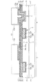
図4は、本発明の一実施形態によるMIMキャパシタ61の平面図である。図4を参照すれば、MIMキャパシタ61は集積回路基板のチップ領域C内に形成される。前記集積回路のスクライブ領域S内にトレンチT及び整列キーKが形成される。MIMキャパシタ61は下部導電性プラグ28aと下部導電性電極31aとに結合されたコンタクト29hを含む。上部導電性電極35aは上部配線54と電気的に結合されるビアホール45v直下の下部導電性電極31a上側に形成される。
FIG. 4 is a plan view of the
図5に示すように、チップ領域C及びスクライブ領域Sにおいて、集積回路の基板21上に下部層間絶縁膜(ILD)23が形成される。チップ領域Cの下部層間絶縁膜23内に下部導電性プラグ28aが形成され、スクライブ領域Sの下部層間絶縁膜23内に金属パターン28bが形成される。下部導電性プラグ28aは層間絶縁膜23にリセスを埋め込む拡散防止膜25a及び金属プラグ27aを含むことができる。金属パターン28bは、拡散防止膜25b及び金属プラグ27bを含むことができる。
As shown in FIG. 5, in the chip region C and the scribe region S, a lower interlayer insulating film (ILD) 23 is formed on the
また、導電性プラグ28aはダマシン工程を用いて形成することができる。スクライブ領域S内に下部導電性プラグ28a及び金属パターン28bを含む層間絶縁膜23上に下部キャッピング絶縁膜29が形成される。
The
さらに図5に示すように、前記集積回路のチップ領域Cとスクライブ領域Sの両方のキャッピング絶縁膜29上に第1フォトレジスト物質が形成される。第1フォトレジスト物質はパターニングされてチップ領域C内の下部導電性プラグ28a上側の第1開口部30hとスクライブ領域S内に第2開口部30kとを有した第1フォトレジストパターン30を形成する。
Further, as shown in FIG. 5, a first photoresist material is formed on the
図6を参照すれば、下部キャッピング絶縁膜29の一部が第1開口部30h及び第2開口部30kを有した第1フォトレジストパターン30によって除去された後、第1フォトレジストパターン30は、下部キャッピング絶縁膜29から除去される。図6に示すように、チップ領域Cでは、下部キャッピング絶縁膜29が除去されてチップ領域C内の導電性プラグ28aの表面を露出させるとともに、キャッピング絶縁膜29の一部とその下にある層間絶縁膜23の一部はスクライブ領域Sで除去されて内部にリセスKが形成される。
Referring to FIG. 6, after a portion of the lower
図7を参照すれば、下部金属膜31、キャパシタ誘電膜33、及び上部金属膜35がチップ領域C内の導電性プラグ28a上の下部キャッピング絶縁膜29上に、そしてスクライブ領域S内のリセスK内に順次に形成される。下部金属膜31は窒化チタン(TiN)、窒化タンタル(TaN)などからなる。また、キャパシタ誘電膜33は、例えば、シリコン窒化物(SiN)、酸化物−窒化物−酸化物(ONO)、高誘電率(highK)の誘電物質などからなる。また、上部金属膜35は金属窒化物、例えば、窒化チタン(TiN)、窒化タンタル(TaN)などのような膜とすることができる。
Referring to FIG. 7, the
図7を参照すれば、チップ領域C及びスクライブ領域S内の上部金属膜35上に上部キャッピング絶縁膜37が形成される。上部キャッピング絶縁膜37はシリコン窒化物の上部金属膜35に対して高いエッチング選択比を有するように選択された物質からなっている。第2フォトレジスト物質が上部キャッピング絶縁膜37上に形成されてパターニングされ、チップ領域C内の一部39a及びスクライブ領域S内の一部39bを含む第2フォトレジストパターン39を形成する。
Referring to FIG. 7, an upper capping insulating film 37 is formed on the upper metal film 35 in the chip region C and the scribe region S. The upper capping insulating film 37 is made of a material selected to have a high etching selectivity with respect to the upper metal film 35 of silicon nitride. A second photoresist material is formed on the upper capping insulating film 37 and patterned to form a
さらに図7に示すように、第2フォトレジストパターン39aの一部は導電性プラグ28aと下部金属膜31との間の界面からオフセットされている。よって、ヒルロックが導電性プラグ28aと下部金属膜31との間の界面に形成されても、上部金属膜31及び下部金属膜35の表面が(順次に形成されて上部及び下部金属電極を設ける。)前記界面からオフセットされることによって、キャパシタの電極を亀裂させる誘電膜33の一部から分離されるので、誘電膜33内の亀裂は従来技術で見られたほどの漏洩電流に影響を及ぼさないものである。
Further, as shown in FIG. 7, a part of the
図8を参照すれば、本発明の一実施形態では、第2フォトレジストパターン39a外側に位置する(第2フォトレジストパターン39直下ではない。)上部キャッピング絶縁膜37の一部とこれらの下にある上部金属膜35の一部が除去されてチップ領域C内の第2フォトレジストパターン39a外側に位置する誘電膜33の表面を露出させる。
Referring to FIG. 8, in an embodiment of the present invention, a part of the upper capping insulating film 37 located outside the
同様に、第2フォトレジストパターン39a外側の上部キャッピング絶縁膜37の一部と上部金属膜35の下部一部が除去されてスクライブ領域S内の第2フォトレジストパターン39b外側に位置する誘電膜33の表面を露出させる。次に、第2フォトレジストパターン39を除去することができる。
Similarly, a part of the upper capping insulating film 37 outside the
本発明の他の実施形態では、第2フォトレジストパターン39aは、マスクとして用いられてチップ領域C及びスクライブ領域Sの両方で第2フォトレジストパターン39外側に位置する上部キャッピング絶縁膜37の一部を除去し、これによって第1上部キャッピング絶縁パターン37a及び第2上部キャッピング絶縁パターン37bがそれぞれ形成される。その後、第2フォトレジストパターン39は除去されることができ、その結果、第1上部キャッピング絶縁パターン37a及び第2上部キャッピング絶縁パターン37bは、第1上部キャッピング絶縁パターン37a及び第2上部キャッピング絶縁パターン37bの外側に位置する上部金属膜35の一部を除去してチップ領域Cに上部金属電極35aとスクライブ領域Sとに上部整列キー35bを形成するように用いられることができる。
In another embodiment of the present invention, the
さらに、図8に示したように、パッシベーション膜41は、チップ領域C及びスクライブ領域S内の誘電膜33の露出された一部上に形成され、導電性プラグ28a直上側からチップ領域C内の上部金属電極35a及びキャッピング絶縁パターン37aまで延長される。同様に、パッシベーション膜41はスクライブ領域S内の金属パターン28b直上側から延長させて、スクライブ領域SのリセスK内の第2上部キャッピング絶縁膜37b及び上部整列キー35bにコンフォーマル(conformal)に形成される。
Further, as shown in FIG. 8, the
したがって、図8に示すようにパッシベーション膜41は、その下に位置する誘電膜33をパッシベーション膜41上に順次に形成されたフォトレジストパターンと直接接触させないように分離させ、これによって前記フォトレジストパターンによる前記誘電体の汚染可能性を少なくすることができる。パッシベーション膜41は、また、上部金属電極35a及びキャパシタ誘電体の側面に対するエッチング損傷により誘発される前記上部金属電極35a及び下部金属電極間の漏洩電流を低減することができる。本発明の一実施形態では、パッシベーション膜41は、シリコン窒化膜である。
Therefore, as shown in FIG. 8, the
図8に示したように、第3フォトレジスト物質がパッシベーション膜41に形成され、パターニングされてチップ領域C内の下部電極パターン43a及びスクライブ領域S内の下部整列キーパターン43bを含む第3フォトレジストパターン43を形成する。
As shown in FIG. 8, a third photoresist material is formed on the
図8及び図9によると、第3フォトレジストパターン43は、第3フォトレジストパターン43外側に位置する前記パッシベーション膜41、誘電膜33、そして下部電極31のそれぞれの一部を除去するのに用いられ、これによって上部電極35a、誘電膜33a及び下部電極31aを含むMIMキャパシタを形成する。
Referring to FIGS. 8 and 9, the
本発明の実施形態では、上部電極及び下部電極の対向面は導電性プラグ28aと導電性プラグ28a直上側とに位置する(そして、これと直接接触する)前記下部電極の一部との間の前記界面から距離を置いて形成される)。
In an embodiment of the present invention, the opposing surfaces of the upper electrode and the lower electrode are located between the
第1上部層間絶縁膜45、エッチング阻止膜47、及び第2上部層間絶縁膜49を含む上部層間絶縁膜50はチップ領域C内の前記MIMキャパシタ上に、そして、スクライブ領域S内の整列キーK上に形成される。
The upper
図10に示したように、ビアホール45v及びトレンチ領域49tが上部層間絶縁膜50、パッシベーション膜41a、及び上部キャッピング絶縁パターン37aを介して形成されて、例えば、デュアルダマシン工程を用いて、上部電極35aの一部を露出させる。本発明の実施形態では、トレンチ領域47tの形成が、例えば時間制御エッチング(time controlled etching)を用いて他の方式によって適切に制御することができる場合、エッチング阻止膜47は、除去することができる。ビアホール45v及びトレンチ領域49t内に上部配線54が形成され、上部金属配線物質53と、トレンチ領域49t及びビアホール45vに沿って整列する上部拡散防止膜51とを含むことができ、これによって本発明の一実施形態に係るMIM型のキャパシタが完成される。
As shown in FIG. 10, the via
以上、本発明の好ましい実施形態を参照しながら説明したが、これは単に本発明を例示したものであって、当業者は、添付の特許請求範囲に記載された本発明の思想及び領域から逸脱しない範囲で、本発明を多様に修正及び変更させることができる。 Although the present invention has been described with reference to the preferred embodiments, it is merely illustrative of the invention, and those skilled in the art will depart from the spirit and scope of the invention as set forth in the appended claims. The present invention can be variously modified and changed without departing from the scope.
デュアルダマシン工程を用いて集積回路に構造物、すなわち、MIMキャパシタを形成する技術分野に有用である。 It is useful in the technical field of forming a structure, that is, an MIM capacitor in an integrated circuit using a dual damascene process.
28a 下部導電性プラグ、
29h コンタクト、
31a 下部導電性電極、
35a 上部導電性電極、
45v ビアホール、
54 上部配線、
61 MIMキャパシタ、
C チップ領域、
K 整列キー、
S スクライブ領域、
T トレンチ。
28a lower conductive plug,
29h contact,
31a Lower conductive electrode,
35a upper conductive electrode,
45v beer hall,
54 Upper wiring,
61 MIM capacitor,
C chip area,
K alignment key,
S scribe area,
T trench.
Claims (10)
前記下部層間絶縁膜上に下部キャッピング絶縁膜を形成する段階と、Forming a lower capping insulating film on the lower interlayer insulating film;
前記下部キャッピング絶縁膜上に、前記チップ領域内において前記下部キャッピング絶縁膜を露出させる第1開口部と、前記スクライブ領域内において前記下部キャッピング絶縁膜を露出させる第2開口部と、を有する第1フォトレジストパターンを形成する段階と、A first opening that exposes the lower capping insulating film in the chip region and a second opening that exposes the lower capping insulating film in the scribe region on the lower capping insulating film. Forming a photoresist pattern; and
前記第1開口部によって露出された前記下部キャッピング絶縁膜を除去して前記下部導電性プラグの表面を露出するとともに、前記第2開口部によって露出された前記下部キャッピング絶縁膜を除去して前記下部層間絶縁膜内にリセスを形成する段階と、The lower capping insulating film exposed by the first opening is removed to expose the surface of the lower conductive plug, and the lower capping insulating film exposed by the second opening is removed to remove the lower capping insulating film. Forming a recess in the interlayer insulating film;
前記第1フォトレジストパターンを除去する段階と、Removing the first photoresist pattern;
前記下部キャッピング絶縁膜の上部、表面が露出された前記下部導電性プラグの上部、および前記リセス内に、下部金属膜、キャパシタ誘電膜、および上部金属膜を順次に形成する段階と、Sequentially forming a lower metal film, a capacitor dielectric film, and an upper metal film in the upper portion of the lower capping insulating film, the upper portion of the lower conductive plug whose surface is exposed, and the recess;
前記上部金属膜上に上部キャッピング絶縁膜を形成する段階と、Forming an upper capping insulating layer on the upper metal layer;
前記上部キャッピング絶縁膜上に第2フォトレジストパターンを形成する段階と、Forming a second photoresist pattern on the upper capping insulating layer;
前記第2フォトレジストパターンの外側に位置する前記上部キャッピング絶縁膜および前記上部金属膜を除去して前記キャパシタ誘電膜を露出させる段階と、Removing the upper capping insulating layer and the upper metal layer located outside the second photoresist pattern to expose the capacitor dielectric layer;
前記第2フォトレジストパターンを除去する段階と、Removing the second photoresist pattern;
全面的にパッシベーション膜を形成する段階と、Forming a passivation film over the entire surface;
を含むMIMキャパシタの誘電膜形成方法。A method for forming a dielectric film of an MIM capacitor.
前記第1上部層間絶縁膜上にエッチング阻止膜を形成する段階と、 Forming an etch stop layer on the first upper interlayer insulating layer;
前記エッチング阻止膜上に第2上部層間絶縁膜を形成する段階と、をさらに含む請求項1に記載のMIMキャパシタの誘電膜形成方法。 The method of claim 1, further comprising: forming a second upper interlayer insulating film on the etch stop layer.
Applications Claiming Priority (4)
| Application Number | Priority Date | Filing Date | Title |
|---|---|---|---|
| KR1020050073498A KR100870178B1 (en) | 2005-08-10 | 2005-08-10 | Semiconducotr devices having a metal-insulator-metal capacitor and methods of fabricating the same |
| KR10-2005-0073498 | 2005-08-10 | ||
| US11/413,282 US7749852B2 (en) | 2005-08-10 | 2006-04-28 | Methods of forming metal-insulator-metal (MIM) capacitors with passivation layers on dielectric layers |
| US11/413,282 | 2006-04-28 |
Publications (3)
| Publication Number | Publication Date |
|---|---|
| JP2007049139A JP2007049139A (en) | 2007-02-22 |
| JP2007049139A5 JP2007049139A5 (en) | 2009-09-10 |
| JP5165868B2 true JP5165868B2 (en) | 2013-03-21 |
Family
ID=37851668
Family Applications (1)
| Application Number | Title | Priority Date | Filing Date |
|---|---|---|---|
| JP2006208185A Expired - Fee Related JP5165868B2 (en) | 2005-08-10 | 2006-07-31 | Method for forming a metal-insulator-metal capacitor with a passivation film on a dielectric film |
Country Status (1)
| Country | Link |
|---|---|
| JP (1) | JP5165868B2 (en) |
Families Citing this family (2)
| Publication number | Priority date | Publication date | Assignee | Title |
|---|---|---|---|---|
| JP6149578B2 (en) * | 2013-07-30 | 2017-06-21 | 富士通セミコンダクター株式会社 | Manufacturing method of electronic device |
| JP7272098B2 (en) * | 2019-05-09 | 2023-05-12 | 富士通セミコンダクターメモリソリューション株式会社 | Semiconductor device and method for manufacturing semiconductor device |
Family Cites Families (6)
| Publication number | Priority date | Publication date | Assignee | Title |
|---|---|---|---|---|
| JP3415551B2 (en) * | 2000-03-27 | 2003-06-09 | 日本電気株式会社 | Method for manufacturing semiconductor device |
| JP3956118B2 (en) * | 2002-07-23 | 2007-08-08 | インターナショナル・ビジネス・マシーンズ・コーポレーション | Semiconductor device manufacturing method and semiconductor device |
| JP4037711B2 (en) * | 2002-07-26 | 2008-01-23 | 株式会社東芝 | Semiconductor device having a capacitor formed in an interlayer insulating film |
| KR100505682B1 (en) * | 2003-04-03 | 2005-08-03 | 삼성전자주식회사 | Dual damascene interconnects including metal-insulator-metal capacitor and fabricating method thereof |
| KR100532455B1 (en) * | 2003-07-29 | 2005-11-30 | 삼성전자주식회사 | Method for manufacturing semiconductor device including MIM capacitor and interconnect structure |
| JP2005079513A (en) * | 2003-09-03 | 2005-03-24 | Seiko Epson Corp | Semiconductor device and its manufacturing method |
-
2006
- 2006-07-31 JP JP2006208185A patent/JP5165868B2/en not_active Expired - Fee Related
Also Published As
| Publication number | Publication date |
|---|---|
| JP2007049139A (en) | 2007-02-22 |
Similar Documents
| Publication | Publication Date | Title |
|---|---|---|
| US7749852B2 (en) | Methods of forming metal-insulator-metal (MIM) capacitors with passivation layers on dielectric layers | |
| US7683415B2 (en) | Semiconductor device and method for fabricating the same | |
| US7476922B2 (en) | Logic device having vertically extending metal-insulator-metal capacitor between interconnect layers and method of fabricating the same | |
| US7220652B2 (en) | Metal-insulator-metal capacitor and interconnecting structure | |
| US20050263848A1 (en) | Metal-insulator-metal capacitor having a large capacitance and method of manufacturing the same | |
| US20040207043A1 (en) | Semiconductor device having capacitor formed in multilayer wiring structure | |
| US11088323B2 (en) | Top electrode last scheme for memory cell to prevent metal redeposit | |
| EP1119027B1 (en) | A capacitor for integration with copper damascene structure and manufacturing method | |
| US20020034866A1 (en) | Semiconductor memory device for reducing damage to interlevel dielectric layer and fabrication method thereof | |
| US7508023B2 (en) | Capacitor structure and fabricating method thereof | |
| JP2006157002A (en) | Manufacturing method of capacitor, and manufacturing method of semiconductor device | |
| JP2005026641A (en) | Semiconductor device and method of manufacturing same | |
| JP5165868B2 (en) | Method for forming a metal-insulator-metal capacitor with a passivation film on a dielectric film | |
| KR100385951B1 (en) | Semiconductor memory device having multi-layer storage node contact plug and fabrication method thereof | |
| US7166507B2 (en) | Semiconductor device and method for forming same using multi-layered hard mask | |
| JP2008300489A (en) | Semiconductor device and manufacturing method thereof | |
| JP2007027303A (en) | Semiconductor device and its manufacturing method | |
| US20050020025A1 (en) | Semiconductor device and method of manufacturing the same | |
| US20080057661A1 (en) | Fabricating method of semiconductor device | |
| US20220238638A1 (en) | Method for processing capacitive structure and semiconductor structure | |
| JP2008277434A (en) | Semiconductor device, and manufacturing method thereof | |
| US7531450B2 (en) | Method of fabricating semiconductor device having contact hole with high aspect-ratio | |
| KR20030002872A (en) | Method of forming contacts of semiconductor memory device | |
| JP2006302987A (en) | Semiconductor device and its manufacturing method | |
| KR100539242B1 (en) | System on chip including a DRAM analog device for improving a DRAM capacitance and method for fabricating the same |
Legal Events
| Date | Code | Title | Description |
|---|---|---|---|
| A521 | Written amendment |
Free format text: JAPANESE INTERMEDIATE CODE: A523 Effective date: 20090729 |
|
| A621 | Written request for application examination |
Free format text: JAPANESE INTERMEDIATE CODE: A621 Effective date: 20090729 |
|
| A521 | Written amendment |
Free format text: JAPANESE INTERMEDIATE CODE: A523 Effective date: 20100622 |
|
| A131 | Notification of reasons for refusal |
Free format text: JAPANESE INTERMEDIATE CODE: A131 Effective date: 20120717 |
|
| A977 | Report on retrieval |
Free format text: JAPANESE INTERMEDIATE CODE: A971007 Effective date: 20120719 |
|
| A521 | Written amendment |
Free format text: JAPANESE INTERMEDIATE CODE: A523 Effective date: 20121017 |
|
| TRDD | Decision of grant or rejection written | ||
| A01 | Written decision to grant a patent or to grant a registration (utility model) |
Free format text: JAPANESE INTERMEDIATE CODE: A01 Effective date: 20121204 |
|
| A61 | First payment of annual fees (during grant procedure) |
Free format text: JAPANESE INTERMEDIATE CODE: A61 Effective date: 20121220 |
|
| FPAY | Renewal fee payment (event date is renewal date of database) |
Free format text: PAYMENT UNTIL: 20151228 Year of fee payment: 3 |
|
| R150 | Certificate of patent (=grant) or registration of utility model |
Free format text: JAPANESE INTERMEDIATE CODE: R150 |
|
| LAPS | Cancellation because of no payment of annual fees |