JP5165723B2 - Circuit board and manufacturing method thereof - Google Patents
Circuit board and manufacturing method thereof Download PDFInfo
- Publication number
- JP5165723B2 JP5165723B2 JP2010100677A JP2010100677A JP5165723B2 JP 5165723 B2 JP5165723 B2 JP 5165723B2 JP 2010100677 A JP2010100677 A JP 2010100677A JP 2010100677 A JP2010100677 A JP 2010100677A JP 5165723 B2 JP5165723 B2 JP 5165723B2
- Authority
- JP
- Japan
- Prior art keywords
- layer
- electroless plating
- insulating layer
- resin
- blind via
- Prior art date
- Legal status (The legal status is an assumption and is not a legal conclusion. Google has not performed a legal analysis and makes no representation as to the accuracy of the status listed.)
- Active
Links
- 238000004519 manufacturing process Methods 0.000 title claims description 29
- 238000007772 electroless plating Methods 0.000 claims description 58
- 238000000034 method Methods 0.000 claims description 42
- 239000000758 substrate Substances 0.000 claims description 20
- 238000007747 plating Methods 0.000 claims description 11
- 229910052802 copper Inorganic materials 0.000 claims description 10
- 239000000463 material Substances 0.000 claims description 10
- 229920005989 resin Polymers 0.000 claims description 10
- 239000011347 resin Substances 0.000 claims description 10
- 229920002120 photoresistant polymer Polymers 0.000 claims description 9
- 239000003822 epoxy resin Substances 0.000 claims description 8
- 229920000647 polyepoxide Polymers 0.000 claims description 8
- 229920001187 thermosetting polymer Polymers 0.000 claims description 8
- 229920005992 thermoplastic resin Polymers 0.000 claims description 7
- 238000000576 coating method Methods 0.000 claims description 4
- 238000005553 drilling Methods 0.000 claims description 4
- 239000003365 glass fiber Substances 0.000 claims description 4
- 229920005668 polycarbonate resin Polymers 0.000 claims description 4
- 239000004431 polycarbonate resin Substances 0.000 claims description 4
- 229920001225 polyester resin Polymers 0.000 claims description 4
- 239000004645 polyester resin Substances 0.000 claims description 4
- 229920001721 polyimide Polymers 0.000 claims description 4
- 239000009719 polyimide resin Substances 0.000 claims description 4
- 238000007788 roughening Methods 0.000 claims description 4
- 229910052804 chromium Inorganic materials 0.000 claims description 3
- 238000007641 inkjet printing Methods 0.000 claims description 3
- 239000002184 metal Substances 0.000 claims description 3
- 229910052751 metal Inorganic materials 0.000 claims description 3
- 229910052759 nickel Inorganic materials 0.000 claims description 3
- 229910052709 silver Inorganic materials 0.000 claims description 3
- 229910052718 tin Inorganic materials 0.000 claims description 3
- 239000010949 copper Substances 0.000 description 12
- 239000000654 additive Substances 0.000 description 9
- RYGMFSIKBFXOCR-UHFFFAOYSA-N Copper Chemical compound [Cu] RYGMFSIKBFXOCR-UHFFFAOYSA-N 0.000 description 7
- 238000005530 etching Methods 0.000 description 5
- 239000011810 insulating material Substances 0.000 description 5
- 239000007788 liquid Substances 0.000 description 3
- 239000002861 polymer material Substances 0.000 description 3
- 238000007639 printing Methods 0.000 description 3
- 239000000853 adhesive Substances 0.000 description 2
- 230000001070 adhesive effect Effects 0.000 description 2
- 239000007787 solid Substances 0.000 description 2
- 229920001169 thermoplastic Polymers 0.000 description 2
- 239000004020 conductor Substances 0.000 description 1
- 230000032798 delamination Effects 0.000 description 1
- 238000010438 heat treatment Methods 0.000 description 1
- 238000007654 immersion Methods 0.000 description 1
- 230000002427 irreversible effect Effects 0.000 description 1
- 239000000155 melt Substances 0.000 description 1
- 238000003825 pressing Methods 0.000 description 1
Images


Classifications
-
- H—ELECTRICITY
- H05—ELECTRIC TECHNIQUES NOT OTHERWISE PROVIDED FOR
- H05K—PRINTED CIRCUITS; CASINGS OR CONSTRUCTIONAL DETAILS OF ELECTRIC APPARATUS; MANUFACTURE OF ASSEMBLAGES OF ELECTRICAL COMPONENTS
- H05K3/00—Apparatus or processes for manufacturing printed circuits
- H05K3/38—Improvement of the adhesion between the insulating substrate and the metal
- H05K3/386—Improvement of the adhesion between the insulating substrate and the metal by the use of an organic polymeric bonding layer, e.g. adhesive
- H05K3/387—Improvement of the adhesion between the insulating substrate and the metal by the use of an organic polymeric bonding layer, e.g. adhesive for electroless plating
-
- C—CHEMISTRY; METALLURGY
- C23—COATING METALLIC MATERIAL; COATING MATERIAL WITH METALLIC MATERIAL; CHEMICAL SURFACE TREATMENT; DIFFUSION TREATMENT OF METALLIC MATERIAL; COATING BY VACUUM EVAPORATION, BY SPUTTERING, BY ION IMPLANTATION OR BY CHEMICAL VAPOUR DEPOSITION, IN GENERAL; INHIBITING CORROSION OF METALLIC MATERIAL OR INCRUSTATION IN GENERAL
- C23C—COATING METALLIC MATERIAL; COATING MATERIAL WITH METALLIC MATERIAL; SURFACE TREATMENT OF METALLIC MATERIAL BY DIFFUSION INTO THE SURFACE, BY CHEMICAL CONVERSION OR SUBSTITUTION; COATING BY VACUUM EVAPORATION, BY SPUTTERING, BY ION IMPLANTATION OR BY CHEMICAL VAPOUR DEPOSITION, IN GENERAL
- C23C18/00—Chemical coating by decomposition of either liquid compounds or solutions of the coating forming compounds, without leaving reaction products of surface material in the coating; Contact plating
- C23C18/16—Chemical coating by decomposition of either liquid compounds or solutions of the coating forming compounds, without leaving reaction products of surface material in the coating; Contact plating by reduction or substitution, e.g. electroless plating
- C23C18/1601—Process or apparatus
- C23C18/1633—Process of electroless plating
- C23C18/1646—Characteristics of the product obtained
- C23C18/165—Multilayered product
- C23C18/1653—Two or more layers with at least one layer obtained by electroless plating and one layer obtained by electroplating
-
- H—ELECTRICITY
- H05—ELECTRIC TECHNIQUES NOT OTHERWISE PROVIDED FOR
- H05K—PRINTED CIRCUITS; CASINGS OR CONSTRUCTIONAL DETAILS OF ELECTRIC APPARATUS; MANUFACTURE OF ASSEMBLAGES OF ELECTRICAL COMPONENTS
- H05K2201/00—Indexing scheme relating to printed circuits covered by H05K1/00
- H05K2201/01—Dielectrics
- H05K2201/0104—Properties and characteristics in general
- H05K2201/0129—Thermoplastic polymer, e.g. auto-adhesive layer; Shaping of thermoplastic polymer
-
- H—ELECTRICITY
- H05—ELECTRIC TECHNIQUES NOT OTHERWISE PROVIDED FOR
- H05K—PRINTED CIRCUITS; CASINGS OR CONSTRUCTIONAL DETAILS OF ELECTRIC APPARATUS; MANUFACTURE OF ASSEMBLAGES OF ELECTRICAL COMPONENTS
- H05K2201/00—Indexing scheme relating to printed circuits covered by H05K1/00
- H05K2201/01—Dielectrics
- H05K2201/0137—Materials
- H05K2201/0145—Polyester, e.g. polyethylene terephthalate [PET], polyethylene naphthalate [PEN]
-
- H—ELECTRICITY
- H05—ELECTRIC TECHNIQUES NOT OTHERWISE PROVIDED FOR
- H05K—PRINTED CIRCUITS; CASINGS OR CONSTRUCTIONAL DETAILS OF ELECTRIC APPARATUS; MANUFACTURE OF ASSEMBLAGES OF ELECTRICAL COMPONENTS
- H05K2201/00—Indexing scheme relating to printed circuits covered by H05K1/00
- H05K2201/01—Dielectrics
- H05K2201/0137—Materials
- H05K2201/0154—Polyimide
-
- H—ELECTRICITY
- H05—ELECTRIC TECHNIQUES NOT OTHERWISE PROVIDED FOR
- H05K—PRINTED CIRCUITS; CASINGS OR CONSTRUCTIONAL DETAILS OF ELECTRIC APPARATUS; MANUFACTURE OF ASSEMBLAGES OF ELECTRICAL COMPONENTS
- H05K3/00—Apparatus or processes for manufacturing printed circuits
- H05K3/46—Manufacturing multilayer circuits
- H05K3/4644—Manufacturing multilayer circuits by building the multilayer layer by layer, i.e. build-up multilayer circuits
-
- Y—GENERAL TAGGING OF NEW TECHNOLOGICAL DEVELOPMENTS; GENERAL TAGGING OF CROSS-SECTIONAL TECHNOLOGIES SPANNING OVER SEVERAL SECTIONS OF THE IPC; TECHNICAL SUBJECTS COVERED BY FORMER USPC CROSS-REFERENCE ART COLLECTIONS [XRACs] AND DIGESTS
- Y10—TECHNICAL SUBJECTS COVERED BY FORMER USPC
- Y10T—TECHNICAL SUBJECTS COVERED BY FORMER US CLASSIFICATION
- Y10T29/00—Metal working
- Y10T29/49—Method of mechanical manufacture
- Y10T29/49002—Electrical device making
- Y10T29/49117—Conductor or circuit manufacturing
- Y10T29/49124—On flat or curved insulated base, e.g., printed circuit, etc.
- Y10T29/49126—Assembling bases
-
- Y—GENERAL TAGGING OF NEW TECHNOLOGICAL DEVELOPMENTS; GENERAL TAGGING OF CROSS-SECTIONAL TECHNOLOGIES SPANNING OVER SEVERAL SECTIONS OF THE IPC; TECHNICAL SUBJECTS COVERED BY FORMER USPC CROSS-REFERENCE ART COLLECTIONS [XRACs] AND DIGESTS
- Y10—TECHNICAL SUBJECTS COVERED BY FORMER USPC
- Y10T—TECHNICAL SUBJECTS COVERED BY FORMER US CLASSIFICATION
- Y10T29/00—Metal working
- Y10T29/49—Method of mechanical manufacture
- Y10T29/49002—Electrical device making
- Y10T29/49117—Conductor or circuit manufacturing
- Y10T29/49124—On flat or curved insulated base, e.g., printed circuit, etc.
- Y10T29/49155—Manufacturing circuit on or in base
- Y10T29/49156—Manufacturing circuit on or in base with selective destruction of conductive paths
-
- Y—GENERAL TAGGING OF NEW TECHNOLOGICAL DEVELOPMENTS; GENERAL TAGGING OF CROSS-SECTIONAL TECHNOLOGIES SPANNING OVER SEVERAL SECTIONS OF THE IPC; TECHNICAL SUBJECTS COVERED BY FORMER USPC CROSS-REFERENCE ART COLLECTIONS [XRACs] AND DIGESTS
- Y10—TECHNICAL SUBJECTS COVERED BY FORMER USPC
- Y10T—TECHNICAL SUBJECTS COVERED BY FORMER US CLASSIFICATION
- Y10T29/00—Metal working
- Y10T29/49—Method of mechanical manufacture
- Y10T29/49002—Electrical device making
- Y10T29/49117—Conductor or circuit manufacturing
- Y10T29/49124—On flat or curved insulated base, e.g., printed circuit, etc.
- Y10T29/49155—Manufacturing circuit on or in base
- Y10T29/49165—Manufacturing circuit on or in base by forming conductive walled aperture in base
-
- Y—GENERAL TAGGING OF NEW TECHNOLOGICAL DEVELOPMENTS; GENERAL TAGGING OF CROSS-SECTIONAL TECHNOLOGIES SPANNING OVER SEVERAL SECTIONS OF THE IPC; TECHNICAL SUBJECTS COVERED BY FORMER USPC CROSS-REFERENCE ART COLLECTIONS [XRACs] AND DIGESTS
- Y10—TECHNICAL SUBJECTS COVERED BY FORMER USPC
- Y10T—TECHNICAL SUBJECTS COVERED BY FORMER US CLASSIFICATION
- Y10T428/00—Stock material or miscellaneous articles
- Y10T428/24—Structurally defined web or sheet [e.g., overall dimension, etc.]
- Y10T428/24273—Structurally defined web or sheet [e.g., overall dimension, etc.] including aperture
- Y10T428/24322—Composite web or sheet
Landscapes
- Chemical & Material Sciences (AREA)
- Engineering & Computer Science (AREA)
- Manufacturing & Machinery (AREA)
- Microelectronics & Electronic Packaging (AREA)
- General Chemical & Material Sciences (AREA)
- Chemical Kinetics & Catalysis (AREA)
- Materials Engineering (AREA)
- Mechanical Engineering (AREA)
- Metallurgy (AREA)
- Organic Chemistry (AREA)
- Manufacturing Of Printed Wiring (AREA)
- Printing Elements For Providing Electric Connections Between Printed Circuits (AREA)
Description
本発明は、回路基板およびその製造方法に関するものであり、特に、プロセス性能を向上させることのできる回路基板およびその製造方法に関するものである。 The present invention relates to a circuit board and a manufacturing method thereof, and more particularly to a circuit board capable of improving process performance and a manufacturing method thereof.
現在、微細パターンと高密度を有する回路基板を製造する方法は、セミアディティブ法(semi-additive process, SAP)を用いて、必要な回路層を形成する。セミアディティブ法は、絶縁材料の特性により、層間絶縁フィルム(Ajinomoto build-up film, ABF)のセミアディティブ法と、非ABFのセミアディティブ法の2つのグループに分けられる。 Currently, a method of manufacturing a circuit board having a fine pattern and a high density forms a necessary circuit layer by using a semi-additive process (SAP). The semi-additive method can be divided into two groups according to the characteristics of the insulating material: a semi-additive method of an Ajinomoto build-up film (ABF) and a non-ABF semi-additive method.
ABFの表面が粗くなった後、ABFの上に導電層を直接製造することができる。それから、平版印刷、メッキ、剥離、エッチング等のセミアディティブ工程を行って、微細パターンを有する回路層を形成する。しかし、絶縁材料がABFに限定されるため、製造コストが高い。 After the surface of the ABF becomes rough, a conductive layer can be directly produced on the ABF. Then, a semi-additive process such as lithographic printing, plating, peeling, and etching is performed to form a circuit layer having a fine pattern. However, since the insulating material is limited to ABF, the manufacturing cost is high.
非ABFを使用して製造する方法は、非ABFの表面に薄い銅層を押圧することを含む。それから、平版印刷、メッキ、剥離、エッチング等のセミアディティブ工程を行って、微細パターンを有する回路層を形成する。しかし、薄い銅膜は非ABFに対して接着力が弱いため、非ABFを使用する方法の工程能力は、ABFを使用する方法の工程能力よりも低い。従って、現在のセミアディティブ工程では、ABFのような特定の材料を使用する場合に、メッキ銅を形成する前に尻銅(bottom copper)を形成しなくても、ABFにメッキ銅を形成することができる。また、非ABFを使用する場合は、非ABFに尻銅とメッキ銅の両方を形成することが必要となる。 A method of manufacturing using non-ABF involves pressing a thin copper layer against the surface of the non-ABF. Then, a semi-additive process such as lithographic printing, plating, peeling, and etching is performed to form a circuit layer having a fine pattern. However, thin since copper film is weak adhesive strength to the non ABF, process capability of the method of using non-ABF is lower than process capability of the method of using the ABF. Therefore, in the current semi-additive process, when a specific material such as ABF is used, the plated copper is formed on the ABF without forming the bottom copper before the plated copper is formed. Can do. Further, when non-ABF is used, it is necessary to form both the bottom copper and the plated copper on the non-ABF.
本発明は、プロセス性能を向上させることのできる回路基板およびその製造方法を提供する。 The present invention provides a circuit board capable of improving process performance and a manufacturing method thereof.
本発明は、ABFのような特定の材料を必要としないことにより、製造コストを下げることのできる回路基板およびその製造方法を提供する。 The present invention provides a circuit board and a method for manufacturing the same that can reduce the manufacturing cost by not requiring a specific material such as ABF.
本発明は、以下のステップを有する回路基板の製造方法を提供する。基板の少なくとも1つの表面に誘電層を形成する。誘電層の上に絶縁層を形成する。絶縁層の一部および誘電層の一部を取り除いて、誘電層および絶縁層の中に少なくとも1つのブラインドバイア(blind via)を形成する。ブラインドバイアの側壁および絶縁層の残りの部分の上に無電解メッキ層(electroless plating layer)を形成する。ここで、絶縁層と無電解メッキ層の間の結合力は、誘電層と無電解メッキ層の間の結合力よりも大きい。無電解メッキ層の上にパターン化された導電層をメッキして、無電解メッキ層の一部分を覆う。 The present invention provides a circuit board manufacturing method having the following steps. A dielectric layer is formed on at least one surface of the substrate. An insulating layer is formed on the dielectric layer. A portion of the insulating layer and a portion of the dielectric layer are removed to form at least one blind via in the dielectric layer and the insulating layer. An electroless plating layer is formed on the sidewalls of the blind via and the remaining portion of the insulating layer. Here, the bonding force between the insulating layer and the electroless plating layer is larger than the bonding force between the dielectric layer and the electroless plating layer. A patterned conductive layer is plated on the electroless plating layer to cover a portion of the electroless plating layer.
本発明は、基板と、誘電層と、絶縁層と、無電解メッキ層と、パターン化された導電層とを含む回路基板を提供する。誘電層は、基板の少なくとも1つの表面に配置される。絶縁層は、誘電層の上に配置される。無電解メッキ層は、絶縁層の一部および少なくとも1つのブラインドバイアの側壁を覆う。ここで、ブラインドバイアは、誘電層および絶縁層の中に形成され、絶縁層と無電解メッキ層の間の結合力は、誘電層と無電解メッキ層の結合力よりも大きい。パターン化された導電層は、無電解メッキ層の上、およびブラインドバイアの中に配置される。 The present invention provides a circuit board that includes a substrate, a dielectric layer, an insulating layer, an electroless plating layer, and a patterned conductive layer. The dielectric layer is disposed on at least one surface of the substrate. The insulating layer is disposed on the dielectric layer. The electroless plating layer covers a portion of the insulating layer and the sidewalls of at least one blind via. Here, the blind via is formed in the dielectric layer and the insulating layer, and the bonding force between the insulating layer and the electroless plating layer is larger than the bonding force between the dielectric layer and the electroless plating layer. The patterned conductive layer is disposed on the electroless plating layer and in the blind via.
本発明のある実施形態中、誘電層は、熱硬化性樹脂を含む。 In some embodiments of the invention, the dielectric layer includes a thermosetting resin.
本発明のある実施形態中、誘電層は、エポキシ樹脂またはガラス繊維強化エポキシ樹脂を含む。 In some embodiments of the invention, the dielectric layer comprises an epoxy resin or a glass fiber reinforced epoxy resin.
本発明のある実施形態中、絶縁層は、熱可塑性樹脂を含む。 In an embodiment of the present invention, the insulating layer includes a thermoplastic resin.
本発明のある実施形態中、絶縁層は、ポリカーボネート樹脂、ポリエステル樹脂、またはポリイミド樹脂を含む。 In an embodiment of the present invention, the insulating layer includes a polycarbonate resin, a polyester resin, or a polyimide resin.
本発明のある実施形態中、製造方法は、さらに、誘電層の上に絶縁層を形成するステップの後に、絶縁層に対して表面粗化処理(surface roughening treatment)を行うことを含む。 In an embodiment of the present invention, the manufacturing method further includes performing a surface roughening treatment on the insulating layer after the step of forming the insulating layer on the dielectric layer.
本発明のある実施形態中、絶縁層を形成する方法は、コーティングプロセス(coating process)またはインクジェット印刷プロセス(inkjet printing process)を行うことを含む。 In some embodiments of the present invention, the method of forming an insulating layer includes performing a coating process or an inkjet printing process.
本発明のある実施形態中、少なくとも1つのブラインドバイアを形成する方法は、レーザ穴あけプロセス(laser-drilling process)を行うことを含む。 In some embodiments of the present invention, the method of forming at least one blind via includes performing a laser-drilling process.
本発明のある実施形態中、少なくとも1つのブラインドバイアを形成するステップは、さらに、ブラインドバイアの下に配置された電気接続パッドを露出して、電気接続パッドを基板の表面に配置することを含む。 In certain embodiments of the present invention, the step of forming at least one blind via further includes exposing an electrical connection pad disposed under the blind via and placing the electrical connection pad on a surface of the substrate. .
本発明のある実施形態中、製造方法は、さらに、パターン化された導電層をメッキするステップの前に、無電解メッキ層の上にパターン化されたフォトレジスト層を形成することを含む。 In some embodiments of the present invention, the manufacturing method further includes forming a patterned photoresist layer on the electroless plating layer prior to the step of plating the patterned conductive layer.
本発明のある実施形態中、製造方法は、さらに、パターン化された導電層をメッキするステップの後に、パターン化されたフォトレジスト層およびパターン化された導電層によって覆われていない無電解メッキ層を取り除くことを含む。 In an embodiment of the present invention, the manufacturing method further includes an electroless plating layer not covered by the patterned photoresist layer and the patterned conductive layer after the step of plating the patterned conductive layer. Including removing.
本発明のある実施形態中、無電解メッキ層の材料は、Cu、Ni、Ag、Cr、およびSnから成る群から選ばれた金属である。 In an embodiment of the present invention, the material of the electroless plating layer is a metal selected from the group consisting of Cu, Ni, Ag, Cr, and Sn.
本発明のある実施形態中、パターン化された導電層は、Cuを含む。 In some embodiments of the present invention, the patterned conductive layer includes Cu.
本発明のある実施形態中、基板の表面は、その上に電気接続パッドを有し、パターン化された導電層は、ブラインドバイアを介して電気接続パッドに電気的に接続される。 In some embodiments of the present invention, the surface of the substrate has electrical connection pads thereon, and the patterned conductive layer is electrically connected to the electrical connection pads via blind vias.
以上のように、回路基板およびその製造方法において、誘電層の上に絶縁層を形成し、それから、絶縁層の上に無電解メッキ層を形成する。絶縁層と無電解メッキ層の間の結合力は、誘電層と無電解メッキ層の間の結合力よりも大きいため、プロセス性能が向上する。 As described above, in the circuit board and the manufacturing method thereof, the insulating layer is formed on the dielectric layer, and then the electroless plating layer is formed on the insulating layer. Since the bonding force between the insulating layer and the electroless plating layer is larger than the bonding force between the dielectric layer and the electroless plating layer, the process performance is improved.
本発明の上記及び他の目的、特徴、および利点をより分かり易くするため、図面と併せた幾つかの実施形態を以下に説明する。 In order to make the above and other objects, features and advantages of the present invention more comprehensible, several embodiments accompanied with figures are described below.
以下、本発明の好ましい実施形態を添付の図面を参照してさらに詳細に説明する。各図面および関連説明において、同一または類似する構成要素には、同一の参照番号を使用する。 Hereinafter, preferred embodiments of the present invention will be described in detail with reference to the accompanying drawings. In the drawings and the related description, the same reference numerals are used for the same or similar components.
図1A〜1Fは、本発明の実施形態に係る回路基板の製造方法の断面図を概略的に示したものである。図2は、本発明の実施形態に係る回路基板の断面図を概略的に示したものである。 1A to 1F schematically show cross-sectional views of a circuit board manufacturing method according to an embodiment of the present invention. FIG. 2 schematically shows a cross-sectional view of a circuit board according to an embodiment of the present invention.
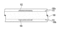
回路基板の製造方法は、以下のステップを含む。図1Aを参照すると、基板100の2つの表面100aおよび100bに、誘電層110を形成する。基板100は、相互に積層された複数のパターン化された回路層(図示せず)および複数のパターン化された誘電層(図示せず)を含む回路板、または他の絶縁材料によって形成されたキャリアである。基板100の表面100aおよび100bは、その上に、それぞれ電気接続パッド102およびパターン化された回路104を有する。電気接続パッド102およびパターン化された回路104は、例えば、Cuを含む。誘電層110は、例えば、熱硬化性樹脂でもよい。基板100の1つの表面に半硬化プリプレグ(semi-cured prepreg)を塗布し、硬化温度(hardening temperature)まで加熱して、流体の変形特性(fluid-deformation property)を有する半硬化プリプレグを硬化した誘電層になるまで硬化する。誘電層110は、初期液体状態のエポキシ樹脂またはガラス繊維強化エポキシ樹脂、あるいは、初期液体状態の不可逆性高分子材料でもよい。
The circuit board manufacturing method includes the following steps. Referring to FIG. 1A, a
図1Bおよび1Cを参照すると、誘電層110の上に絶縁層120を形成する。絶縁層120の一部および誘電層110の一部を取り除いて、誘電層110および絶縁層120の中に少なくとも1つのブラインドバイアCを形成する。絶縁層120は、熱可塑性樹脂でもよく、その形成方法は、例えば、コーティングプロセスまたはインクジェット印刷プロセスを行うことを含む。したがって、絶縁層120は、加熱されると液状樹脂になるまで軟化され、冷却されると固体状樹脂になるまで硬化される。さらに、絶縁層120が誘電層110の上に形成される前に、誘電層110に対して表面粗化処理を行って、硬化した誘電層110と絶縁層120の間の結合力を増強し、各層の間の剥離を防ぐ。
Referring to FIGS. 1B and 1C, an insulating
少なくとも1つのブラインドバイアCを形成する方法は、例えば、レーザ穴あけプロセスを行うことを含む。レーザ穴あけプロセスの後に、デスミア(desmear)ステップを行って、ブラインドバイアCの中の残留物を取り除く。本実施形態において、レーザで誘電層110および絶縁層120を開けた後、ブラインドバイアCの下に配置された電気接続パッド102が露出する。絶縁層120は、例えば、ポリカーボネート樹脂、ポリエステル樹脂、またはポリイミド樹脂を含む。代わりに、絶縁層120は、例えば、熱可塑性高分子材料でもよい。熱可塑性高分子材料は初期固体状態にあるが、加熱されると溶けて、冷却されると初期状態に戻る。さらに、後のセミアディティブ法のために、誘電層110の上に絶縁層120を形成した後に、絶縁層120に対して表面粗化処理を行う。
The method of forming at least one blind via C includes, for example, performing a laser drilling process. After the laser drilling process, a desmear step is performed to remove residues in blind via C. In this embodiment, after the
図1Dおよび1Eを参照すると、ブラインドバイアCの側壁および絶縁層120の残りの部分の上に無電解メッキ層130を形成する。この無電解メッキ層130の上にパターン化された導電層140をメッキして、無電解メッキ層130の一部分を覆う。注意すべきこととして、絶縁層120は熱可塑性樹脂でもよく、誘電層110は熱硬化性樹脂でもよい。誘電層110の上に無電解メッキ層130を直接形成する場合、無電解メッキ層130は熱硬化性樹脂に対して接着力が弱いため、プロセス性能を上げることができない。本発明では、誘電層110の上に絶縁層120を形成し、それから、絶縁層120の上に無電解メッキ層130を形成する。絶縁層120と無電解メッキ層130の間の結合力は、誘電層110と無電解メッキ層130の間の結合力よりも大きいため、プロセス性能が向上する。本実施形態において、無電解メッキ層130の材料は、例えば、Cu、Ni、Ag、Cr、およびSnから成る群から選ばれた金属である。しかしながら、無電解メッキ層130の材料は、これらに限定されない。
Referring to FIGS. 1D and 1E, an
また、無電解メッキ層130の上にパターン化された導電層140をメッキするステップの前に、無電解メッキ層130の上にパターン化されたフォトレジスト層150を形成し、それから、パターン化されたフォトレジスト層150に覆われていない無電解メッキ層130の上に(すなわち、パターン化されたフォトレジスト層150の開口152の中に)導電材料をメッキして、必要なパターン化された導電層140を形成する。本実施形態において、パターン化された導電層140は、ブラインドバイアCを充填し、ブラインドバイアCの下の電気接続パッド102に電気的に接続される。パターン化された導電層140は、例えば、Cuを含む。
Further, before the step of plating the patterned
図1Fを参照すると、パターン化された導電層140をメッキするステップの後に、パターン化されたフォトレジスト層150およびパターン化された導電層140に覆われていない無電解メッキ層130をさらに取り除いて、回路パターンを有する回路層を形成する。無電解メッキ層130を取り除く方法は、例えば、エッチングプロセスを行うことを含む。エッチングプロセスの後、無電解メッキ層130がエッチングされ、同じ回路パターンを有する無電解メッキ層130aを形成する。上述した実施形態において、基板100の2つの表面に、2つの誘電層110、2つの絶縁層120、および2つの無電解メッキ層130を形成し、両面メッキ(double-side plating)を行って、2つのパターン化された導電層140を同時に形成する。しかしながら、本発明はこれに限定されない。当業者であれば、必要に応じて、上述したプロセスを基板の単面に行っても、または両面に行ってもよいことを理解できるであろう。
Referring to FIG. 1F, after the step of plating the patterned
図2に示すように、回路基板10は、基板100と、2つの誘電層110と、2つの絶縁層120と、2つの無電解メッキ層130aと、2つのパターン化された導電層140とを備える。2つの誘電層110は、それぞれ基板100の2つの対抗する表面100aおよび100bに配置される。2つの絶縁層120は、それぞれ2つの誘電層110の上に配置される。2つの無電解メッキ層130aは、2つの絶縁層120の一部および少なくとも1つのブラインドバイアCの側壁を覆う。ここで、ブラインドバイアCは、誘電層110および対応する絶縁層120の中に形成される。絶縁層120と無電解メッキ層130aの間の結合力は、誘電層110と無電解メッキ層130aの間の結合力よりも大きい。2つのパターン化された導電層140は、2つの無電解メッキ層130aの上、およびブラインドバイアCの中に形成され、回路パターンを有する回路層を形成する。さらに、基板100の表面100aは、その上に電気接続パッド102を有し、対応するパターン化された導電層140は、ブラインドバイアCを介して電気接続パッド102に電気的に接続される。上述した実施形態において、回路基板10は、2つの誘電層110と、2つの絶縁層120と、2つの無電解メッキ層130aと、2つのパターン化された導電層140とを備える。しかしながら、本発明はこれらに限定されない。当業者であれば、必要に応じて、単面構造または両面構造が利用可能であることを理解できるであろう。
As shown in FIG. 2, the
以上のように、回路基板およびその製造方法において、誘電層の上に絶縁層を形成し、それから、絶縁層の上に無電解メッキ層を形成する。絶縁層と無電解メッキ層の間の結合力は、誘電層と無電解メッキ層の間の結合力よりも大きいため、プロセス性能が向上する。本発明の絶縁材料はABFに限定されないため、製造コストが下がる。同様に、本発明の絶縁材料が粗くなった後、無電解メッキプロセスまたは液浸コーティング(immersion coating)プロセスを行うことによって、その上に無電解メッキ層を形成することができる。
それから、平版印刷、メッキ、剥離、エッチング等のセミアディティブ工程を行う。
As described above, in the circuit board and the manufacturing method thereof, the insulating layer is formed on the dielectric layer, and then the electroless plating layer is formed on the insulating layer. Since the bonding force between the insulating layer and the electroless plating layer is larger than the bonding force between the dielectric layer and the electroless plating layer, the process performance is improved. Since the insulating material of the present invention is not limited to ABF, the manufacturing cost is reduced. Similarly, after the insulating material of the present invention becomes rough, an electroless plating layer can be formed thereon by performing an electroless plating process or an immersion coating process.
Then, semi-additive processes such as lithographic printing, plating, peeling, and etching are performed.
以上のごとく、この発明を実施形態により開示したが、もとより、この発明を限定するためのものではなく、当業者であれば容易に理解できるように、この発明の技術思想の範囲内において、適当な変更ならびに修正が当然なされうるものであるから、その特許権保護の範囲は、特許請求の範囲および、それと均等な領域を基準として定めなければならない。 As described above, the present invention has been disclosed by the embodiments. However, the present invention is not intended to limit the present invention, and is within the scope of the technical idea of the present invention so that those skilled in the art can easily understand. Therefore, the scope of patent protection should be defined based on the scope of claims and the equivalent area.
10 回路基板
100 基板
100a、100b 表面
102 電気接続パッド
104 パターン化された回路
110 誘電層
120 絶縁層
130、130a 無電解メッキ層
140 パターン化された導電層
150 パターン化されたフォトレジスト層
152 開口
C ブラインドバイア
DESCRIPTION OF
Claims (11)
前記誘電層の上に絶縁層を形成し、前記絶縁層の材質が熱可塑性樹脂であり、前記熱可塑性樹脂がポリカーボネート樹脂、ポリエステル樹脂、またはポリイミド樹脂であることと、
前記絶縁層の一部および前記誘電層の一部を取り除いて、前記誘電層および前記絶縁層の中に少なくとも1つのブラインドバイアを形成することと、
前記ブラインドバイアの側壁および前記絶縁層の残りの部分の上に無電解メッキ層を形成することと、
前記無電解メッキ層上にパターン化された導電層をメッキして、前記無電解メッキ層の一部分を覆うことと
を含み、前記絶縁層と前記無電解メッキ層の間の結合力が、前記誘電層と前記無電解メッキ層の間の結合力よりも大きい回路基板の製造方法。 Forming a dielectric layer on at least one surface of the substrate , wherein the material of the dielectric layer is a thermosetting resin, and the thermosetting resin is an epoxy resin or a glass fiber reinforced epoxy resin ;
An insulating layer is formed on the dielectric layer, the material of the insulating layer is a thermoplastic resin, and the thermoplastic resin is a polycarbonate resin, a polyester resin, or a polyimide resin ,
Removing a portion of the insulating layer and a portion of the dielectric layer to form at least one blind via in the dielectric layer and the insulating layer;
Forming an electroless plating layer on the side wall of the blind via and the remaining portion of the insulating layer;
Plating a patterned conductive layer on the electroless plating layer and covering a portion of the electroless plating layer, wherein a bonding force between the insulating layer and the electroless plating layer is the dielectric A method of manufacturing a circuit board having a bonding strength between a layer and the electroless plating layer.
前記基板の少なくとも1つの表面に配置され、材質が熱硬化性樹脂であり、前記熱硬化性樹脂がエポキシ樹脂又はガラス繊維強化エポキシ樹脂である誘電層と、
前記誘電層の上に配置され、材質が熱可塑性樹脂であり、前記熱可塑性樹脂がポリカーボネート樹脂、ポリエステル樹脂、またはポリイミド樹脂である絶縁層と、
前記絶縁層の一部および少なくとも1つのブラインドバイアの側壁を覆う無電解メッキ層と、
前記無電解メッキ層の上、および前記ブラインドバイアの中に配置されたパターン化された導電層と
を含み、前記ブラインドバイアが前記誘電層および前記絶縁層の中に形成され、前記絶縁層と前記無電解メッキ層の間の結合力が、前記誘電層と前記無電解メッキ層の間の結合力よりも大きい回路基板。 A substrate,
A dielectric layer disposed on at least one surface of the substrate, wherein the material is a thermosetting resin, and the thermosetting resin is an epoxy resin or a glass fiber reinforced epoxy resin ;
An insulating layer disposed on the dielectric layer, wherein the material is a thermoplastic resin, and the thermoplastic resin is a polycarbonate resin, a polyester resin, or a polyimide resin ;
An electroless plating layer covering a portion of the insulating layer and a sidewall of at least one blind via;
A patterned conductive layer disposed on the electroless plating layer and in the blind via, wherein the blind via is formed in the dielectric layer and the insulating layer, the insulating layer and the insulating layer A circuit board in which a bonding force between electroless plating layers is larger than a bonding force between the dielectric layer and the electroless plating layer.
Applications Claiming Priority (2)
| Application Number | Priority Date | Filing Date | Title |
|---|---|---|---|
| TW098146204 | 2009-12-31 | ||
| TW98146204A TWI471073B (en) | 2009-12-31 | 2009-12-31 | Circuit substrate and manufacturing method thereof |
Publications (3)
| Publication Number | Publication Date |
|---|---|
| JP2011139010A JP2011139010A (en) | 2011-07-14 |
| JP2011139010A5 JP2011139010A5 (en) | 2012-07-05 |
| JP5165723B2 true JP5165723B2 (en) | 2013-03-21 |
Family
ID=44186068
Family Applications (1)
| Application Number | Title | Priority Date | Filing Date |
|---|---|---|---|
| JP2010100677A Active JP5165723B2 (en) | 2009-12-31 | 2010-04-26 | Circuit board and manufacturing method thereof |
Country Status (3)
| Country | Link |
|---|---|
| US (1) | US8247705B2 (en) |
| JP (1) | JP5165723B2 (en) |
| TW (1) | TWI471073B (en) |
Families Citing this family (5)
| Publication number | Priority date | Publication date | Assignee | Title |
|---|---|---|---|---|
| TW201304640A (en) * | 2011-07-08 | 2013-01-16 | Kinsus Interconnect Tech Corp | Manufacturing method of circuit board conductive bumps |
| CN102905474B (en) * | 2011-07-28 | 2015-09-30 | 景硕科技股份有限公司 | The manufacture method of circuit board conductive projection |
| KR20130065216A (en) * | 2011-12-09 | 2013-06-19 | 삼성전기주식회사 | Multi-layered printed circuit board and manufacturing metheod thereof |
| JP6208411B2 (en) * | 2012-06-15 | 2017-10-04 | 新光電気工業株式会社 | Wiring board and manufacturing method thereof |
| CN105491796B (en) * | 2014-10-08 | 2019-02-22 | 深圳市昶东鑫线路板有限公司 | The production method of circuit board |
Family Cites Families (6)
| Publication number | Priority date | Publication date | Assignee | Title |
|---|---|---|---|---|
| IT1256647B (en) | 1992-12-11 | 1995-12-12 | Montecatini Tecnologie Srl | PROCEDURE FOR THE PREPARATION OF (CO) POLYMERS AT WIDE DISTRIBUTION OF MOLECULAR WEIGHTS OF ETHYLENE. |
| TW296436B (en) | 1996-04-09 | 1997-01-21 | Matsushita Electric Ind Co Ltd | |
| JP2004189981A (en) | 2002-12-13 | 2004-07-08 | Kanegafuchi Chem Ind Co Ltd | Thermoplastic polyimide resin material and laminated body, and manufacturing method of printed wiring board |
| TWI253714B (en) * | 2004-12-21 | 2006-04-21 | Phoenix Prec Technology Corp | Method for fabricating a multi-layer circuit board with fine pitch |
| JP2007059689A (en) | 2005-08-25 | 2007-03-08 | Shinko Electric Ind Co Ltd | Laminated structured including glass-cloth containing resin layer, and manufacturing method therefor |
| TWI358979B (en) * | 2008-04-23 | 2012-02-21 | Mutual Tek Ind Co Ltd | Printed circuit board with embedded electronic com |
-
2009
- 2009-12-31 TW TW98146204A patent/TWI471073B/en active
-
2010
- 2010-03-05 US US12/718,226 patent/US8247705B2/en active Active
- 2010-04-26 JP JP2010100677A patent/JP5165723B2/en active Active
Also Published As
| Publication number | Publication date |
|---|---|
| US8247705B2 (en) | 2012-08-21 |
| TW201124026A (en) | 2011-07-01 |
| TWI471073B (en) | 2015-01-21 |
| US20110155427A1 (en) | 2011-06-30 |
| JP2011139010A (en) | 2011-07-14 |
Similar Documents
| Publication | Publication Date | Title |
|---|---|---|
| US9532466B2 (en) | Method of manufacturing multi-layer circuit board and multi-layer circuit board manufactured by using the method | |
| US7937833B2 (en) | Method of manufacturing circuit board | |
| KR100797692B1 (en) | Printed Circuit Board and Fabricating Method of the same | |
| US8356405B2 (en) | Method of manufacturing printed circuit board | |
| US9572250B2 (en) | Printed circuit board and method for manufacturing the same | |
| JP2007324559A (en) | Multilayer circuit board with fine pitch and fabricating method thereof | |
| US20090283302A1 (en) | Printed circuit board and manufacturing method thereof | |
| US11600430B2 (en) | Inductor including high-rigidity insulating layers | |
| JP5165723B2 (en) | Circuit board and manufacturing method thereof | |
| KR100619348B1 (en) | Method for manufacturing package substrate using a electroless Ni plating | |
| US9497853B2 (en) | Printed circuit board and method for manufacturing the same | |
| KR101148735B1 (en) | Printed circuit board and method of manufacturing the same | |
| JP2009283671A (en) | Method of manufacturing printed-wiring board | |
| KR100704920B1 (en) | Pcb and it's manufacturing method used bump board | |
| JP2013135080A (en) | Manufacturing method of multilayer wiring board | |
| US8828247B2 (en) | Method of manufacturing printed circuit board having vias and fine circuit and printed circuit board manufactured using the same | |
| TWI573509B (en) | Method of manufacturing mutli-layer circuit board and mutli-layer circuit board manufactured by using the method | |
| KR101987378B1 (en) | Method of manufacturing printed circuit board | |
| KR101167422B1 (en) | Carrier member and method of manufacturing PCB using the same | |
| KR101067204B1 (en) | A printed circuit board and a fabricating method the same | |
| KR20040061410A (en) | PCB with the plated through holes filled with copper with copper and the fabricating method thereof | |
| JP2013008945A (en) | Manufacturing method of coreless substrate | |
| JP2011222962A (en) | Print circuit board and method of manufacturing the same | |
| US20100193232A1 (en) | Printed circuit board and method of manufacturing the same | |
| JP2009032957A (en) | Printed-circuit board and method for manufacturing the same |
Legal Events
| Date | Code | Title | Description |
|---|---|---|---|
| A131 | Notification of reasons for refusal |
Free format text: JAPANESE INTERMEDIATE CODE: A131 Effective date: 20120227 |
|
| A521 | Request for written amendment filed |
Free format text: JAPANESE INTERMEDIATE CODE: A523 Effective date: 20120511 |
|
| A524 | Written submission of copy of amendment under article 19 pct |
Free format text: JAPANESE INTERMEDIATE CODE: A524 Effective date: 20120511 |
|
| TRDD | Decision of grant or rejection written | ||
| A01 | Written decision to grant a patent or to grant a registration (utility model) |
Free format text: JAPANESE INTERMEDIATE CODE: A01 Effective date: 20121122 |
|
| A61 | First payment of annual fees (during grant procedure) |
Free format text: JAPANESE INTERMEDIATE CODE: A61 Effective date: 20121219 |
|
| FPAY | Renewal fee payment (event date is renewal date of database) |
Free format text: PAYMENT UNTIL: 20151228 Year of fee payment: 3 |
|
| R150 | Certificate of patent or registration of utility model |
Ref document number: 5165723 Country of ref document: JP Free format text: JAPANESE INTERMEDIATE CODE: R150 Free format text: JAPANESE INTERMEDIATE CODE: R150 |
|
| R250 | Receipt of annual fees |
Free format text: JAPANESE INTERMEDIATE CODE: R250 |
|
| R250 | Receipt of annual fees |
Free format text: JAPANESE INTERMEDIATE CODE: R250 |
|
| R250 | Receipt of annual fees |
Free format text: JAPANESE INTERMEDIATE CODE: R250 |
|
| R250 | Receipt of annual fees |
Free format text: JAPANESE INTERMEDIATE CODE: R250 |
|
| R250 | Receipt of annual fees |
Free format text: JAPANESE INTERMEDIATE CODE: R250 |
|
| R250 | Receipt of annual fees |
Free format text: JAPANESE INTERMEDIATE CODE: R250 |
|
| R250 | Receipt of annual fees |
Free format text: JAPANESE INTERMEDIATE CODE: R250 |
|
| R250 | Receipt of annual fees |
Free format text: JAPANESE INTERMEDIATE CODE: R250 |
|
| R250 | Receipt of annual fees |
Free format text: JAPANESE INTERMEDIATE CODE: R250 |