JP5163045B2 - Epitaxial growth substrate manufacturing method and nitride compound semiconductor device manufacturing method - Google Patents
Epitaxial growth substrate manufacturing method and nitride compound semiconductor device manufacturing method Download PDFInfo
- Publication number
- JP5163045B2 JP5163045B2 JP2007268305A JP2007268305A JP5163045B2 JP 5163045 B2 JP5163045 B2 JP 5163045B2 JP 2007268305 A JP2007268305 A JP 2007268305A JP 2007268305 A JP2007268305 A JP 2007268305A JP 5163045 B2 JP5163045 B2 JP 5163045B2
- Authority
- JP
- Japan
- Prior art keywords
- layer
- compound semiconductor
- nitride
- support substrate
- substrate
- Prior art date
- Legal status (The legal status is an assumption and is not a legal conclusion. Google has not performed a legal analysis and makes no representation as to the accuracy of the status listed.)
- Expired - Fee Related
Links
Images


Description
本発明は、エピタキシャル成長基板及び窒化物系化合物半導体素子に関し、特に支持基板上のエピタキシャル成長層の反りやクラックの発生を抑制し、且つ製造リードタイムを比較的短くするするエピタキシャル成長基板の製造方法、窒化物系化合物半導体素子の製造方法、エピタキシャル成長基板及び窒化物系化合物半導体素子に関する。 The present invention relates to an epitaxial growth substrate and a nitride-based compound semiconductor device, and more particularly to a method for manufacturing an epitaxial growth substrate, which suppresses the occurrence of warpage and cracks in an epitaxial growth layer on a support substrate and relatively shortens the manufacturing lead time, and nitride The present invention relates to a method for manufacturing a compound semiconductor device, an epitaxial growth substrate, and a nitride compound semiconductor device.
パワー素子(HEMTやショットキーバリアダイオードなど)、発光ダイオード(LED)等の材料として、ガリウムナイトライド(GaN)、インジウムナイトライド(InN)、アルミナイトライド(AlN)、インジウムガリウムナイトライド(InGaN)、アルミガリウムナイトライド(AlGaN)等の窒化物系化合物半導体を用いるのが一般的である。これらの窒化物系化合物半導体は、サファイア基板、炭化ケイ素(SiC)基板、シリコン(Si)基板等の異種材料の基板を用い、有機金属気相成長(MOVPE)法、分子線結晶成長(MBE)法、ハイドライド気相成長(HVPE)法等の例えば気相エピタキシャル成長法により得ることができる。 Materials such as power elements (HEMT, Schottky barrier diode, etc.), light emitting diodes (LED), gallium nitride (GaN), indium nitride (InN), aluminum nitride (AlN), indium gallium nitride (InGaN) In general, a nitride compound semiconductor such as aluminum gallium nitride (AlGaN) is used. These nitride-based compound semiconductors use substrates of dissimilar materials such as sapphire substrates, silicon carbide (SiC) substrates, silicon (Si) substrates, etc., metal organic chemical vapor deposition (MOVPE) method, molecular beam crystal growth (MBE). For example, vapor phase epitaxy such as hydride vapor phase epitaxy (HVPE).
しかし、エピタキシャル成長等によって形成されるGaN等の窒化物系半導体層とその土台となるSi基板やサファイア基板等の支持基板とでは、格子定数や熱膨張係数に大きな差がある。例えば、シリコン基板に窒化物系半導体層をエピタキシャル成長させた後に反応炉の外部へ取り出すために反応炉を降温すると、支持基板には大きな圧縮応力が働き、エピタキシャル成長層には引っ張り応力が働く。その結果、エピタキシャル成長層にクラックが発生する恐れがある。 However, there is a large difference in lattice constant and thermal expansion coefficient between a nitride-based semiconductor layer such as GaN formed by epitaxial growth or the like and a supporting substrate such as a Si substrate or sapphire substrate serving as the foundation. For example, when a nitride-based semiconductor layer is epitaxially grown on a silicon substrate and then the temperature of the reaction furnace is lowered to take it out of the reaction furnace, a large compressive stress acts on the support substrate, and a tensile stress acts on the epitaxial growth layer. As a result, cracks may occur in the epitaxial growth layer.
そこで、図4に示すように、窒化ケイ素(SiN)のマスクを用いてシリコン基板の上面に台形溝を形成し、台形溝の表面に選択的に半導体膜(シリコン酸化膜)を成長させて半導体膜表面にAlN緩衝層を形成させないようにした後、AlN緩衝層をシリコン基板上面に選択的に形成し、AlN緩衝層上に形成されるGaN層を台形溝上を覆い尽くすように形成することで、エピタキシャル成長基板の反りやクラックの発生を抑制する提案がなされている(例えば、特許文献1参照)。また、サファイア基板の場合、支持基板の上に窒化物系半導体層をエピタキシャル成長した後に降温すると、支持基板には大きな引っ張り応力が働く。その結果、窒化物系化合物半導体層の反りが大きくなり、窒化物系化合物半導体層と支持基板との界面にクラックが発生し、それが窒化物系化合物半導体層内を伝播する恐れがある。そこで、図5に示すように、サファイア基板上にサファイア基板よりもエッチング率が低いAlN層をドット状に形成した後、このAlN層をマスクとしてAlNよりもサファイア基板に対する溶解度が大きいエッチング液にてマスクを完全にエッチングして多硬質バッファ層を形成すると伴にマスクが形成されていないサファイア基板表面領域に穴が形成され、その後にGaN層を穴上を覆い尽くすように形成することで、エピタキシャル成長基板の反りやクラックの発生を抑制する提案がなされている(例えば、特許文献2参照)。 Therefore, as shown in FIG. 4, a trapezoidal groove is formed on the upper surface of the silicon substrate using a silicon nitride (SiN) mask, and a semiconductor film (silicon oxide film) is selectively grown on the surface of the trapezoidal groove, thereby forming a semiconductor. After the AlN buffer layer is not formed on the film surface, the AlN buffer layer is selectively formed on the upper surface of the silicon substrate, and the GaN layer formed on the AlN buffer layer is formed so as to cover the trapezoidal groove. There have been proposals for suppressing warpage and cracking of an epitaxial growth substrate (see, for example, Patent Document 1). In the case of a sapphire substrate, a large tensile stress acts on the support substrate when the temperature is lowered after the nitride-based semiconductor layer is epitaxially grown on the support substrate. As a result, the warpage of the nitride-based compound semiconductor layer increases, and a crack is generated at the interface between the nitride-based compound semiconductor layer and the support substrate, which may propagate through the nitride-based compound semiconductor layer. Therefore, as shown in FIG. 5, after an AlN layer having a lower etching rate than the sapphire substrate is formed on the sapphire substrate in a dot shape, an etching solution having a higher solubility in the sapphire substrate than the AlN is formed using this AlN layer as a mask. When the mask is completely etched to form a multi-hard buffer layer, a hole is formed in the surface area of the sapphire substrate where the mask is not formed, and then the GaN layer is formed so as to cover the hole. Proposals have been made to suppress the occurrence of warpage and cracks in the substrate (for example, see Patent Document 2).
しかしながら、上述した方法では、GaN等を支持基板上にエピタキシャル成長する工程以外に、成膜(蒸着、スパッタ等)工程、フォトリソグラフィ工程、エッチング工程等を行う必要があるので、製造リードタイムの延長を引き起こしてしまう。
本発明は、エピタキシャル成長基板の反りやクラックの発生を抑制し、且つ製造リードタイムを比較的短くすることができるエピタキシャル成長基板の製造方法、窒化物系化合物半導体素子の製造方法、エピタキシャル成長基板及び窒化物系化合物半導体素子を提供することを目的とする。 The present invention relates to an epitaxial growth substrate manufacturing method, a nitride-based compound semiconductor device manufacturing method, an epitaxial growth substrate, and a nitride-based manufacturing method capable of suppressing warpage and cracking of the epitaxial growth substrate and relatively shortening the manufacturing lead time. An object is to provide a compound semiconductor device.
本願発明の一態様によれば、ガリウムと反応して表面に穴を形成するシリコン基板の上面にメルトバックエッチングによる穴と穴の空間を閉じた厚みを有し且つガリウムを含まない第1の窒化物系化合物半導体からなる第1の層を形成する工程と、第1の層が形成された支持基板上にガリウムを含む第2の窒化物系化合物半導体からなる層を気相エピタキシャル成長させる工程とを含むエピタキシャル成長基板の製造方法であることを要旨とする。 According to one aspect of the present invention, the first nitridation has a thickness in which holes and hole spaces are closed by meltback etching on the upper surface of a silicon substrate that reacts with gallium to form holes in the surface and does not contain gallium. A step of forming a first layer made of a physical compound semiconductor, and a step of vapor phase epitaxially growing a layer made of a second nitride based compound semiconductor containing gallium on the support substrate on which the first layer is formed. The gist of the present invention is a method for manufacturing an epitaxial growth substrate.
本願発明の他の態様によれば、ガリウムと反応して表面に穴を形成するシリコン基板の上面にメルトバックエッチングによる穴と穴の空間を閉じた厚みを有し且つガリウムを含まない第1の窒化物系化合物半導体からなる第1の層を形成する工程と、第1の層が形成された支持基板上にガリウムを含む窒化物系化合物半導体からなる第2の層を気相エピタキシャル成長させる工程と、第2の層を介して支持基板上に窒化物系化合物半導体からなる素子形成領域を形成する工程とを含む窒化物系化合物半導体素子の製造方法であることを要旨とする。 According to another aspect of the present invention, the first surface of the silicon substrate , which reacts with gallium to form a hole in the surface, has a thickness in which a hole and a hole space are closed by meltback etching and does not contain gallium. Forming a first layer made of a nitride-based compound semiconductor; and vapor-phase epitaxially growing a second layer made of a nitride-based compound semiconductor containing gallium on the support substrate on which the first layer is formed. And a method of manufacturing a nitride-based compound semiconductor element including a step of forming an element formation region made of a nitride-based compound semiconductor on a support substrate via a second layer.
本発明によれば、エピタキシャル成長基板の反りやクラックの発生を抑制し、且つ製造リードタイムを比較的短くすることができるエピタキシャル成長基板の製造方法、窒化物系化合物半導体素子の製造方法、エピタキシャル成長基板及び窒化物系化合物半導体素子を提供することができる。 According to the present invention, a method of manufacturing an epitaxial growth substrate, a method of manufacturing a nitride-based compound semiconductor device, a method of manufacturing a nitride compound semiconductor device, an epitaxial growth substrate, and a nitride A physical compound semiconductor device can be provided.
以下に図面を参照して、本発明の実施の形態を説明する。以下の図面の記載において、同一又は類似の部分には同一又は類似の符号で表している。但し、図面は模式的なものであり、厚みと平面寸法との関係、各層の厚みの比率等は現実のものとは異なる。したがって、具体的な厚みや寸法は以下の説明を照らし合わせて判断するべきものである。また、図面相互間においても互いの寸法の関係や比率が異なる部分が含まれていることは勿論である。 Embodiments of the present invention will be described below with reference to the drawings. In the following description of the drawings, the same or similar parts are denoted by the same or similar reference numerals. However, the drawings are schematic, and the relationship between the thickness and the planar dimensions, the ratio of the thickness of each layer, and the like are different from the actual ones. Therefore, specific thicknesses and dimensions should be determined in light of the following description. Moreover, it is a matter of course that portions having different dimensional relationships and ratios are included between the drawings.
(実施の形態)
本発明の実施の形態に係るエピタキシャル成長基板及び窒化物系化合物半導体素子の製造方法について、図1を参照しながら説明する。
(Embodiment)
An epitaxial growth substrate and a nitride compound semiconductor device manufacturing method according to an embodiment of the present invention will be described with reference to FIG.
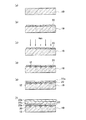
(イ)まず、図1(a)に示すように、ガリウム(Ga)と反応するとメルトバックを生じて表面に穴が形成される材料からなる支持基板10として、例えば、シリコン(Si)基板を採用することができる。支持基板10にSi基板等を採用した場合、支持基板10とガリウム(Ga)が反応するとその支持基板10の表面に合金(アロイ)を形成し、支持基板10の表面に穴を開けるほどの強いエッチング反応(メルトバックエッチング)を生じる。
(A) First, as shown in FIG. 1A, for example, a silicon (Si) substrate is used as a
ちなみに、支持基板10は、例えば350〜1000μmの厚みを有し、バッファ層22及び素子形成領域30(図2及び図3参照)よりも大きい格子定数(例えば、シリコン基板の場合、0.543nm)を有し、且つバッファ層22の線膨張係数(例えば、5.59×10⁻⁶/K)よりも小さい線膨張係数(例えば、4.70×10−6/K)を有する単結晶シリコンからなり、バッファ層22及び素子形成領域30をエピタキシャル成長させるための機能及び機械的支持基板としての機能を有する。
Incidentally, the
(ロ)次に、支持基板の表面の酸化膜を取り除いた後、図1(b)に示すように、支持基板10上に複数のバッファ層成長核20を形成する。バッファ層成長核20は、後述する窒化物系化合物半導体からなる第1の層22aが均一成長する前の段階である。したがって、バッファ層成長核20が設けられていない支持基板10の領域は支持基板10が露出している。バッファ層成長核20は、支持基板10の格子定数に近く、GaNよりも格子定数が小さい第1の窒化物系化合物半導体として、AlN等の3次元成長する結晶を支持基板10の(111)面上に有機金属化学気相蒸着(MOCVD)法等の気相エピタキシャル成長法により支持基板10の温度を1000〜1300℃にして厚み1〜50nm程度の薄い単結晶となるように成長させる。ここで、バッファ層成長核20が多結晶である場合、Gaとバッファ層成長核20が設けられた支持基板10の上面との反応を生じやすくなり、バッファ層成長核20が設けられた支持基板10の上面にも穴12が生じやすくなるためである。なお、この工程において、バッファ層成長核20がドット状又はドット状から更に横方向にも成長して互いのバッファ層成長核20が接続し、互いのバッファ層成長核20の接続した部分がバッファ層成長核20の他の部分よりも薄く形成されていても良い。つまり、ドット状に形成された窒化物系化合物半導体からなるバッファ層成長核20が更に結晶成長して互いのバッファ層成長核20が接合しているが、接合部付近で不均一の厚み繋がっている(特に互いのバッファ層成長核20の接続された上面にピットを有する)初期層でも良い。
(B) Next, after removing the oxide film on the surface of the support substrate, a plurality of buffer
(ハ)次に、図1(c)に示すように、800℃以上の温度、例えば1000℃〜1300℃にて、Gaを含みメチル基を有するトリメチルガリウム(TMG)やGaを含みエチル基を有するトリエチルガリウム(TEG)等とアンモニア(NH3)を水素(H2)もしくは窒素(N2)をキャリアガスとして用いてプリフローする。なお、あまり温度を上げすぎると、Gaが支持基板10と反応しないため、1300度以下とすることが望ましい。また、バッファ層成長核20を構成するAlNは、Si基板に比べて結合エネルギーが強く、AlNが表面に設けられたSi基板の表面は、AlNがメルトバックを生じにくい。したがって、図1(d)に示すように、バッファ層成長核20が設けられておらず、支持基板10が露出している箇所では、トリメチルガリウム(TMG)に含まれるGaと反応して支持基板10にはメルトバックエッチングが生じ、バッファ層成長核20が設けられていない支持基板10の表面に、例えばその深さ方向よりもその横方向に長い異方性の穴が形成されて、支持基板10の上面側に穴12が設けられる。一方、バッファ層成長核20が設けられた支持基板10の上面では、支持基板10の表面とGaとの反応によるメルトバックエッチングが生じにくく、バッファ層成長核20が設けられた支持基板10の上面の部分を中心とする穴12は形成されない。したがって、穴12を形成させたくない支持基板10の上面の部分と接触するバッファ層成長核20はメルトバックエッチングが生じない厚み以上に形成する必要がある。穴12の幅は約1〜100nmであり、その深さは約1〜100nmである。この時、バッファ層成長核20の少なくとも一部はGa及び支持基板10のエッチングされた残渣と反応して第1の窒化物系化合物半導体を含む多結晶膜となっていても良い。一方、工程(ロ)で初期層が形成されている場合、初期層が薄く形成された支持基板10の箇所では、トリメチルガリウム(TMG)に含まれるGaと反応して支持基板10には同様にメルトバックエッチングが生じ、初期層が薄く形成された支持基板10の表面に、例えばその深さ方向よりもその横方向に長い異方性の穴が形成されて、支持基板10の上面側に穴12が設けられる。一方、初期層が薄く形成された支持基板10の上面では、支持基板10の表面とGaとの反応によるメルトバックエッチングが生じにくく、初期層が薄く形成された支持基板10の上面の部分を中心とする穴12は形成されない。したがって、穴12を形成させたくない支持基板10の上面の部分と接触する初期層の厚みはメルトバックエッチングが生じない厚み以上に形成する必要がある。
(C) Next, as shown in FIG. 1C, trimethylgallium (TMG) containing Ga and having a methyl group or ethyl group containing Ga at a temperature of 800 ° C. or higher, for example, 1000 ° C. to 1300 ° C. Preflow is performed using triethylgallium (TEG) or the like and ammonia (NH 3 ) having hydrogen (H 2 ) or nitrogen (N 2 ) as a carrier gas. Note that, if the temperature is raised too much, Ga does not react with the
(ニ)次に、水素(H2)のみを注入してメルトバックエッチングによって生じた多層膜を取り除いた後、図1(e)に示すように、支持基板10の温度を1000〜1300℃にして、バッファ層成長核20又は前述の初期層を含むほぼ全面にMOCVD法等の気相エピタキシャル成長法により支持基板10の穴12に蓋をする程度の厚み、例えば10〜500nm程度であって、第1の窒化物系化合物半導体と同じ又は同じ構成元素を含む、例えばAlNで構成される第1の層22aを積層する。したがって、第1の層22aによって支持基板10に設けられた穴12が閉じられる。
(D) Next, after removing only the multilayer film produced by meltback etching by injecting only hydrogen (H 2 ), the temperature of the
(ホ)次に、図1(f)に示すように、第1の層22a上に第1の窒化物系化合物半導体と格子定数が異なる第2の窒化物系化合物半導体として、例えばGaNを積層することで、第2の層22bを設ける。更に第2の層22b上に第1の窒化物系化合物半導体のAlN層を積層することで第1の層22aを設ける。このように、第1の層22aと第2の層22bを順次積層することで多層バッファ層(バッファ層)22が形成される。多層バッファ層22における、第1の層22aと第2の層22bのペア数は、適宜決定することができるが、ペア数が少なすぎる又は多すぎる場合でも結晶性が悪くなってしまうので、ペア数は2〜100程度が好ましい。また、第1の層22aと第2の層22bが複数形成される場合、支持基板10上のエピタキシャル成長層の反りやクラックの発生を抑制するために第1の層22aと第2の層22bの内の1つ又は複数の厚みを他の順次積層させた第1の層22aと第2の層22bの厚みと異なるようにするなど、個々の第1の層22a及び第2の層22bの厚みをバッファ層22の厚みに応じて適宜変更しても良い。また、第1の層22aと第2の層22bの少なくとも一方の抵抗値をさげるために、第1の層22aと第2の層22bの少なくとも一方にSi等の不純物を添加しても良い。
(E) Next, as shown in FIG. 1F, for example, GaN is stacked on the
以上の工程により、エピタキシャル成長基板として提供される。 By the above process, it is provided as an epitaxial growth substrate.
次に、各用途に合わせてバッファ層22の上に窒化物系化合物半導体からなる素子形成領域30や電極等が適宜形成され、窒化物系化合物半導体素子として提供される。
Next, an
以上の工程により、支持基板10上に支持基板10と格子定数及び線膨張係数の異なるGaN等のバッファ層22を設けても、支持基板10とバッファ層22との界面に穴12が設けられているため、バッファ層22等のエピタキシャル成長後の降温時にバッファ層22や素子形成領域30等のエピタキシャル成長層における反りが大きくなり、エピタキシャル成長層にクラックが発生することを抑制することができる。また、エピタキシャル成長工程以外の、成膜(蒸着、スパッタ等)工程、フォトリソグラフィ工程、エッチング工程等を行う必要がないので、製造リードタイムが比較的短時間にすることができる。更に、穴12の幅が一般的なマスクを形成する場合よりも小さくできるため、穴12を設けることでバッファ層22形成工程時に生じる異常欠陥等を抑制することができる。
Even if the
上記の製造方法によって、製造されたエピタキシャル成長基板を用いた窒化物系化合物半導体素子の実施例を以下に示す。 Examples of nitride-based compound semiconductor devices using the epitaxial growth substrate manufactured by the above manufacturing method will be described below.
(第1実施例)
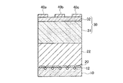
本発明の実施の形態に係る窒化物系化合物半導体素子の第1実施例は、図2に示すように、前述のGaとのメルトバックエッチングによって穴12が形成されており、Siからなる支持基板10と、第1の窒化物系化合物半導体として例えばAlNで形成されており、支持基板10の穴に蓋を閉じるように支持基板10上に設けられた第1の層22aと、第2の窒化物系化合物半導体として例えばGaNからなり、第1の層22aの上に形成されている第2の層22bと、更にその上に第1の層22aと第2の層22bとが繰り返し形成されて支持基板10上に設けられたバッファ層22と、第2の窒化物系化合物半導体として例えばGaNからなり、バッファ層22上に設けられたチャネル層31と、チャネル層31上に設けられており、チャネル層31よりもバンドギャップエネルギーが広く、チャネル層31との界面近傍に2次元電子ガス層を生じさせ、第3の窒化物系化合物半導体として例えばAlGaNからなる障壁層32と、障壁層32上に設けられたソース電極40a、ゲート電極40b、ドレイン電極40cとを備えるヘテロ接合電界効果トランジスタ(HFET)である。ここで、特許請求の範囲における素子形成領域30は、チャネル層31及び障壁層32に相当する。
(First embodiment)
As shown in FIG. 2, in the first example of the nitride-based compound semiconductor device according to the embodiment of the present invention, the
本発明の実施の形態に係る窒化物系化合物半導体素子の製造方法によって形成された窒化物系化合物半導体素子によれば、支持基板10に穴12を形成することでバッファ層22及び素子形成領域30からなるエピタキシャル成長層に生じる反りやクラックを抑制し、応力緩和をすることができる。これにより、エピタキシャル成長層の厚く形成することができ、高品質なエピタキシャル成長基板を得ることができる。そして、高品質なエピタキシャル成長基板が得られることにより、ウェハの大口径化にも寄与する。そして、エピタキシャル成長層の厚く形成することによって、窒化物系化合物半導体素子の縦方向の耐圧を向上することができる。
According to the nitride compound semiconductor device formed by the method for manufacturing a nitride compound semiconductor device according to the embodiment of the present invention, the
また、エピタキシャル成長工程中に支持基板10に穴12を形成することにより、成膜(蒸着、スパッタ等)工程、フォトリソグラフィ工程、エッチング工程等を行う必要がないため、窒化物系化合物半導体素子の製造リードタイムを短縮させることができる。
In addition, since the
(第2実施例)
本発明の実施の形態に係る窒化物系化合物半導体素子の第2実施例は、図3に示すように、穴12が形成された支持基板10と、支持基板10上に設けられたバッファ層22と、バッファ層22上に設けられた第1半導体層34と、第1半導体層34上に設けられた活性層36と、活性層36上に設けられた第2半導体層38と、第2半導体層38と低抵抗(オーミック)接触し第2半導体層38上に設けられた第2電極44と、支持基板10と低抵抗(オーミック)接触し支持基板10上に形成された第1電極42を備える発光ダイオード(LED)である。ここで第1半導体層34は、p型ドーパントを添加した例えばGaNのP型クラッド層である。活性層36は、例えばノンドープの窒化インジウムガリウム(InGaN)である。第2半導体層38は、n型ドーパントを添加した例えばGaNのN型クラッド層である。図3に示すように、第2半導体層38と第2電極44との間に挟まれたコンタクト層50を設けても良いし、バッファ層22を短絡するように支持基板10から第1半導体層34に延伸するように第1電極42を設けても良い。ここで、特許請求の範囲における素子形成領域30は、第1半導体層34、活性層36及び第2半導体層38に相当する。
(Second embodiment)
As shown in FIG. 3, the second example of the nitride-based compound semiconductor device according to the embodiment of the present invention includes a
本発明の実施の形態に係る窒化物系化合物半導体素子の製造方法によって形成された窒化物系化合物半導体素子によれば、支持基板10に穴12を形成されていることでエピタキシャル成長基板の反りやクラックの抑制、応力緩和をすることができる。これにより、活性層の結晶欠陥をより低減することが可能になり、高品質で高輝度な窒化物系化合物半導体素子を得ることができる。そして、高品質なエピタキシャル成長基板が得られることにより、ウェハの大口径化にも寄与し、窒化物系化合物半導体素子の取り数を増加することができる。
According to the nitride-based compound semiconductor element formed by the method for manufacturing a nitride-based compound semiconductor element according to the embodiment of the present invention, the
また、エピタキシャル成長工程中に支持基板10に穴12を形成することにより、成膜(蒸着、スパッタ等)工程、フォトリソグラフィ工程、エッチング工程等を行う必要がないため、窒化物系化合物半導体素子は、製造リードタイムを短縮させることができる。
In addition, by forming the
また、Siからなる支持基板10は活性層36から出る光(波長が約470nmの光)を吸収する。ここで、AlNの屈折率が約1.98であり、空気の屈折率が1.0であり、Siからなる支持基板10の屈折率は約4.5である。本発明の第2の実施形態において、第1の層22aと支持基板10との間に穴12が設けられており、活性層36から出た光が、第1の層(AlN)22a/穴(空気)10の界面に達した場合と、第1の層(AlN)22a/支持基板(Si)10の界面に達した場合とにおいて、第1の層22a/穴12の方が第1の層22a/支持基板10の界面よりも反射が生じやすい。したがって、光が第1の層22aと穴12との界面で屈折して、窒化物系化合物半導体素子の外部に取り出しやすくなり、窒化物系化合物半導体素子の発光効率を高めることができる。
Further, the
(その他の実施の形態)
上記のように、本発明は実施の形態によって記載したが、この開示の一部をなす記述及び図面はこの発明を限定するものであると理解するべきではない。この開示から当業者には様々な代替実施の形態、実施例及び運用技術が明らかになるはずである。
(Other embodiments)
As described above, the present invention has been described according to the embodiment. However, it should not be understood that the description and drawings constituting a part of this disclosure limit the present invention. From this disclosure, various alternative embodiments, examples and operational techniques should be apparent to those skilled in the art.
例えば、実施例において、ヘテロ接合電界効果トランジスタと半導体発光素子において示したが、ヘテロ接合を有する窒化物系化合物半導体からなる素子形成領域30の上にショットキーダイオードが形成された構造やMESFETに本発明の実施の形態を適応しても良い。
For example, in the embodiments, the heterojunction field effect transistor and the semiconductor light emitting device are shown. However, the present invention is not limited to a structure in which a Schottky diode is formed on the
このように、本発明はここでは記載していない様々な実施の形態等を包含するということを理解すべきである。したがって、本発明はこの開示から妥当な特許請求の範囲の発明特定事項によってのみ限定されるものである。 Thus, it should be understood that the present invention includes various embodiments and the like not described herein. Therefore, the present invention is limited only by the invention specifying matters in the scope of claims reasonable from this disclosure.
10…支持基板
12…穴
20…バッファ層成長核
22…バッファ層
22a…第1の層
22b…第2の層
30…素子形成領域
31…チャネル層
32…障壁層
34…第1半導体層
36…活性層
38…第2半導体層
40a…ソース電極
40b…ゲート電極
40c…ドレイン電極
42…第1電極
44…第2電極
50…コンタクト層
DESCRIPTION OF
Claims (4)
前記第1の層が形成された前記支持基板上にガリウムを含む第2の窒化物系化合物半導体からなる層を気相エピタキシャル成長させる工程
とを含むことを特徴とするエピタキシャル成長基板の製造方法。 A first nitride-based compound semiconductor made of a first nitride-based compound semiconductor which has a hole closed by a melt-back etching and a space closed by the hole on the upper surface of a silicon substrate which reacts with gallium to form a hole in the surface and does not contain gallium. Forming a layer of
Vapor phase epitaxial growth of a layer made of a second nitride compound semiconductor containing gallium on the support substrate on which the first layer is formed.
前記支持基板上に、不均一な厚みを有し且つ第1の窒化物系化合物半導体からなるバッファ層成長核を配置する工程と、
前記バッファ層成長核が配置された前記支持基板にガリウムを含む気相を供給する工程
とを含むことを特徴とする請求項1に記載のエピタキシャル成長基板の製造方法。 Forming the hole and the first layer comprises:
Disposing a buffer layer growth nucleus having a non-uniform thickness and comprising a first nitride-based compound semiconductor on the support substrate;
The method for producing an epitaxial growth substrate according to claim 1, further comprising: supplying a gas phase containing gallium to the support substrate on which the buffer layer growth nuclei are arranged.
前記第1の層が形成された前記支持基板上にガリウムを含む窒化物系化合物半導体からなる第2の層を気相エピタキシャル成長させる工程と、
前記第2の層を介して前記支持基板上に窒化物系化合物半導体からなる素子形成領域を形成する工程
とを含むことを特徴とする窒化物系化合物半導体素子の製造方法。 A first nitride-based compound semiconductor comprising a hole formed by melt-back etching on a top surface of a silicon substrate that reacts with gallium to form a hole in the surface and a space in which the hole is closed and does not contain gallium. Forming a layer of
Vapor phase epitaxially growing a second layer made of a nitride compound semiconductor containing gallium on the support substrate on which the first layer is formed;
Forming a device forming region made of a nitride compound semiconductor on the support substrate through the second layer. A method for manufacturing a nitride compound semiconductor device, comprising:
Priority Applications (1)
| Application Number | Priority Date | Filing Date | Title |
|---|---|---|---|
| JP2007268305A JP5163045B2 (en) | 2007-10-15 | 2007-10-15 | Epitaxial growth substrate manufacturing method and nitride compound semiconductor device manufacturing method |
Applications Claiming Priority (1)
| Application Number | Priority Date | Filing Date | Title |
|---|---|---|---|
| JP2007268305A JP5163045B2 (en) | 2007-10-15 | 2007-10-15 | Epitaxial growth substrate manufacturing method and nitride compound semiconductor device manufacturing method |
Publications (3)
| Publication Number | Publication Date |
|---|---|
| JP2009096655A JP2009096655A (en) | 2009-05-07 |
| JP2009096655A5 JP2009096655A5 (en) | 2010-12-02 |
| JP5163045B2 true JP5163045B2 (en) | 2013-03-13 |
Family
ID=40700005
Family Applications (1)
| Application Number | Title | Priority Date | Filing Date |
|---|---|---|---|
| JP2007268305A Expired - Fee Related JP5163045B2 (en) | 2007-10-15 | 2007-10-15 | Epitaxial growth substrate manufacturing method and nitride compound semiconductor device manufacturing method |
Country Status (1)
| Country | Link |
|---|---|
| JP (1) | JP5163045B2 (en) |
Cited By (1)
| Publication number | Priority date | Publication date | Assignee | Title |
|---|---|---|---|---|
| CN105931948A (en) * | 2011-08-18 | 2016-09-07 | 富士通株式会社 | Compound Semiconductor Device And Method For Manufacturing The Same |
Families Citing this family (11)
| Publication number | Priority date | Publication date | Assignee | Title |
|---|---|---|---|---|
| JP4996448B2 (en) * | 2007-12-25 | 2012-08-08 | パナソニック株式会社 | Method for creating a semiconductor substrate |
| JP5491116B2 (en) * | 2009-09-25 | 2014-05-14 | 日本碍子株式会社 | Epitaxial substrate for semiconductor element, semiconductor element, and manufacturing method of epitaxial substrate for semiconductor element |
| JP6284290B2 (en) | 2010-02-19 | 2018-02-28 | 三星電子株式会社Samsung Electronics Co.,Ltd. | Nitride semiconductor layer growth method and nitride semiconductor substrate formed thereby |
| JP5059205B2 (en) | 2011-03-03 | 2012-10-24 | 株式会社東芝 | Wafer and crystal growth method |
| KR101773091B1 (en) * | 2011-05-20 | 2017-08-30 | 엘지이노텍 주식회사 | A light emitting device and a method of fabricating the same |
| JP6185398B2 (en) * | 2014-01-31 | 2017-08-23 | 東京エレクトロン株式会社 | Gallium nitride crystal growth method and heat treatment apparatus |
| JP6556664B2 (en) * | 2015-07-08 | 2019-08-07 | クアーズテック株式会社 | Nitride semiconductor substrate |
| JP6288187B2 (en) * | 2016-08-22 | 2018-03-07 | 富士通株式会社 | Compound semiconductor device and manufacturing method thereof |
| US11515408B2 (en) * | 2020-03-02 | 2022-11-29 | Taiwan Semiconductor Manufacturing Company, Ltd. | Rough buffer layer for group III-V devices on silicon |
| KR102591149B1 (en) * | 2021-12-20 | 2023-10-19 | 웨이브로드 주식회사 | Method of manufacturing a non emitting iii-nitride semiconductor stacked structure |
| CN113540295B (en) * | 2021-06-23 | 2023-07-21 | 山西中科潞安紫外光电科技有限公司 | Manufacturing method of aluminum nitride substrate template |
Family Cites Families (3)
| Publication number | Priority date | Publication date | Assignee | Title |
|---|---|---|---|---|
| US5393993A (en) * | 1993-12-13 | 1995-02-28 | Cree Research, Inc. | Buffer structure between silicon carbide and gallium nitride and resulting semiconductor devices |
| JP2001122693A (en) * | 1999-10-22 | 2001-05-08 | Nec Corp | Ground substrate for crystal growth and method of producing substrate using the same |
| JP2007246289A (en) * | 2004-03-11 | 2007-09-27 | Nec Corp | Method for manufacturing gallium nitride semiconductor substrate |
-
2007
- 2007-10-15 JP JP2007268305A patent/JP5163045B2/en not_active Expired - Fee Related
Cited By (1)
| Publication number | Priority date | Publication date | Assignee | Title |
|---|---|---|---|---|
| CN105931948A (en) * | 2011-08-18 | 2016-09-07 | 富士通株式会社 | Compound Semiconductor Device And Method For Manufacturing The Same |
Also Published As
| Publication number | Publication date |
|---|---|
| JP2009096655A (en) | 2009-05-07 |
Similar Documents
| Publication | Publication Date | Title |
|---|---|---|
| JP5163045B2 (en) | Epitaxial growth substrate manufacturing method and nitride compound semiconductor device manufacturing method | |
| JP5554826B2 (en) | Epitaxial substrate and epitaxial substrate manufacturing method | |
| JP5552923B2 (en) | Semiconductor device and manufacturing method thereof | |
| US8803189B2 (en) | III-V compound semiconductor epitaxy using lateral overgrowth | |
| US8772831B2 (en) | III-nitride growth method on silicon substrate | |
| JP4332720B2 (en) | Method for manufacturing plate-like substrate for forming semiconductor element | |
| US20130140525A1 (en) | Gallium nitride growth method on silicon substrate | |
| JP6130995B2 (en) | Epitaxial substrate and semiconductor device | |
| JP5668339B2 (en) | Manufacturing method of semiconductor device | |
| JP2010232293A (en) | Semiconductor device | |
| JP2005217049A (en) | Semiconductor device | |
| JP2006100501A (en) | Plate type substrate for using to form semiconductor element and its manufacturing method | |
| US8643059B2 (en) | Substrate structure and method of manufacturing the same | |
| JP2016171196A (en) | Semiconductor device manufacturing method | |
| JP5412093B2 (en) | Semiconductor wafer manufacturing method and semiconductor device manufacturing method | |
| KR20190078654A (en) | Nitride semiconductor substrate, method of manufacturing the same, and semiconductor device | |
| JP2013239474A (en) | Epitaxial substrate, semiconductor device, and method of manufacturing semiconductor device | |
| JP4725763B2 (en) | Method for manufacturing plate-like substrate for forming semiconductor element | |
| US8541771B2 (en) | Semiconductor device and method of manufacturing the same | |
| KR20150000753A (en) | Nitride semiconductor and method thereof | |
| US8247794B2 (en) | Nitride semiconductor device | |
| JP2015070252A (en) | Semiconductor device, manufacturing method for semiconductor device, and wafer | |
| KR20150012119A (en) | Nitride semiconductor and method thereof | |
| JP2016058539A (en) | Method of manufacturing high electron mobility transistor | |
| US20190157500A1 (en) | Stripped method for prepairing semiconductor structure |
Legal Events
| Date | Code | Title | Description |
|---|---|---|---|
| A621 | Written request for application examination |
Free format text: JAPANESE INTERMEDIATE CODE: A621 Effective date: 20100915 |
|
| A521 | Written amendment |
Free format text: JAPANESE INTERMEDIATE CODE: A523 Effective date: 20100917 |
|
| A521 | Written amendment |
Free format text: JAPANESE INTERMEDIATE CODE: A523 Effective date: 20101014 |
|
| A977 | Report on retrieval |
Free format text: JAPANESE INTERMEDIATE CODE: A971007 Effective date: 20111117 |
|
| A131 | Notification of reasons for refusal |
Free format text: JAPANESE INTERMEDIATE CODE: A131 Effective date: 20111122 |
|
| A521 | Written amendment |
Free format text: JAPANESE INTERMEDIATE CODE: A523 Effective date: 20120120 |
|
| A131 | Notification of reasons for refusal |
Free format text: JAPANESE INTERMEDIATE CODE: A131 Effective date: 20120522 |
|
| A521 | Written amendment |
Free format text: JAPANESE INTERMEDIATE CODE: A523 Effective date: 20120717 |
|
| TRDD | Decision of grant or rejection written | ||
| A01 | Written decision to grant a patent or to grant a registration (utility model) |
Free format text: JAPANESE INTERMEDIATE CODE: A01 Effective date: 20121120 |
|
| A61 | First payment of annual fees (during grant procedure) |
Free format text: JAPANESE INTERMEDIATE CODE: A61 Effective date: 20121203 |
|
| FPAY | Renewal fee payment (event date is renewal date of database) |
Free format text: PAYMENT UNTIL: 20151228 Year of fee payment: 3 |
|
| R150 | Certificate of patent or registration of utility model |
Ref document number: 5163045 Country of ref document: JP Free format text: JAPANESE INTERMEDIATE CODE: R150 Free format text: JAPANESE INTERMEDIATE CODE: R150 |
|
| R250 | Receipt of annual fees |
Free format text: JAPANESE INTERMEDIATE CODE: R250 |
|
| R250 | Receipt of annual fees |
Free format text: JAPANESE INTERMEDIATE CODE: R250 |
|
| R250 | Receipt of annual fees |
Free format text: JAPANESE INTERMEDIATE CODE: R250 |
|
| LAPS | Cancellation because of no payment of annual fees |