JP5160776B2 - Photon detection method for detecting photons emitted from a channel and apparatus for supplying light to the channel - Google Patents
Photon detection method for detecting photons emitted from a channel and apparatus for supplying light to the channel Download PDFInfo
- Publication number
- JP5160776B2 JP5160776B2 JP2006339568A JP2006339568A JP5160776B2 JP 5160776 B2 JP5160776 B2 JP 5160776B2 JP 2006339568 A JP2006339568 A JP 2006339568A JP 2006339568 A JP2006339568 A JP 2006339568A JP 5160776 B2 JP5160776 B2 JP 5160776B2
- Authority
- JP
- Japan
- Prior art keywords
- channel
- light
- fluid
- longitudinal direction
- partition member
- Prior art date
- Legal status (The legal status is an assumption and is not a legal conclusion. Google has not performed a legal analysis and makes no representation as to the accuracy of the status listed.)
- Expired - Fee Related
Links
Images


Classifications
-
- G—PHYSICS
- G01—MEASURING; TESTING
- G01N—INVESTIGATING OR ANALYSING MATERIALS BY DETERMINING THEIR CHEMICAL OR PHYSICAL PROPERTIES
- G01N21/00—Investigating or analysing materials by the use of optical means, i.e. using sub-millimetre waves, infrared, visible or ultraviolet light
- G01N21/01—Arrangements or apparatus for facilitating the optical investigation
- G01N21/03—Cuvette constructions
- G01N21/05—Flow-through cuvettes
-
- B—PERFORMING OPERATIONS; TRANSPORTING
- B01—PHYSICAL OR CHEMICAL PROCESSES OR APPARATUS IN GENERAL
- B01L—CHEMICAL OR PHYSICAL LABORATORY APPARATUS FOR GENERAL USE
- B01L3/00—Containers or dishes for laboratory use, e.g. laboratory glassware; Droppers
- B01L3/50—Containers for the purpose of retaining a material to be analysed, e.g. test tubes
- B01L3/502—Containers for the purpose of retaining a material to be analysed, e.g. test tubes with fluid transport, e.g. in multi-compartment structures
- B01L3/5027—Containers for the purpose of retaining a material to be analysed, e.g. test tubes with fluid transport, e.g. in multi-compartment structures by integrated microfluidic structures, i.e. dimensions of channels and chambers are such that surface tension forces are important, e.g. lab-on-a-chip
- B01L3/502715—Containers for the purpose of retaining a material to be analysed, e.g. test tubes with fluid transport, e.g. in multi-compartment structures by integrated microfluidic structures, i.e. dimensions of channels and chambers are such that surface tension forces are important, e.g. lab-on-a-chip characterised by interfacing components, e.g. fluidic, electrical, optical or mechanical interfaces
-
- G—PHYSICS
- G01—MEASURING; TESTING
- G01N—INVESTIGATING OR ANALYSING MATERIALS BY DETERMINING THEIR CHEMICAL OR PHYSICAL PROPERTIES
- G01N21/00—Investigating or analysing materials by the use of optical means, i.e. using sub-millimetre waves, infrared, visible or ultraviolet light
- G01N21/01—Arrangements or apparatus for facilitating the optical investigation
- G01N21/03—Cuvette constructions
- G01N21/0303—Optical path conditioning in cuvettes, e.g. windows; adapted optical elements or systems; path modifying or adjustment
-
- B—PERFORMING OPERATIONS; TRANSPORTING
- B01—PHYSICAL OR CHEMICAL PROCESSES OR APPARATUS IN GENERAL
- B01L—CHEMICAL OR PHYSICAL LABORATORY APPARATUS FOR GENERAL USE
- B01L2300/00—Additional constructional details
- B01L2300/06—Auxiliary integrated devices, integrated components
- B01L2300/0627—Sensor or part of a sensor is integrated
- B01L2300/0654—Lenses; Optical fibres
-
- B—PERFORMING OPERATIONS; TRANSPORTING
- B01—PHYSICAL OR CHEMICAL PROCESSES OR APPARATUS IN GENERAL
- B01L—CHEMICAL OR PHYSICAL LABORATORY APPARATUS FOR GENERAL USE
- B01L2300/00—Additional constructional details
- B01L2300/08—Geometry, shape and general structure
- B01L2300/0809—Geometry, shape and general structure rectangular shaped
- B01L2300/0816—Cards, e.g. flat sample carriers usually with flow in two horizontal directions
-
- B—PERFORMING OPERATIONS; TRANSPORTING
- B01—PHYSICAL OR CHEMICAL PROCESSES OR APPARATUS IN GENERAL
- B01L—CHEMICAL OR PHYSICAL LABORATORY APPARATUS FOR GENERAL USE
- B01L2300/00—Additional constructional details
- B01L2300/16—Surface properties and coatings
- B01L2300/168—Specific optical properties, e.g. reflective coatings
-
- G—PHYSICS
- G01—MEASURING; TESTING
- G01N—INVESTIGATING OR ANALYSING MATERIALS BY DETERMINING THEIR CHEMICAL OR PHYSICAL PROPERTIES
- G01N21/00—Investigating or analysing materials by the use of optical means, i.e. using sub-millimetre waves, infrared, visible or ultraviolet light
- G01N21/01—Arrangements or apparatus for facilitating the optical investigation
- G01N21/03—Cuvette constructions
- G01N2021/0346—Capillary cells; Microcells
-
- G—PHYSICS
- G01—MEASURING; TESTING
- G01N—INVESTIGATING OR ANALYSING MATERIALS BY DETERMINING THEIR CHEMICAL OR PHYSICAL PROPERTIES
- G01N21/00—Investigating or analysing materials by the use of optical means, i.e. using sub-millimetre waves, infrared, visible or ultraviolet light
- G01N21/62—Systems in which the material investigated is excited whereby it emits light or causes a change in wavelength of the incident light
- G01N21/63—Systems in which the material investigated is excited whereby it emits light or causes a change in wavelength of the incident light optically excited
- G01N21/64—Fluorescence; Phosphorescence
-
- G—PHYSICS
- G01—MEASURING; TESTING
- G01N—INVESTIGATING OR ANALYSING MATERIALS BY DETERMINING THEIR CHEMICAL OR PHYSICAL PROPERTIES
- G01N21/00—Investigating or analysing materials by the use of optical means, i.e. using sub-millimetre waves, infrared, visible or ultraviolet light
- G01N21/62—Systems in which the material investigated is excited whereby it emits light or causes a change in wavelength of the incident light
- G01N21/63—Systems in which the material investigated is excited whereby it emits light or causes a change in wavelength of the incident light optically excited
- G01N21/65—Raman scattering
Abstract
Description
本発明は、流体用構造物内に形成されたチャネルから放出される光子を検知する光子検知方法又はそのチャネルに光を供給する技術に関する。 The present invention relates to a photon detection method for detecting photons emitted from a channel formed in a fluid structure or a technique for supplying light to the channel .
非特許文献1には、高屈折率物質による高反射率面で囲まれた低屈折率媒体内、例えばファブリペロー共振子の表面にある高反射率面等に囲まれた水溶液内に、光を閉じこめる技術が記載されている。
既存技術例えば上述の従来技術を利用し光を伝搬させる際、検体を含む物体をどのようにすれば効率的且つ実効的に照明できるかが、大きな問題となることがある。例えば、大きな面積を対象に励起光を照射する場合である。即ち、互いの位置が大きく離れている多数の物体を同時に照明し、伝搬してくる照明光に応じそれらの物体から放出される光子を検知しなければならない状況にて、際立った問題となる。 When light is propagated using the existing technology, for example, the above-described conventional technology, how to efficiently and effectively illuminate an object including a specimen may be a big problem. For example, it is a case where a large area is irradiated with excitation light. That is, it becomes a prominent problem in a situation where a large number of objects whose positions are greatly separated from each other must be illuminated at the same time, and photons emitted from these objects must be detected in response to propagating illumination light.
こうした問題は、例えば光を用いて検体を調べるバイオセンサにて発生する。そうしたセンサによって検体を調べる際にはその光と検体とを相互作用させる必要があるが、通常、そうした相互作用は非常に弱いものである。そのため相互作用を強化することが求められており、その手段としては、検体を含有する流体その他の物質それ自体を光伝搬媒体として光導波路を構成する、という手法が期待されている。しかしながら、実際には、当該流体はその周囲にある物質より低屈折率であり、従ってその流体内に光を閉じこめられないのが普通である。そのため、従来は、光導波路を用いるとしても、その光導波路の周縁に沿った方向からエバネッセント波により弱い相互作用を標的分子との間に引き起こす、という使用形態に留まっていた。 Such a problem occurs, for example, in a biosensor that examines a specimen using light. When examining a specimen with such a sensor, it is necessary to cause the light to interact with the specimen, but such interaction is usually very weak. Therefore, it is required to enhance the interaction, and as a means for that, a method of constructing an optical waveguide using a fluid or other substance itself containing a specimen as a light propagation medium is expected. In practice, however, the fluid has a lower refractive index than the surrounding material, and therefore it is usually not possible to confine light within the fluid. For this reason, conventionally, even if an optical waveguide is used, it has remained in a usage form in which a weak interaction is caused between a target molecule and an evanescent wave from a direction along the periphery of the optical waveguide.
従って、チャネル又はその構成部分に光を供給する技術を改良し、上掲の問題群を解決することが、求められているといえよう。 Therefore, it can be said that there is a need to improve the technology for supplying light to the channel or its constituent parts and to solve the above problems.
ここに、本発明の一実施形態に係る光子検知方法は、流体用構造物内に形成されたチャネルから放出される光子を検知する光子検知方法であって、前記チャネルは長手方向に伸び、長さに沿った何れの位置においても各断面を有し、各位置の断面において、前記チャネルの境界は、前記チャネル内の流体よりも高い屈折率を有する物質によってほぼ全体的に囲われ、前記流体用構造物は前記チャネルに仕切部材を含み、前記仕切部材は光透過性部を含み、前記流体用構造物は、前記チャネルの境界に少なくとも部分的に沿った前記長手方向に、前記仕切部材を越えて前記チャネルの突出部へ伸びる光透過性部材をさらに含み、前記光子検知方法は、前記流路内に流体がある状態で、前記長さの一部に沿った断面において、伝搬する光のうち断面内強度比で約10%以上(例えば約90%)の部分が前記流体内を伝搬することとなるように前記流路を通して前記長手方向に光を伝搬させるステップであって、前記仕切部材を越えた前記光透過性部材と、前記チャネルの前記突出部と、前記仕切部材の前記光透過性部とを通して、前記チャネルの外部にある光源から光を供給するステップを含み、前記光源からの前記光は前記長手方向に対して斜めの方向から前記チャネルに入る、前記光を伝搬させるステップと、前記伝搬する光に応じて前記チャネルから放出される光子を検知するステップと、を含む。 Here, engagement Ru photon detection method according to an embodiment of the present invention is a photon detection method for detecting photons emitted from the channel formed in the fluid structure, said channel extends in the longitudinal direction Each channel has a cross-section at any location along the length, and in each location cross-section, the boundary of the channel is substantially entirely surrounded by a material having a higher refractive index than the fluid in the channel; The fluid structure includes a partition member in the channel, the partition member includes a light transmissive portion, and the fluid structure includes the partition in the longitudinal direction at least partially along a boundary of the channel. A light transmissive member extending beyond the member to the protruding portion of the channel, wherein the photon detection method propagates in a cross section along a portion of the length with fluid in the flow path Out of light A portion of about 10% or more at an internal intensity ratios (e.g., about 90%) the step of propagating light in the longitudinal Direction through the channel so as to be propagated through the fluid, said partition member Supplying light from a light source external to the channel through the light transmissive member beyond, the protrusion of the channel, and the light transmissive portion of the partition member, light entering the channel from a direction oblique to the longitudinal direction, comprising the steps of: propagating the light, and a step of detection knowledge photons emitted from said channel in response to the propagating light.
また、本発明の一実施形態に係るチャネルに光を供給する装置は、流体用構造物と、前記流体用構造物内に形成され、流体を含むことが可能なチャネルであって、前記チャネルは長手方向に伸び、長さに沿った何れの位置においても各断面を有し、各位置の断面において、前記チャネルの境界は、前記チャネル内の流体よりも高い屈折率を有する物質によってほぼ全体的に囲われる前記チャネルと、前記流体用構造物の前記チャネルにある仕切部材であって、光透過性部を含む前記仕切部材と、前記流体用構造物に含まれる光透過性部材であって、前記チャネルの境界に少なくとも部分的に沿った前記長手方向に、前記仕切部材を越えて前記チャネルの突出部へ伸びる光透過性部材と、前記長手方向に前記チャネルを通って伝搬する光を供給する照明手段であって、前記長さの一部に沿った断面において、伝搬する光のうち断面内強度比で約10%以上(例えば約90%)の部分が前記流体内を伝搬することとなるように、前記照明手段は前記チャネルの外部から光を供給する光源を含み、前記光源は前記仕切部材を越えた前記光透過性部材と、前記チャネルの前記突出部と、前記仕切部材の前記光透過性部とを通して光を供給し、前記光源からの前記光は前記長手方向に対して斜めの方向から前記チャネルに入る前記照明手段と、を含む。 An apparatus for supplying light to a channel according to an embodiment of the present invention includes a fluid structure and a channel formed in the fluid structure and capable of containing a fluid, Extending in the longitudinal direction and having each cross section at any position along the length, in each position cross section, the boundary of the channel is substantially entirely defined by a material having a higher refractive index than the fluid in the channel. A partition member in the channel of the fluid structure, the partition member including a light transmissive portion, and a light transmissive member included in the fluid structure, A light transmissive member extending in a longitudinal direction at least partially along a boundary of the channel and extending beyond the partition member to a protruding portion of the channel and a light propagating through the channel in the longitudinal direction; A lighting unit that, in a cross section along a portion of said length, and that the portion of about 10% or more in cross-section in the intensity ratio of the propagating light (e.g. about 90%) is propagated through the fluid composed manner, the illumination means comprises a light source for supplying light from the outside of the channel, the light source and the light transmitting member beyond the partition member, and the protruding portion of the channel, the said partition member The illumination means supplies light through a light transmissive portion, and the light from the light source enters the channel from a direction oblique to the longitudinal direction.
図1に、支持基体たる流路付構造物12上に形成されたアナライザ10について、その構成要素のうち幾つかを模式的に示す。図示の如く、この流路付構造物12には蛇のように曲がりくねったチャネル14が形成されている。また、このチャネル14は、その内部に物体16を通すことができるよう、形成されている。物体16は、例えば、解析対象となる検体を含有する小体積流体乃至液滴であり、適当な物質例えば流体によって、このチャネル14内を運ばれていく。
FIG. 1 schematically shows some of the components of the
以下説明する構成にて検査しうる物体16には、例えば、液滴、流体の微小体積部分、単独の分子、凝集した分子、分子クラスタ、細胞、ウイルス、バクテリア、タンパク質、DNA(デオキシリボ核酸)、マイクロパーティクル、ナノパーティクル、エマルジョン等と称されるものが含まれる。液滴や流体微小体積部分の中には、例えば原子や分子等のように、自発的に又は励起輻射(以下励起光とも称する)に応じ発光する粒子や、入射光を吸収する粒子や、入射光を散乱させる粒子等が含まれる。それらのうち励起光に応じ蛍光を発する粒子のことをその液滴等の蛍光成分と呼び、特定光子エネルギ(光子が有するエネルギ即ち波長又は周波数のこと)の入射光を吸収するためその光子エネルギでは反射や散乱が生じない粒子のことをその液滴等の吸収成分と呼び、特定光子エネルギの入射光を散乱させる粒子のことをその液滴等の散乱成分と呼ぶ。即ち、液滴内の検体即ち調査対象化学種は、蛍光成分、吸収成分、散乱成分等として振る舞う。
Examples of the
物体16は、図中矢印線20で示されるように、主流体により搬送されてチャネル14内に入っていく。その送給元は例えば補給用リザーバ及び標本ウェルであり、主流体内への入り方は等速送出用電極22によって制御される。ここでは等速送出(metering)の方法として電極22による電気的等速送出を使用しているが、圧力による等速送出も採用可能である。更に、チャネル14内に液滴その他の小物体を供給するのに使用できる手法は他にもある。
The
アナライザ10に設けるチャネルの本数は適宜定めることができる。その場合、各チャネルの構成は図1中のチャネル14と同様の構成でよい。各チャネルに対する検体標本の供給元例えば標本ウェル、リザーバ、コンテナ等は、チャネル毎に設けてもよいし複数個のチャネルで共用してもよい。更に、各チャネルに設ける部材の個数及び種類は、そのチャネルを用いどのような種類の解析を実施したいかに応じて設定するとよく、従ってそれらはチャネル毎に異なる個数又は種類となりうる。また、1個の広いチャネルを区画して複数本のチャネルを形成すること、例えば互いに平行な数本のチャネルを形成することも可能である。
The number of channels provided in the
物体16を搬送するための流体は、矢印線24で示すように別の入口からチャネル14内に入れることもできる。矢印線20又は24に沿ってチャネル14内に入った流体が辿る経路は、様々な装置により制御される。例えば、この図のチャネル14に設けられている分岐ジャンクションのうち2個は、それぞれ別のアウトレットにつながっており且つ弁を有している。図中の弁30及び32がそれである。チャネル14内の流体は、矢印線26で示すように弁30に対するトグル制御によって一方のアウトレットから排出させることができ、また、矢印線28で示すように弁32に対するトグル制御によって他方のアウトレットからも排出させることができる。即ち、物体16が到来したとき弁30又は32を開かせることによって、物体16及びそれを搬送する流体を、その弁に対応するアウトレットから排出させることができる。これは物体16を対象とするゲーティングの一形態であり、他の形態によるゲーティングも実施可能である。帯電している粒子であればクーロン力によって偏向させることができるし、分極可能な粒子であれば誘電泳動力によって偏向させることができる。そして、流体は、矢印線34で示すように、最後段に設けられたアウトレットを介しチャネル14から排出させることができる。
Fluid for conveying the
流体の流れを維持するには、チャネル14の長手方向に沿って、流体の流れを推進する部材を設ければよい。この推進部材は従来からある種類のものでよく、図示の例では電気浸透ポンプ40が用いられている。推進部材には、流体の流れを維持する機能だけでなく、圧送法によりシステムを洗浄する機能や同じく圧送法により流体を初期充填する機能を担わせることができる。電気浸透ポンプ40を含め、流路付構造物12に設けられた各種部材は、相応の回路を設けることによって、相互に同期をとりつつ動作させることができる。
In order to maintain the fluid flow, a member for propelling the fluid flow may be provided along the longitudinal direction of the
チャネル14は、180度に曲がった屈曲部により複数個の直線部間をつないだ構成を有している。チャネル14沿いには、それぞれ対応する直線部内を移動していく物体16についての情報を取得するため、複数個の検知部材が次から次へと配されている。そのうちコールタカウンタ(Coulter counter)50は電気式粒子サイズ検知器であり、ミー散乱センサ(Mie scatter sensor)52は光学式検知器である。ミー散乱センサ52は、側方からチャネル14に入射しチャネル14内の物体16例えば粒子により散乱された光を検知する。
The
チャネル14沿いには、上述の一群の検知部材として、更に、可視光や赤外光に反応する光吸収検知部材54、第1の蛍光検知部材56、第2の蛍光検知部材58、並びにラマン散乱検知部材60が配されている。更に、特性的に所定条件を満たす検体がチャネル14沿いのある位置を通過したとき、そのこと又はその時刻を示す起動信号を出力する光学式又は電気式の起動部品を、検知部材の一種として設けてもよい。こうした起動部品は既存の技術で実現できる。更に、生体粒子サイズ検知用差動抵抗に代え、電子病理学向けEIS(electrical impedance spectroscopy)用検知部材を、設けることもできる。
Along the
図1に示す一群の検知部材によれば、移動する粒子その他の物体16についてのスペクトラム情報を取得することができる。取得したスペクトラム情報を用いれば、直交性のあるかたちで物体16の特徴を調べることができ、また物体16の識別を信頼性よく行うことができる。直交性のあるかたちで、とは、例えば相異なる光子エネルギレンジでの光子検知により得られた複数種類の情報や、相異なる強度レンジでの光子検知により得られた複数種類の情報のように、その間に直交性が成り立つ複数種類の情報を利用して、という意味である。素材選択が適切であれば、深紫外域から遠赤外域更にはTHz帯の周波数に至る光子エネルギレンジにてくまなく、スペクトラム情報を取得可能である。
According to the group of detection members shown in FIG. 1, spectrum information about moving particles and
また、アナライザ10は、多信号解析を実行可能な構成、従って生体物質(bioagent)を試薬なしで識別可能な構成とすることができる。
In addition, the
検知部材54、56、58及び60はそれぞれIC64、66、68又は70を有しており、それらIC64、66、68及び70はそれぞれフォトセンサアレイを内蔵しており、各フォトセンサアレイは一群のセルから構成されており、各セル群はある光子エネルギレンジ内の光子を検知するよう構成されている。言い換えれば、検知部材54、56、58及び60は内蔵するセル群により実現されている。更に、IC64、66、68及び70にて光子を検知可能な光子エネルギレンジを互いに同一にしてもよいし違えてもよい。例えば、IC66を構成するセル群は上述の如く可視域から紫外域に至る光子エネルギレンジにて光子を検知し、IC68を構成するセル群は同じ可視域から紫外域に至る光子エネルギレンジではあるがIC66を構成するセル群のそれとは異なる光子エネルギレンジにて光子を検知し、IC70を構成するセル群は赤外域に属する光子エネルギレンジにて光子を検知する、といった具合に構成することができる。また、検知可能な光子エネルギレンジが同一の複数のICでも、互いに異なる検知結果が得られるようも構成することができる。例えば、IC66及び68に係る光子エネルギレンジが互いに同一であるとする。そうした場合でも、それらIC66及び68に対応する励起光源同士を、互いに別々の波長で発光するように構成しておけば、互いに異なる結果が得られる。即ち、そうした構成では、一方の波長の励起光を受けて物体16が発する蛍光が例えばIC66で検知され、他方の波長の励起光を受けて物体16が発する蛍光が例えばIC68で検知されることとなるので、蛍光検知結果が両IC間で異なる結果となりうる。なお、励起光源は、LED(発光ダイオード)、レーザ等によって実現することができる。また、検知部材54、56、58及び60を構成するセル群の光子検知可能波長域即ち光子エネルギレンジは、この例では複数個のサブレンジに分割されており、各サブレンジに属する光子をセルの小群(組)のうち対応するものが検知する構成を採っている。各小群に係るサブレンジを他の小群のそれと同じにしてもかまわないが、同一フォトセンサアレイ内小群のうち少なくとも2個は、互いに異なるサブレンジにて光子を検知するよう構成しておく。
The
更に、検知部材56、58及び60には励起手段乃至照明手段を併設することができる。励起や照明の手法は、物体16から光を放射させることが可能な手法である限り、どのような手法でもよい。励起手段とは電磁波輻射又は試薬のことをいい、照明手段とは物体に光を供給してその物体から光子を放出させ又はその物体により光子を散乱させる手段のことをいう。照明手段は単独の光源から構成してもよいし複数個の光源を組み合わせて構成してもよい。
Further, the
また、単独の粒子又は低濃度の生物学的若しくは化学的物質の特性を調べることができるようアナライザ10を構成する場合には、とりわけ、光標的間相互作用の強化(enhanced light-target interaction)が重要となる。本実施形態では、光標的間相互作用強化のために反共振光導波構造(anti-resonant waveguide;文脈に応じ反共振光導波路とも記す)を採用している。一般に、反共振光導波路は、コア部をそれより高屈折率のクラッディング部で囲んだ構造を有する。本実施形態におけるチャネル14は、その内部にあり検体を含有する流体をコア部として形成された反共振光導波構造を採っている。従って、チャネル14内流体により光を導波し、チャネル14の長手方向に沿って、またかなり長い距離に亘り、フォトニック相互作用を発生させることができる。これによって、光標的間相互作用が強化される。また、この反共振光導波構造における光標的間相互作用強化を妨げないようにするため、ここでは更に、IC66、68及び70を複数個のスペーサ72によって支持する構造を採用している。このようにすれば、IC66、68及び70とチャネル14の対応部分との間に適正な幅の間隙が形成されるため、IC66、68及び70が反共振光導波構造と機械的に抵触、競合することを、防ぐことができる。
Also, when the
光学的バイオセンサにおいては、光と検体例えば標的分子の間の相互作用が非常に弱いのが一般的である。反共振光導波構造は、その長手方向に沿って光が伝搬し、従って長い距離に亘り相互作用が生じる構造であるため、光と検体との間の相互作用が格段に強くなる。また、こうした構造は、伝搬する光の波長の違いや当該構造を形成する膜の厚みの影響を受けにくいため多信号解析と非常に相性がよく、エバネッセント波を利用して励起を行う従来の光導波路利用センサ(そのためチャネルを非常に細くせざるを得なかったセンサ)と対照的なことに、チャネル断面寸法をかなり例えば数mm程にも拡げることができる。こうした反共振光導波構造は、例えば、ガラス毛細管内にエアロゾルを入れた構造や、或いはガラススライド間に液体膜を挟んだ構造によって、好適に実現できる。励起は相応の電磁波を照射することによって行うことができる。 In optical biosensors, the interaction between light and an analyte, such as a target molecule, is generally very weak. The anti-resonant optical waveguide structure is a structure in which light propagates along the longitudinal direction thereof, and thus interaction occurs over a long distance, and thus the interaction between the light and the specimen is remarkably strong. In addition, such a structure is not easily affected by the difference in the wavelength of propagating light or the thickness of the film forming the structure, so it is very compatible with multi-signal analysis, and is a conventional optical system that uses evanescent waves for excitation. In contrast to waveguide-based sensors (thus sensors that have had to be very narrow in channel), the channel cross-sectional dimensions can be increased considerably, for example by a few millimeters. Such an antiresonant optical waveguide structure can be suitably realized by, for example, a structure in which an aerosol is put in a glass capillary tube or a structure in which a liquid film is sandwiched between glass slides. Excitation can be performed by irradiating a corresponding electromagnetic wave.
光標的間相互作用強化用光導波構造例えば反共振光導波構造を採用する場合、背景励起光抑圧機構の付加が必要になるかもしれない。背景励起光抑圧機構としては、例えば波長炉波特性を有する部材を、チャネル14を形成する壁の一部又はフォトセンサアレイの頂部被覆の一部として設ければよい。
When an optical waveguide structure for enhancing interaction between optical targets, for example, an anti-resonant optical waveguide structure, is adopted, it may be necessary to add a background excitation light suppression mechanism. As the background excitation light suppression mechanism, for example, a member having a wavelength furnace wave characteristic may be provided as a part of the wall forming the
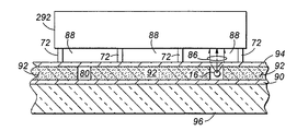
図2に、図1中の線2−2に沿ったアナライザ10の断面を模式的に示す。図示したのは第2の蛍光検知部材58を含む部分の断面であるが、第1の蛍光検知部材56も本質的にこれと同様の断面を呈する。また、ラマン散乱検知部材60の断面にも、これに類似する部分がある。
FIG. 2 schematically shows a cross section of the
矢印線82で示す如くチャネル14の構成部分80内を下流へと移動中の物体16は、例えばレーザ光源やLED光源として構成された光源84等の励起部材から、励起光を受光する。チャネル14内にカップリングしチャネル14内に反共振光導波を引き起こすことが可能な光子エネルギレンジは限られておらず、従って励起光としては様々な光子エネルギを有する輻射を使用できる。チャネル構成部分80は、光源84から発せられた光を受け反共振光導波路等として機能し、その内部で発生する光標的間相互作用を強化する。なお、蛍光性の分子を連続的に励起できる手法としては、こうした手法の他に、レーザビーム走査によって移動分子を追尾する、LEDリニアアレイを用い経路沿いで粒子を励起状態に保つ、粒子経路沿いに平行ビームを配する(導波は行わない)、ファブリペロー型又はこれに類似するタイプの(空胴)共振子を設けその共振子を通して粒子含有媒体に数回に亘り光を供給する、等の手法がある。
As indicated by the
反共振光導波モードを使用して輻射を検知する部材と、流路付構造物との組合せは、幾つかの点で特に有利である。それは、流体チャネルそれ自体を反共振光導波路として使用でき、しかもその流体チャネル(反共振光導波路)が様々な形態、構成を採りうるからである。採りうる形態、構成としては、毛細管内にエアロゾルを入れそのエアロゾルにより検体を搬送する、チャネル内又はガラススライド間に液体膜を形成しその液体膜内で検体を搬送する、といった形態がある。 The combination of a member that detects radiation using an anti-resonant optical waveguide mode and a structure with a flow path is particularly advantageous in several respects. This is because the fluid channel itself can be used as an anti-resonant optical waveguide, and the fluid channel (anti-resonant optical waveguide) can take various forms and configurations. Possible forms and configurations include a form in which an aerosol is placed in a capillary tube and a specimen is transported by the aerosol, a liquid film is formed in a channel or between glass slides, and the specimen is transported in the liquid film.
光源84からの光が到達すると、物体16に内包されている検体が蛍光、即ち光子エネルギスペクトラムに特徴のある光を放射する。放射された光の一部は光束86となり検知器アセンブリ87に向かう。検知器アセンブリ87は少なくともIC68を有しており、そのIC68上にはフォトセンサアレイがあるので、光束86内の光子はそのフォトセンサアレイを構成するセル群によって検知されることとなる。なお、検知器アセンブリ87は、IC68上のフォトセンサアレイがチャネル構成部分80内における物体16の移動経路近くに位置するよう且つ当該移動経路に対して平行になるよう、ひいては集光効率が高まるよう、配置しておく。
When light from the
図中の検知器アセンブリ87は、反共振光導波を邪魔しないよう複数個のスペーサ72によって支持されている。即ち、複数個のスペーサ72はチャネル構成部分80内に入り込まないように配置されており、それによって検知器アセンブリ87の下方には空隙88が生じているので、チャネル構成部分80内での反共振光導波は阻害されない。なお、ここでは空隙88を形成しているがこれは反共振光導波が阻害されることを防ぐ方法の一例に過ぎず、例えば真空層、気体層、液体層、液体膜等、低屈折率の構造を設けることも導波阻害防止に有益である。低屈折率の素材を使用する場合、形成乃至使用すべき間隙、層又は膜の幅若しくは厚みは数μm程度、例えば10μmという狭さ乃至薄さになる。
The
また、物体16はチャネル構成部分80内通過中は途切れなしに励起光を受光するので、物体16内の検体からの蛍光もフォトセンサアレイの長手方向に沿って途切れなく発生し続ける。従って、物体16がチャネル構成部分80内を移動する期間を途切れなく利用して、スペクトラム情報を収集することができる。
Since the
図2に示した構造は、更に、ラマン散乱検知部材60をかたちづくる構造としても用いることができる。ラマン散乱検知部材60をそのようにして形成した場合、出力信号は、完全なラマンスペクトラムではなく、それぞれ、ラマンスペクトラム間にある狭い間隙の幅なり、指定された複数本のラマンライン間の強度比なりを表す信号になる。
The structure shown in FIG. 2 can also be used as a structure that forms the Raman
図2に示した形態でラマン散乱検知部材60を実現するには、光源84及びIC70を所定の仕様に適合させることが必要となろう。加えて、光サンプリングを効率的且つ確実に行えるようにするため、IC70を構成するフォトセンサアレイとチャネル14との間に、相応の光学部品を配置することが必要となろう。
In order to realize the Raman
図2からは、更に流路付構造物12の構成も看取できる。即ち、図中の構成では、光透過性のガラス又はシリコン基板である支持層90の上に、ポリジメチルシロキサン(polydimethylsiloxane;PDMS)によりマイクロモールド層92が形成されており、更にこのマイクロモールド層92内にチャネル14が形成されている。図中の各層例えばマイクロモールド層92をパターニングする際には、検体と検体の間の干渉ができるだけ少なくなるよう、チャネル14のうちの光標的間相互作用発生部分の長さを設定しておくとよい。
From FIG. 2, the structure of the
PDMSからなるパターン化マイクロモールド層92を形成するには、例えば、ガラス等からなる支持層90の上にSU−8ポリマからなるテンプレートを形成し、その上にPDMSを堆積、成長させた上で、テンプレートを除去すればよい。そうすれば、テンプレートがなかった場所にパターン状の構造物が形成される。マイクロモールド層92の上を覆っている光透過構造物はガラス等により形成された光透過性プレート層94である。
In order to form the patterned
こうした方法に代え、ガラスをエッチングしチャネルを形成する、という手法も使用できる。また、SU−8等のポリマ素材の層をマイクロファブリケーション法によりパターニングしてチャネルを形成すれば、アスペクト比の高いチャネル壁を形成できる。また、チャネル14内で検体を搬送する媒体に応じ、チャネル14にまつわる各種パラメタを設定すれば、更に好適な結果が得られる。
Instead of such a method, a method of etching a glass to form a channel can also be used. Further, if a channel is formed by patterning a polymer material layer such as SU-8 by a microfabrication method, a channel wall having a high aspect ratio can be formed. Further, if various parameters related to the
例えば、チャネル14にまつわるパラメタのうち、チャネル壁の接着性(adhesiveness)即ち生体粒子、バクテリア、タンパク質等の吸引されやすさを左右するパラメタをうまく設定することが、特に効果的である。
For example, among the parameters related to the
チャネル壁面等の接着性による標本損失を減らす方法は幾つかある。具体的には、チャネル壁面等に抗接着性被覆を被着形成しておくことで、その壁面への生体粒子等の検体の付着を防止できる。特に、ポリエチレングリコール(polyethylene glycol;PEG)の浸漬被膜を形成しておけば、大抵の生物系素材はその被着を好適に防止することができ、それでいて水溶液に作用する毛細管力も確保することができる。この他の使用可能な被覆としては、例えばパリレンC(parylene C;商標)や、気相成長テトラグリム(tetraglyme;tetraethylene glycol dimethyl ether;pentaoxa pentadodecan)による被覆がある。どういった被覆を設けるかは、例えば標本の特性、素材界面の化学的性質、動作の条件・形態・機序等に応じて決めればよい。また、前述の反共振導波という手法はその内径が最大約1.0mmのチャネルに対して適用され、また恐らくはそれ以上の内径のチャネルに対しても適用可能な手法である。このように太いチャネルに適用される手法であるので、目詰まりのような大きな問題が壁面接着によって生じる恐れは少ないが、それでもなお接着防止措置は有益である。即ち、接着防止措置を施すことで、チャネル内壁への素材や物体の接着を防止でき、従って接着した素材や物体から光が放射され背景スプリアス光になってしまうことを防ぐことができる。 There are several ways to reduce specimen loss due to adhesion of channel walls and the like. Specifically, by attaching an anti-adhesive coating on the channel wall surface or the like, it is possible to prevent adhesion of a specimen such as biological particles to the wall surface. In particular, if a dip coating of polyethylene glycol (PEG) is formed, most biological materials can be suitably prevented from adhering, and capillary force acting on an aqueous solution can be secured. . Other usable coatings include, for example, coating with parylene C (trademark) and vapor-grown tetraglyme (tetraethylene glycol dimethyl ether). What kind of coating is provided may be determined in accordance with, for example, the characteristics of the specimen, the chemical properties of the material interface, the operating conditions / form / mechanism, and the like. The above-described anti-resonance waveguide method is applied to a channel having an inner diameter of about 1.0 mm at the maximum, and is probably applicable to a channel having an inner diameter larger than that. Since the technique is applied to such a thick channel, there is little possibility that a big problem such as clogging will be caused by the adhesion to the wall surface, but the adhesion prevention measure is still useful. That is, by applying an adhesion prevention measure, it is possible to prevent the material or object from adhering to the inner wall of the channel, and thus it is possible to prevent light from being emitted from the adhered material or object and becoming background spurious light.
更に、図2中、支持層90の表面のうちPDMSによるマイクロモールド層92と逆側の面上には、その一部表面が励起光結合部98として機能するよう光学部品96が設けられている。光源84から発せられた光は、この面98を通ることで、チャネル14の構成部分80内にある反共振光導波路にカップリング(結合)される。面98は良好な結合が実現されるように形成されている。また、適当な素材と適当なプロセスを用いさえすれば、支持層90及び光学部品96を同一の素材による単一の層として形成することもできる。
Further, in FIG. 2, an
図3に、検知器アセンブリ87の一例構成を模式的に示す。この図の検知器アセンブリ87内のIC68はフォトセンサアレイ100を有しており、更に当該IC68に取り付けられた複数個のスペーサ72を有している。フォトセンサアレイ100は二次元アレイであり、少なくとも2個の行に亘り配列されたセル群を有している。そして、各セルにはフォトセンサが内蔵されている。
FIG. 3 schematically shows an example configuration of the
フォトセンサアレイ100は、各部分例えば各行内に位置するセルが他の部分例えば他の行内に位置するセルとは異なる光子エネルギレンジにて光子を検知するように、また同一部分例えば同一行内に位置するセルが互いに異なるサブレンジにて光子を検知するように、例えば部位毎に異なる被覆によって覆われる等、部位毎に異なる構造とされている。そのため、1個のICから得られる情報だけで、広範な光子エネルギレンジに亘り仔細に入射光子を解析することができる。加えて、基準セル群を設ければ、空間分解能の高いリアルタイムな基準信号を得て、信号処理や解析に利用することができる。
The
即ち、行102に属する各セルは基準セルであり、波長λallによって代表されるある好適な光子エネルギレンジ全体に亘り光子の検知を行いその結果を信号として出力する。この信号は、行104に属する近傍のセル用の基準信号として使用できる。なお、セルの構成次第で出力信号の強度が異なるので、行102に属するセルから得られる信号の強度と、行104に属するセルのうちこれと対をなすセルから得られる信号の強度は、一般に異なるものになる。望みであれば、行102内のセルと行104内のセルの構成をそれ相応に異なる構成とすることによって、両信号強度を同じオーダにすることができる。
That is, each cell belonging to row 102 is a reference cell, which detects a photon over a certain preferred photon energy range represented by wavelength λall and outputs the result as a signal. This signal can be used as a reference signal for neighboring cells belonging to
他方、行104内にある各セルはサブレンジセルであり、所定光子エネルギレンジを構成するサブレンジのうち、何れかのサブレンジにて光子を検知する。図示の例では、当該所定光子エネルギレンジの最短波長はλmin、最長波長はλmaxであり、これらの波長により光子エネルギレンジの広がりが定まっている。図中、セル106を例として示されているように、各セルはその光子エネルギレンジのサブレンジ例えば波長λpを中心とするサブレンジにて光子を検知する。IC68は、更に、これらのセルをアレイ化するためのアレイ回路や、フォトセンサアレイ100からの検知結果情報の読出に関連する各種機能を実行する周辺回路110を、内蔵している。
On the other hand, each cell in the
こうした検知器アセンブリ87を用いチャネル14からの光子を検知する構成においては、チャネル又はその構成部分内における長手方向沿い光伝搬、即ち縦方向光伝搬が高水準で行われることが肝要である。縦方向光伝搬についての評価指標は種々あるが、そのなかでも有用なものとしては、例えば任意のチャネル断面における流体内光強度比がある。流体内光強度比とは、チャネル又はその構成部分内を長手方向に伝搬していく光の総光強度に対するその光の部分光強度の比のことである。総光強度とは、チャネル外物質内を伝搬する光を含め、チャネルの長手方向に沿い伝搬していく光全てを対象として、光の強度を任意のチャネル断面全体に亘り積分したものである。また、部分光強度とは、チャネルの長手方向に沿い伝搬していく光のうち、チャネル内を伝搬する光だけ、即ち流体内を伝搬する光だけについて、その強度をチャネル断面内で積分したものである。流体内光強度比はパーセント単位で表すことができる数値であり、総光強度に対する部分光強度の比がNである場合、それを以て、その流体内で光強度比Nが発生している、と称する。
In a configuration for detecting photons from the
図4に、チャネル14の断面、特に図2に示した断面に対して直交する断面を示す。この図においても、検知器アセンブリ87はスペーサ72によって形成される空隙88により光透過性プレート層94から分離、隔離されている。
FIG. 4 shows a cross section of the
図示の如く、チャネル14の上下界面は層90及び94により、左右界面は層92(図2参照)内に形成された壁122により、それぞれ形成されている。また、図中のWはチャネル14のx方向寸法即ち幅であり、Hはチャネル14のz方向寸法即ち高さである。ここでは支持層90の下面をz=0と任意設定し、支持層90の上面をz=Z1、光透過性プレート層94の下面をz=Z2と表してある。反共振光導波を実現するに当たっては、W/H比即ち高さHに対する幅Wの比を種々に設定でき、図示の比率は説明上の一例に過ぎない。但し、先にも述べたように、チャネル14における物体及びそれを含有する流体の流量やスループットを所望の量乃至程度とするには、高さHを十分に大きくして十分多くの流体を受け入れられるようにしなければならない。また、壁面の接着性による流動障害を避ける上でも、高さHが十分に大きい方がよい。更に、比Z1/H及びZ2/Hを適宜調整することによって、チャネルの安定性を向上させることができ、製造もしやすくなる。
As shown, the upper and lower interfaces of the
図5に、チャネル14の断面内におけるz方向沿い光強度分布の例を二種類示す。二種類示されている光強度分布曲線のうち曲線126は、一次反共振光導波モード励振時、例えば小型チャネル使用時や照明光精密カップリング時に発生しうるガウス分布を示している。更に、曲線128で示されているチャネル内略均一分布は、大型チャネル使用時や非平行照明光使用時等、多モード励起時に発生しうるものである。
FIG. 5 shows two types of light intensity distributions along the z direction in the cross section of the
曲線126により表される光強度分布においては、層90及び94内に存在する光はごく弱いものであり、強度的に見て光のうち90%以上はチャネル14内の流体中、即ちZ1<z<Z2の領域内に集まっている。また、光強度が最大値Imaxになるのは、チャネル14のほぼ中央、即ちほぼz=(Z1+Z2)/2の位置である。このように、一次反共振光導波モードにおいては、コア(チャネル14内流体)の屈折率がその周囲(層90,94等)より低いにもかかわらず、コア内に光が効果的に閉じこめられ、導波されている。即ち、注目物体と光との相互作用が生じうる領域内に光が導波されているため、強度的に見て、与えられた光の大部分がその物体の励起に使用されることとなる。
In the light intensity distribution represented by
また、曲線128により表される光強度分布においては、層90及び94内に存在する光が曲線126より強いけれども、それでもなお、チャネル14内流体中の光がかなり強く、Z1<z<Z2の領域内における光強度が図示の例では40〜50%程度にも達している。曲線128は曲線126と異なり目立った強度最大点を有しておらず、また光閉じこめ乃至光導波の効果も曲線126程は強くないが、曲線126に比べチャネル14横断方向における光強度均一性が良好である。用途によっては、こうした特徴を有効利用できる場合もある。また、曲線126程閉じこめ効率が高くないとはいえ、所与の光のうち強度的に見てかなりの部分を、やはり、照明による励起に使用できる。
Also, in the light intensity distribution represented by
層90及び94並びに壁122の屈折率は、何れも、チャネル14内の流体の屈折率より僅かに高い程度でよい。具体的には、層90及び94並びに壁122の屈折率は例えば1.4〜1.8程度、流体の屈折率は例えば1.2〜1.4程度でよい。こうした構成においては、適当な角度で照明光を入射することにより、チャネル14内に反共振波(anti-resonant wave)を発生させることができる。なお、チャネル14が非常に細い場合や赤外光で照明する場合等、用途・場合によっては、層90及び94並びに壁122の屈折率を更に高くしたい場合もある。そうした場合には、半導体素材を使用すればよい。
The refractive indices of
一般に、層90及び94並びに壁122を形成する素材即ち界面を形成する素材の屈折率と、チャネル14内流体の屈折率との差が大きければ大きい程、形成される反共振導波路の光閉じこめ係数(confinement factor)は高くなる。但し、導波を実現するには、流体の屈折率を界面素材より外側の媒体の屈折率よりも高くしなくてはならない。界面素材の外にあるのは通常は空気、即ちその屈折率nがnA即ち1の媒体である。
In general, the greater the difference between the refractive index of the material forming the
図4に示した光導波構造を設計する際には、種々の反共振光導波モードのうちどのモードが適切なのかを、その光導波構造についての光伝搬記述式の固有解を計算することにより知ることができる。適するモードが幾通りか解れば、それらのモードにおける代表的光閉じこめ係数値(光閉じこめ係数推奨値)や導波路実効屈折率を、計算により求めることができる。更に、外部からの光を各モードでその光導波路に結合させることができ、その光導波路をそのモードで励振させることができる光入射角は、計算により求めた導波路実効屈折率に基づき求めることができる。 When designing the optical waveguide structure shown in FIG. 4, by calculating the eigensolution of the optical propagation description formula for the optical waveguide structure, which mode is appropriate among the various antiresonant optical waveguide modes. I can know. If several suitable modes are known, typical optical confinement coefficient values (recommended values for optical confinement coefficients) and effective waveguide refractive indices in these modes can be obtained by calculation. Furthermore, light from the outside can be coupled to the optical waveguide in each mode, and the light incident angle at which the optical waveguide can be excited in that mode is obtained based on the effective refractive index of the waveguide obtained by calculation. Can do.
あるモードでの光閉じこめ係数とは、その光導波路の界面より内側の空間、即ちチャネル14内の空間に、強度的に見てどの程度の割合の光が閉じこめられているかを表すものである。固有解の計算により判明した好適なモードの中から使用モードを選択する際には、例えば、それらのモードの中で上限値(90%又はそれ以上)に近い光閉じこめ係数を実現できるものを選ぶとよい。但し、そうした高い光閉じこめ係数を実現するには、選択したモードについて先の計算により求められている導波路実効屈折率が、コア素材具体的にはチャネル14内流体の屈折率に十分近い値、できれば僅かに小さな値を有していなければならない。伝搬する光の波長に対しコア部分の高さHを十分大きくすれば、これらのモード(反共振光導波モード)での導波路実効屈折率をコア素材屈折率に近い値にすることができる。
The light confinement coefficient in a certain mode represents how much light is confined in terms of intensity in the space inside the interface of the optical waveguide, that is, the space in the
図6に、チャネル14の端部切り子面への光入射により反共振光導波モードでの長手方向光伝搬を発生させる方法を模式的に示す。図中、nはチャネル14内流体の屈折率、n’は層90及び94の屈折率、n”=1はその周囲の空気の屈折率である。適宜計算を行うことによって、これらの数値から、代表的な入射光130についてその入射角γ”の最適値を導出することができる。図中のγ’は層94内での伝搬角、φ’はコアへの入射角、φはコア内での伝搬角である。
FIG. 6 schematically shows a method of generating longitudinal light propagation in the anti-resonant optical waveguide mode by light incident on the end facet of the
図7に、また別の構成を模式的に示す。この図の構成における入射面140は、図2と同様に傾斜し露出している。この面140に対し90°の方向から光142を入射すると、層94内での伝搬角γ’は面140の傾斜角と等しくなる。従って、図6中の切り子面に対する面140の傾斜角をγ’=90°−φ’に設定すると、コアへの入射角はφ’となる。また、図6に示した入射光130は入射面(端部切り子面)に対して大きく傾いていたため、その入射時に反射損失が生じていたが、この図の構成ではその種の損失が最小になる。即ち、傾斜している入射面140に対し入射光142が直角に又はそれに近い方向から入射しているため、入射面140における反射が最小になる。また、z方向(図4参照)に対する入射面140の角度を調整することにより、面140に入射した光142を、層94とチャネル14内流体との界面144に、反共振光導波モードでの結合に適した入射角φ’にて、入射させることができる。
FIG. 7 schematically shows another configuration. The
図8に、切り子面以外の面からチャネル14内を照明する構成を示す。切り子面を介しチャネル14内を照明するやり方を採用できない場合、即ち図6に示したやり方や図7に示したやり方を採用できない場合には、こうした構成を採用できるものの、この構成には幾つかの問題点がある。第1に、反共振光導波路として機能させうるのがインレットポート(流体注入口)150とアウトレットポート(流体排出口)152の間に限られている。第2に、図中の終端部材160及び162が層92と同じ素材或いはそれに類する適当な素材(Gelpak(商標)膜、PDMS、フォトレジスト素材例えばSU−8、ガラス、水晶等)により形成されているため、端部切り子面から光を入射しようとしても終端部材160及び162が邪魔で入射できない。なお、インレットポートやアウトレットポートをチャネルの端部に設けてこれを終端した場合にも、同じく端部切り子面からの光入射は行えない。
FIG. 8 shows a configuration in which the inside of the
第3に、反共振光導波路と踵を接する部材のうち光透過性の素材により形成されている層94の上面164等を介し、チャネル14内に光170を入射しチャネル14内を照明することが可能ではあるが、そうして入射される光170の入射角は、図示の如くチャネル14内の反共振モード光導波路との結合には適していない。却って、そうした入射光170の大部分は、層94、チャネル14内流体、層90の順に通り抜けて光172として出射されてしまう。
Third, the light 170 is incident on the
図9に、こうした問題の少ない別の構成を示す。この図の構成においては、チャネル14内が仕切部材184によって区画され、流体可存在領域180と空気存在領域182とに二分されている。この仕切部材184は、例えば終端部材160及び162と同じ又は類似した素材を含んでいてもかまわないが、光を通す必要上できるだけ薄くするのが望ましい。但し、歩留まりよく生産できるようにし且つ領域180から領域182への流体流入を阻止する能力を確保するには、仕切部材184をそれ相応に厚くすることが望ましい。こうして形成される構成では、領域182がいわば出っ張りとなり、仕切部材184を挟んで領域180から突出している。また、破線186によって示唆されているように、仕切部材184の片面を凸面とし領域182内に突出させてもよい。このようにした場合、領域182から領域180内に入射する光は、仕切部材184により合焦されることとなる。使用している光源が平行性の貧弱なLED等の光源であるなら、その光源から領域182内に入り領域180内に入っていく際、その拡散光は仕切部材184により高平行化されることとなる。
FIG. 9 shows another configuration with few such problems. In the configuration of this figure, the inside of the
図示されているように、層94の上面164に適当な入射角βにて入射した光190は、その層94内を伝搬した後領域182内に入射する。領域182内は外気と同じ空気によって満たされているので、領域182内での光192の伝搬角は層94への入射角βに等しくなる。また、領域182内を空気以外の気体で満たしてある場合や真空化してある場合も、領域182内での光192の伝搬角は層94への入射角βにほぼ等しくなる。即ち、領域182内における光192の伝搬角は、領域182内の物質の屈折率と外気の屈折率との差に相当する分だけしか、層94への入射角βと違わない。光192は、領域182内から光透過性の仕切部材184に入射し更に領域180に入射する。領域180への入射角β’が適切な角度であれば、この出射光194は、反共振光導波モードのうち少なくとも1モードにて、領域180内の反共振光導波路に結合する。図示されている幾何学的関係から算出できるように、反共振光導波モードでの結合に適する出射角β’の値は、
(数1)
β’=arcsin{(nA/nL)sinβ}
となる。この式中、nAは領域182内に存する空気、気体若しくは真空の屈折率、nLは領域180内に存する流体の屈折率である。
As shown, light 190 incident on
(Equation 1)
β ′ = arcsin {(nA / nL) sinβ}
It becomes. In this equation, nA is the refractive index of air, gas, or vacuum existing in the
領域180内における光194の伝搬方向はチャネル14の長手方向とほぼ平行である。こうした方向に沿って伝搬していくので光導波路に好適に結合でき、各種反共振光導波モードでの導波が可能になる。また、こうした方向に伝搬する光194は、支持層90に行き当たったときにこれを通り抜けることはなく、むしろ支持層90によって反射され領域180内に戻される。この作用もあり、光194は領域180内で長手方向に沿って伝搬することとなる。これと同じくほぼ長手方向と平行に光を伝搬させる手法を図10及び図11に示す。図10及び図11に示す手法によれば、領域180内での光伝搬角が長手方向に対して約2°以下の開きとなり、更に反射損失が低減される。
The propagation direction of the light 194 in the
まず、図10に示す構成においては、その長手方向に直交する断面が方形のチャネル14が、仕切部材200により流体可存在領域180と空気存在領域182とに区分されている。この構成の特徴は、仕切部材200の形状が図9中の仕切部材184と異なる点にある。即ち、仕切部材200の表面のうち領域182側を向いた面202が、チャネル横断面に対し傾斜角αで以て傾斜している。この入射面202は、図7に示した入射面140と異なりチャネル14の外面ではないが、やはり傾斜入射面として機能する。面202が傾斜している分、この構成では面164への入射角βを大きめにすることができ、それによって面164における反射損失を低減することができる。図示されている幾何学的関係から計算できるように、チャネル14の領域180内への光212の入射角β’は、長手方向に対して、次の式
(数2)
β’=arcsin[(nB/nL)sin{arcsin{(nA/nB)sin(α+β)}−α}]
により計算できる値を有している。この式中、βは光210の面164への入射角、nBは仕切部材200を形成する素材の屈折率である。面202が傾斜している分、角β’が小さくなるため、効率を損なわずに結合角βを増すことができ、それによって面164における反射損失を低減することができる。
First, in the configuration shown in FIG. 10, the
β ′ = arcsin [(nB / nL) sin {arcsin {(nA / nB) sin (α + β)} − α}]
It has a value that can be calculated by In this equation, β is the angle of incidence of the light 210 on the
また、図11に示す別の構成でも反射損失を低減できる(この構成を図10に示した構成と組み合わせれば更に反射損失が低減される)。即ち、図11に示す構成においては、層94の外面の一部を傾斜した楔状切り子面220とし、この面220を介し層94内に光222を入射することができる。面220への入射角は直角又はこれに近い角度としてある。このようにすることで、面220における反射を抑えることができ、また図9及び図10に示した構成に比べ入射角βを急峻にすることができ、それでいて領域180内における光224の伝搬方向をほぼ長手方向と平行にすることができる。更に、これと同じ又は類似した手法を、図2又は図7に示されている傾斜切り子面入射と組み合わせることや、図9又は図10に示されている仕切部材と組み合わせることができ、更にはそれら三者を組み合わせることもできる。
Further, the reflection loss can be reduced even with another configuration shown in FIG. 11 (when this configuration is combined with the configuration shown in FIG. 10, the reflection loss is further reduced). In other words, in the configuration shown in FIG. 11, a part of the outer surface of the
以上説明した構成に対しては種々の変形を施すことが可能である。例えば、領域182内を空気で満たすのに代えて、領域182内を真空化してもよいし、領域182内にその周りの層90及び94よりも低屈折率の気体、流体、固体等を入れてもよい。また、仕切部材を形成する素材として使用できる素材は数多くある。
Various modifications can be made to the configuration described above. For example, instead of filling the
図12及び図13に、図4〜図11に示した各種の手法を適用可能な用途、特に蛍光検知以外の用途の例を示す。 12 and 13 show examples of applications to which the various methods shown in FIGS. 4 to 11 can be applied, particularly applications other than fluorescence detection.
まず、図12に、線12−12(図1参照)に沿ったアナライザ10の断面、即ち光吸収検知部材54の特徴的構成例えばIC64の断面を、模式的に示す。
First, FIG. 12 schematically shows a cross section of the
矢印線242で示すようにチャネル14の構成部分240内を下流へと移動中の物体16は、図中光源244として示されている励起部材から励起光を受光する。光源244としては、その発光波長域が広い適当な照明部材、例えばLEDやハロゲンランプ等の白色光源を使用する。光源244からの光の供給は、例えば図4〜図11に示した形態等、適当な形態にて行われる。図2に示した構成と同様、この構成におけるチャネル構成部分240も、光標的間相互作用を強化する機能を有している。例えば、光源244からの光に反応して反共振光導波路として機能することによって、その光と物体16内の検体との間の相互作用を強化する。
The
光源244から励起光を受光した物体16はその光を吸収又は散乱させる。その結果生じる反射光は、励起光のスペクトラム分布とは異なったスペクトラム分布を有しており、IC64上のフォトセンサアレイ100を構成するセル群により検知される。例えば、物体16に含有される検体がある特定のサブレンジに属する光子を吸収する検体である場合、当該吸収を表すスペクトラム分布即ち吸収性スペクトラム分布が検知されることとなる。また、物体16は、チャネル構成部分240内を通り抜ける間、途切れなしに励起光を受光し続ける。そのため、物体16がチャネル14の構成部分240内を通っている間、物体16からの反射光が途切れなしに且つIC64上の何れかのセルによって受光され続け、その結果として得られる検知結果はスペクトラム分布例えば吸収性スペクトラム分布の再現に使用できる内容になる。その後物体16が湾曲部246に着きチャネル構成部分240ひいては光吸収検知部材54から出ていくと、セル群により検知される光は励起光になり、再現できるスペクトラム情報も元々の即ち励起光のスペクトラムを示すものに戻る。
The
図13に、アナライザ10の別の部分、即ちラマン後方散乱を検知するラマン散乱検知部材60の断面を模式的に示す。チャネル14の湾曲部250からチャネル構成部分240内に入ってきた物体16は、矢印線242により示されるようにチャネル構成部分240内を下流方向に移動していく。物体16は、その間、図中光源244として示されている励起部材から励起光を受光する。チャネル構成部分240は、光標的間相互作用を強化する機能を有している。
FIG. 13 schematically shows a cross section of another portion of the
上流側の光源244からの励起光が入射されると、その励起光は物体16又はそれに含有される検体により受光及びラマン散乱され、励起光スペクトラム分布と異なるスペクトラム分布を有する後方散乱光となって上流に向かい、検知器アセンブリ252に内蔵されるIC70上のフォトセンサアレイ100を構成するセル群によって検知される。なお、ここでは励起光を上流から入射しているのでチャネル14の構成部分240の上流端側でチャネル14外の場所にセル群を配置してあるが、チャネル構成部分240の下流側から光源244によりチャネル構成部分240を照明する構成を採る場合はセル群もチャネル構成部分240の下流端側でチャネル14外の場所に配置する。検知器アセンブリ252の構成は相応の構成にすればよい。チャネル構成部分240内を通っている間中、物体16は途切れなく励起光を受光し続けるので、検知器アセンブリ252に内蔵されるIC上のセル群も、物体16がチャネル14の構成部分240内を通っている間中、後方散乱光スペクトラムを検知し続ける。物体16がラマン散乱検知部材60から出ていくと、セル群により検知される光のスペクトラム分布は元々の即ち励起光のそれに戻る。なお、検知器アセンブリ252に内蔵されるIC70を構成するフォトセンサアレイ100は、チャネル壁を含め図中のチャネル14の切り子面全体を覆うように設けるとよい。
When excitation light from the upstream
図14に、図1に示したアナライザ10の如きアナライザの製造手順の一例を示す。
FIG. 14 shows an example of a manufacturing procedure of an analyzer such as the
図中のステップ270では、搬送対象物体が通るチャネルを有する構造体即ち流路付構造物を形成する。例えば、構造形成されたスペーサ層を2個のクオーツスライド間に設けること例えば配置することによって、流路付構造物を製作する。スペーサ層としては、例えばパターン付のPDMS層を設ける。但し、スペーサ層に適するものである限り、他種素材又は他種素材の組合せによってスペーサ層を形成してもよい。例えば、Gelfilm(登録商標)や水晶を使用できる。また、ステップ270にて使用できる手法にはこれ以外にも様々な手法がある。例えば、チャネルが形成されるようガラスエッチング又はPDMS成型を実施することによりクオーツスライド内に流体チャネルを形成し、そしてその結果得られた構造の上にもう1枚のクオーツスライドを載せる、という手法を採ってもよい。或いは、別々の基板上にそれぞれPDMS層を製作し、一方の基板を上下裏返して他方の基板上に整列載置する、というチップオンチップアセンブリ方式も採りうる。そして、形成された流路付構造物にて最終的に基板として残る部分は、十分な硬度となるよう、例えばガラス、PCB、PDMS等の素材によって製作しておく。基板に十分な硬度があれば、制御、検知、計測等のための回路への直結が可能になる。
In
また、ステップ270にて、チャネル14内にゲルその他の素材を配する処置を実施してもよい。即ち、チャネル14のある領域内に光を長手方向に対しある角度で斜めに入射したとき、その光が仕切部材を透過しチャネル14の別の領域内に長手方向に対し別の角度で斜めに入射することとなるよう、その種の素材を配置しておくようにしてもよい。更に、ステップ270にて、チャネル14の端部をゲル等の終端部材で閉止する処置を実施してもよい。そして、注入口及び排出口を設ける処置を実施してもよい。
In
ステップ272では、形成された流路付構造物に各種流路形成用部品を取り付ける。即ち、チャネル内物体移動を引き起こしその移動を制御するための部材が、ステップ272にて取り付けられる。
In
ステップ274では、光標的間相互作用を強化するための部材を取り付ける。例えば、支持層90の片側に光学部品96を取り付けることによって、チャネル14のうち反共振光導波路として機能する部分に入射光を結合できる面98を形成する。また例えば、複数個のスペーサ72を設けることによって、反共振光導波路に対する干渉、抵触を防ぐのに十分な間隙を形成する。スペーサ72があれば、後に検知器アセンブリ87を構成するICを取り付ける際、そのICと流路付構造物との間に空隙88が形成されるため、そのICによりチャネル14内における光伝搬が邪魔されることはない。
In
ステップ280では、互いに別々のサブレンジにて光子を検知するセル群を有する一群のフォトセンサアレイを取り付ける。これは検知器アセンブリ87の取付として実行される。基準セルを有するものも、検知器アセンブリ87として使用できる。
In
ステップ282は、上述の流れに破線でつながっていることから解るように、図示の時点でもまた図示以外の時点でも実施することができる。例えばステップ274にて実施することもできるし、ステップ274以後に実施することもできる。ステップ282は光源を位置決めするステップであり、検知器アセンブリと同様に光源も、一旦取り付けた後はその位置で固定される。このステップ282では、チャネル内を搬送されていく物体に励起光を供給できるよう、それら何個かの光源を配置する。
Step 282 can be performed at the time shown or at times other than shown, as can be seen from the broken lines connected to the flow described above. For example, it can be performed in
以上説明した図14の手順は変形も可能である。例えば、ステップ272、274、280及び282における処置を適当な形態で組み合わせ、各種部材の取付をより望ましい順序でよりうまく行えるようにしてもよい。また、図示説明した処置以外の処置、例えばICやゲートや(マイクロプロセッサ若しくはコンピュータとの接続用の)コネクタ等、各種回路乃至回路間接続部材を整列させ、取り付け、接続する処置を、実施するようにしてもよい。また、こういった処置を、ステップ272、274、280及び282にて、部分的に或いは少しずつ実施するようにしてもよい。
The procedure of FIG. 14 described above can be modified. For example, the treatments in
図15に、図14に示した手順により製作可能な別の構成を示す。この図に示すように、チャネル14沿いに設ける複数個の検知部材のうち、例えば第1及び第2の蛍光検知部材56及び58を互いに隣り合うように配置する場合、それらを共に覆うようにIC290を取り付けるとよい。この構成においては、IC290を構成するフォトセンサアレイのセル群のうち一部が、チャネル14のうち蛍光検知部材56が設けられた部分沿いに、また他の一部が、チャネル14のうち蛍光検知部材58が設けられた部分沿いに、それぞれ配置されている。
FIG. 15 shows another configuration that can be manufactured by the procedure shown in FIG. As shown in this figure, among the plurality of detection members provided along the
図16に、図15中の線16−16に沿った断面を示す。この図には、IC290を内蔵する検知器アセンブリ292の支持形態、即ち複数個のスペーサ72により空隙88の上方に検知器アセンブリ292を支持する形態が、示されている。透過構造を構成する膜の光学的厚みの横変(「横方向位置により異なる」という意味)具合は、例えば、蛍光検知部材56にて光子が検知される光子エネルギレンジ及びサブレンジが蛍光検知部材58におけるそれと異なるように設定することもできるし、同じになるように設定することもできる。また、蛍光検知部材56と蛍光検知部材58の間に、光吸収壁として機能する形状及び配置で複数個のスペーサ72を設ければ、好適にも、蛍光検知部材56・蛍光検知部材58間クロストークを減らせる。
FIG. 16 shows a cross section taken along line 16-16 in FIG. This figure shows a support form of the
図17に更に別の構成を示す。この図の構成においても、図15に示した構成と同様、検知器アセンブリ292が互いに平行な複数本のチャネル294を覆うように配置されている。また、チャネル294とチャネル294の間は壁296によって仕切られている。こうした構造は、まず幅広のチャネルを1個形成しておき、壁296を何個か設けることによってその幅広チャネルを複数本のチャネル294に区分する、という手法で形成できる。また、透過構造を構成する膜の光学的厚みの横変具合は、チャネル294毎に異なる光子エネルギレンジにて光子が検知されるように設定してもよいし、チャネル294毎に異なるサブレンジにて光子が検知されるように設定してもよいし、どのチャネル294でも同じ光子エネルギレンジ及びサブレンジにて光子が検知されるように設定してもよい。
FIG. 17 shows still another configuration. Also in the configuration of this figure, like the configuration shown in FIG. 15, the
図18に更に別の構成を示す。この構成においては、光源84からの光に応じチャネル14の構成部分80が反共振光導波路として機能する。チャネル構成部分80沿いには検知器アセンブリ87が配置されており、この検知器アセンブリ87は複数個のスペーサ72によってプレート層94から分離されている。チャネル構成部分80より上流で光源84より下流に位置する箇所には、処理を起動するために使用される何個かの起動用フォトディテクタが配置される。この図では、起動用フォトディテクタ300が複数個のスペーサ302によって支持されている。
FIG. 18 shows still another configuration. In this configuration, the
チャネル構成部分80内にある物体310、312及び314は、起動用フォトディテクタ300を作動させた後、チャネル14内を搬送されていく。その間、励起光に応じ蛍光を発し続ける。蛍光中の物体310、312及び314から放出される一群の光子は、この図ではそれぞれ光線322、324又は326として表されている。従って、検知器アセンブリ87内のフォトセンサアレイからの読出により光子量検知結果を得ることができ、またそれら光子量検知結果に基づき物体310、312及び314についての情報を得ることができる。これらの物体310、312及び314が同時にフォトセンサアレイの面前を通過していく場合でも、同様である。
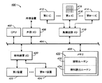
図19に、バス404を介し各種部材をCPU(中央処理ユニット)402に接続した構成を有するシステム400を示す。
FIG. 19 shows a
システム400は、共にバス404に接続された外部I/O(入出力部)406及びメモリ408を備えている。外部I/O406は、CPU402がシステム400外の装置と通信できるようにする部材である。
The
バス404にはこれら以外にも様々な部材が接続されている。まず、集積回路I/O410は、CPU402がアナライザ10内のICと通信できるようにする部材であり、この図にはICとして第0IC412から第M−1IC414に至るΜ個のICが示されている。また、それらIC412〜414はフォトセンサアレイを内蔵している。この図では、第mIC416の内部にフォトセンサアレイ418が描かれている。フォトセンサアレイ418は、先に述べた通り、それぞれ対応するサブレンジにて光子を検知する一群のセルを有している。同様に、照明装置I/O420もCPU402が各種照明装置と通信できるようにする部材であり、この図には照明装置として第0装置422から第N−1装置424に至るN個の装置が示されている。
Various members other than these are connected to the
メモリ408としてはプログラムメモリ430等が設けられている。プログラムメモリ430内には、図示の如く、照明ルーチン432、検知読出ルーチン434等のルーチンが格納されている。
As the
CPU402は、照明ルーチン432を実行して光源84や光源244と通信する。これにより、CPU402は、例えば種々のセンサから信号を受け取って計算を行い、どのような照明動作が必要かを計算結果に基づき判別し、そして光源84,244等に信号を供給してそれらを作動させる。
The
CPU402は、検知読出ルーチン434を実行することによって、上述のIC64、66、68、70、252、290等を含むIC412〜414内のセル群から、情報を取得する。例えば、CPU402から信号を供給して適当な検知周期の間に亘り光子の検知を実行させ、更にその結果を示す信号をIC内のセル群からCPU402が取得する。
The
以上例示説明した構成によれば、コンパクト且つ安価なコンポーネントが得られる。また、得られるコンポーネントを使用すれば分光分析等の機能を実現でき、その際、概ね、機械部品や光学部品を別途追加する必要もない。検知結果の読出は多数のICから迅速且つ並列的に行うことができ、従ってデータを高速で取得することができる。これは、物体の特徴を初期的に調査、特定する処理に利用できる。初期調査/特定の結果を利用すれば、その物体についてより細かな又はより立ち入った解析を行うべきかどうか、また別種解析を実施すべきかどうか、実施するとしたらどういう種類の解析か等を判別、決定することができる。このような多信号解析は試薬なしでの物体識別と相性がよく、また、この多信号解析によって様々な流体内に存する様々な物体を識別することができる。 According to the configuration described above as an example, a compact and inexpensive component can be obtained. Moreover, if the obtained component is used, functions such as spectroscopic analysis can be realized, and in that case, it is generally unnecessary to add mechanical parts and optical parts separately. Reading of the detection result can be performed quickly and in parallel from a large number of ICs, so that data can be acquired at high speed. This can be used for processing for initially investigating and specifying the characteristics of an object. Use initial survey / specific results to determine and decide whether to perform a more detailed or more in-depth analysis of the object, whether to perform a different type of analysis, and what type of analysis, if any. can do. Such multi-signal analysis is compatible with object identification without a reagent, and the multi-signal analysis can identify various objects existing in various fluids.
また、上述した各種の構成においては、概略、アナライザ内に複数個の検体を連続的に流し込むことができる。従って、リアルタイムな解析を行うことができ、またインタラクティブ検知方式も採用可能である。 Further, in the various configurations described above, generally, a plurality of specimens can be continuously poured into the analyzer. Accordingly, real-time analysis can be performed, and an interactive detection method can also be adopted.
また、以上説明した各種部材は、説明したものとは異なる様々な形状、寸法、特性数値、質的特性等を有し又は呈するものとすることができる。 The various members described above may have or exhibit various shapes, dimensions, characteristic numerical values, qualitative characteristics, and the like different from those described.
更に、上の説明では各種部材で特定の素材を使用した例を示したが、使用できる素材は数多くある。 Furthermore, in the above description, an example in which a specific material is used for various members is shown, but there are many materials that can be used.
以上の説明においては、流路付構造物に対し特定の形態でICを配置した例を示したが、流路付構造物に対するICの配置の仕方、設け方は説明したもの以外にも色々あろう。また、本発明にて使用するフォトセンサアレイは、本発明にてフォトセンサアレイとして使用するのに適切なものである限り、上述したものとは異なる種類のものであってもよい。例えば、ある単一のIC上にある単一の二次元フォトセンサアレイ内で、ある行と別の行とに別様の被覆を施し、別々の光子エネルギレンジにて光子検知を行わせるようにしてもよい。 In the above description, an example in which an IC is arranged in a specific form with respect to a structure with a flow path has been shown. Let's go. Further, the photosensor array used in the present invention may be of a different type from the above as long as it is suitable for use as a photosensor array in the present invention. For example, in a single two-dimensional photosensor array on a single IC, different coatings may be applied to one row and another to allow photon detection to occur at different photon energy ranges. May be.
また、上述した手法は、自己発光(self-emitting)乃至自発蛍光(auto-fluorescing)する物体例えば粒子に対しても適用できる。 The above-described method can also be applied to an object that emits self-emitting or auto-fluorescing, such as particles.
また、光標的間相互作用を強化できる手法は反共振光導波以外にも数多くある。また、それらの励起手法を経路沿いで実施する際、その場所は経路沿いの隣り合った場所とすることもできるし、実施場所間に距離を置くこともできる。更に、反共振光導波にまつわる各種パラメタを調整することも可能である。 In addition to the anti-resonant optical waveguide, there are many methods that can enhance the interaction between optical targets. Moreover, when performing these excitation methods along a path | route, the place can also be set as the adjacent place along a path | route, and can also put a distance between implementation places. Furthermore, it is possible to adjust various parameters related to the antiresonant optical waveguide.
また、図19に例示した構成ではCPUが用いられているが、これは、適当なものである限り、マイクロプロセッサその他の部材に置き換えてもよい。 Further, although a CPU is used in the configuration illustrated in FIG. 19, this may be replaced with a microprocessor or other members as long as it is appropriate.
上に例示した各種構成では、各種構成部材が特定の形態で動作するように製造及び使用されているが、説明した動作とは異なる動作を実行するようにしてもよいし、説明した順序とは異なる順序で動作を実行させてもよいし、説明外の動作を実行するようにしてもよい。 In the various configurations illustrated above, various components are manufactured and used so as to operate in a specific form. However, operations different from the operations described may be performed, and the order described Operations may be executed in a different order, or operations outside the description may be executed.
10 アナライザ、12 流路付構造物、14,294 チャネル、16,310,312,314 物体、64,66,68,70,290,412,414,416 IC(集積回路)、80,240 チャネル構成部分、86,322,324,326 蛍光・散乱光、87,252,292 検知器アセンブリ、90,92,94,122,160,162,296 チャネルを囲む物質、98,140,164,202,220 入射面(励起光結合部)、100,418 フォトセンサアレイ、106 サブレンジセル、126,128 光強度分布曲線、130,142,170,190,192,194,210,212,222,224 励起光、144 界面、150 インレットポート、152 アウトレットポート、180 流体可存在領域、182 空気存在領域、184,200 仕切部材、400 システム、402 CPU、432 照明ルーチン、434 検知読出ルーチン、α 仕切部材傾斜角、β,β’,γ’,γ”,φ,φ’ 入射角・伝搬角。
10 analyzer, 12 channel structure, 14,294 channel, 16,310,312,314 object, 64,66,68,70,290,412,414,416 IC (integrated circuit), 80,240 channel configuration 86,322,324,326 fluorescence, scattered light, 87,252,292 detector assembly, 90,92,94,122,160,162,296 material surrounding the channel, 98,140,164,202,220 Incident surface (excitation light coupling portion), 100, 418 photosensor array, 106 subrange cell, 126, 128 light intensity distribution curve, 130, 142, 170, 190, 192, 194, 210, 212, 222, 224
Claims (2)
前記チャネルは長手方向に伸び、長さに沿った何れの位置においても各断面を有し、各位置の断面において、前記チャネルの境界は、前記チャネル内の流体よりも高い屈折率を有する物質によってほぼ全体的に囲われ、
前記流体用構造物は前記チャネルに仕切部材を含み、前記仕切部材は光透過性部を含み、前記流体用構造物は、前記チャネルの境界に少なくとも部分的に沿った前記長手方向に、前記仕切部材を越えて前記チャネルの突出部へ伸びる光透過性部材をさらに含み、
前記光子検知方法は、
前記流路内に流体がある状態で、前記長さの一部に沿った断面において、伝搬する光のうち断面内強度比で約10%以上の部分が前記流体内を伝搬することとなるように前記流路を通して前記長手方向に光を伝搬させるステップであって、前記仕切部材を越えた前記光透過性部材と、前記チャネルの前記突出部と、前記仕切部材の前記光透過性部とを通して、前記チャネルの外部にある光源から光を供給するステップを含み、前記光源からの前記光は前記長手方向に対して斜めの方向から前記チャネルに入る、前記光を伝搬させるステップと、
前記伝搬する光に応じて前記チャネルから放出される光子を検知するステップと、
を含むことを特徴とする光子検知方法。 A photon detection method for detecting photons emitted from a channel formed in a fluid structure,
The channel extends in the longitudinal direction and has a cross section at any position along the length, in which the boundary of the channel is defined by a material having a higher refractive index than the fluid in the channel. Almost totally enclosed,
The fluid structure includes a partition member in the channel, the partition member includes a light transmissive portion, and the fluid structure includes the partition in the longitudinal direction at least partially along a boundary of the channel. A light transmissive member extending beyond the member to the protrusion of the channel;
The photon detection method is:
In a state where there is a fluid in the flow path, in the cross section along a part of the length, a portion of the propagating light having an intensity ratio in the cross section of about 10% or more propagates in the fluid. And propagating light in the longitudinal direction through the flow path through the light transmissive member beyond the partition member, the projecting portion of the channel, and the light transmissive portion of the partition member. Supplying light from a light source external to the channel, the light from the light source entering the channel from a direction oblique to the longitudinal direction, and propagating the light;
Detecting photons emitted from the channel in response to the propagating light;
A photon detection method comprising:
前記流体用構造物内に形成され、流体を含むことが可能なチャネルであって、前記チャネルは長手方向に伸び、長さに沿った何れの位置において も各断面を有し、各位置の断面において、前記チャネルの境界は、前記チャネル内の流体よりも高い屈折率を有する物質によってほぼ全体的に囲われる前記チャネルと、
前記流体用構造物の前記チャネルにある仕切部材であって、光透過性部を含む前記仕切部材と、
前記流体用構造物に含まれる光透過性部材であって、前記チャネルの境界に少なくとも部分的に沿った前記長手方向に、前記仕切部材を越えて前記チャネルの突出部へ伸びる光透過性部材と、
前記長手方向に前記チャネルを通って伝搬する光を供給する照明手段であって、前記長さの一部に沿った断面において、伝搬する光のうち断面内強度比で約10%以上の部分が前記流体内を伝搬することとなるように、前記照明手段は前記チャネルの外部から光を供給する光源を含み、前記光源は前記仕切部材を越えた前記光透過性部材と、前記チャネルの前記突出部と、前記仕切部材の前記光透過性部とを通して光を供給し、前記光源からの前記光は前記長手方向に対して斜めの方向から前記チャネルに入る前記照明手段と、
を含み、流体を含む前記チャネルに光を供給する装置。 Fluid structures;
A channel formed in the fluid structure and capable of containing fluid, the channel extending in a longitudinal direction and having a cross section at any position along the length, and a cross section at each position. Wherein the channel boundary is substantially entirely surrounded by a material having a higher refractive index than the fluid in the channel;
A partition member in the channel of the fluid structure, the partition member including a light transmissive portion;
A light transmissive member included in the fluid structure, wherein the light transmissive member extends in the longitudinal direction at least partially along a boundary of the channel and beyond the partition member to a protruding portion of the channel; ,
Illuminating means for supplying light propagating through the channel in the longitudinal direction, wherein in a cross section along a part of the length, a portion of the propagating light having an intensity ratio in the cross section of about 10% or more The illuminating means includes a light source that supplies light from outside the channel so that the light propagates through the fluid, and the light source includes the light transmissive member beyond the partition member and the protrusion of the channel. And the illumination means for supplying light through the light transmissive part of the partition member, and the light from the light source enters the channel from a direction oblique to the longitudinal direction;
And supplying light to the channel containing fluid.
Applications Claiming Priority (2)
| Application Number | Priority Date | Filing Date | Title |
|---|---|---|---|
| US11/316,660 US7386199B2 (en) | 2005-12-22 | 2005-12-22 | Providing light to channels or portions |
| US11/316,660 | 2005-12-22 |
Publications (3)
| Publication Number | Publication Date |
|---|---|
| JP2007171182A JP2007171182A (en) | 2007-07-05 |
| JP2007171182A5 JP2007171182A5 (en) | 2010-03-11 |
| JP5160776B2 true JP5160776B2 (en) | 2013-03-13 |
Family
ID=37876922
Family Applications (1)
| Application Number | Title | Priority Date | Filing Date |
|---|---|---|---|
| JP2006339568A Expired - Fee Related JP5160776B2 (en) | 2005-12-22 | 2006-12-18 | Photon detection method for detecting photons emitted from a channel and apparatus for supplying light to the channel |
Country Status (3)
| Country | Link |
|---|---|
| US (1) | US7386199B2 (en) |
| EP (1) | EP1801564B1 (en) |
| JP (1) | JP5160776B2 (en) |
Families Citing this family (57)
| Publication number | Priority date | Publication date | Assignee | Title |
|---|---|---|---|---|
| US7522786B2 (en) * | 2005-12-22 | 2009-04-21 | Palo Alto Research Center Incorporated | Transmitting light with photon energy information |
| US7310153B2 (en) | 2004-08-23 | 2007-12-18 | Palo Alto Research Center, Incorporated | Using position-sensitive detectors for wavelength determination |
| US7386199B2 (en) | 2005-12-22 | 2008-06-10 | Palo Alto Research Center Incorporated | Providing light to channels or portions |
| US7420677B2 (en) * | 2005-12-22 | 2008-09-02 | Palo Alto Research Center Incorporated | Sensing photon energies of optical signals |
| US7315667B2 (en) * | 2005-12-22 | 2008-01-01 | Palo Alto Research Center Incorporated | Propagating light to be sensed |
| US7547904B2 (en) * | 2005-12-22 | 2009-06-16 | Palo Alto Research Center Incorporated | Sensing photon energies emanating from channels or moving objects |
| US8437582B2 (en) * | 2005-12-22 | 2013-05-07 | Palo Alto Research Center Incorporated | Transmitting light with lateral variation |
| US7358476B2 (en) * | 2005-12-22 | 2008-04-15 | Palo Alto Research Center Incorporated | Sensing photons from objects in channels |
| US7718948B2 (en) * | 2006-12-04 | 2010-05-18 | Palo Alto Research Center Incorporated | Monitoring light pulses |
| US9164037B2 (en) | 2007-01-26 | 2015-10-20 | Palo Alto Research Center Incorporated | Method and system for evaluation of signals received from spatially modulated excitation and emission to accurately determine particle positions and distances |
| US8821799B2 (en) | 2007-01-26 | 2014-09-02 | Palo Alto Research Center Incorporated | Method and system implementing spatially modulated excitation or emission for particle characterization with enhanced sensitivity |
| US7554673B2 (en) * | 2007-02-05 | 2009-06-30 | Palo Alto Research Center Incorporated | Obtaining information about analytes using optical cavity output light |
| US7936463B2 (en) | 2007-02-05 | 2011-05-03 | Palo Alto Research Center Incorporated | Containing analyte in optical cavity structures |
| US7545513B2 (en) * | 2007-02-05 | 2009-06-09 | Palo Alto Research Center Incorporated | Encoding optical cavity output light |
| US7633629B2 (en) | 2007-02-05 | 2009-12-15 | Palo Alto Research Center Incorporated | Tuning optical cavities |
| US7817276B2 (en) | 2007-02-05 | 2010-10-19 | Palo Alto Research Center Incorporated | Distinguishing objects |
| US7502123B2 (en) * | 2007-02-05 | 2009-03-10 | Palo Alto Research Center Incorporated | Obtaining information from optical cavity output light |
| US7522811B2 (en) * | 2007-07-13 | 2009-04-21 | Palo Alto Research Center Incorporated | Producing sandwich waveguides |
| US7529438B2 (en) * | 2007-07-13 | 2009-05-05 | Palo Alto Research Center Incorporated | Producing fluidic waveguides |
| US7822300B2 (en) * | 2007-11-20 | 2010-10-26 | Aptina Imaging Corporation | Anti-resonant reflecting optical waveguide for imager light pipe |
| US8320983B2 (en) * | 2007-12-17 | 2012-11-27 | Palo Alto Research Center Incorporated | Controlling transfer of objects affecting optical characteristics |
| US7817254B2 (en) * | 2008-01-30 | 2010-10-19 | Palo Alto Research Center Incorporated | Obtaining information from time variation of sensing results |
| JP5503154B2 (en) * | 2008-01-30 | 2014-05-28 | パロ・アルト・リサーチ・センター・インコーポレーテッド | System and method for causing non-uniform relative motion of an object within a transform zone |
| EP2085797B1 (en) | 2008-01-30 | 2016-06-01 | Palo Alto Research Center Incorporated | Producing Filters with Combined Transmission and/or Reflection Functions |
| EP2085760B1 (en) | 2008-01-30 | 2018-07-04 | Palo Alto Research Center Incorporated | Producing time variation in emanating light |
| US8153950B2 (en) * | 2008-12-18 | 2012-04-10 | Palo Alto Research Center Incorporated | Obtaining sensing results and/or data in response to object detection |
| US8153949B2 (en) * | 2008-12-18 | 2012-04-10 | Palo Alto Research Center Incorporated | Obtaining sensing results indicating time variation |
| US7763856B2 (en) * | 2008-01-31 | 2010-07-27 | Palo Alto Research Center Incorporated | Producing time variation in emanating light |
| JP5541764B2 (en) | 2008-01-30 | 2014-07-09 | パロ・アルト・リサーチ・センター・インコーポレーテッド | Apparatus and method for acquiring information in response to object detection |
| US7894068B2 (en) * | 2008-02-04 | 2011-02-22 | Palo Alto Research Center Incorporated | Producing filters with combined transmission and/or reflection functions |
| EP2085762B1 (en) | 2008-01-30 | 2018-07-04 | Palo Alto Research Center Incorporated | Transmitting/reflecting emanating light with time variation |
| US7701580B2 (en) * | 2008-02-01 | 2010-04-20 | Palo Alto Research Center Incorporated | Transmitting/reflecting emanating light with time variation |
| JP5620642B2 (en) | 2008-01-30 | 2014-11-05 | パロ・アルト・リサーチ・センター・インコーポレーテッドPaloAlto ResearchCenterIncorporated | Method using sensor with encoder, sensor and system with encoder |
| US8373860B2 (en) | 2008-02-01 | 2013-02-12 | Palo Alto Research Center Incorporated | Transmitting/reflecting emanating light with time variation |
| US8629981B2 (en) | 2008-02-01 | 2014-01-14 | Palo Alto Research Center Incorporated | Analyzers with time variation based on color-coded spatial modulation |
| US9658222B2 (en) | 2009-03-02 | 2017-05-23 | Mbio Diagnostics, Inc. | Planar waveguide based cartridges and associated methods for detecting target analyte |
| US8586347B2 (en) | 2010-09-15 | 2013-11-19 | Mbio Diagnostics, Inc. | System and method for detecting multiple molecules in one assay |
| US8331751B2 (en) * | 2009-03-02 | 2012-12-11 | mBio Diagnositcs, Inc. | Planar optical waveguide with core of low-index-of-refraction interrogation medium |
| US9212995B2 (en) | 2009-03-02 | 2015-12-15 | Mbio Diagnostics, Inc. | System and method for detecting multiple molecules in one assay |
| JP4927197B2 (en) * | 2010-06-01 | 2012-05-09 | シャープ株式会社 | Micro-analysis chip, analyzer using the micro-analysis chip, and liquid feeding method |
| GB201016270D0 (en) * | 2010-09-28 | 2010-11-10 | Univ St Andrews | Waveguide localised raman spectroscopy |
| US10114020B2 (en) | 2010-10-11 | 2018-10-30 | Mbio Diagnostics, Inc. | System and device for analyzing a fluidic sample |
| US8723140B2 (en) | 2011-08-09 | 2014-05-13 | Palo Alto Research Center Incorporated | Particle analyzer with spatial modulation and long lifetime bioprobes |
| US9029800B2 (en) | 2011-08-09 | 2015-05-12 | Palo Alto Research Center Incorporated | Compact analyzer with spatial modulation and multiple intensity modulated excitation sources |
| JP5988690B2 (en) * | 2012-05-18 | 2016-09-07 | 浜松ホトニクス株式会社 | Spectroscopic sensor |
| JP5875936B2 (en) | 2012-05-18 | 2016-03-02 | 浜松ホトニクス株式会社 | Spectroscopic sensor |
| EP2911791A4 (en) | 2012-10-29 | 2016-11-02 | Mbio Diagnostics Inc | Biological particle identification system, cartridge and associated methods |
| US9551617B2 (en) * | 2013-07-11 | 2017-01-24 | Shimadzu Corporation | Raman spectroscopic analyzer |
| US9207066B2 (en) | 2014-02-14 | 2015-12-08 | Palo Alto Research Center Incorporated | Spatial modulation of light to determine dimensional characteristics of objects in a flow path |
| US10451482B2 (en) | 2014-02-14 | 2019-10-22 | Palo Alto Research Center Incorporated | Determination of color characteristics of objects using spatially modulated light |
| US9952033B2 (en) | 2014-02-14 | 2018-04-24 | Palo Alto Research Center Incorporated | Spatial modulation of light to determine object length |
| US9528925B2 (en) | 2014-02-14 | 2016-12-27 | Palo Alto Research Center Incorporated | Spatial modulation of light to determine object position |
| US9400174B2 (en) | 2014-04-07 | 2016-07-26 | Palo Alto Research Center Incorporated | Monitor for particle injector |
| US9114606B1 (en) | 2014-04-07 | 2015-08-25 | Palo Alto Research Center Incorporated | Spatial light modulation method for determining droplet motion characteristics |
| US20210231567A1 (en) * | 2018-07-31 | 2021-07-29 | Institut Für Bioprozess- Und Analysenmesstechnik E. V. | Device and methods for optically characterizing fluids and/or objects enclosed therein in microchannels |
| US10458909B1 (en) | 2018-10-24 | 2019-10-29 | International Business Machines Corporation | MEMS optical sensor |
| US20230175891A1 (en) * | 2021-12-08 | 2023-06-08 | Battelle Savannah River Alliance, Llc | Electric field detection method and system |
Family Cites Families (102)
| Publication number | Priority date | Publication date | Assignee | Title |
|---|---|---|---|---|
| US2708389A (en) | 1951-01-09 | 1955-05-17 | Frederick W Kavanagh | Spectral wedge interference filter combined with purifying filters |
| US3797911A (en) * | 1972-10-18 | 1974-03-19 | Bell Telephone Labor Inc | Thin film optical couplers employing mode conversion |
| US3973118A (en) | 1975-03-25 | 1976-08-03 | Lamontagne Joseph Alfred | Electro-optical detector array and spectrum analyzer system |
| US4081277A (en) | 1976-10-08 | 1978-03-28 | Eastman Kodak Company | Method for making a solid-state color imaging device having an integral color filter and the device |
| SE450528B (en) | 1981-03-19 | 1987-06-29 | Svenska Traeforskningsinst | PROCEDURE FOR SEATING THE CONTENT OF CURRENCY IN PAPER Pulp |
| US4573796A (en) | 1984-01-06 | 1986-03-04 | The United States Of America As Represented By The United States Department Of Energy | Apparatus for eliminating background interference in fluorescence measurements |
| US4715672A (en) * | 1986-01-06 | 1987-12-29 | American Telephone And Telegraph Company | Optical waveguide utilizing an antiresonant layered structure |
| CA1293879C (en) | 1986-06-20 | 1992-01-07 | Laurel Jean Pace | Color filter arrays |
| US4957371A (en) | 1987-12-11 | 1990-09-18 | Santa Barbara Research Center | Wedge-filter spectrometer |
| US4976542A (en) | 1988-07-25 | 1990-12-11 | Washington University | Digital array scanned interferometer |
| JPH0249143A (en) * | 1988-08-11 | 1990-02-19 | Ngk Spark Plug Co Ltd | Detector for liquid mixing ratio of mixed liquid |
| JPH0249144A (en) * | 1988-08-11 | 1990-02-19 | Ngk Spark Plug Co Ltd | Detector for liquid mixing ratio of mixed liquid |
| US5080462A (en) | 1989-11-02 | 1992-01-14 | Fuji Photo Film Co., Ltd. | Optical wavelength converter device and optical wavelength converter system |
| US5144498A (en) | 1990-02-14 | 1992-09-01 | Hewlett-Packard Company | Variable wavelength light filter and sensor system |
| US5166755A (en) | 1990-05-23 | 1992-11-24 | Nahum Gat | Spectrometer apparatus |
| US5784507A (en) | 1991-04-05 | 1998-07-21 | Holm-Kennedy; James W. | Integrated optical wavelength discrimination devices and methods for fabricating same |
| US5184192A (en) * | 1991-07-17 | 1993-02-02 | Millipore Corporation | Photometric apparatus with a flow cell coated with an amorphous fluoropolymer |
| US5370842A (en) | 1991-11-29 | 1994-12-06 | Canon Kabushiki Kaisha | Sample measuring device and sample measuring system |
| US5305082A (en) | 1992-01-08 | 1994-04-19 | Chromax, Inc. | High spatial resolution imaging spectrograph |
| US5324401A (en) * | 1993-02-05 | 1994-06-28 | Iowa State University Research Foundation, Inc. | Multiplexed fluorescence detector system for capillary electrophoresis |
| US5494798A (en) * | 1993-12-09 | 1996-02-27 | Gerdt; David W. | Fiber optic evanscent wave sensor for immunoassay |
| WO1995020144A1 (en) | 1994-01-20 | 1995-07-27 | British Telecommunications Public Limited Company | Optical wavelength sensor |
| DE69405087T2 (en) | 1994-04-27 | 1997-12-18 | Hewlett Packard Gmbh | Optical detector |
| US6199257B1 (en) * | 1995-02-28 | 2001-03-13 | Thermo Separation Products, Inc. | Method of making a flow cell for light absorption measurement of small volume samples |
| US5682038A (en) | 1995-04-06 | 1997-10-28 | Becton Dickinson And Company | Fluorescent-particle analyzer with timing alignment for analog pulse subtraction of fluorescent pulses arising from different excitation locations |
| US5777329A (en) | 1995-07-21 | 1998-07-07 | Texas Instruments Incorporated | Bolometer array spectrometer |
| EP0762119B1 (en) * | 1995-09-06 | 2001-12-05 | Agilent Technologies Deutschland GmbH | Photometric flow apparatus for small sample volumes |
| AU2335297A (en) * | 1996-03-19 | 1997-10-10 | University Of Utah Research Foundation | Lens and associatable flow cell |
| US5770156A (en) | 1996-06-04 | 1998-06-23 | In Usa, Inc. | Gas detection and measurement system |
| US5801831A (en) | 1996-09-20 | 1998-09-01 | Institute For Space And Terrestrial Science | Fabry-Perot spectrometer for detecting a spatially varying spectral signature of an extended source |
| US5792663A (en) | 1996-09-27 | 1998-08-11 | Transgenomic Incorporated | High efficiency continuous flow through fractional-volatilization separator system, and method of use |
| US6490034B1 (en) | 1996-11-18 | 2002-12-03 | Fraunhofer-Gesellschaft Zur Foerderung Der Angewandten Forschung E.V. | Micromechanical transmission measuring cell |
| US5864641A (en) | 1997-04-11 | 1999-01-26 | F&S, Inc. | Optical fiber long period sensor having a reactive coating |
| US6238348B1 (en) | 1997-07-22 | 2001-05-29 | Scimed Life Systems, Inc. | Miniature spectrometer system and method |
| US5880474A (en) | 1997-08-29 | 1999-03-09 | Becton Dickinson And Company | Multi-illumination-source flow particle analyzer with inter-location emissions crosstalk cancelation |
| DE19754910C2 (en) | 1997-12-10 | 1999-12-02 | Geoforschungszentrum Potsdam | Wavelength detection on fiber Bragg grating sensors |
| GB9803704D0 (en) | 1998-02-24 | 1998-04-15 | Univ Manchester | Waveguide structure |
| US6719868B1 (en) | 1998-03-23 | 2004-04-13 | President And Fellows Of Harvard College | Methods for fabricating microfluidic structures |
| US6459080B1 (en) | 1998-06-12 | 2002-10-01 | Agilent Technologies, Inc. | Miniaturized device for separating the constituents of a sample and delivering the constituents of the separated sample to a mass spectrometer |
| US7737088B1 (en) | 1998-08-28 | 2010-06-15 | Febit Holding Gmbh | Method and device for producing biochemical reaction supporting materials |
| US6275628B1 (en) | 1998-12-10 | 2001-08-14 | Luna Innovations, Inc. | Single-ended long period grating optical device |
| US6249346B1 (en) | 1998-12-21 | 2001-06-19 | Xerox Corporation | Monolithic spectrophotometer |
| US6608679B1 (en) | 1998-12-21 | 2003-08-19 | Xerox Corporation | Spectrophotometric analysis of input light |
| US6399405B1 (en) | 1998-12-21 | 2002-06-04 | Xerox Corporation | Process for constructing a spectrophotometer |
| EP1031828B1 (en) | 1999-02-25 | 2006-09-13 | C.S.E.M. Centre Suisse D'electronique Et De Microtechnique Sa | Integrated-optical sensor and method for integrated-optically sensing a substance |
| US6558945B1 (en) | 1999-03-08 | 2003-05-06 | Aclara Biosciences, Inc. | Method and device for rapid color detection |
| US6455833B1 (en) | 1999-03-09 | 2002-09-24 | Micron Technology, Inc. | Superposed multi-junction color APS |
| JP3530078B2 (en) * | 1999-07-06 | 2004-05-24 | リオン株式会社 | Flow cell and particle measuring apparatus using the flow cell |
| US6192168B1 (en) | 1999-04-09 | 2001-02-20 | The United States Of America As Represented By The Secretary Of The Navy | Reflectively coated optical waveguide and fluidics cell integration |
| AU4128500A (en) | 1999-04-09 | 2000-11-14 | University Of Manchester Institute Of Science & Technology, The | Electrophoresis method and apparatus with time- or space-modulated sample injection |
| US6137117A (en) | 1999-06-21 | 2000-10-24 | The United States Of America As Represented By The Secretary Of The Navy | Integrating multi-waveguide sensor |
| US6353475B1 (en) | 1999-07-12 | 2002-03-05 | Caliper Technologies Corp. | Light source power modulation for use with chemical and biochemical analysis |
| US6495104B1 (en) | 1999-08-19 | 2002-12-17 | Caliper Technologies Corp. | Indicator components for microfluidic systems |
| US6216022B1 (en) | 2000-06-22 | 2001-04-10 | Biosafe Laboratories, Inc. | Implantable optical measurement device and method for using same |
| US7167615B1 (en) | 1999-11-05 | 2007-01-23 | Board Of Regents, The University Of Texas System | Resonant waveguide-grating filters and sensors and methods for making and using same |
| US6603548B2 (en) | 1999-12-03 | 2003-08-05 | Sciperio, Inc. | Biosensor |
| US6295130B1 (en) | 1999-12-22 | 2001-09-25 | Xerox Corporation | Structure and method for a microelectromechanically tunable fabry-perot cavity spectrophotometer |
| US6519037B2 (en) | 1999-12-23 | 2003-02-11 | Lj Laboratories, Llc | Spectrometer having optical unit including a randomized fiber optic implement |
| US6580507B2 (en) | 2000-03-02 | 2003-06-17 | Sd Acquisition Inc. | Single source, single detector chip, multiple-longitudinal channel electromagnetic radiation absorbance and fluorescence monitoring system |
| US6569383B1 (en) | 2000-03-11 | 2003-05-27 | Intrinsic Bioprobes, Inc. | Bioactive chip mass spectrometry |
| US6505775B1 (en) | 2000-04-25 | 2003-01-14 | Ncr Corporation | Produce data collector with enhanced LVF spectrometer |
| WO2002021110A1 (en) | 2000-09-04 | 2002-03-14 | Zeptosens Ag | Multianalyte determination system and methods |
| GB0023041D0 (en) | 2000-09-20 | 2000-11-01 | Univ Manchester | Identification apparatus |
| WO2002025934A2 (en) | 2000-09-25 | 2002-03-28 | Sensovation Ag | Image sensor device, apparatus and method for optical measurements |
| US7264973B2 (en) | 2000-10-30 | 2007-09-04 | Sru Biosystems, Inc. | Label-free methods for performing assays using a colorimetric resonant optical biosensor |
| US7217574B2 (en) | 2000-10-30 | 2007-05-15 | Sru Biosystems, Inc. | Method and apparatus for biosensor spectral shift detection |
| US6577780B2 (en) | 2001-03-08 | 2003-06-10 | Veridian Systems | Cell designs for optical biosensors |
| US6785002B2 (en) | 2001-03-16 | 2004-08-31 | Optical Coating Laboratory, Inc. | Variable filter-based optical spectrometer |
| US6630999B2 (en) | 2001-05-01 | 2003-10-07 | Optical Coating Laboratory, Inc. | Color measuring sensor assembly for spectrometer devices |
| EP1493487A1 (en) | 2001-06-28 | 2005-01-05 | Agilent Technologies, Inc. | Microfluidic system with ESI residual current control |
| US6934435B2 (en) | 2001-10-05 | 2005-08-23 | ARETé ASSOCIATES | Microfluidic pump system for chemical or biological agents |
| US20050042615A1 (en) | 2001-11-02 | 2005-02-24 | Smith William Ewen | Microfluidic ser(r)s detection |
| US6800849B2 (en) | 2001-12-19 | 2004-10-05 | Sau Lan Tang Staats | Microfluidic array devices and methods of manufacture and uses thereof |
| US7524459B2 (en) | 2002-01-24 | 2009-04-28 | California Institute Of Technology In Pasadena | Optoelectronic and microfluidic integration for miniaturized spectroscopic devices |
| AU2003213294A1 (en) * | 2002-02-25 | 2003-09-09 | Waters Investments Limited | An opaque additive to block stray light in teflon af light-guiding flowcells |
| JP2003279471A (en) * | 2002-03-20 | 2003-10-02 | Nippon Sheet Glass Co Ltd | Chip for microchemical system and microchemical system |
| US6867420B2 (en) | 2002-06-03 | 2005-03-15 | The Regents Of The University Of California | Solid-state detector and optical system for microchip analyzers |
| US6700664B1 (en) | 2002-08-15 | 2004-03-02 | Jds Uniphase Corporation | Optical channel monitoring device |
| DE60212620T2 (en) | 2002-08-16 | 2006-11-02 | Agilent Technologies, Inc. (n.d.Ges.d.Staates Delaware), Palo Alto | Method and apparatus for analyzing a sample mixture |
| US20040067167A1 (en) | 2002-10-08 | 2004-04-08 | Genoptix, Inc. | Methods and apparatus for optophoretic diagnosis of cells and particles |
| US7106441B2 (en) | 2002-10-28 | 2006-09-12 | Xerox Corporation | Structure and method for a microelectromechanic cylindrical reflective diffraction grating spectrophotometer |
| US7064836B2 (en) | 2003-04-21 | 2006-06-20 | The Board Of Trustees Of The Leland Stanford Junior University | Brewster's angle flow cell for cavity ring-down spectroscopy |
| US7497992B2 (en) | 2003-05-08 | 2009-03-03 | Sru Biosystems, Inc. | Detection of biochemical interactions on a biosensor using tunable filters and tunable lasers |
| US7262845B2 (en) | 2003-05-27 | 2007-08-28 | Wayne State University | Diffractive imaging spectrometer |
| WO2004113957A2 (en) | 2003-06-16 | 2004-12-29 | The Regents Of The University Of California | Apparatus for optical measurements on low-index non-solid materials based on arrow waveguides |
| US7298478B2 (en) | 2003-08-14 | 2007-11-20 | Cytonome, Inc. | Optical detector for a particle sorting system |
| JP2005170803A (en) * | 2003-12-08 | 2005-06-30 | Daicel Chem Ind Ltd | New monomethyl malonate derivative and method for producing the same |
| WO2006007878A1 (en) | 2004-07-22 | 2006-01-26 | Agilent Technologies, Inc. | Micrrofluidic arrangement for microfluidic optical detection |
| US7310153B2 (en) | 2004-08-23 | 2007-12-18 | Palo Alto Research Center, Incorporated | Using position-sensitive detectors for wavelength determination |
| US7291824B2 (en) | 2005-12-22 | 2007-11-06 | Palo Alto Research Center Incorporated | Photosensing throughout energy range and in subranges |
| US7522786B2 (en) | 2005-12-22 | 2009-04-21 | Palo Alto Research Center Incorporated | Transmitting light with photon energy information |
| US7387892B2 (en) | 2004-09-01 | 2008-06-17 | Palo Alto Research Center Incorporated | Biosensor using microdisk laser |
| US7268868B2 (en) * | 2004-10-29 | 2007-09-11 | Palo Alto Research Center Incorporated | Anti-resonant waveguide sensors |
| US7811438B2 (en) | 2004-12-08 | 2010-10-12 | Palo Alto Research Center Incorporated | Bio-enrichment device to enhance sample collection and detection |
| US7466409B2 (en) | 2005-06-08 | 2008-12-16 | California Institute Of Technology | Method and apparatus for CMOS imagers and spectroscopy |
| US7420677B2 (en) * | 2005-12-22 | 2008-09-02 | Palo Alto Research Center Incorporated | Sensing photon energies of optical signals |
| US7433552B2 (en) | 2005-12-22 | 2008-10-07 | Palo Alto Research Center Incorporated | Obtaining analyte information |
| US7315667B2 (en) | 2005-12-22 | 2008-01-01 | Palo Alto Research Center Incorporated | Propagating light to be sensed |
| US7358476B2 (en) | 2005-12-22 | 2008-04-15 | Palo Alto Research Center Incorporated | Sensing photons from objects in channels |
| US7386199B2 (en) | 2005-12-22 | 2008-06-10 | Palo Alto Research Center Incorporated | Providing light to channels or portions |
| US7248361B2 (en) | 2005-12-22 | 2007-07-24 | Palo Alto Research Center Incorporated | Fluorescence reader based on anti-resonant waveguide excitation |
| US7547904B2 (en) | 2005-12-22 | 2009-06-16 | Palo Alto Research Center Incorporated | Sensing photon energies emanating from channels or moving objects |
-
2005
- 2005-12-22 US US11/316,660 patent/US7386199B2/en active Active
-
2006
- 2006-12-18 JP JP2006339568A patent/JP5160776B2/en not_active Expired - Fee Related
- 2006-12-19 EP EP06126528.6A patent/EP1801564B1/en not_active Expired - Fee Related
Also Published As
| Publication number | Publication date |
|---|---|
| JP2007171182A (en) | 2007-07-05 |
| EP1801564A1 (en) | 2007-06-27 |
| US20070147728A1 (en) | 2007-06-28 |
| EP1801564B1 (en) | 2018-06-20 |
| US7386199B2 (en) | 2008-06-10 |
Similar Documents
| Publication | Publication Date | Title |
|---|---|---|
| JP5160776B2 (en) | Photon detection method for detecting photons emitted from a channel and apparatus for supplying light to the channel | |
| JP5329753B2 (en) | Sensor and object photon detection method in path | |
| JP2007171189A (en) | Detection device for photons from matter inside channel | |
| JP5495474B2 (en) | Photon detection per subrange within photon energy range | |
| TWI383139B (en) | Tubular waveguide type plasma resonance sensing device and sensing system | |
| JP3816072B2 (en) | Optical waveguide sensor and measuring device using the same | |
| US7529438B2 (en) | Producing fluidic waveguides | |
| US6480282B1 (en) | Capillary surface plasmon resonance sensors and multisensors | |
| US7522811B2 (en) | Producing sandwich waveguides | |
| US8940523B2 (en) | Pipette tip, pipette system and method for performing analysis with the pipette tip and system | |
| JP2008191147A (en) | Optical cavity device, and method for sensing optical cavity output light | |
| EP2726852B1 (en) | Multiple examinations of a sample | |
| US20160011112A1 (en) | Sample Plate and Analyzing Method | |
| US20230017547A1 (en) | Digital microfluidic (dmf) system, dmf cartridge, and method including integrated optical fiber sensing | |
| CN101738385B (en) | Tubular waveguide type plasmon resonance sensing device and sensing system | |
| JP2004077411A (en) | Surface plasmon sensor and spr device | |
| WO2012132313A1 (en) | Immunoassay device | |
| US20110236262A1 (en) | Biological substance detecting apparatus | |
| CN110546480A (en) | Lateral detection of fluid properties | |
| EP3638109B1 (en) | Method for determining the concentration of an analyte in whole blood | |
| JP2020190521A (en) | Surface plasmon resonance sensor device |
Legal Events
| Date | Code | Title | Description |
|---|---|---|---|
| A621 | Written request for application examination |
Free format text: JAPANESE INTERMEDIATE CODE: A621 Effective date: 20091217 |
|
| A521 | Written amendment |
Free format text: JAPANESE INTERMEDIATE CODE: A523 Effective date: 20100126 |
|
| A131 | Notification of reasons for refusal |
Free format text: JAPANESE INTERMEDIATE CODE: A131 Effective date: 20120717 |
|
| A521 | Written amendment |
Free format text: JAPANESE INTERMEDIATE CODE: A523 Effective date: 20121016 |
|
| TRDD | Decision of grant or rejection written | ||
| A01 | Written decision to grant a patent or to grant a registration (utility model) |
Free format text: JAPANESE INTERMEDIATE CODE: A01 Effective date: 20121120 |
|
| A61 | First payment of annual fees (during grant procedure) |
Free format text: JAPANESE INTERMEDIATE CODE: A61 Effective date: 20121213 |
|
| R150 | Certificate of patent or registration of utility model |
Ref document number: 5160776 Country of ref document: JP Free format text: JAPANESE INTERMEDIATE CODE: R150 Free format text: JAPANESE INTERMEDIATE CODE: R150 |
|
| FPAY | Renewal fee payment (event date is renewal date of database) |
Free format text: PAYMENT UNTIL: 20151221 Year of fee payment: 3 |
|
| R250 | Receipt of annual fees |
Free format text: JAPANESE INTERMEDIATE CODE: R250 |
|
| R250 | Receipt of annual fees |
Free format text: JAPANESE INTERMEDIATE CODE: R250 |
|
| R250 | Receipt of annual fees |
Free format text: JAPANESE INTERMEDIATE CODE: R250 |
|
| R250 | Receipt of annual fees |
Free format text: JAPANESE INTERMEDIATE CODE: R250 |
|
| R250 | Receipt of annual fees |
Free format text: JAPANESE INTERMEDIATE CODE: R250 |
|
| LAPS | Cancellation because of no payment of annual fees |