JP5148126B2 - Color conversion light emitting device and manufacturing method thereof - Google Patents
Color conversion light emitting device and manufacturing method thereof Download PDFInfo
- Publication number
- JP5148126B2 JP5148126B2 JP2007030226A JP2007030226A JP5148126B2 JP 5148126 B2 JP5148126 B2 JP 5148126B2 JP 2007030226 A JP2007030226 A JP 2007030226A JP 2007030226 A JP2007030226 A JP 2007030226A JP 5148126 B2 JP5148126 B2 JP 5148126B2
- Authority
- JP
- Japan
- Prior art keywords
- light emitting
- light
- emitting element
- emitting device
- frame portion
- Prior art date
- Legal status (The legal status is an assumption and is not a legal conclusion. Google has not performed a legal analysis and makes no representation as to the accuracy of the status listed.)
- Expired - Fee Related
Links
Images


Landscapes
- Led Device Packages (AREA)
- Led Devices (AREA)
Description
本発明は、発光ダイオード(以下、LED)からの発光を蛍光体によって変換して他の波長の光を得る、波長変換型発光素子に関する。 The present invention relates to a wavelength conversion type light emitting device that converts light emitted from a light emitting diode (hereinafter referred to as LED) by a phosphor to obtain light of other wavelengths.
近年、紫外又は青色LED等に、LEDからの発光を他の波長に変換する蛍光体とを組合せて白色光を得る、いわゆる白色LEDが広く使用されている。使用されている製品は、例えば、液晶用バックライトや小型照明等である。 In recent years, so-called white LEDs that obtain white light by combining ultraviolet or blue LEDs and the like with phosphors that convert light emitted from the LEDs into other wavelengths have been widely used. The products used are, for example, liquid crystal backlights and small illuminations.
白色LEDは、見る方向によって色が変わる、いわゆる色むらの発生を防止するため、蛍光体層を均一に形成する技術がいくつか開発されている。 In order to prevent the occurrence of so-called color unevenness, in which the color of the white LED changes depending on the viewing direction, several techniques for uniformly forming the phosphor layer have been developed.
特許文献1には、LEDチップの上に、別体に形成した蛍光体チップを配置し、爪で係合するものが開示されている。従って、蛍光体チップを発光素子に押し付け、固定できる利点がある。
上記文献は、いずれも蛍光体チップをLEDチップ上に戴置するものである。しかし、LEDチップ及び蛍光体チップのいずれも1mm角より小さく、戴置工程の際に位置合わせに時間がかかるという問題がある。 In any of the above documents, a phosphor chip is placed on an LED chip. However, both the LED chip and the phosphor chip are smaller than 1 mm square, and there is a problem that it takes time for alignment in the placing process.
上記課題は、光学機能層と、前記光学機能層外周を囲み、位置合わせ構造を形成された枠部と、発光素子と、を含み、前記発光素子に、前記枠部と前記光学機能層が前記位置合わせ構造によって位置合わせがされた状態で戴置されていることを特徴とする、本発明の発光装置の構成により、解決される。 The subject includes an optical function layer, a frame portion that surrounds the outer periphery of the optical function layer and has an alignment structure, and a light emitting element, and the light emitting element includes the frame portion and the optical function layer. This is solved by the structure of the light emitting device of the present invention, which is placed in a state of being aligned by the alignment structure.
また、枠部は、発光素子との間に電気的接続部を形成してもよい。この場合、更に外部の電源等の電気回路に接続するため、外部接続端子を形成する。 The frame part may form an electrical connection part between the light emitting element. In this case, an external connection terminal is formed for further connection to an electric circuit such as an external power source.
また、枠部がシリコンによって形成された場合、発光素子との間に電気的接続部を設け、更に、既知の半導体プロセスによってコンデンサやダイオード等の発光素子のための静電保護素子を形成してもよい。 In addition, when the frame portion is formed of silicon, an electrical connection portion is provided between the frame and the light-emitting element, and an electrostatic protection element for the light-emitting element such as a capacitor or a diode is formed by a known semiconductor process. Also good.
また、上記課題は、本発明の別の観点によれば、光学機能層と、前記光学機能層外周を囲み、位置合わせ構造を形成された枠部と、半導体発光素子と、を含み、前記発光素子に、前記枠部と前記光学機能層が前記位置合わせ構造によって位置合わせがされた状態で戴置する発光装置の製造方法であって、オーミック電極を表面に形成した個片化した前記半導体発光素子を準備する工程と、ウエハ基板に複数の開口部および前記位置合わせ構造を形成して複数の枠部を一体に形成する工程と、前記開口部内に、開口部の深さに応じた一定の膜厚の光学機能層を充填し、その後に枠部を個片とする工程を有することを特徴とする発光装置の製造方法により、解決される。
According to another aspect of the present invention, the above object includes an optical functional layer, a frame portion that surrounds the outer periphery of the optical functional layer and has an alignment structure, and a semiconductor light emitting element, and the light emission A method of manufacturing a light-emitting device in which an element is placed in a state in which the frame portion and the optical functional layer are aligned by the alignment structure, wherein the semiconductor light-emitting device is divided into pieces with an ohmic electrode formed on a surface thereof A step of preparing an element, a step of forming a plurality of openings and the alignment structure on the wafer substrate to integrally form a plurality of frames, and a constant amount in the opening according to the depth of the opening This is solved by a method for manufacturing a light-emitting device, which includes a step of filling an optical functional layer with a film thickness and then making the frame part into pieces.
本発明の構成により、光学機能層を保持する枠部を発光素子上に戴置する際に、位置合わせが簡単となり、時間を要しないと言う効果がある。 According to the configuration of the present invention, when the frame portion holding the optical function layer is placed on the light emitting element, there is an effect that positioning is simplified and time is not required.
光学機能層に、発光素子からの発光を受けて、その発光波長より長波長の蛍光を発する蛍光体を含むことで、例えば発光素子からの発光と蛍光体からの発光の両者の混合光を得ることができる。例えば発光素子として青色LEDを用い、蛍光体として青色光を吸収して黄色い蛍光を発するYAG:Ce蛍光体を使用することで白色光を得る等が考えられる。 The optical functional layer includes a phosphor that receives light emitted from the light emitting element and emits fluorescence having a wavelength longer than the light emission wavelength, thereby obtaining, for example, a mixed light of both light emitted from the light emitting element and light emitted from the phosphor. be able to. For example, it is possible to obtain white light by using a blue LED as a light emitting element and using a YAG: Ce phosphor that absorbs blue light and emits yellow fluorescence as a phosphor.
光学機能層に、発光素子からの発光を受けて、その光を散乱する散乱材を含むことで、発光素子面内の発光むらの影響を緩和し、均一な発光面を得ることができる。例えば、発光素子として、大きさが1mm角又はそれ以上あるものを用いる場合、発光素子面内の発光強度の均一性に問題が生じることがあるが、これを緩和するために有用である。 By including a scattering material that receives light emitted from the light emitting element and scatters the light in the optical functional layer, the influence of uneven light emission in the surface of the light emitting element can be reduced and a uniform light emitting surface can be obtained. For example, when a light emitting device having a size of 1 mm square or more is used, there may be a problem in the uniformity of the light emission intensity in the surface of the light emitting device, which is useful for reducing this.
光学機能層に、発光素子からの発光の一部を遮る遮光部を形成することで、光源としてのサイズを小さくしたり、所定の配光を得たりすることができる。例えば、発光部の形状を車両用灯具のすれ違い配光の形状となるように遮光部形状を形成することで、半導体発光素子を光源とした車両用前照灯をより小さく形成することができるため、有用である。 By forming a light-shielding portion that blocks part of light emitted from the light-emitting element in the optical functional layer, the size as the light source can be reduced, or a predetermined light distribution can be obtained. For example, by forming the light-shielding part shape so that the shape of the light-emitting part becomes the shape of the passing light distribution of the vehicle lamp, a vehicle headlamp using a semiconductor light-emitting element as a light source can be made smaller. Is useful.
光学機能層の表面にマイクロレンズを形成することで、発光素子からの発光の配光を所望のパターンに制御することができる。 By forming a microlens on the surface of the optical functional layer, the light distribution of light emitted from the light emitting element can be controlled to a desired pattern.
位置合わせ構造は、段差や突起構造とすれば、エッチング等でより簡単に形成できる。 The alignment structure can be formed more easily by etching or the like if it is a step or protrusion structure.
枠部は、ガラス、セラミック、樹脂のいずれかを採用することは、製造コストや加工のしやすさの観点から好ましい。 It is preferable from the viewpoint of manufacturing cost and ease of processing that the frame portion employs any of glass, ceramic, and resin.
枠部は、発光素子との間に電気的接続を有することで、枠部と発光素子とを一体化した素子として扱うことができ、好ましい。 The frame portion is preferably provided with an electrical connection with the light emitting element, so that the frame portion and the light emitting element can be handled as an integrated element.
枠部は、シリコンで形成された場合は、発光素子との電気的接続に加えて、更にコンデンサやダイオード等の静電保護素子を形成することができ、枠部と組み合わせた以降の製造工程において素子が静電的に破壊されることを防ぐことができる。 When the frame is formed of silicon, in addition to electrical connection with the light emitting element, an electrostatic protection element such as a capacitor or a diode can be further formed. In the manufacturing process after combining with the frame, It is possible to prevent the element from being electrostatically destroyed.
枠部は、その加工の際に形状を調整して遮光部を含む構成とすることで、所望の配光を得ることができる。 A desired light distribution can be obtained by adjusting the shape of the frame portion during processing and including a light shielding portion.
以下、図を参照しながら本発明の実施形態を説明する。 Hereinafter, embodiments of the present invention will be described with reference to the drawings.
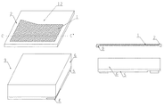
(第1の実施形態)図1の左側は、本発明の第1の実施形態を表す斜視図、右側は点線A−A’の断面図である。発光素子9は、基板6の上に形成された半導体層5と、半導体層5のうちp型層に接続されたp型オーミック電極3と、n型層に接続されたn型オーミック電極4と、p型オーミック電極3からの電流を拡散する目的でp型層表面に形成された補助電極7とを含む。なお、補助電極7は、透明電極をp型層表面に形成することで置き換えてもよい。また、透明電極の上に補助電極7を形成しても良い。 (First Embodiment) The left side of FIG. 1 is a perspective view showing the first embodiment of the present invention, and the right side is a sectional view taken along the dotted line A-A '. The light emitting element 9 includes a semiconductor layer 5 formed on the substrate 6, a p-type ohmic electrode 3 connected to the p-type layer of the semiconductor layer 5, and an n-type ohmic electrode 4 connected to the n-type layer. And an auxiliary electrode 7 formed on the surface of the p-type layer for the purpose of diffusing the current from the p-type ohmic electrode 3. The auxiliary electrode 7 may be replaced by forming a transparent electrode on the p-type layer surface. Further, the auxiliary electrode 7 may be formed on the transparent electrode.
p型オーミック電極3、n型オーミック電極4に対し、通常は、Au線等がワイヤボンドされ、このAu線等によって電源等の外部回路に接続される。Au線等を介して電流が印加されたとき、発光素子9は半導体層5の構成よって定まる波長で発光する。 Usually, an Au wire or the like is wire-bonded to the p-type ohmic electrode 3 and the n-type ohmic electrode 4, and the Au wire or the like is connected to an external circuit such as a power source. When a current is applied via an Au wire or the like, the light emitting element 9 emits light at a wavelength determined by the configuration of the semiconductor layer 5.
発光素子9は、例えばInGaNを発光層として用いた窒化ガリウム系青色発光ダイオードが好適に用いられる。かかる発光ダイオードは、発光層のIn組成に応じて緑色から近紫外の光まで発光波長を変えることができる。従って、光学機能層として蛍光体層を用いる場合、本発明の目的に適した蛍光体の励起波長に応じた、最適の波長を選択すればよい。この場合、窒化ガリウム系発光ダイオード以外には、酸化亜鉛系発光素子、SiC系発光素子、ZnSe系発光素子等も本発明の発光素子として使用しうる。 As the light emitting element 9, for example, a gallium nitride blue light emitting diode using InGaN as a light emitting layer is preferably used. Such a light emitting diode can change the emission wavelength from green to near ultraviolet light according to the In composition of the light emitting layer. Therefore, when a phosphor layer is used as the optical functional layer, an optimum wavelength may be selected according to the excitation wavelength of the phosphor suitable for the purpose of the present invention. In this case, besides the gallium nitride-based light-emitting diode, a zinc oxide-based light-emitting element, a SiC-based light-emitting element, a ZnSe-based light-emitting element, or the like can be used as the light-emitting element of the present invention.
枠部2は、その内側に光学機能層として蛍光体層1を保持している。枠部2下側には、発光素子9の大きさに合わせた段差状の位置合わせ構造8が形成されている。また、枠部2は、ワイヤボンディングを行うための部分であるp型オーミック電極3とn型オーミック電極4の上を覆わないよう、対応する部分を切り欠いた形状としている。蛍光体層1は、蛍光体の組成や濃度によって相違するものの、概ね厚さが10〜700μm程度である。
The frame part 2 holds the
なお、p型オーミック電極3またはn型オーミック電極4のいずれか一方が発光素子9の下面にある場合、対応する部分を切り欠く必要がなくなり、構造がより簡単になる。p型オーミック電極3およびn型オーミック電極4の双方が発光素子9の下面にある、いわゆるフリップチップ型の実装構造をとる場合、枠部2の形状は発光素子9の外形に合わせた正方形ないし長方形とするのみでよい。 When either the p-type ohmic electrode 3 or the n-type ohmic electrode 4 is on the lower surface of the light-emitting element 9, it is not necessary to cut out the corresponding part, and the structure becomes simpler. When a so-called flip chip type mounting structure in which both the p-type ohmic electrode 3 and the n-type ohmic electrode 4 are on the lower surface of the light emitting element 9 is employed, the shape of the frame portion 2 is a square or rectangular shape that matches the outer shape of the light emitting element 9 It is only necessary to do.
枠部2は、発光素子9の上面に、蛍光体層1の位置ずれが起きないように組み合わされる。発光素子に電流が印加され、発光したとき、発光素子9の上面から出る光は、光学機能層1に入射する。蛍光体層1は、この光の一部を吸収し、入射した光の波長とは別の波長の蛍光を発する。この結果、蛍光体層1に入射して変換されなかった発光素子9からの光と、変換された光とで混色光を形成してデバイス外部に放出される。なお、蛍光体層1の構成と発光素子9の構成によっては、蛍光体層1は発光素子9からの発光の、実質的に全てを吸収し、他の波長に変換する。この場合、蛍光体層1からの蛍光のみがデバイス外部に放出される。
The frame portion 2 is combined with the upper surface of the light emitting element 9 so that the
枠部2は、蛍光体層1を保持し、また、発光素子9の上に配置する際の取り扱いがしやすい材料であればよい。特に、発光素子9の大きさが小さい場合には位置合わせ構造8の大きさが小さくなるため、微細な加工がし易い材料が好適である。更に、発光素子9に定格以上の電流を印加して高い発光出力を得たい場合には、発光素子9が発熱する関係上、熱的に変性しにくいものがさらに好適である。このような材料として、ガラス、セラミック、樹脂などが挙げられる。また、シリコン(Si)は、微細加工のし易さと耐熱性を備えるほか、安価でもあるため、好適に使用できる。ガラスまたはシリコンを用いる場合は、ガラス基板またはシリコンウェハに対してフォトリソグラフィ技術によるパターニングと通常のエッチング技術を適用することにより、枠部2の製造が可能である。また、セラミックならば、原材料を開口と位置合わせ構造を縦横に配列させた集合基板の型でプレスし、焼成すればよい。樹脂であれば、通常の成型技術を必要に応じて適用できる。
The frame 2 may be any material that holds the
蛍光体層1は、バインダーとなる樹脂に蛍光体を混合させたものよりなる。発光素子9として青色発光ダイオードを用い、これに黄色蛍光体を組み合わせて白色光を得たい場合、好適にはYAG:Ce、(Sr,Ca,Ba)2SiO4:Eu等が用いられる。また、発光素子として青色発光ダイオードを用い、これに緑色蛍光体と赤色蛍光体を組み合わせて白色光を得たい場合、好適には、緑色蛍光体として(Sr,Ca)Ga2S4:Eu、赤色蛍光体としてCaAlSiN3:Euや(Sr,Ca)S:Eu等が用いられる。
The
バインダーとなる樹脂として、耐熱性と耐光性が求められる。特にシリコーン樹脂がこの要求を満たし、好適に用いられる。シリコーン樹脂の中でも、硬化後も表面タック性を持ちつづける柔軟で粘着性のある樹脂は、発光素子9に蛍光体層1が張り付くため、別体に用意した蛍光体層1と枠部2を発光素子9に配置する際に接着材料を用いる必要がない。従って、かかる工程が簡便で済む利点がある。
As resin used as a binder, heat resistance and light resistance are required. In particular, a silicone resin satisfies this requirement and is preferably used. Among the silicone resins, the soft and sticky resin that continues to have surface tackiness after curing is such that the
枠部2に蛍光体層1を形成するためには、開口を縦横に複数個形成した集合基板を製造し、その開口に蛍光体含有樹脂を充填すればよい。その後、開口を含む枠部をダイシング工程で切り出して個片化することで個別の枠部2が製造できる。
In order to form the
なお、光学機能層として、散乱材を含む散乱層を選択することもできる。特に、発光素子9のような補助電極7を必要とするほど電流の面内拡散が必要となる素子では、素子面内の発光均一性がうまく得られないという問題がある。特に大きさが1mm角ないしそれ以上の半導体発光素子を用いる場合に有効となろう。 A scattering layer containing a scattering material can also be selected as the optical functional layer. In particular, in an element such as the light emitting element 9 that requires in-plane diffusion of current to the extent that the auxiliary electrode 7 is required, there is a problem that light emission uniformity in the element plane cannot be obtained well. This is particularly effective when a semiconductor light emitting device having a size of 1 mm square or more is used.
更に、光学機能層として、表面にマイクロレンズを形成することも出来る。特に、発光素子単体である程度の配光特性を必要とする、小型の電子部品を必要とする分野では有効となろう。 Furthermore, a microlens can be formed on the surface as the optical functional layer. In particular, it will be effective in a field that requires a small electronic component that requires a certain amount of light distribution characteristics with a single light emitting element.
(第2の実施形態)図2の左側は、本発明の第2の実施形態を表す斜視図、右側は点線B−B’の断面図である。なお、同一の部分に対しては同一の番号を付し、本実施形態に特有の特徴以外の説明は以後省略する。 (Second Embodiment) The left side of FIG. 2 is a perspective view showing a second embodiment of the present invention, and the right side is a sectional view taken along the dotted line B-B '. In addition, the same number is attached | subjected to the same part, and description other than the characteristic peculiar to this embodiment is abbreviate | omitted hereafter.
枠部2には、発光素子9と電気的に接続するためのパッド部10a、11a及び枠部2の側面の配線を介して外部回路等と接続するための端子部10c、11cが形成されている。また、発光素子9のp型オーミック電極3の上にパッド部10bが、n型オーミック電極4の上に接続パッド部11bが形成され、枠部2のパッド部10a、11aと対応して形成されている。 The frame portion 2 is formed with pad portions 10a and 11a for electrical connection with the light emitting element 9 and terminal portions 10c and 11c for connection with an external circuit or the like via wiring on the side surface of the frame portion 2. Yes. Further, a pad portion 10 b is formed on the p-type ohmic electrode 3 of the light emitting element 9, and a connection pad portion 11 b is formed on the n-type ohmic electrode 4, corresponding to the pad portions 10 a and 11 a of the frame portion 2. ing.
枠部2を発光素子9上に、位置合わせ構造8を利用して正確に配置することで、パッド部10a、11aは正しく発光素子9のパッド部10b、11bの上に接触して配置されることになる。かかる状態で、電気的接続を確実にするためにパッド部の加熱を行うことで、簡単に枠部2を固定しつつ、端子部10c、11cから外部回路等に接続することができるようになる。 By accurately arranging the frame portion 2 on the light emitting element 9 by using the alignment structure 8, the pad portions 10 a and 11 a are correctly placed in contact with the pad portions 10 b and 11 b of the light emitting element 9. It will be. In this state, the pad portion is heated to ensure electrical connection, so that the frame portion 2 can be easily fixed and the terminal portions 10c and 11c can be connected to an external circuit or the like. .
ここで、枠部2をシリコンで形成した場合、事前にシリコンに対してドーピング等を行っておくなどして、端子部10cと11cの間に静電保護素子としてダイオードやコンデンサを作ることができる。このような構成は、特に静電的に弱い傾向がある窒化ガリウム系半導体発光素子を使用する場合に有用である。 Here, when the frame portion 2 is formed of silicon, a diode or a capacitor can be formed as an electrostatic protection element between the terminal portions 10c and 11c by performing doping or the like on silicon in advance. . Such a configuration is particularly useful when using a gallium nitride based semiconductor light emitting device that tends to be electrostatically weak.
(第3の実施形態)図3の左側は、本発明の第3の実施形態を表す斜視図、右側は点線C−C’の断面図である。図3において、枠部2の開口形状は、遮光部12が形成されているために特有の形状となっている。この開口形状は、車両用前照灯のすれ違い配光を実現するため、カットオフを遮光部12によって形成するものである。遮光部12は、枠部2を製造する際の、例えばフォトリソグラフィ技術を用いる際のパターンをこの形状とするだけで簡単に形成できる。 (Third Embodiment) The left side of FIG. 3 is a perspective view showing a third embodiment of the present invention, and the right side is a sectional view taken along the dotted line C-C '. In FIG. 3, the opening shape of the frame portion 2 is a unique shape because the light shielding portion 12 is formed. This opening shape forms a cut-off by the light-shielding part 12 in order to realize the passing light distribution of the vehicle headlamp. The light-shielding portion 12 can be easily formed by simply forming a pattern when the frame portion 2 is manufactured, for example, when a photolithography technique is used.
なお、実際上、車両用前照灯を本実施形態の発光装置を用いて実現する場合には、カットオフ部分近傍に焦点を持つ投射レンズ(図示せず)を必要とする。 In practice, when a vehicle headlamp is realized using the light emitting device of this embodiment, a projection lens (not shown) having a focal point in the vicinity of the cut-off portion is required.
遮光部12の形状は目的に応じて適切な形状とすることができる。例えば、車両用前照灯のために横長の配光を要求される場合に、開口形状を長方形とするように遮光部12を形成することもできる。また、装飾用の発光装置として、例えば星型の開口形状とすることも自在である。 The shape of the light shielding part 12 can be an appropriate shape according to the purpose. For example, when a horizontally long light distribution is required for a vehicle headlamp, the light shielding portion 12 may be formed so that the opening shape is rectangular. Further, as a decorative light emitting device, for example, a star-shaped opening shape can be freely used.
遮光部12および枠部2の上側表面には、放熱コーティングやアルマイト処理を行って赤外線輻射等を促進し、放熱に役立てても良い。特に、車両用前照灯として本実施形態の発光装置を用いる場合、大電流を印加することとなるため、発光素子9の発熱が非常に多くなる。また、光学機能層1に蛍光体が含まれる場合、蛍光体のストークスシフトによって蛍光体自体も熱を発する。これらを熱を放出する手段の一つとなりうる。
On the upper surface of the light shielding part 12 and the frame part 2, heat radiation coating or anodizing may be performed to promote infrared radiation and the like, which may be useful for heat radiation. In particular, when the light emitting device of the present embodiment is used as a vehicle headlamp, a large current is applied, and thus the light emitting element 9 generates a great amount of heat. When the optical
なお、本実施形態において、遮光部12は枠部2の開口形状を適当な形状として形成したものである。しかし、光学機能層1の表面ないし裏面に適当な形状の遮光膜を形成することで代用しても良い。
In the present embodiment, the light shielding portion 12 is formed by making the opening shape of the frame portion 2 an appropriate shape. However, a light shielding film having an appropriate shape may be formed on the front surface or the back surface of the optical
本実施形態において、発光素子9はいわゆるフリップチップ接合の実装形式をとっている。この場合、枠部2は、発光素子9の基板6の上に位置合わせ構造8によって正確に配置されることとなる。ただし、第2の実施形態のように、p型およびn型オーミック電極が上面側に現れても本発明の効果を損なわない。なお、p型およびn型オーミック電極が上面側ある場合、遮光部12に第2の実施形態にある端子部10c、11c等を形成しても良い。 In the present embodiment, the light emitting element 9 takes a so-called flip chip bonding mounting form. In this case, the frame portion 2 is accurately arranged by the alignment structure 8 on the substrate 6 of the light emitting element 9. However, even if the p-type and n-type ohmic electrodes appear on the upper surface side as in the second embodiment, the effect of the present invention is not impaired. When the p-type and n-type ohmic electrodes are on the upper surface side, the terminal portions 10c, 11c and the like in the second embodiment may be formed in the light shielding portion 12.
以下、本発明の実施例を示す。実施例1では、Si製の枠部を作製した。 Examples of the present invention will be described below. In Example 1, a Si frame portion was produced.
表面が(100)面である単結晶Siウェハ基板(以後、単にSiウェハ基板と呼ぶ)を、正方形の開口形状となるようにフォトリソグラフィによりパターニングした。パターニングは図4に示すものである。その後、Siウェハ基板は、蛍光体含有樹脂を充填する側となる表面をウェットエッチングによって加工された。ウェットエッチングの際、アルカリ系エッチング溶液としてTMAH(Tetramethylammonium hydroxide)を用いた結晶異方性エッチングを行うことで、Siウェハ基板は、枠部内側面に傾斜した(111)面を露出された。この面の傾斜角は、Siウェハ基板の表面に対して54.7°である(開口部側から計測すると125.3°)。 A single crystal Si wafer substrate (hereinafter simply referred to as an Si wafer substrate) having a (100) surface was patterned by photolithography so as to have a square opening shape. The patterning is as shown in FIG. Thereafter, the Si wafer substrate was processed by wet etching on the surface to be filled with the phosphor-containing resin. At the time of wet etching, crystal anisotropic etching using TMAH (Tetramethylammonium Hydroxide) as an alkaline etching solution was performed, whereby the (111) plane inclined to the inner side surface of the frame portion was exposed. The inclination angle of this surface is 54.7 ° with respect to the surface of the Si wafer substrate (125.3 ° when measured from the opening side).
その後、Siウェハ基板は、図4の点線のように裏面に再度パターニングが施され、反応性イオンエッチング(RIE:Reactive Ion Etching)により裏面側から開口部が形成された。ここでは、位置合わせ構造を作製するため、Siウェハ基板の表面側のエッチングパターンより、裏面側からのエッチングパターンの方が大きくなるようにした。Siウェハ基板は、その厚みを300μm、開口形状を表面側が一辺960μmの正方形、裏面側が900μmの正方形とした。ここで、表面側からエッチングする深さと裏面側からエッチングする深さがそれぞれ150μmとして設定したため、Siウェハ基板の厚さ方向の中央で貫通した。 Thereafter, the back surface of the Si wafer substrate was patterned again as indicated by the dotted line in FIG. 4, and an opening was formed from the back surface side by reactive ion etching (RIE). Here, in order to produce the alignment structure, the etching pattern from the back surface side is made larger than the etching pattern from the front surface side of the Si wafer substrate. The Si wafer substrate had a thickness of 300 μm, and the opening shape was a square with a side of 960 μm on the front side and a square with a back side of 900 μm. Here, the depth etched from the front surface side and the depth etched from the back surface side were set to 150 μm, respectively, and therefore penetrated at the center in the thickness direction of the Si wafer substrate.
次に、Si製の枠部による光吸収を防止するため、Si表面には、反射材料としてAg反射膜を電解メッキ法により形成された。 Next, in order to prevent light absorption by the Si frame portion, an Ag reflection film was formed as a reflective material on the Si surface by an electrolytic plating method.
図5は、枠部内にYAG:Ce蛍光体含有樹脂を充填した状態を示したものである。蛍光体含有樹脂の充填は、蛍光体粒子を予め分散させておいたシリコーン樹脂を、枠部開口を用いてスキージですり切ることにより、開口部の深さに応じた一定の膜厚が得られた。その後、樹脂を硬化させ、ダイシングを行って個片化した。ダイシングを行った結果、図6に示す枠部を個片として得ることができた。図6のうち、RIEでエッチングしたことで側面が垂直となった枠部下半分は、発光素子と組み合わされることとなる。一方で、ウェットエッチングによって側面が傾斜した枠部上半分には、YAG:Ce蛍光体含有樹脂が充填される。 FIG. 5 shows a state in which the YAG: Ce phosphor-containing resin is filled in the frame portion. Filling the phosphor-containing resin is achieved by squeezing the silicone resin, in which the phosphor particles are pre-dispersed, with a squeegee using the opening of the frame, to obtain a certain film thickness according to the depth of the opening. It was. Thereafter, the resin was cured and diced into individual pieces. As a result of dicing, the frame shown in FIG. 6 could be obtained as individual pieces. In FIG. 6, the lower half of the frame portion whose side surfaces are vertical due to etching by RIE is combined with the light emitting element. On the other hand, a YAG: Ce phosphor-containing resin is filled in the upper half of the frame portion whose side surfaces are inclined by wet etching.
図7は、フリップチップ実装した発光素子の上に、個片化したSi製の枠部を配置した状態を図示した。枠部は、シリコーン樹脂のタック性を利用してチップ上に配置した。その後、発光素子と枠部を含む全体をシリコーン樹脂で封止することで、発光デバイスを作製できた。 FIG. 7 illustrates a state in which an individual Si frame portion is disposed on a flip-chip mounted light emitting element. The frame was placed on the chip using the tackiness of silicone resin. Then, the light emitting device was able to be manufactured by sealing the whole containing a light emitting element and a frame part with a silicone resin.
1 光学機能層
2 枠部
3 p型オーミック電極
4 n型オーミック電極
5 半導体層
6 基板
7 補助電極
8 位置合わせ構造
9 発光素子
10a パッド部
10b パッド部
10c 端子部
11a パッド部
11b パッド部
11c 端子部
12 遮光部
13 Si(111)面
DESCRIPTION OF
Claims (2)
前記光学機能層外周を囲み、位置合わせ構造を形成された枠部と、
発光素子と、
を含み、
前記発光素子に、前記枠部と前記光学機能層が前記位置合わせ構造によって位置合わせがされた状態で戴置され、
前記枠部は、シリコン(Si)からなると共に前記発光素子との間に電気的接続部が形成され、更に外部電気回路と接続するための外部電気端子が形成され、かつ、静電保護素子としてコンデンサまたはダイオードが形成されていることを特徴とする発光装置。 An optical functional layer;
A frame part that surrounds the outer periphery of the optical functional layer and is formed with an alignment structure;
A light emitting element;
Including
The light emitting element is placed in a state where the frame portion and the optical function layer are aligned by the alignment structure,
The frame portion is made of silicon (Si), and an electrical connection portion is formed between the light emitting device, an external electrical terminal for connection to an external electrical circuit, and an electrostatic protection device. A light-emitting device in which a capacitor or a diode is formed.
前記光学機能層外周を囲み、位置合わせ構造を形成された枠部と、
半導体発光素子と、
を含み、
前記発光素子に、前記枠部と前記光学機能層が前記位置合わせ構造によって位置合わせがされた状態で戴置する発光装置の製造方法であって、
オーミック電極を表面に形成した個片化した前記半導体発光素子を準備する工程と、
ウエハ基板に複数の開口部および前記位置合わせ構造を形成して複数の枠部を一体に形成する工程と、
前記開口部内に、開口部の深さに応じた一定の膜厚の光学機能層を充填し、その後に枠部を個片とする工程
を有する
ことを特徴とする発光装置の製造方法。 An optical functional layer;
A frame part that surrounds the outer periphery of the optical functional layer and is formed with an alignment structure;
A semiconductor light emitting device;
Including
A method of manufacturing a light emitting device in which the light emitting element is placed in a state where the frame portion and the optical functional layer are aligned by the alignment structure,
A step of preparing the semiconductor light emitting element that is separated into pieces with an ohmic electrode formed on the surface;
Forming a plurality of openings and the alignment structure on the wafer substrate to integrally form a plurality of frames;
A method of manufacturing a light-emitting device, comprising: filling the opening with an optical functional layer having a certain thickness according to the depth of the opening, and then dividing the frame into individual pieces.
Priority Applications (1)
| Application Number | Priority Date | Filing Date | Title |
|---|---|---|---|
| JP2007030226A JP5148126B2 (en) | 2007-02-09 | 2007-02-09 | Color conversion light emitting device and manufacturing method thereof |
Applications Claiming Priority (1)
| Application Number | Priority Date | Filing Date | Title |
|---|---|---|---|
| JP2007030226A JP5148126B2 (en) | 2007-02-09 | 2007-02-09 | Color conversion light emitting device and manufacturing method thereof |
Publications (3)
| Publication Number | Publication Date |
|---|---|
| JP2008198702A JP2008198702A (en) | 2008-08-28 |
| JP2008198702A5 JP2008198702A5 (en) | 2010-03-11 |
| JP5148126B2 true JP5148126B2 (en) | 2013-02-20 |
Family
ID=39757401
Family Applications (1)
| Application Number | Title | Priority Date | Filing Date |
|---|---|---|---|
| JP2007030226A Expired - Fee Related JP5148126B2 (en) | 2007-02-09 | 2007-02-09 | Color conversion light emitting device and manufacturing method thereof |
Country Status (1)
| Country | Link |
|---|---|
| JP (1) | JP5148126B2 (en) |
Cited By (1)
| Publication number | Priority date | Publication date | Assignee | Title |
|---|---|---|---|---|
| US11038091B2 (en) | 2019-03-22 | 2021-06-15 | Samsung Electronics Co., Ltd. | Light-emitting device packages |
Families Citing this family (4)
| Publication number | Priority date | Publication date | Assignee | Title |
|---|---|---|---|---|
| JP5146356B2 (en) | 2009-02-24 | 2013-02-20 | 豊田合成株式会社 | Light emitting device and manufacturing method thereof |
| JPWO2011108664A1 (en) * | 2010-03-03 | 2013-06-27 | 有限会社Mtec | Optical semiconductor device |
| JP6387773B2 (en) * | 2014-09-30 | 2018-09-12 | 日亜化学工業株式会社 | Method for manufacturing translucent member and method for manufacturing light emitting device |
| TWI632843B (en) * | 2017-12-01 | 2018-08-11 | 微星科技股份有限公司 | Profile and identity recognizing device |
Family Cites Families (4)
| Publication number | Priority date | Publication date | Assignee | Title |
|---|---|---|---|---|
| JP3149402B2 (en) * | 1999-02-09 | 2001-03-26 | 株式会社ナカニシ | Medical lighting equipment |
| CN101438406B (en) * | 2004-11-19 | 2011-04-20 | 皇家飞利浦电子股份有限公司 | Light-emitting device with inorganic housing |
| JP2006261049A (en) * | 2005-03-18 | 2006-09-28 | Koizumi Sangyo Corp | Multi-point light source unit |
| KR100662844B1 (en) * | 2005-06-10 | 2007-01-02 | 삼성전자주식회사 | Led package structure and manufacturing method, and led array module |
-
2007
- 2007-02-09 JP JP2007030226A patent/JP5148126B2/en not_active Expired - Fee Related
Cited By (1)
| Publication number | Priority date | Publication date | Assignee | Title |
|---|---|---|---|---|
| US11038091B2 (en) | 2019-03-22 | 2021-06-15 | Samsung Electronics Co., Ltd. | Light-emitting device packages |
Also Published As
| Publication number | Publication date |
|---|---|
| JP2008198702A (en) | 2008-08-28 |
Similar Documents
| Publication | Publication Date | Title |
|---|---|---|
| KR102339021B1 (en) | Light emitting device with beveled reflector and manufacturing method of the same | |
| JP6519311B2 (en) | Light emitting device | |
| CN109154425B (en) | Light source device and lighting device | |
| JP5155518B2 (en) | Semiconductor light-emitting device having a prepared wavelength conversion element | |
| JP5526232B2 (en) | Light emitting diode with molded reflective sidewall coating | |
| US8597963B2 (en) | Manufacture of light emitting devices with phosphor wavelength conversion | |
| EP2479812B1 (en) | Semiconductor light emitting device and manufacturing method | |
| US7955879B2 (en) | Method of forming LED semiconductor device having annealed encapsulant layer and annealed luminescence conversion material layer | |
| US8461610B2 (en) | Semiconductor light emitting device having a reflective material with a side slant surface and method of manufacturing | |
| US8581287B2 (en) | Semiconductor light emitting device having a reflective material, wavelength converting layer and optical plate with rough and plane surface regions, and method of manufacturing | |
| EP2642537A2 (en) | Light emitting device and method for manufacturing the same | |
| US20140151734A1 (en) | Light-emitting device and method for manufacturing same | |
| TWI550904B (en) | System and methods providing semiconductor light emitters | |
| JP2008300460A (en) | Optical semiconductor device | |
| JP2010517290A (en) | Wafer level phosphor coating method and apparatus fabricated using the method | |
| JP2013501372A (en) | LED with silicone layer and laminated remote phosphor layer | |
| TW201806190A (en) | Light emitting device and the manufacturing method for same | |
| TW201409767A (en) | Phosphor separated from LED by transparent spacer | |
| JP5148126B2 (en) | Color conversion light emitting device and manufacturing method thereof | |
| JP6936867B2 (en) | Semiconductor modules, display devices, and methods for manufacturing semiconductor modules | |
| US9312457B2 (en) | Light emitting device and method for manufacturing the same | |
| JP2014063832A (en) | Semiconductor light-emitting device and manufacturing method of the same | |
| JP2012009696A (en) | Light emitting device and led illuminating equipment | |
| JP6912743B2 (en) | Light emitting device and its manufacturing method | |
| JP2005142194A (en) | Light emitting diode and its manufacturing method |
Legal Events
| Date | Code | Title | Description |
|---|---|---|---|
| A521 | Written amendment |
Free format text: JAPANESE INTERMEDIATE CODE: A523 Effective date: 20100125 |
|
| A621 | Written request for application examination |
Free format text: JAPANESE INTERMEDIATE CODE: A621 Effective date: 20100125 |
|
| A977 | Report on retrieval |
Free format text: JAPANESE INTERMEDIATE CODE: A971007 Effective date: 20110921 |
|
| A131 | Notification of reasons for refusal |
Free format text: JAPANESE INTERMEDIATE CODE: A131 Effective date: 20111011 |
|
| A521 | Written amendment |
Free format text: JAPANESE INTERMEDIATE CODE: A523 Effective date: 20111208 |
|
| A131 | Notification of reasons for refusal |
Free format text: JAPANESE INTERMEDIATE CODE: A131 Effective date: 20120313 |
|
| A521 | Written amendment |
Free format text: JAPANESE INTERMEDIATE CODE: A523 Effective date: 20120416 |
|
| TRDD | Decision of grant or rejection written | ||
| A01 | Written decision to grant a patent or to grant a registration (utility model) |
Free format text: JAPANESE INTERMEDIATE CODE: A01 Effective date: 20121120 |
|
| A61 | First payment of annual fees (during grant procedure) |
Free format text: JAPANESE INTERMEDIATE CODE: A61 Effective date: 20121128 |
|
| R150 | Certificate of patent or registration of utility model |
Ref document number: 5148126 Country of ref document: JP Free format text: JAPANESE INTERMEDIATE CODE: R150 Free format text: JAPANESE INTERMEDIATE CODE: R150 |
|
| FPAY | Renewal fee payment (event date is renewal date of database) |
Free format text: PAYMENT UNTIL: 20151207 Year of fee payment: 3 |
|
| R250 | Receipt of annual fees |
Free format text: JAPANESE INTERMEDIATE CODE: R250 |
|
| R250 | Receipt of annual fees |
Free format text: JAPANESE INTERMEDIATE CODE: R250 |
|
| R250 | Receipt of annual fees |
Free format text: JAPANESE INTERMEDIATE CODE: R250 |
|
| R250 | Receipt of annual fees |
Free format text: JAPANESE INTERMEDIATE CODE: R250 |
|
| R250 | Receipt of annual fees |
Free format text: JAPANESE INTERMEDIATE CODE: R250 |
|
| LAPS | Cancellation because of no payment of annual fees |