JP5144192B2 - Group III nitride crystal growth method - Google Patents
Group III nitride crystal growth method Download PDFInfo
- Publication number
- JP5144192B2 JP5144192B2 JP2007245838A JP2007245838A JP5144192B2 JP 5144192 B2 JP5144192 B2 JP 5144192B2 JP 2007245838 A JP2007245838 A JP 2007245838A JP 2007245838 A JP2007245838 A JP 2007245838A JP 5144192 B2 JP5144192 B2 JP 5144192B2
- Authority
- JP
- Japan
- Prior art keywords
- group iii
- iii nitride
- nitride crystal
- crystal
- main surface
- Prior art date
- Legal status (The legal status is an assumption and is not a legal conclusion. Google has not performed a legal analysis and makes no representation as to the accuracy of the status listed.)
- Expired - Fee Related
Links
Images

Landscapes
- Crystals, And After-Treatments Of Crystals (AREA)
Description
本発明は、発光素子、電子素子、半導体センサなどの各種半導体デバイスの基板として好ましく用いられる転位密度が低いIII族窒化物結晶の成長方法に関する。 The present invention relates to a method for growing a group III nitride crystal having a low dislocation density, which is preferably used as a substrate for various semiconductor devices such as light-emitting elements, electronic elements, and semiconductor sensors.
AlxGayIn1-x-yN結晶(0≦x、0≦y、x+y≦1、以下同じ)などのIII族窒化物結晶は、発光素子、電子素子、半導体センサなどの各種半導体デバイスの基板を形成するための材料として非常に有用なものである。ここで、各種半導体デバイスの特性を向上させるために、転位密度が低く結晶性のよいIII族窒化物結晶が必要とされている。 Group III nitride crystals such as Al x Ga y In 1-xy N crystal (0 ≦ x, 0 ≦ y, x + y ≦ 1, and so on) are substrates for various semiconductor devices such as light emitting elements, electronic elements, and semiconductor sensors. It is very useful as a material for forming. Here, in order to improve the characteristics of various semiconductor devices, a group III nitride crystal having a low dislocation density and good crystallinity is required.
かかるIII族窒化物結晶を成長させる方法として、超高温超高圧溶液法、フラックス法などの液相法、HVPE(ハイドライド気相成長)法、MOCVD(有機金属化学気相堆積)法などの気相法が提案されている。 As a method of growing such a group III nitride crystal, a liquid phase method such as an ultrahigh temperature ultrahigh pressure solution method, a flux method, a gas phase such as an HVPE (hydride vapor phase epitaxy) method, and a MOCVD (metal organic chemical vapor deposition) method. A law has been proposed.
たとえば、特開2004−244307号公報(以下、特許文献1という)は、基板と、その基板上に形成された半導体層と、その半導体層の上方に形成されたIII族窒化物結晶とを備えるIII族窒化物基板であって、上記半導体層が、組成式AluGavIn1-u-vN(0≦u≦1、0≦v≦1)で表される半導体からなり、その半導体層の表面が(0001)面のステップが階段状に配置された一方向に傾斜した面であり、その傾斜した面と上記(0001)面とのなす角が、0.05°以上であり、さらに、上記半導体層上に形成されたIII族窒化物結晶のキャリア濃度の面内ばらつきが、キャリア濃度の平均値の1/5以上5倍以下であるIII族窒化物基板を開示する。 For example, Japanese Unexamined Patent Application Publication No. 2004-244307 (hereinafter referred to as Patent Document 1) includes a substrate, a semiconductor layer formed on the substrate, and a group III nitride crystal formed above the semiconductor layer. A group III nitride substrate, wherein the semiconductor layer is made of a semiconductor represented by a composition formula Al u Ga v In 1-uv N (0 ≦ u ≦ 1, 0 ≦ v ≦ 1), The surface is a (0001) plane step inclined in one direction arranged stepwise, the angle between the inclined plane and the (0001) plane is 0.05 ° or more, and A group III nitride substrate is disclosed in which the in-plane variation of the carrier concentration of the group III nitride crystal formed on the semiconductor layer is 1/5 or more and 5 times or less of the average value of the carrier concentration.
ここで、上記特許文献1は、かかるIII族窒化物結晶基板の製造方法として、基板上に、組成式AluGavIn1-u-vN(0≦u≦1、0≦v≦1)で表される半導体であって、その表面に(0001)面が存在する半導体層を形成する工程と、その半導体層の(0001)面に対して傾斜した面となるように半導体層の表面を処理する工程と、窒素を含む雰囲気下において、Ga(ガリウム)、Al(アルミニウム)およびIn(インジウム)から選ばれる少なくとも1つのIII族元素と溶剤とを含む融液に、その半導体層の表面を接触させることによって、少なくとも1つのIII族元素と窒素とを反応させて上記半導体層上にIII族窒化物結晶を成長させる工程とを含む。
Here, in
上記特許文献1の方法においては、半導体層の表面が、(0001)面が露出した階段状に加工されている。そのため、結晶育成時の異常成長を防止できる。また通常の種結晶基板を用いた場合と比較して、表面平坦性が高い結晶を得ることができる。特に、液相成長において、傾斜した基板を用いることにより、傾斜した基板を用いない場合に比べて、成長速度の向上と結晶中に取り込まれる不純物濃度の均一性が向上することが可能となる。
In the method of
ここで、主面が(0001)面であるIII族窒化物基板上にIII族窒化物結晶を成長させた場合、III族窒化物基板の転位がIII族窒化物結晶の成長方向である[0001]方向に伝搬しIII族窒化物結晶の成長表面に到達する。III族窒化物結晶を厚く成長させると、バーガーズベクトルの符号が反対で大きさが同じ転位同士が引力により合体して消滅することにより、III族窒化物結晶の転位密度が低減する。 Here, when a group III nitride crystal is grown on a group III nitride substrate whose principal surface is the (0001) plane, the dislocation of the group III nitride substrate is the growth direction of the group III nitride crystal [0001] ] To the growth surface of the group III nitride crystal. When a group III nitride crystal is grown thickly, dislocations having the same sign of the Burgers vector but having the same magnitude merge by attraction and disappear, thereby reducing the dislocation density of the group III nitride crystal.
しかし、結晶の転位密度が1×107cm-2未満になると、転位間の間隔が大きくなるため上記のような転位の合体が生じる可能性が極めて低くなる。すなわち、転位密度が1×107cm-2未満のIII族窒化物結晶基板にIII族窒化物結晶を成長させる場合、下地基板であるIII族窒化物結晶基板に比べて転位密度が低いIII族窒化物結晶を成長させることは困難であった。 However, when the dislocation density of the crystal is less than 1 × 10 7 cm −2 , the distance between the dislocations is increased, so that the possibility of the above-described dislocation coalescence is extremely reduced. That is, when a group III nitride crystal is grown on a group III nitride crystal substrate having a dislocation density of less than 1 × 10 7 cm −2 , the group III has a lower dislocation density than the group III nitride crystal substrate that is the base substrate. It was difficult to grow nitride crystals.
また、従来のIII族窒化物結晶は、通常、下地基板であるIII族窒化物結晶基板の主面である(0001)面上にエピタキシャル成長させて得られるものであることから、その結晶成長面も(0001)面となり、(0001)面がその結晶の主面となる。かかる(0001)面は、その面の垂直方向に極性を有する極性面である。このため、III族窒化物結晶の主面である(0001)面上に少なくとも1層の半導体結晶層を形成して得られる半導体デバイスは、分解電界が発生して電子と正孔が空間的に分離するため、発光効率などのデバイス特性が低下する問題点があった。このため、その面の垂直方向に極性がない非極性面を主面とする結晶が望まれていた。
本発明は、非極性面を主面とする転位密度が低いIII族窒化物結晶の成長方法を提供することを目的とする。 An object of the present invention is to provide a method for growing a group III nitride crystal having a nonpolar plane as a main surface and a low dislocation density.
本発明は、下地基板を準備する工程を備え、下地基板は、一主面を有するIII族窒化物種結晶を含み、その主面がIII族窒化物結晶の{1−100}面に対して0.1°以上10°以下の傾き角を有し、かつその主面における転位密度が1×10 7 cm -2 未満であって、下地基板の主面にIII族金属とアルカリ金属を含む溶媒に窒素含有ガスを溶解させた溶液を接触させて、下地基板の主面上に第1のIII族窒化物結晶をエピタキシャル成長させる工程をさらに備え、第1のIII族窒化物結晶の成長後の結晶成長面における転位密度が下地基板の上記主面における転位密度の1/10以下であるIII族窒化物結晶の成長方法である。 The present invention includes a step of preparing a base substrate, the base substrate is seen containing a group III nitride seed crystal having a principal surface, with respect to {1-100} plane of the main surface III nitride crystal A solvent having a tilt angle of 0.1 ° or more and 10 ° or less and having a dislocation density of less than 1 × 10 7 cm −2 on the main surface thereof and containing a group III metal and an alkali metal on the main surface of the base substrate to contacting the solution of a nitrogen-containing gas, the base substrate first further example Bei group III step of nitride crystal epitaxially grown on the main surface of the first group-III nitride crystal after growth the dislocation density in the crystal growth surface is a growth method of 1/10 der Ru III nitride crystal of dislocation density in the main surface of the base substrate.
本発明にかかるIII族窒化物結晶の成長方法において、第1のIII族窒化物結晶のエピタキシャル成長の際に、第1のIII族窒化物結晶に存在する転位の少なくとも一部が、III族窒化物結晶の{1−100}面に対して実質的に平行な方向に伝搬して、第1のIII族窒化物結晶の外周部に排出され得る。 In the method for growing a group III nitride crystal according to the present invention, at the time of epitaxial growth of the first group III nitride crystal, at least a part of dislocations present in the first group III nitride crystal is a group III nitride. It propagates in a direction substantially parallel to the {1-100} plane of the crystal and can be discharged to the outer periphery of the first group III nitride crystal .
また、本発明にかかるIII族窒化物結晶の成長方法において、上記の成長方法により得られた第1のIII族窒化物結晶に主面を形成する工程をさらに備え、第1のIII族窒化物結晶の主面はIII族窒化物結晶の{1−100}面に対して0.1°以上10°以下の傾き角を有し、第1のIII族窒化物結晶の主面にIII族金属とアルカリ金属を含む溶媒に窒素含有ガスを溶解させた溶液を接触させて、第1のIII族窒化物結晶の主面上に第2のIII族窒化物結晶をエピタキシャル成長させる工程をさらに備えることができる。 The method for growing a group III nitride crystal according to the present invention further comprises a step of forming a main surface on the first group III nitride crystal obtained by the above growth method. The main surface of the crystal has an inclination angle of 0.1 ° to 10 ° with respect to the {1-100} plane of the group III nitride crystal, and the group III metal is formed on the main surface of the first group III nitride crystal. And a step in which a solution containing a nitrogen-containing gas dissolved in a solvent containing alkali metal is contacted to epitaxially grow a second group III nitride crystal on the main surface of the first group III nitride crystal. it can.
ここで、第2のIII族窒化物結晶のエピタキシャル成長の際に、第2のIII族窒化物結晶に存在する転位の少なくとも一部が、III族窒化物結晶の{1−100}面に対して実質的に平行な方向に伝搬して、第2のIII族窒化物結晶の外周部に排出され得る。また、下地基板の主面の傾き方向と第1のIII族窒化物結晶の主面の傾き方向とのなす角を、80°以上100°以下とすることができる。また、下地基板の主面における転位密度が1×107cm-2未満であって、第2のIII族窒化物結晶の成長後の結晶成長面における転位密度を下地基板の主面における転位密度の1/100以下とすることができる。 Here, at the time of epitaxial growth of the second group III nitride crystal, at least a part of the dislocations existing in the second group III nitride crystal is relative to the {1-100} plane of the group III nitride crystal. Propagating in a substantially parallel direction and discharged to the outer periphery of the second group III nitride crystal. Further, the angle formed by the tilt direction of the main surface of the base substrate and the tilt direction of the main surface of the first group III nitride crystal can be set to 80 ° or more and 100 ° or less. Further, the dislocation density on the main surface of the base substrate is less than 1 × 10 7 cm −2 , and the dislocation density on the crystal growth surface after the growth of the second group III nitride crystal is expressed as the dislocation density on the main surface of the base substrate. 1/100 or less.
また、本発明にかかるIII族窒化物結晶の成長方法において、アルカリ金属を、NaおよびLiの少なくともいずれかの金属とすることができる。 In the method for growing a group III nitride crystal according to the present invention, the alkali metal can be at least one of Na and Li.
また、本発明にかかるIII族窒化物結晶の成長方法において、上記のいずれかの成長方法により得られた第1のIII族窒化物結晶に主面を形成する工程と、第1のIII族窒化物結晶の主面上に第3のIII族窒化物結晶をエピタキシャル成長させる工程とさらに含むことができる。また、上記のいずれかの成長方法により得られた第2のIII族窒化物結晶に主面を形成する工程と、第2のIII族窒化物結晶の主面上に第4のIII族窒化物結晶をエピタキシャル成長させる工程とをさらに含むことができる。 Moreover, in the method for growing a group III nitride crystal according to the present invention, a step of forming a main surface on the first group III nitride crystal obtained by any one of the above growth methods, and a first group III nitride And epitaxially growing a third group III nitride crystal on the main surface of the physical crystal. A step of forming a main surface on the second group III nitride crystal obtained by any one of the above growth methods; and a fourth group III nitride on the main surface of the second group III nitride crystal. And a step of epitaxially growing the crystal.
本発明によれば、非極性面を主面とする転位密度が低いIII族窒化物結晶の成長方法を提供することができる。 ADVANTAGE OF THE INVENTION According to this invention, the growth method of a group III nitride crystal with a low dislocation density which makes a nonpolar surface a main surface can be provided.
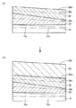
(実施形態1)
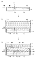
本発明にかかるIII族窒化物結晶の成長方法の一実施形態は、図1を参照して、下地基板10を準備する工程(図1(a))を備える。ここで、下地基板10は一主面10mを有するIII族窒化物種結晶10aを含みかつ主面10mがIII族窒化物結晶の{1−100}面10cに対して0.1°以上10°以下の傾き角を有する。また、下地基板10の主面10mにIII族金属元素とアルカリ金属元素を含む溶媒3に窒素含有ガス5を溶解させた溶液を接触させて(図1(b))、下地基板10の主面10m上に第1のIII族窒化物結晶20をエピタキシャル成長させる工程(図1(c))をさらに備える。
(Embodiment 1)
One embodiment of a method for growing a group III nitride crystal according to the present invention includes a step of preparing a base substrate 10 (FIG. 1A) with reference to FIG. Here,
本実施形態のIII族窒化物結晶の成長方法によれば、第1のIII族窒化物結晶20のエピタキシャル成長の際に、第1のIII族窒化物結晶20に存在する転位の少なくとも一部が、III族窒化物結晶の{1−100}面10cに対して実質的に平行な方向に伝搬して、第1のIII族窒化物結晶20の外周部に排出される。これにより、第1のIII族窒化物結晶20の転位密度を低減することができる。
According to the group III nitride crystal growth method of the present embodiment, at the time of epitaxial growth of the first group III
本実施形態のIII族窒化物結晶の成長方法は、図1(a)を参照して、下地基板10を準備する工程(下地基板準備工程)を備える。準備される下地基板10は、一主面10mを有するIII族窒化物種結晶10aを含みかつ主面10mがIII族窒化物結晶の{1−100}面10cに対して0.1°以上10°以下の傾き角を有する。下地基板10は、一主面10mを有するIII族窒化物種結晶10aを含むため、その主面10m上に第1のIII族窒化物結晶10をエピタキシャル成長させることが可能となる。したがって、下地基板10のIII族窒化物結晶の{1−100}面10cに対して傾き角θ1が0.1°以上10°以下、すなわち、{1−100}面10cに近い面方位を有する主面10m上に第1のIII族窒化物結晶20がエピタキシャル成長する。
The group III nitride crystal growth method of this embodiment includes a step of preparing the base substrate 10 (base substrate preparation step) with reference to FIG. The prepared
上記エピタキシャル成長において、第1のIII族窒化物結晶20は、下地基板10のIII族窒化物種結晶10aの面方位を受け継ぐため、III族窒化物種結晶10の{1−100}面10cおよび第1のIII族窒化物結晶20の{1−100}面20cは、いずれもIII族窒化物結晶の{1−100}面10c、20cとして、互いに平行な面である。したがって、第1のIII族窒化物結晶の結晶成長面20sは{1−100}面である。これにより、非極性面たる{1−100}面である結晶成長面20mを有する第1のIII族窒化物結晶20が得られる。
In the epitaxial growth, since the first group III
ここで、下地基板10は、主面10mを有するIII族窒化物種結晶10aを含むものであれば特に制限はなく、下地基板10全体がIII族窒化物種結晶10aであってもよく、下地基板10がIII族窒化物種結晶10aとそれ以外のものを含むもの、たとえばIII族窒化物種結晶10aがIII族窒化物以外の異種基板上に形成されているテンプレート基板であってもよい。
Here, the
また、エピタキシャル成長させる第1のIII族窒化物結晶20は、特に制限はないが、基板10のIII族窒化物種結晶10aとの間の格子整合性を高めるため、III族窒化物種結晶10aと同じ化学組成を有することが好ましい。
The first group
ここで、上記のような下地基板10の製造方法は、特に制限はなく、たとえば以下の方法が可能である。すなわち、従来の通常の気相法または液相法で、主面を(0001)面とするIII族窒化物バルク結晶を厚く成長させる。得られたIII族窒化物バルク結晶を、III族窒化物結晶の{1−100}面に対して0.5°以上10°以下の傾き角を有する面に平行な面でスライスして、スライス面を研磨および/または研削することにより鏡面化することにより得られる。スライス方法には、特に制限はなく、ワイヤソー、内周刃、外周刃、レーザ光などが用いられる。
Here, the manufacturing method of the
また、下地基板10の主面10mがIII族窒化物結晶の{1−100}面10cに対して0.1°以上10°以下の傾き角θ1を有しているため、第1のIII族窒化物結晶20の成長の際、第1のIII族窒化物結晶20に存在する転位の少なくとも一部が、{1−100}面10cに対して実質的に平行な方向に伝搬して、第1のIII族窒化物結晶の外周部に排出される。
Further, since the
また、本実施形態のIII族窒化物結晶の成長方法は、図1(b)および(c)を参照して、上記下地基板10の主面10mにIII族金属とアルカリ金属を含む溶媒3に窒素含有ガス5を溶解させた溶液を接触させて、下地基板10の主面10m上に第1のIII族窒化物結晶20をエピタキシャル成長させる工程(第1のIII族窒化物結晶成長工程)をさらに備える。かかる第1のIII族窒化物結晶20のエピタキシャル成長工程は、たとえば、以下のようにして行なわれる。
Further, in the method for growing a group III nitride crystal of this embodiment, referring to FIGS. 1B and 1C, a solvent 3 containing a group III metal and an alkali metal on the
まず、図1(b)を参照して、結晶成長容器1内に、下地基板1をその主面1mを上に向けて配置し、III族金属とアルカリ金属を含む溶媒3を入れる。この溶媒3は室温(約25℃)中では固体であるが、後の加熱によって液化する。
First, referring to FIG. 1B, a
III族金属とアルカリ金属を含む溶媒3には、特に制限はないが、純度の高いIII族窒化物結晶10を成長させる観点から、III族金属およびアルカリ金属の純度の高いものが好ましい。かかる観点から、溶媒3は、純度が99モル%以上のIII族金属と純度が99モル%以上のアルカリ金属の混合物が好ましく、99.999モル%以上のIII族金属と99.999モル%以上のアルカリ金属の混合物がより好ましい。ここで、溶媒3が2種類以上のIII族金属を含む場合は、各種III族金属のそれぞれの純度が、99モル%以上であることが好ましく、99.999モル%以上であることがより好ましい。また、溶媒3が2種類以上のアルカリ金属を含む場合は、各種アルカリ金属のそれぞれの純度が、99モル%以上であることが好ましく、99.999モル%以上であることがより好ましい。
Although there is no restriction | limiting in particular in the solvent 3 containing a III group metal and an alkali metal, From the viewpoint of growing the high purity group III nitride crystal |
III族金属およびアルカリ金属を含む溶媒3を用いると、III族金属を含み不純物濃度(たとえば溶媒全体に対して1モル%未満の濃度)以上にはアルカリ金属を含まない溶媒を用いる場合に比べて、III族窒化物結晶の成長温度、成長圧力を低減させ、結晶成長速度を高めることができる。これは、溶媒3に含まれているアルカリ金属が、溶媒3への窒素含有物5の溶解を促進させるためと考えられる。ここで、アルカリ金属は、特に制限はないが、III族窒化物結晶の成長を促進させる観点から、NaおよびLiの少なくともいずれかの金属であることが好ましい。
When the solvent 3 containing a Group III metal and an alkali metal is used, the concentration of impurities including the Group III metal (for example, a concentration of less than 1 mol% with respect to the whole solvent) or higher is used compared to the case of using a solvent containing no alkali metal It is possible to reduce the growth temperature and pressure of the group III nitride crystal and increase the crystal growth rate. This is presumably because the alkali metal contained in the solvent 3 promotes the dissolution of the nitrogen-containing
溶媒3に含まれるIII族金属原子MIIIとアルカリ金属原子MAとのモル比は、特に制限はないが、III族窒化物結晶の成長温度、成長圧力を低減させ、結晶成長速度を高める観点から、MIII:MA=90:10〜10:90が好ましく、MIII:MA=50:50〜20:80がより好ましい。MIII:MA=90:10よりIII族金属原子MIIIのモル比が大きくても、MIII:MA=10:90よりアルカリ金属原子MAのモル比が大きくても、結晶成長速度が低下する。 The molar ratio of the group III metal atom M III and the alkali metal atom M A contained in the solvent 3 is not particularly limited, but the viewpoint of increasing the crystal growth rate by reducing the growth temperature and pressure of the group III nitride crystal. Therefore, M III : M A = 90: 10 to 10:90 is preferable, and M III : M A = 50: 50 to 20:80 is more preferable. Even if the molar ratio of group III metal atom M III is larger than M III : M A = 90: 10, and the molar ratio of alkali metal atom M A is larger than M III : M A = 10: 90, the crystal growth rate Decreases.
また、結晶成長容器1に入れられるIII族金属およびアルカリ金属を含む溶媒3の量は、特に制限はないが、液化した溶媒3(融液)の深さは、溶媒3の表面から下地基板10の主面10mまでが、1mm以上50mm以下であることが好ましい。かかる深さが1mmより小さいと溶媒3の表面張力のため下地基板10の主面10mを溶媒3(融液)が覆わない恐れがあり、50mmより大きいと溶媒3の液面からの窒素の供給が不足してしまうためである。
Further, the amount of the solvent 3 containing a group III metal and an alkali metal put in the
次に、下地基板10と、III族金属およびアルカリ金属を含む溶媒3とが配置された結晶成長容器1を加熱し、結晶成長容器1内の溶媒3内に窒素含有ガス5を供給して、結晶成長容器1内の温度(結晶成長温度)を700℃〜900℃結晶成長容器1内の窒素含有ガスの圧力(結晶成長圧力)を0.5MPa〜5MPaとする。このとき、III族金属とアルカリ金属を含む溶媒3が液化して、液化した溶媒3中に窒素含有ガス5が溶解する。このようにして、III族金属を含む溶媒3に窒素含有ガス5が溶解した溶液を下地基板10の主面10mに接触させることができ、主面10m上に第1のIII族窒化物結晶20がエピタキシャル成長する。
Next, the
かかる下地基板10の主面10m上にIII族窒化物結晶20をエピタキシャル成長させると、下地基板10から受け継がれ、または、結晶成長の際に発生し、III族窒化物結晶20に存在する転位の少なくとも一部が{1−100}面10c,20cに対して実質的に平行な方向に伝搬してIII族窒化物結晶20の外周部に排出されるため、第1のIII族窒化物結晶20の転位密度を低減することができる。
When the group
このような低減方法は、バーガーズベクトルの符号が反対で大きさが同じ転位同士が引力により合体して消滅することによる転位密度の低減とは異なり、結晶の転位密度が1×107cm-2未満となっても、転位密度をさらに低減することができる。結晶の表面における転位密度は、カソードルミネッセンス(CL)法により測定することができる。 Such a reduction method is different from the reduction in dislocation density in which dislocations having the same sign of the Burgers vector but having the same magnitude are merged together by attraction and disappear, and the dislocation density of the crystal is 1 × 10 7 cm −2. Even if it is less than this, the dislocation density can be further reduced. The dislocation density at the surface of the crystal can be measured by a cathodoluminescence (CL) method.
ここで、結晶の{hkil}面、<hkil>方向は、結晶のX線回折により特定することができる。ここで、i=−(h+k)であり、h、kおよびlは、いずれも整数であり、それぞれ同じであっても異なっていてもよい。また、結晶の転位の伝搬の様子(転位伝搬線20d)は、光散乱トモグラフ法により観察することができる。なお、{hkil}面とは、(hkil)面および(hkil)面と幾何学的に等価な結晶面を含む総称である。<hkil>方向とは、[hkil]方向および[hkil]方向と幾何学的に等価な方向を含む総称である。
Here, the {hkil} plane and the <hkil> direction of the crystal can be specified by X-ray diffraction of the crystal. Here, i = − (h + k), and h, k, and l are all integers, and may be the same or different. The state of dislocation propagation (
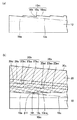
本実施形態における第1のIII族窒化物結晶20の転位の低減のメカニズムを以下に説明する。図2(a)を参照して、本実施形態における下地基板10の主面10mは、ミクロ的には、複数の{1−100}面である複数のテラス面10mcと、それらのテラス面10mcそれぞれに対してそれぞれがある角度を持つ複数のステップ面10tとで、それぞれ構成される複数のステップ10sを有する階段状の凹凸面である。
A mechanism for reducing dislocations in the first group
図2(b)を参照して、上記のような主面10m上に第1のIII族窒化物結晶20を成長させると、第1のIII族窒化物結晶20は、主面10mのテラス面10mcからこのテラス面10mcに垂直な方向と、主面10mのステップ面10tからテラス面10mcに平行な方向に成長する。このため、第1のIII族窒化物結晶20の成長中の結晶成長面20a,20bには、複数の{1−100}面である複数のテラス面20ac,20bcと、それらのテラス面20ac,20bcのそれぞれに対してそれぞれがある角度を有する複数のステップ面20at,20btとで、それぞれ構成される複数のステップ20as,20bsが形成される。
Referring to FIG. 2B, when the first group
ここで、テラス面20ac,20bcに平行な方向の結晶成長は、テラス面20ac,20bcに垂直な方向の結晶成長に比べて優勢である。また、転位は結晶の成長方向に伝搬する。このため、下地基板10の主面から受け継がれ、または、結晶成長の際に発生して、結晶に存在する転位を{1−100}方向に実質的に平行に伝搬させて(図1(c)および図2(b)の転位伝搬線20dを参照)、結晶の外周部に排出させることができるものと考えられる。ここで、転位伝搬線20dとは、転位の伝搬の軌跡を示す線をいう。
Here, crystal growth in a direction parallel to the terrace surfaces 20ac and 20bc is superior to crystal growth in a direction perpendicular to the terrace surfaces 20ac and 20bc. Dislocations propagate in the crystal growth direction. For this reason, it is inherited from the main surface of the
ここで、結晶に存在する転位が伝搬する方向である{1−100}面に実質的に平行な方向とは、フラックス法による第1のIII族窒化物結晶20の成長において、テラス面20ac,20bcに平行な方向の結晶成長速度はテラス面20ac,20bcに垂直な方向の結晶成長速度に比べて約2倍以上となることから、テラス面20ac,20bcに対する傾き角φ1(これは、転位伝搬線20dと{1−100}面10c,20cとのなす転位伝搬角φ1でもある)が約26°以下の方向を意味する。
Here, the direction substantially parallel to the {1-100} plane, which is the direction in which dislocations existing in the crystal propagate, is the terrace plane 20ac, in the growth of the first group
図2(b)を参照して、III族窒化物結晶20の成長とともに、ステップ面20at,20btが転位とともに結晶の外周部へ移動(ステップ・フロー)して、ある結晶成長面20eにおいてステップ面が消滅する。さらに、結晶が{1−100}面20cに垂直な方向に成長して結晶成長面20sとして{1−100}面を有する第1のIII族窒化物結晶20が得られる。このようにして、{1−100}面という非極性面である結晶成長面20sにおける転位密度が低減した第1のIII族窒化物結晶20が得られる。
Referring to FIG. 2B, as the group
下地基板10において、III族窒化物結晶の{1−100}面10cに対する主面10mの傾き角θ1が、0.1°より小さいと下地基板10の主面10mに存在するステップ10sの数が少なく転位を{1−100}面と実質的に平行な方向に効率的に伝搬させることができなくなり、10°より大きいと主面10mに存在するステップ10sの数が多くなり、結晶成長中にステップ20as,20bsが合体してマクロステップ化する(図示せず)。マクロステップが生じると、マクロステップに溶媒3が巻き込まれて結晶中に液胞が生じやすくなる。かかる観点から、傾き角θ1は、0.1°以上10°以下であることがより好ましい。
In the
また、{1−100}面10cに対する主面10mの傾きの方向10hは、特に制限はないが、結晶対称性の観点から、<0001>方向、<11−20>方向などであることが好ましく、<0001>方向がより好ましい。ここで、<0001>方向には、幾何学的に等価な[0001]方向((0001)Ga面の法線方向)と[000−1]方向((000−1)N面の法線方向)が存在する。本実施形態においては、下地基板10の主面10mの傾き方向10hが、[0001]方向および[000−1]方向のいずれの方向であっても、第1のIII族窒化物結晶20の結晶成長面にステップの形成が可能である。下地基板10の主面の傾き方向10hは、ステップ・フローの速度が高い観点から、[0001]方向であることがより好ましい。
Further, the
本実施形態のIII族窒化物結晶の成長方法においては、上記の傾き角θ1に加えて、主面10mにおける転位密度が1×107cm-2未満の下地基板10の主面10m上に成長させる第1のIII族窒化物結晶20の成長後の結晶成長面20sにおける転位密度が下地基板10の主面10mにおける転位密度の1/10以下とすることができる。
In the group III nitride crystal growth method of this embodiment, in addition to the tilt angle θ1, the growth is performed on the
本実施形態においては、バーガーズベクトルの符号が反対で大きさが同じ転位同士が引力により合体して消滅することによる転位密度の低減とは異なり、第1のIII族窒化物結晶20に存在する転位の少なくとも一部を{1−100}面10c、20cに実質的に平行な方向に伝搬させて結晶の外周部に排出させて転位密度の低減を図っているため、下地基板10の主面10mにおける転位密度が1×107cm-2未満であっても、成長させる第1のIII族窒化物結晶20の転位密度をさらに低減させ、成長後の結晶成長面20sにおける転位密度を下地基板10の主面10mにおける転位密度の1/10以下とすることができる。
In the present embodiment, dislocations present in the first group
(実施形態2)
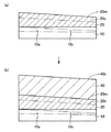
本発明にかかるIII族窒化物結晶の成長方法の他の実施形態は、図3を参照して、実施形態1の成長方法により得られた第1のIII族窒化物結晶20に主面20mを形成する工程(図3(a))をさらに備える。ここで、第1のIII族窒化物結晶20の主面20mは、{1−100}面10c,20cに対して0.1°以上10°以下の傾き角θ2を有する。また、第1のIII族窒化物結晶20の主面20mにIII族金属とアルカリ金属を含む溶媒3に窒素含有ガス5を溶解させた溶液を接触させて(図3(b))、第1のIII族窒化物結晶20の主面20m上に第2のIII族窒化物結晶30をエピタキシャル成長させる工程(図3(c))をさらに備える。
(Embodiment 2)
In another embodiment of the group III nitride crystal growth method according to the present invention, referring to FIG. 3, a
本実施形態のIII族窒化物結晶の成長方法によれば、第2のIII族窒化物結晶30のエピタキシャル成長の際に、第2のIII族窒化物結晶30に存在する転位の少なくとも一部が、III族窒化物結晶の{1−100}面10c,20c,30cに対して実質的に平行な方向に伝搬して、第2のIII族窒化物結晶20の外周部に排出される。これにより、第2のIII族窒化物結晶30の転位密度を低減することができる。
According to the Group III nitride crystal growth method of the present embodiment, at the time of epitaxial growth of the second Group
本実施形態のIII族窒化物結晶の成長方法は、図3(a)を参照して、実施形態1の成長方法により得られた第1のIII族窒化物結晶20に主面20mを形成する工程をさらに備える。かかる工程において、主面20mの形成方法には、特に制限はなく、切断、切削、研磨など各種の方法が可能である。
The growth method of the group III nitride crystal of this embodiment forms a
第1のIII族窒化物結晶20の主面20mは、III族窒化物結晶の{1−100}面10c,20cに対して0.1°以上10°以下の傾き角θ2を有しているため、第2のIII族窒化物結晶30の成長の際、第2のIII族窒化物結晶30に存在する転位の少なくとも一部が、{1−100}面10c,20cに対して実質的に平行な方向に伝搬して、第2のIII族窒化物結晶30の外周部に排出される。ここで、図3(b)および(c)を参照して、第2のIII族窒化物結晶30転位の低減のメカニズムは、実施形態1における第1のIII族窒化物結晶20の転位の低減のメカニズムと同様である。したがって、図3(c)において、転位伝搬線30dと{1−100}面20cとのなす転位伝搬角φ2は、実施形態1における転位伝搬角φ1と同様に、約26°以下となる。
また、本実施形態のIII族窒化物結晶の成長方法は、図3(b)および(c)を参照して、第1のIII族窒化物結晶20の主面20mにIII族金属とアルカリ金属を含む溶媒3に窒素含有ガス5を溶解させた溶液を接触させて、第1のIII族窒化物結晶20の主面20m上に第2のIII族窒化物結晶30をエピタキシャル成長させる工程(第2のIII族窒化物結晶の成長工程)をさらに備える。かかる第2のIII族窒化物結晶30のエピタキシャル成長工程は、実施形態1の第1のIII族窒化物結晶20のエピタキシャル成長工程と同様にして行なわれる。
Further, in the method for growing a group III nitride crystal of this embodiment, referring to FIGS. 3B and 3C, a group III metal and an alkali metal are formed on the
ここで、第2のIII族窒化物結晶30は第1のIII族窒化物結晶20の主面20m上にエピタキシャル成長し、第1のIII族窒化物結晶20は下地基板10の主面上にエピタキシャル成長したものであるため、III族窒化物種結晶の面方位が、第1のIII族窒化物結晶および第2のIII族窒化物結晶においても保持されている。したがって、III族窒化物種結晶10a、第1のIII族窒化物結晶20および第2のIII族窒化物結晶30の{1−100}面10c,20c,30cは、いずれもがIII族窒化物結晶の{1−100}面10c,20c,30cとして互いに平行である。
Here, the second group
したがって、本実施形態のIII族窒化物結晶の成長方法において、{1−100}面という非極性面である結晶成長面30sにおける転位密度が低減した第2のIII族窒化物結晶30が得られる。
Therefore, in the method for growing a group III nitride crystal of the present embodiment, the second group
また、本実施形態における第2のIII族窒化物結晶30の成長の際の転位の低減のメカニズムは、実施形態1における第1のIII族窒化物結晶20の成長の際の転位の低減のメカニズムと同様である。したがって、第2のIII族窒化物結晶30の結晶成長後の成長面30sにおける転位密度は第1のIII族窒化物結晶20の主面20mにおける転位密度の1/10以下とすることができる。また、第1のIII族窒化物結晶20の主面20mにおける転位密度は、下地基板10の主面10mにおける転位密度(1×107cm-2未満)の1/10以下とすることができる。したがって、本実施形態において、下地基板10の主面10mにおける転位密度が1×107cm-2未満であっても、第2のIII族窒化物結晶30の結晶成長後の成長面30sにおける転位密度を下地基板10の主面10mにおける転位密度の1/100以下とすることができる。
The mechanism for reducing dislocations during the growth of the second group
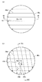
また、本実施形態のIII族窒化物結晶の成長方法において、図1(c)、図3(c)および図4を参照して、下地基板10の主面10mの傾き方向10hと第1のIII族窒化物結晶20の主面20mの傾き方向20hとのなす角度χが、80°以上100°以下であることが好ましい。なお、図4(a)のIC方向の概略断面図が図1(c)に相当し、図4(b)のIIIC方向の概略断面図が図3(c)に相当する。
In the group III nitride crystal growth method of the present embodiment, referring to FIG. 1C, FIG. 3C, and FIG. 4, the
ここで、図4(a)を参照して、第1のIII族窒化物結晶20の転位伝搬線20dを{1−100}面10cに投影した方向は、下地基板10の主面10mの傾き方向10hと同じである。また、図4(b)を参照して、第2のIII族窒化物結晶30の転位伝搬線30dを{1−100}面10cに投影した方向は、第1のIII族窒化物結晶20の主面の傾き方向20hと同じである。
Here, referring to FIG. 4A, the direction in which the
したがって、下地基板10の主面10mの傾き方向10hと第1のIII族窒化物結晶20の主面20mの傾き方向20hを異ならせることにより、第1のIII族窒化物結晶における転位伝搬方向と第2のIII族窒化物結晶における転位伝搬方向を異ならせることができ、第1のIII族窒化物結晶の成長の際に結晶の外周部に排出できなかった転位を第2のIII族窒化物結晶の成長の際に結晶の外周部に排出することができ、III族窒化物結晶の転位密度をより低減することができる。
Therefore, by making the
ここで、図4(b)を参照して、下地基板10の主面10mの傾き方向10hと第1のIII族窒化物結晶20の主面20mの傾き方向20hとのなす角度χ、すなわち第1のIII族窒化物結晶における転位伝搬線を{1−100}面に投影した方向と第2のIII族窒化物結晶における{1−100}面に投影した方向とのなす角度χを80°以上100°以下としたが、この角度範囲であれば実質的に<0001>方向と<11−20>方向(順不問)へ転位を伝播させることができるためである。なお、より効率よく転位を結晶側面より外部に吐き出させるためには、<0001>方向と<11−20>方向の方位差90度に対して、85°以上95°以下であることが望ましい。
Here, referring to FIG. 4B, an angle χ formed by the
また、エピタキシャル成長させる第2のIII族窒化物結晶30は、特に制限はないが、第1のIII族窒化物結晶20との間の格子整合性を高めるため、第1のIII族窒化物結晶20と同じ化学組成を有することが好ましい。
The second group
(実施形態3)
本発明にかかるIII族窒化物結晶の成長方法のさらに他の実施形態は、図5を参照して、実施形態1の成長方法により得られた第1のIII族窒化物結晶20に主面20mを形成する工程(図5(a))と、第1のIII族窒化物結晶20の主面20m上に第3のIII族窒化物結晶40をエピタキシャル成長させる工程(図5(b)とを含む。転位密度が低減した第1のIII族窒化物結晶20の主面20m上に、第3のIII族窒化物結晶40を成長させることにより、成長後の結晶成長面40sの転位密度が低減した第3のIII族窒化物結晶40が得られる。
(Embodiment 3)
Still another embodiment of the III-nitride crystal growth method according to the present invention is described with reference to FIG. 5 in which the first III-
ここで、第1のIII族窒化物結晶20に主面20mを形成する方法には、特に制限はなく、切断、切削、研磨など各種の方法が可能である。また、主面20mの面方位は、特に制限はないが、{1−100}面または{1−100}面との傾き角が小さな面とすることにより、エピタキシャル成長させる第3のIII族窒化物結晶40の結晶成長面40sを{1−100}面とすることができる。こうして、{1−100}面という非極性面である結晶成長面40sにおける転位密度が低減した第3のIII族窒化物結晶40が得られる。
Here, the method for forming the
また、第3のIII族窒化物結晶40の結晶成長方法は、特に制限はなく、本発明の液相法の他、HVPE(ハイドライド気相成長)法、MOCVD(有機金属化学気相堆積)法などの気相法を用いることができる。結晶成長速度が高い観点から、HVPE法が好ましい。
The crystal growth method of the third group
また、エピタキシャル成長させる第3のIII族窒化物結晶40は、特に制限はないが、第1のIII族窒化物結晶20との間の格子整合性を高めるため、第1のIII族窒化物結晶20と同じ化学組成を有することが好ましい。
Further, the third group
(実施形態4)
本発明にかかるIII族窒化物結晶の成長方法のさらに他の実施形態は、図6を参照して、実施形態2の成長方法により得られた第2のIII族窒化物結晶30に主面30mを形成する工程(図6(a))と、第2のIII族窒化物結晶30の主面30m上に第4のIII族窒化物結晶50をエピタキシャル成長させる工程(図6(b))とを含む。転位密度が低減した第2のIII族窒化物結晶30の主面30m上に、第4のIII族窒化物結晶50を成長させることにより、結晶成長後の成長面50sの転位密度が低減した第4のIII族窒化物結晶50が得られる。
(Embodiment 4)
Still another embodiment of the group III nitride crystal growth method according to the present invention is described with reference to FIG. 6 in which the
ここで、第2のIII族窒化物結晶30に主面30mを形成する方法には、特に制限はなく、切断、切削、研磨など各種の方法が可能である。また、主面30mの面方位は、特に制限はないが、{1−100}面または{1−100}面との傾き角が小さな面とすることにより、エピタキシャル成長させる第4のIII族窒化物結晶50の結晶成長面50sを{1−100}面とすることができる。こうして、{1−100}面という非極性面である結晶成長面50sにおける転位密度が低減した第4のIII族窒化物結晶50が得られる。
Here, the method for forming the
また、第4のIII族窒化物結晶50の結晶成長方法は、特に制限はなく、本発明の液相法の他、HVPE(ハイドライド気相成長)法、MOCVD(有機金属化学気相堆積)法などの気相法を用いることができる。結晶成長速度が高い観点から、HVPE法が好ましい。
The crystal growth method of the fourth group
また、エピタキシャル成長させる第4のIII族窒化物結晶50は、特に制限はないが、第2のIII族窒化物結晶30との間の格子整合性を高めるため、第2のIII族窒化物結晶30と同じ化学組成を有することが好ましい。
Further, the fourth group
(実施例1)
図1(a)を参照して、まず、下地基板10として5mm×10mm×厚さ350μmのウルツ鉱型GaN結晶基板を準備した。このGaN基板(下地基板10)は、主面10mが(1−100)面({1−100}面10c)に対して[0001]方向(傾き方向10h)に0.1°の傾き角θ1を有しており、その主面10mが研磨加工により鏡面にされている。このGaN基板(下地基板10)の主面10mにおける面内転位密度をカソードルミネセンス法により暗点として検出し測定したところ、面内平均転位密度は9.0×106cm-2であった。
Example 1
Referring to FIG. 1A, first, a wurtzite GaN crystal substrate having a size of 5 mm × 10 mm × thickness 350 μm was prepared as a
ここで、GaN基板(下地基板10)は、従来の通常の気相法または液相法で厚く成長させた主面を(0001)面とするGaNバルク結晶を、(1−100)面に平行な面でワイヤーソーによりスライスし、スライス面を研磨することよって得られたものである。 Here, the GaN substrate (underlying substrate 10) is a GaN bulk crystal having a (0001) plane as the main surface grown thick by a conventional normal vapor phase method or liquid phase method, and is parallel to the (1-100) plane. It was obtained by slicing with a wire saw on a flat surface and polishing the slice surface.
図1(b)および(c)を参照して、次に、液相法としてNaフラックス法によりGaN基板(下地基板10)の主面10m上に第1のGaN結晶(第1のIII族窒化物結晶20)を厚さ3000μmに成長させた。具体的には、アルミナ製の坩堝(結晶成長容器1)中にGaN基板をその主面10mを上に向けて坩堝底面に置き、20gの金属Ga(純度が99.9モル%)と15gの金属Na(純度が99.9モル%)を入れて、800℃まで加熱し、GaN基板(下地基板10)に接触するGa−Na融液(溶媒3)を形成した。このGa−Na融液(溶媒3)に、純度が99.9モル%で圧力が5MPaの窒素ガス(窒素含有ガス5)を300時間供給し、第1のGaN結晶を平均成長厚さ3000μmに成長させた。平均結晶成長速度は10μmで、第1のGaN結晶の成長後の結晶成長面の面方位は(1−100)であった。
Referring to FIGS. 1B and 1C, next, a first GaN crystal (first group III nitride) is formed on the
次に、成長させた第1のGaN結晶を坩堝から取り出し、その表面を研磨加工し鏡面化した。この鏡面化された第1のGaN結晶の表面について、GaN基板と同様にカソードルミネセンス法により面内平均転位密度を調べたところ、面内平均転位密度は4.0×106cm-2であった。この第1のGaN結晶の転位伝搬の様子を光散乱トモグラフ法により観察したところ、GaN基板に近い成長初期において、転位は(1−100)面に対して実質的に平行な方向に伝搬し、結晶外周側面に到達していることが確認された。また、蛍光顕微鏡により結晶内部を観察したところ、液胞は認められなかった。 Next, the grown first GaN crystal was taken out of the crucible, and its surface was polished to make a mirror surface. When the in-plane average dislocation density of the surface of the mirror-finished first GaN crystal was examined by the cathodoluminescence method in the same manner as the GaN substrate, the in-plane average dislocation density was 4.0 × 10 6 cm −2 . there were. When the dislocation propagation of the first GaN crystal was observed by a light scattering tomography method, the dislocation propagated in a direction substantially parallel to the (1-100) plane in the early growth stage near the GaN substrate. It was confirmed that it reached the outer peripheral side surface of the crystal. Further, when the inside of the crystal was observed with a fluorescence microscope, no vacuole was observed.
(実施例2)
GaN基板(下地基板10)の主面10mが(1−100)面に対して[0001]方向に0.5°の傾き角θ1を有していること以外は、実施例1と同様にして第1のGaN結晶(第1のIII族窒化物結晶20)を成長させ、その表面を鏡面化した。この第1のGaN結晶について、表面における平均転位密度は、3.0×105cm-2であり、GaN基板に近い成長初期において転位は(1−100)面に対して実質的に平行な方向に伝搬し結晶外周側面に到達していることが確認され、結晶内部に液胞は認めらなかった。
(Example 2)
Except that the
(実施例3)
GaN基板(下地基板10)の主面10mが(1−100)面に対して[0001]方向に5°の傾き角θ1を有していること以外は、実施例1と同様にして第1のGaN結晶(第1のIII族窒化物結晶20)を成長させ、その表面を鏡面化した。この第1のGaN結晶について、表面における平均転位密度は、8.0×104cm-2であり、GaN基板に近い成長初期において転位は(1−100)面に対して実質的に平行な方向に伝搬し結晶外周側面に到達していることが確認され、結晶内部に液胞は認めらなかった。
(Example 3)
The first surface is the same as in Example 1 except that the
(実施例4)
GaN基板(下地基板10)の主面10mが(1−100)面に対して[0001]方向に10°の傾き角θ1を有していること以外は、実施例1と同様にして第1のGaN結晶(第1のIII族窒化物結晶20)を成長させ、その表面を鏡面化した。この第1のGaN結晶について、表面における平均転位密度は、6.0×104cm-2であり、GaN基板に近い成長初期において転位は(0001)面に対して実質的に平行な方向に伝搬し結晶外周側面に到達していることが確認され、実用上は問題とならない範囲であるが、結晶内部に極めて少量の液胞が認められた。
Example 4
The first surface is the same as in Example 1 except that the
(比較例1)
GaN基板(下地基板10)の主面10mが(1−100)面(傾き角θ1が0°)であること以外は、実施例1と同様にして第1のGaN結晶(第1のIII族窒化物結晶20)を成長させ、その表面を鏡面化した。この第1のGaN結晶について、表面における平均転位密度は、1.0×107cm-2であり、転位は(1−100)面に対してほぼ垂直な方向に伝搬していることを確認され、結晶内部に液胞は認められなかった。
(Comparative Example 1)
The first GaN crystal (first group III) is the same as in Example 1 except that the
(比較例2)
GaN基板(下地基板10)の主面10mが(1−100)面に対して[0001]方向に11°の傾き角θ1を有していること以外は、実施例1と同様にして第1のGaN結晶(第1のIII族窒化物結晶20)を成長させ、その表面を鏡面化した。この第1のGaN結晶について、表面における平均転位密度は、5.1×104cm-2であり、GaN基板に近い成長初期において転位は(1−100)面に対して実質的に平行な方向に伝搬し結晶外周側面に到達していることが確認されたが、結晶内部に液胞が認められた。
(Comparative Example 2)
The first surface is the same as in Example 1 except that the
(実施例5)
図3(a)を参照して、実施例3で得られた第1のGaN結晶(第1のIII族窒化物結晶20)の表面を研削および研磨することにより、(1−100)面に対して[0001]方向(傾き方向20h)に5°の傾き角θ2を有する主面20mを形成した。本実施例においては、図4を参照して、GaN基板(下地基板10)の主面10mの傾き方向10hと第1のGaN結晶の主面20mの傾き方向20hとのなす角度χは0°であった。
(Example 5)
Referring to FIG. 3A, by grinding and polishing the surface of the first GaN crystal (first group III nitride crystal 20) obtained in Example 3, the (1-100) plane is obtained. On the other hand, a
次に、図3(b)および(c)を参照して、第1のGaN結晶の主面20m上に、実施例1と同様のNaフラックス法により、第2のGaN結晶(第2のIII族窒化物結晶30)を厚さ3000μmに成長させ、その表面を鏡面化した。この第2のGaN結晶について、表面における平均転位密度は5.0×104cm-2と実施例3の第1のGaN結晶の平均転位密度(8.0×104cm-2)に比べてわずかに減少し、第1のGaN結晶に近い成長初期において転位は(1−100)面に対して実質的に平行な方向に伝搬し結晶外周側面に到達していることが確認され、結晶内部に液胞は認めらなかった。
Next, with reference to FIGS. 3B and 3C, the second GaN crystal (second III) is formed on the
(実施例6)
図3(a)を参照して、実施例3で得られた第1のGaN結晶(第1のIII族窒化物結晶20)の表面を研削および研磨することにより、(1−100)面に対して[11−20]方向(傾き方向20h)に5°の傾き角θ2を有する主面20mを形成した。本実施例においては、図4を参照して、GaN基板(下地基板10)の主面10mの傾き方向10hと第1のGaN結晶の主面20mの傾き方向20hとのなす角度χは90°であった。
(Example 6)
Referring to FIG. 3A, by grinding and polishing the surface of the first GaN crystal (first group III nitride crystal 20) obtained in Example 3, the (1-100) plane is obtained. On the other hand, a
次に、図3(b)および(c)を参照して、第1のGaN結晶の主面20m上に、実施例1と同様のNaフラックス法により、第2のGaN結晶(第2のIII族窒化物結晶30)を厚さ3000μmに成長させ、その表面を鏡面化した。この第2のGaN結晶について、表面における平均転位密度は6.0×103cm-2と実施例3の第1のGaN結晶の平均転位密度(8.0×104cm-2)に比べて著しく減少し、第1のGaN結晶に近い成長初期において転位は(1−100)面に対して実質的に平行な方向に伝搬し結晶外周側面に到達していることが確認され、結晶内部に液胞は認めらなかった。
Next, with reference to FIGS. 3B and 3C, the second GaN crystal (second III) is formed on the
実施例1〜4および比較例1,2から、主面が{1−100}面に対して0.1°以上10°以下の傾き角をする下地基板のその主面上に、第1のIII族窒化物結晶をエピタキシャル成長させることにより、第1のIII族窒化物結晶に存在する転位の少なくとも一部が{1−100}面に対して実質的に平行な方向に伝搬して第1のIII族窒化物結晶の外周部に排出され、結晶成長後の結晶成長面における転位密度が低減した第1のIII族窒化物結晶が得られることがわかった。 From Examples 1 to 4 and Comparative Examples 1 and 2, on the main surface of the base substrate in which the main surface has an inclination angle of 0.1 ° to 10 ° with respect to the {1-100} plane, By epitaxially growing the group III nitride crystal, at least some of the dislocations present in the first group III nitride crystal propagate in a direction substantially parallel to the {1-100} plane, It was found that a first group III nitride crystal having a reduced dislocation density on the crystal growth surface after crystal growth was discharged to the outer periphery of the group III nitride crystal.
また、実施例3、5および6から、上記第1のIII族窒化物結晶に{1−100}に対して0.1°以上10°以下の傾き角を有する主面を形成し、この第1のIII族窒化物結晶の主面上に第2のIII族窒化物結晶をエピタキシャル成長させることにより、第2のIII族窒化物結晶に存在する転位の少なくとも一部が{1−100}面に対して実質的に平行な方向に伝搬して第2のIII族窒化物結晶の外周部に排出され、結晶成長後の結晶成長面における転位密度が低減した第2のIII族窒化物結晶が得られることがわかった。ここで、下地基板の主面の傾き方向と第1のIII族窒化物結晶の主面の傾き方向とのなす角が80°以上100°以下であると、第2のIII族窒化物結晶の転位密度は、下地基板および第1のIII族窒化物結晶の転位密度に比べて、著しく低減することがわかった。 Further, from Examples 3, 5 and 6, a main surface having an inclination angle of 0.1 ° to 10 ° with respect to {1-100} is formed in the first group III nitride crystal. By epitaxially growing the second group III nitride crystal on the main surface of the first group III nitride crystal, at least some of the dislocations present in the second group III nitride crystal are converted to the {1-100} plane. The second group III nitride crystal having a reduced dislocation density on the crystal growth surface after the crystal growth is obtained by propagating in a substantially parallel direction to the outer periphery of the second group III nitride crystal. I found out that Here, when the angle between the tilt direction of the main surface of the base substrate and the tilt direction of the main surface of the first group III nitride crystal is 80 ° or more and 100 ° or less, the second group III nitride crystal of It has been found that the dislocation density is significantly reduced compared to the dislocation density of the base substrate and the first group III nitride crystal.
今回開示された実施の形態および実施例はすべての点で例示であって制限的なものではないと考えられるべきである。本発明の範囲は、上記した説明でなくて特許請求の範囲によって示され、特許請求の範囲と均等の意味および範囲内のすべての変更が含まれることが意図される。 It should be understood that the embodiments and examples disclosed herein are illustrative and non-restrictive in every respect. The scope of the present invention is defined by the terms of the claims, rather than the description above, and is intended to include any modifications within the scope and meaning equivalent to the terms of the claims.
1 結晶成長容器、3 溶媒、5 窒素含有ガス、10 下地基板、10a III族窒化物結晶層、10c,20c,30c {1−100}面、10h,20h 傾き方向、10m,20m,30m 主面、10mc,20ac,20bc テラス面、10s,20as,20bs ステップ、10t,20at,20bt ステップ面、20,30,40,50 III族窒化物結晶、20a,20b,20e,20s,30s,40s,50s 結晶成長面、20d,30d 転位伝搬線。 1 crystal growth vessel, 3 solvent, 5 nitrogen-containing gas, 10 base substrate, 10a group III nitride crystal layer, 10c, 20c, 30c {1-100} plane, 10h, 20h tilt direction, 10m, 20m, 30m main surface 10mc, 20ac, 20bc Terrace surface, 10s, 20as, 20bs step, 10t, 20at, 20bt step surface, 20, 30, 40, 50 Group III nitride crystal, 20a, 20b, 20e, 20s, 30s, 40s, 50s Crystal growth surface, 20d, 30d dislocation propagation lines.
Claims (9)
前記下地基板の前記主面にIII族金属とアルカリ金属を含む溶媒に窒素含有ガスを溶解させた溶液を接触させて、前記下地基板の前記主面上に第1のIII族窒化物結晶をエピタキシャル成長させる工程をさらに備え、
前記第1のIII族窒化物結晶の成長後の結晶成長面における転位密度が前記下地基板の前記主面における転位密度の1/10以下であるIII族窒化物結晶の成長方法。 Comprising the step of providing a base substrate, said base substrate comprises a III nitride seed crystal having a first principal surface, before Symbol principal surface with respect to {1-100} plane of the Group III nitride crystal 0.1 Having a tilt angle of not less than 10 ° and not more than 10 °, and the dislocation density in the main surface is less than 1 × 10 7 cm −2 ,
A first group III nitride crystal is epitaxially grown on the main surface of the base substrate by contacting the main surface of the base substrate with a solution in which a nitrogen-containing gas is dissolved in a solvent containing a group III metal and an alkali metal. further comprising the step of,
It said first group III nitride 1/10 der Ru III-growth method of the nitride crystal following the dislocation density dislocation density in the crystal growth surface after growth in the primary surface of the underlying substrate crystals.
前記第1のIII族窒化物結晶の主面にIII族金属とアルカリ金属を含む溶媒に窒素含有ガスを溶解させた溶液を接触させて、前記第1のIII族窒化物結晶の前記主面上に第2のIII族窒化物結晶をエピタキシャル成長させる工程をさらに備えるIII族窒化物結晶の成長方法。 The method further comprises a step of forming a main surface on the first group III nitride crystal obtained by the growth method according to claim 1, wherein the main surface of the first group III nitride crystal is the {1-100} An inclination angle of 0.1 ° to 10 ° with respect to the surface;
The main surface of the first group III nitride crystal is brought into contact with the main surface of the first group III nitride crystal by contacting a solution containing a nitrogen-containing gas in a solvent containing a group III metal and an alkali metal. A method for growing a group III nitride crystal, further comprising the step of epitaxially growing a second group III nitride crystal.
前記第2のIII族窒化物結晶の成長後の結晶成長面における転位密度が前記下地基板の前記主面における転位密度の1/100以下である請求項3に記載のIII族窒化物結晶の成長方法。 A dislocation density in the main surface of the base substrate is less than 1 × 10 7 cm −2 ;
4. The growth of a group III nitride crystal according to claim 3 , wherein a dislocation density on a crystal growth surface after the growth of the second group III nitride crystal is 1/100 or less of a dislocation density on the main surface of the base substrate. Method.
Priority Applications (1)
| Application Number | Priority Date | Filing Date | Title |
|---|---|---|---|
| JP2007245838A JP5144192B2 (en) | 2007-09-21 | 2007-09-21 | Group III nitride crystal growth method |
Applications Claiming Priority (1)
| Application Number | Priority Date | Filing Date | Title |
|---|---|---|---|
| JP2007245838A JP5144192B2 (en) | 2007-09-21 | 2007-09-21 | Group III nitride crystal growth method |
Publications (2)
| Publication Number | Publication Date |
|---|---|
| JP2009073704A JP2009073704A (en) | 2009-04-09 |
| JP5144192B2 true JP5144192B2 (en) | 2013-02-13 |
Family
ID=40609070
Family Applications (1)
| Application Number | Title | Priority Date | Filing Date |
|---|---|---|---|
| JP2007245838A Expired - Fee Related JP5144192B2 (en) | 2007-09-21 | 2007-09-21 | Group III nitride crystal growth method |
Country Status (1)
| Country | Link |
|---|---|
| JP (1) | JP5144192B2 (en) |
Families Citing this family (6)
| Publication number | Priority date | Publication date | Assignee | Title |
|---|---|---|---|---|
| JP2011016676A (en) * | 2009-07-07 | 2011-01-27 | Sumitomo Electric Ind Ltd | Method for producing nitride semiconductor substrate |
| JP5549158B2 (en) * | 2009-09-04 | 2014-07-16 | 住友電気工業株式会社 | GaN single crystal substrate and manufacturing method thereof, and GaN-based semiconductor device and manufacturing method thereof |
| US8598685B2 (en) | 2009-09-04 | 2013-12-03 | Sumitomo Electric Industries, Ltd. | GaN single crystal substrate and method of manufacturing thereof and GaN-based semiconductor device and method of manufacturing thereof |
| JP6137197B2 (en) | 2012-12-17 | 2017-05-31 | 三菱化学株式会社 | Gallium nitride substrate and method of manufacturing nitride semiconductor crystal |
| JP2014001138A (en) * | 2013-09-25 | 2014-01-09 | Sumitomo Electric Ind Ltd | GaN SINGLE CRYSTAL SUBSTRATE AND METHOD OF MANUFACTURING THE SAME, AND GaN-BASED SEMICONDUCTOR DEVICE AND METHOD OF MANUFACTURING THE SAME |
| JP2014001137A (en) * | 2013-09-25 | 2014-01-09 | Sumitomo Electric Ind Ltd | GaN SINGLE CRYSTAL SUBSTRATE AND METHOD OF MANUFACTURING THE SAME, AND GaN-BASED SEMICONDUCTOR DEVICE AND METHOD OF MANUFACTURING THE SAME |
Family Cites Families (6)
| Publication number | Priority date | Publication date | Assignee | Title |
|---|---|---|---|---|
| JP2002145700A (en) * | 2000-08-14 | 2002-05-22 | Nippon Telegr & Teleph Corp <Ntt> | Sapphire substrate, semiconductor device, electronic component and crystal growth method |
| JP4278330B2 (en) * | 2002-01-10 | 2009-06-10 | 株式会社リコー | Group III nitride crystal production method and group III nitride crystal production apparatus |
| JP4397695B2 (en) * | 2003-01-20 | 2010-01-13 | パナソニック株式会社 | Method for manufacturing group III nitride substrate |
| JP2006193348A (en) * | 2005-01-11 | 2006-07-27 | Sumitomo Electric Ind Ltd | Group III nitride semiconductor substrate and manufacturing method thereof |
| JP2007119325A (en) * | 2005-10-31 | 2007-05-17 | Sumitomo Electric Ind Ltd | Group III nitride crystal and growth method thereof |
| JP2007161536A (en) * | 2005-12-14 | 2007-06-28 | Sumitomo Electric Ind Ltd | AlxGayIn1-xyN crystal substrate, semiconductor device and manufacturing method thereof |
-
2007
- 2007-09-21 JP JP2007245838A patent/JP5144192B2/en not_active Expired - Fee Related
Also Published As
| Publication number | Publication date |
|---|---|
| JP2009073704A (en) | 2009-04-09 |
Similar Documents
| Publication | Publication Date | Title |
|---|---|---|
| JP6218788B2 (en) | Process for growth of low dislocation density GaN | |
| JP5656697B2 (en) | Method for producing aluminum nitride crystal | |
| JP4741506B2 (en) | Large area and uniform low dislocation density GaN substrate and its manufacturing process | |
| JP6019542B2 (en) | Group III nitride crystal manufacturing method and group III nitride crystal manufacturing apparatus | |
| JP4397695B2 (en) | Method for manufacturing group III nitride substrate | |
| JP2009167053A (en) | Group III nitride crystal growth method | |
| WO2016140074A1 (en) | Method for manufacturing group-iii nitride semiconductor crystal substrate | |
| JP5015417B2 (en) | GaN crystal manufacturing method | |
| JP5144192B2 (en) | Group III nitride crystal growth method | |
| JP2007197276A (en) | III-V nitride semiconductor substrate, method of manufacturing the same, and III-V nitride light emitting device | |
| JP2015166293A (en) | Group III nitride crystal manufacturing method, group III nitride crystal, semiconductor device, and group III nitride crystal manufacturing apparatus | |
| JP5333374B2 (en) | GaN crystal manufacturing method, GaN crystal substrate, and group III nitride semiconductor device | |
| JP6143148B2 (en) | Group III nitride crystal manufacturing method and semiconductor device manufacturing method | |
| WO2020158571A1 (en) | Nitride semiconductor substrate, laminated structure, and method for manufacturing nitride semiconductor substrate | |
| JP6249250B2 (en) | Group III nitride semiconductor and method of manufacturing the same | |
| US20250129513A1 (en) | Production method for nitride crystal substrate and nitride crystal substrate | |
| JP7457932B2 (en) | Method for manufacturing nitride semiconductor crystal and nitride semiconductor crystal substrate | |
| JP6596692B2 (en) | Group III element nitride crystal manufacturing method, group III element nitride crystal, semiconductor device, semiconductor device manufacturing method, and group III element nitride crystal manufacturing apparatus | |
| JP2008273768A (en) | Group III nitride crystal growth method and group III nitride crystal substrate | |
| US12606934B2 (en) | Group III nitride crystal, group III nitride semiconductor, group III nitride substrate, and method for producing group III nitride crystal | |
| JP2009051686A (en) | Group III nitride crystal growth method | |
| CN103534391A (en) | Process for producing group 13 metal nitride, and seed crystal substrate for use in same | |
| JP5045589B2 (en) | Group III nitride crystal growth method | |
| JP2009057247A (en) | Group III nitride crystal growth method and group III nitride crystal substrate | |
| JP2014028722A (en) | Method for producing group 13 element nitride crystal |
Legal Events
| Date | Code | Title | Description |
|---|---|---|---|
| A621 | Written request for application examination |
Free format text: JAPANESE INTERMEDIATE CODE: A621 Effective date: 20100423 |
|
| A977 | Report on retrieval |
Free format text: JAPANESE INTERMEDIATE CODE: A971007 Effective date: 20110823 |
|
| A131 | Notification of reasons for refusal |
Free format text: JAPANESE INTERMEDIATE CODE: A131 Effective date: 20110913 |
|
| A131 | Notification of reasons for refusal |
Free format text: JAPANESE INTERMEDIATE CODE: A131 Effective date: 20120821 |
|
| A521 | Request for written amendment filed |
Free format text: JAPANESE INTERMEDIATE CODE: A523 Effective date: 20121011 |
|
| TRDD | Decision of grant or rejection written | ||
| A01 | Written decision to grant a patent or to grant a registration (utility model) |
Free format text: JAPANESE INTERMEDIATE CODE: A01 Effective date: 20121106 |
|
| A01 | Written decision to grant a patent or to grant a registration (utility model) |
Free format text: JAPANESE INTERMEDIATE CODE: A01 |
|
| A61 | First payment of annual fees (during grant procedure) |
Free format text: JAPANESE INTERMEDIATE CODE: A61 Effective date: 20121122 |
|
| FPAY | Renewal fee payment (event date is renewal date of database) |
Free format text: PAYMENT UNTIL: 20151130 Year of fee payment: 3 |
|
| R150 | Certificate of patent or registration of utility model |
Ref document number: 5144192 Country of ref document: JP Free format text: JAPANESE INTERMEDIATE CODE: R150 Free format text: JAPANESE INTERMEDIATE CODE: R150 |
|
| R250 | Receipt of annual fees |
Free format text: JAPANESE INTERMEDIATE CODE: R250 |
|
| R250 | Receipt of annual fees |
Free format text: JAPANESE INTERMEDIATE CODE: R250 |
|
| R250 | Receipt of annual fees |
Free format text: JAPANESE INTERMEDIATE CODE: R250 |
|
| R250 | Receipt of annual fees |
Free format text: JAPANESE INTERMEDIATE CODE: R250 |
|
| R250 | Receipt of annual fees |
Free format text: JAPANESE INTERMEDIATE CODE: R250 |
|
| R250 | Receipt of annual fees |
Free format text: JAPANESE INTERMEDIATE CODE: R250 |
|
| R250 | Receipt of annual fees |
Free format text: JAPANESE INTERMEDIATE CODE: R250 |
|
| R250 | Receipt of annual fees |
Free format text: JAPANESE INTERMEDIATE CODE: R250 |
|
| LAPS | Cancellation because of no payment of annual fees |