JP5122817B2 - LED production by ion implant isolation - Google Patents
LED production by ion implant isolation Download PDFInfo
- Publication number
- JP5122817B2 JP5122817B2 JP2006532792A JP2006532792A JP5122817B2 JP 5122817 B2 JP5122817 B2 JP 5122817B2 JP 2006532792 A JP2006532792 A JP 2006532792A JP 2006532792 A JP2006532792 A JP 2006532792A JP 5122817 B2 JP5122817 B2 JP 5122817B2
- Authority
- JP
- Japan
- Prior art keywords
- light emitting
- emitting diode
- substrate
- epitaxial
- type
- Prior art date
- Legal status (The legal status is an assumption and is not a legal conclusion. Google has not performed a legal analysis and makes no representation as to the accuracy of the status listed.)
- Active
Links
- 238000002955 isolation Methods 0.000 title claims description 12
- 239000007943 implant Substances 0.000 title description 24
- 238000004519 manufacturing process Methods 0.000 title description 11
- 229910052751 metal Inorganic materials 0.000 claims description 65
- 239000002184 metal Substances 0.000 claims description 65
- 239000000758 substrate Substances 0.000 claims description 60
- 229910002601 GaN Inorganic materials 0.000 claims description 41
- JMASRVWKEDWRBT-UHFFFAOYSA-N Gallium nitride Chemical compound [Ga]#N JMASRVWKEDWRBT-UHFFFAOYSA-N 0.000 claims description 32
- 239000000463 material Substances 0.000 claims description 26
- HBMJWWWQQXIZIP-UHFFFAOYSA-N silicon carbide Chemical compound [Si+]#[C-] HBMJWWWQQXIZIP-UHFFFAOYSA-N 0.000 claims description 26
- 229910010271 silicon carbide Inorganic materials 0.000 claims description 26
- 239000004065 semiconductor Substances 0.000 claims description 15
- 150000004767 nitrides Chemical class 0.000 claims description 12
- VYPSYNLAJGMNEJ-UHFFFAOYSA-N Silicium dioxide Chemical compound O=[Si]=O VYPSYNLAJGMNEJ-UHFFFAOYSA-N 0.000 claims description 8
- PXHVJJICTQNCMI-UHFFFAOYSA-N Nickel Chemical compound [Ni] PXHVJJICTQNCMI-UHFFFAOYSA-N 0.000 claims description 6
- 238000002161 passivation Methods 0.000 claims description 6
- BASFCYQUMIYNBI-UHFFFAOYSA-N platinum Chemical group [Pt] BASFCYQUMIYNBI-UHFFFAOYSA-N 0.000 claims description 6
- 229910052581 Si3N4 Inorganic materials 0.000 claims description 5
- 229910052782 aluminium Inorganic materials 0.000 claims description 5
- XAGFODPZIPBFFR-UHFFFAOYSA-N aluminium Chemical compound [Al] XAGFODPZIPBFFR-UHFFFAOYSA-N 0.000 claims description 5
- HQVNEWCFYHHQES-UHFFFAOYSA-N silicon nitride Chemical compound N12[Si]34N5[Si]62N3[Si]51N64 HQVNEWCFYHHQES-UHFFFAOYSA-N 0.000 claims description 5
- PCHJSUWPFVWCPO-UHFFFAOYSA-N gold Chemical compound [Au] PCHJSUWPFVWCPO-UHFFFAOYSA-N 0.000 claims description 4
- 229910052737 gold Inorganic materials 0.000 claims description 4
- 239000010931 gold Substances 0.000 claims description 4
- 229910052594 sapphire Inorganic materials 0.000 claims description 4
- 239000010980 sapphire Substances 0.000 claims description 4
- 235000012239 silicon dioxide Nutrition 0.000 claims description 4
- 239000000377 silicon dioxide Substances 0.000 claims description 4
- BQCADISMDOOEFD-UHFFFAOYSA-N Silver Chemical compound [Ag] BQCADISMDOOEFD-UHFFFAOYSA-N 0.000 claims description 3
- RTAQQCXQSZGOHL-UHFFFAOYSA-N Titanium Chemical compound [Ti] RTAQQCXQSZGOHL-UHFFFAOYSA-N 0.000 claims description 3
- CPLXHLVBOLITMK-UHFFFAOYSA-N magnesium oxide Inorganic materials [Mg]=O CPLXHLVBOLITMK-UHFFFAOYSA-N 0.000 claims description 3
- 229910052759 nickel Inorganic materials 0.000 claims description 3
- 229910052697 platinum Inorganic materials 0.000 claims description 3
- 229920000642 polymer Polymers 0.000 claims description 3
- 229910052709 silver Inorganic materials 0.000 claims description 3
- 239000004332 silver Substances 0.000 claims description 3
- 229910052719 titanium Inorganic materials 0.000 claims description 3
- 239000010936 titanium Substances 0.000 claims description 3
- PMHQVHHXPFUNSP-UHFFFAOYSA-M copper(1+);methylsulfanylmethane;bromide Chemical compound Br[Cu].CSC PMHQVHHXPFUNSP-UHFFFAOYSA-M 0.000 claims description 2
- 229910052596 spinel Inorganic materials 0.000 claims description 2
- 239000011029 spinel Substances 0.000 claims description 2
- XUIMIQQOPSSXEZ-UHFFFAOYSA-N Silicon Chemical compound [Si] XUIMIQQOPSSXEZ-UHFFFAOYSA-N 0.000 claims 1
- 239000000395 magnesium oxide Substances 0.000 claims 1
- 229910052710 silicon Inorganic materials 0.000 claims 1
- 239000010703 silicon Substances 0.000 claims 1
- XLOMVQKBTHCTTD-UHFFFAOYSA-N zinc oxide Inorganic materials [Zn]=O XLOMVQKBTHCTTD-UHFFFAOYSA-N 0.000 claims 1
- 239000011787 zinc oxide Substances 0.000 claims 1
- 239000010410 layer Substances 0.000 description 111
- 238000000034 method Methods 0.000 description 31
- IJGRMHOSHXDMSA-UHFFFAOYSA-N Atomic nitrogen Chemical compound N#N IJGRMHOSHXDMSA-UHFFFAOYSA-N 0.000 description 18
- 150000002500 ions Chemical class 0.000 description 15
- 229920002120 photoresistant polymer Polymers 0.000 description 15
- 238000005530 etching Methods 0.000 description 14
- 229910052757 nitrogen Inorganic materials 0.000 description 9
- 230000008569 process Effects 0.000 description 9
- 238000002513 implantation Methods 0.000 description 8
- 239000002243 precursor Substances 0.000 description 8
- 235000012431 wafers Nutrition 0.000 description 8
- 238000000926 separation method Methods 0.000 description 6
- 238000011156 evaluation Methods 0.000 description 5
- 230000000873 masking effect Effects 0.000 description 5
- 238000013461 design Methods 0.000 description 4
- 238000004806 packaging method and process Methods 0.000 description 4
- 238000000206 photolithography Methods 0.000 description 4
- 230000004888 barrier function Effects 0.000 description 3
- 238000010586 diagram Methods 0.000 description 3
- 230000003071 parasitic effect Effects 0.000 description 3
- 230000002093 peripheral effect Effects 0.000 description 3
- 239000000126 substance Substances 0.000 description 3
- -1 thicknesses Substances 0.000 description 3
- KDLHZDBZIXYQEI-UHFFFAOYSA-N Palladium Chemical compound [Pd] KDLHZDBZIXYQEI-UHFFFAOYSA-N 0.000 description 2
- ATJFFYVFTNAWJD-UHFFFAOYSA-N Tin Chemical compound [Sn] ATJFFYVFTNAWJD-UHFFFAOYSA-N 0.000 description 2
- 239000000969 carrier Substances 0.000 description 2
- 230000008859 change Effects 0.000 description 2
- 238000007796 conventional method Methods 0.000 description 2
- 230000000694 effects Effects 0.000 description 2
- 230000005611 electricity Effects 0.000 description 2
- 239000001307 helium Substances 0.000 description 2
- 229910052734 helium Inorganic materials 0.000 description 2
- SWQJXJOGLNCZEY-UHFFFAOYSA-N helium atom Chemical compound [He] SWQJXJOGLNCZEY-UHFFFAOYSA-N 0.000 description 2
- 239000011810 insulating material Substances 0.000 description 2
- 238000000059 patterning Methods 0.000 description 2
- 238000001020 plasma etching Methods 0.000 description 2
- 238000012545 processing Methods 0.000 description 2
- 239000003566 sealing material Substances 0.000 description 2
- ZAMOUSCENKQFHK-UHFFFAOYSA-N Chlorine atom Chemical compound [Cl] ZAMOUSCENKQFHK-UHFFFAOYSA-N 0.000 description 1
- 239000004593 Epoxy Substances 0.000 description 1
- OAICVXFJPJFONN-UHFFFAOYSA-N Phosphorus Chemical compound [P] OAICVXFJPJFONN-UHFFFAOYSA-N 0.000 description 1
- 239000004952 Polyamide Substances 0.000 description 1
- 230000002159 abnormal effect Effects 0.000 description 1
- 239000012790 adhesive layer Substances 0.000 description 1
- 239000000956 alloy Substances 0.000 description 1
- 229910045601 alloy Inorganic materials 0.000 description 1
- RNQKDQAVIXDKAG-UHFFFAOYSA-N aluminum gallium Chemical compound [Al].[Ga] RNQKDQAVIXDKAG-UHFFFAOYSA-N 0.000 description 1
- 125000004429 atom Chemical group 0.000 description 1
- 230000015556 catabolic process Effects 0.000 description 1
- 239000000460 chlorine Substances 0.000 description 1
- 229910052801 chlorine Inorganic materials 0.000 description 1
- 150000001875 compounds Chemical class 0.000 description 1
- 239000004020 conductor Substances 0.000 description 1
- 239000000356 contaminant Substances 0.000 description 1
- 238000011109 contamination Methods 0.000 description 1
- 239000013078 crystal Substances 0.000 description 1
- 238000000151 deposition Methods 0.000 description 1
- 230000001627 detrimental effect Effects 0.000 description 1
- 238000011161 development Methods 0.000 description 1
- 230000018109 developmental process Effects 0.000 description 1
- 239000003989 dielectric material Substances 0.000 description 1
- 238000009792 diffusion process Methods 0.000 description 1
- 239000002019 doping agent Substances 0.000 description 1
- 239000008393 encapsulating agent Substances 0.000 description 1
- 230000007613 environmental effect Effects 0.000 description 1
- 239000002360 explosive Substances 0.000 description 1
- 239000007789 gas Substances 0.000 description 1
- 239000011521 glass Substances 0.000 description 1
- 239000001257 hydrogen Substances 0.000 description 1
- 229910052739 hydrogen Inorganic materials 0.000 description 1
- 125000004435 hydrogen atom Chemical class [H]* 0.000 description 1
- 239000012212 insulator Substances 0.000 description 1
- 230000003993 interaction Effects 0.000 description 1
- 239000007788 liquid Substances 0.000 description 1
- 238000012423 maintenance Methods 0.000 description 1
- 239000000155 melt Substances 0.000 description 1
- 239000000203 mixture Substances 0.000 description 1
- 230000003287 optical effect Effects 0.000 description 1
- 239000005022 packaging material Substances 0.000 description 1
- 229910052763 palladium Inorganic materials 0.000 description 1
- 229910052698 phosphorus Inorganic materials 0.000 description 1
- 239000011574 phosphorus Substances 0.000 description 1
- 230000000704 physical effect Effects 0.000 description 1
- 238000000623 plasma-assisted chemical vapour deposition Methods 0.000 description 1
- 229920002647 polyamide Polymers 0.000 description 1
- 239000002952 polymeric resin Substances 0.000 description 1
- 238000011084 recovery Methods 0.000 description 1
- 239000000523 sample Substances 0.000 description 1
- SBIBMFFZSBJNJF-UHFFFAOYSA-N selenium;zinc Chemical compound [Se]=[Zn] SBIBMFFZSBJNJF-UHFFFAOYSA-N 0.000 description 1
- 230000009919 sequestration Effects 0.000 description 1
- 238000004088 simulation Methods 0.000 description 1
- 239000002356 single layer Substances 0.000 description 1
- 229910000679 solder Inorganic materials 0.000 description 1
- 238000005476 soldering Methods 0.000 description 1
- 239000007787 solid Substances 0.000 description 1
- 239000002904 solvent Substances 0.000 description 1
- 238000001228 spectrum Methods 0.000 description 1
- 230000007480 spreading Effects 0.000 description 1
- 238000003892 spreading Methods 0.000 description 1
- 238000004544 sputter deposition Methods 0.000 description 1
- 229920003002 synthetic resin Polymers 0.000 description 1
- 230000007704 transition Effects 0.000 description 1
- 238000001429 visible spectrum Methods 0.000 description 1
Images


Classifications
-
- H—ELECTRICITY
- H01—ELECTRIC ELEMENTS
- H01L—SEMICONDUCTOR DEVICES NOT COVERED BY CLASS H10
- H01L33/00—Semiconductor devices with at least one potential-jump barrier or surface barrier specially adapted for light emission; Processes or apparatus specially adapted for the manufacture or treatment thereof or of parts thereof; Details thereof
- H01L33/02—Semiconductor devices with at least one potential-jump barrier or surface barrier specially adapted for light emission; Processes or apparatus specially adapted for the manufacture or treatment thereof or of parts thereof; Details thereof characterised by the semiconductor bodies
- H01L33/14—Semiconductor devices with at least one potential-jump barrier or surface barrier specially adapted for light emission; Processes or apparatus specially adapted for the manufacture or treatment thereof or of parts thereof; Details thereof characterised by the semiconductor bodies with a carrier transport control structure, e.g. highly-doped semiconductor layer or current-blocking structure
- H01L33/145—Semiconductor devices with at least one potential-jump barrier or surface barrier specially adapted for light emission; Processes or apparatus specially adapted for the manufacture or treatment thereof or of parts thereof; Details thereof characterised by the semiconductor bodies with a carrier transport control structure, e.g. highly-doped semiconductor layer or current-blocking structure with a current-blocking structure
-
- H—ELECTRICITY
- H01—ELECTRIC ELEMENTS
- H01L—SEMICONDUCTOR DEVICES NOT COVERED BY CLASS H10
- H01L33/00—Semiconductor devices with at least one potential-jump barrier or surface barrier specially adapted for light emission; Processes or apparatus specially adapted for the manufacture or treatment thereof or of parts thereof; Details thereof
- H01L33/005—Processes
- H01L33/0095—Post-treatment of devices, e.g. annealing, recrystallisation or short-circuit elimination
-
- H—ELECTRICITY
- H01—ELECTRIC ELEMENTS
- H01L—SEMICONDUCTOR DEVICES NOT COVERED BY CLASS H10
- H01L33/00—Semiconductor devices with at least one potential-jump barrier or surface barrier specially adapted for light emission; Processes or apparatus specially adapted for the manufacture or treatment thereof or of parts thereof; Details thereof
- H01L33/02—Semiconductor devices with at least one potential-jump barrier or surface barrier specially adapted for light emission; Processes or apparatus specially adapted for the manufacture or treatment thereof or of parts thereof; Details thereof characterised by the semiconductor bodies
- H01L33/025—Physical imperfections, e.g. particular concentration or distribution of impurities
-
- H—ELECTRICITY
- H01—ELECTRIC ELEMENTS
- H01L—SEMICONDUCTOR DEVICES NOT COVERED BY CLASS H10
- H01L33/00—Semiconductor devices with at least one potential-jump barrier or surface barrier specially adapted for light emission; Processes or apparatus specially adapted for the manufacture or treatment thereof or of parts thereof; Details thereof
- H01L33/02—Semiconductor devices with at least one potential-jump barrier or surface barrier specially adapted for light emission; Processes or apparatus specially adapted for the manufacture or treatment thereof or of parts thereof; Details thereof characterised by the semiconductor bodies
- H01L33/26—Materials of the light emitting region
- H01L33/30—Materials of the light emitting region containing only elements of group III and group V of the periodic system
- H01L33/32—Materials of the light emitting region containing only elements of group III and group V of the periodic system containing nitrogen
-
- H—ELECTRICITY
- H01—ELECTRIC ELEMENTS
- H01L—SEMICONDUCTOR DEVICES NOT COVERED BY CLASS H10
- H01L2224/00—Indexing scheme for arrangements for connecting or disconnecting semiconductor or solid-state bodies and methods related thereto as covered by H01L24/00
- H01L2224/01—Means for bonding being attached to, or being formed on, the surface to be connected, e.g. chip-to-package, die-attach, "first-level" interconnects; Manufacturing methods related thereto
- H01L2224/26—Layer connectors, e.g. plate connectors, solder or adhesive layers; Manufacturing methods related thereto
- H01L2224/31—Structure, shape, material or disposition of the layer connectors after the connecting process
- H01L2224/32—Structure, shape, material or disposition of the layer connectors after the connecting process of an individual layer connector
- H01L2224/321—Disposition
- H01L2224/32151—Disposition the layer connector connecting between a semiconductor or solid-state body and an item not being a semiconductor or solid-state body, e.g. chip-to-substrate, chip-to-passive
- H01L2224/32221—Disposition the layer connector connecting between a semiconductor or solid-state body and an item not being a semiconductor or solid-state body, e.g. chip-to-substrate, chip-to-passive the body and the item being stacked
- H01L2224/32245—Disposition the layer connector connecting between a semiconductor or solid-state body and an item not being a semiconductor or solid-state body, e.g. chip-to-substrate, chip-to-passive the body and the item being stacked the item being metallic
-
- H—ELECTRICITY
- H01—ELECTRIC ELEMENTS
- H01L—SEMICONDUCTOR DEVICES NOT COVERED BY CLASS H10
- H01L2224/00—Indexing scheme for arrangements for connecting or disconnecting semiconductor or solid-state bodies and methods related thereto as covered by H01L24/00
- H01L2224/01—Means for bonding being attached to, or being formed on, the surface to be connected, e.g. chip-to-package, die-attach, "first-level" interconnects; Manufacturing methods related thereto
- H01L2224/42—Wire connectors; Manufacturing methods related thereto
- H01L2224/47—Structure, shape, material or disposition of the wire connectors after the connecting process
- H01L2224/48—Structure, shape, material or disposition of the wire connectors after the connecting process of an individual wire connector
- H01L2224/4805—Shape
- H01L2224/4809—Loop shape
- H01L2224/48091—Arched
-
- H—ELECTRICITY
- H01—ELECTRIC ELEMENTS
- H01L—SEMICONDUCTOR DEVICES NOT COVERED BY CLASS H10
- H01L2224/00—Indexing scheme for arrangements for connecting or disconnecting semiconductor or solid-state bodies and methods related thereto as covered by H01L24/00
- H01L2224/01—Means for bonding being attached to, or being formed on, the surface to be connected, e.g. chip-to-package, die-attach, "first-level" interconnects; Manufacturing methods related thereto
- H01L2224/42—Wire connectors; Manufacturing methods related thereto
- H01L2224/47—Structure, shape, material or disposition of the wire connectors after the connecting process
- H01L2224/48—Structure, shape, material or disposition of the wire connectors after the connecting process of an individual wire connector
- H01L2224/481—Disposition
- H01L2224/48151—Connecting between a semiconductor or solid-state body and an item not being a semiconductor or solid-state body, e.g. chip-to-substrate, chip-to-passive
- H01L2224/48221—Connecting between a semiconductor or solid-state body and an item not being a semiconductor or solid-state body, e.g. chip-to-substrate, chip-to-passive the body and the item being stacked
- H01L2224/48245—Connecting between a semiconductor or solid-state body and an item not being a semiconductor or solid-state body, e.g. chip-to-substrate, chip-to-passive the body and the item being stacked the item being metallic
- H01L2224/48247—Connecting between a semiconductor or solid-state body and an item not being a semiconductor or solid-state body, e.g. chip-to-substrate, chip-to-passive the body and the item being stacked the item being metallic connecting the wire to a bond pad of the item
-
- H—ELECTRICITY
- H01—ELECTRIC ELEMENTS
- H01L—SEMICONDUCTOR DEVICES NOT COVERED BY CLASS H10
- H01L2224/00—Indexing scheme for arrangements for connecting or disconnecting semiconductor or solid-state bodies and methods related thereto as covered by H01L24/00
- H01L2224/73—Means for bonding being of different types provided for in two or more of groups H01L2224/10, H01L2224/18, H01L2224/26, H01L2224/34, H01L2224/42, H01L2224/50, H01L2224/63, H01L2224/71
- H01L2224/732—Location after the connecting process
- H01L2224/73251—Location after the connecting process on different surfaces
- H01L2224/73265—Layer and wire connectors
-
- H—ELECTRICITY
- H01—ELECTRIC ELEMENTS
- H01L—SEMICONDUCTOR DEVICES NOT COVERED BY CLASS H10
- H01L24/00—Arrangements for connecting or disconnecting semiconductor or solid-state bodies; Methods or apparatus related thereto
- H01L24/73—Means for bonding being of different types provided for in two or more of groups H01L24/10, H01L24/18, H01L24/26, H01L24/34, H01L24/42, H01L24/50, H01L24/63, H01L24/71
-
- Y—GENERAL TAGGING OF NEW TECHNOLOGICAL DEVELOPMENTS; GENERAL TAGGING OF CROSS-SECTIONAL TECHNOLOGIES SPANNING OVER SEVERAL SECTIONS OF THE IPC; TECHNICAL SUBJECTS COVERED BY FORMER USPC CROSS-REFERENCE ART COLLECTIONS [XRACs] AND DIGESTS
- Y02—TECHNOLOGIES OR APPLICATIONS FOR MITIGATION OR ADAPTATION AGAINST CLIMATE CHANGE
- Y02P—CLIMATE CHANGE MITIGATION TECHNOLOGIES IN THE PRODUCTION OR PROCESSING OF GOODS
- Y02P80/00—Climate change mitigation technologies for sector-wide applications
- Y02P80/30—Reducing waste in manufacturing processes; Calculations of released waste quantities
Description
本発明は、半導体発光ダイオード(「LED」)の製造及びパッケージングに関する。LEDは、電流がそれを流れるときにはいつでも光を放出する半導体素子である。その最も単純な形態では、発光ダイオードは、p−n接合ダイオードを規定するp型部分及びn型部分を含む。リード・フレーム上に実装され、封止材(大抵の場合ポリマ)内に密閉されると、LEDパッケージ全体を「ランプ」とも呼ぶ。 The present invention relates to the manufacture and packaging of semiconductor light emitting diodes (“LEDs”). An LED is a semiconductor device that emits light whenever current flows through it. In its simplest form, the light emitting diode includes a p-type portion and an n-type portion that define a pn junction diode. When mounted on a lead frame and sealed in an encapsulant (usually a polymer), the entire LED package is also referred to as a “lamp”.
高い信頼性、長寿命、及び総合的な低コストのため、LEDは多くの応用分野において種々の発光用途に広く受け入れられている。
LEDランプは極めて強靭である。これらは、通常、ガラスを含まず、フィラメントを完全に排除している。その結果、LEDランプは、白熱ランプよりも遥かに酷使に耐えることができ、その高い信頼性は、多くの保守率及びコストを大幅に低下又は皆無にすることができる。
Due to their high reliability, long lifetime, and overall low cost, LEDs are widely accepted for various light emitting applications in many applications.
LED lamps are extremely tough. They usually do not contain glass and completely eliminate filaments. As a result, LED lamps can withstand much more abuse than incandescent lamps, and their high reliability can greatly reduce or eliminate many maintenance rates and costs.
LEDランプは、非常に効率的であり、例えば、白熱ランプの10パーセントの電気のみを消費して、それに等しい光を放出することができる。多くのLEDは、100,000時間の寿命を有する。即ち、11年の連続使用と同等である。したがって、統計的な観点からは、殆どのLEDは、初期状態において検査したなら(通常、生産プロセスの一部として)、全く故障しないはずである。LEDランプは、爆発性気体や液体の近くというような、異常な環境又は困難な環境における使用に優れている。個々の光の選択(ソリッド・ステート対白熱又は蛍光)はなおも個々の使用毎に設計し検査しなければならないが、概して、LEDの光は、広範囲の用途において、より安全な選択となる。
LEDランプは、エネルギ効率が高くしかも環境に優しい。これらは、電気及びバッテリの使用を極力抑え、その比較的低い電流要求量は、それらを太陽光で給電することが更に容易にできることを意味する。
LED lamps are very efficient, for example, can consume only 10 percent of the electricity of an incandescent lamp and emit light equal to it. Many LEDs have a lifetime of 100,000 hours. That is, it is equivalent to 11 years of continuous use. Therefore, from a statistical point of view, most LEDs should not fail at all if they were tested in the initial state (usually as part of the production process). LED lamps are excellent for use in abnormal or difficult environments, such as near explosive gases or liquids. While individual light choices (solid state versus incandescent or fluorescent) still must be designed and tested for each individual use, LED light is generally a safer choice for a wide range of applications.
LED lamps are energy efficient and environmentally friendly. These minimize the use of electricity and batteries, and their relatively low current requirements mean that they can be more easily powered by sunlight.
LEDの特質、構造及び動作は、一般によく理解されている。発光ダイオードの特質及び動作の概念的論述及び理解、ならびにその動作を支える物理及び化学は、例えば、SzeのPHYSICS OF SEMICONDUCTOR DEVICES 2nd ED. (1981)(非特許文献1)、及びSzeのMODERN SEMICONDCUTOR DEVICE PHYSICS (1998)(非特許文献2)にて見ることができる。本願と同じ譲受人に譲渡された多数の特許、及び多数の同時係属中の特許出願も同様に、発光ダイオードの理論及び特質について論じており、米国特許第6,582,986号(特許文献1)、第6,459,100号(特許文献2)、第6,373,077号(特許文献3)、第6,201,262号(特許文献4)、第6,187,606号(特許文献5)、第5,912,477号(特許文献6)、第5,416,342号(特許文献7)、及び第5,838,706号(特許文献8)、ならびに公開米国特許出願第20020093020号(特許文献9)、及び第20020123164号((特許文献10)が含まれるが、これらに限定されるという訳ではない。これらの内容は、ここで引用したことにより、その全体が本願にも含まれるものとする。 The nature, structure and operation of LEDs are generally well understood. Conceptual discussion and understanding of the characteristics and operation of light-emitting diodes, as well as the physics and chemistry that support their operation, can be found in, for example, Sze's PHYSICS OF SEMICONDUCTOR DEVICES 2nd ED. (1981) and Sze's MODERN SEMICONDCUTOR DEVICE It can be seen in PHYSICS (1998) (Non-Patent Document 2). A number of patents assigned to the same assignee as the present application, as well as a number of co-pending patent applications, also discuss the theory and characteristics of light-emitting diodes, as described in US Pat. No. 6,582,986. No. 6,459,100 (Patent Literature 2), No. 6,373,077 (Patent Literature 3), No. 6,201,262 (Patent Literature 4), No. 6,187,606 (Patent Literature) Document 5), 5,912,477 (Patent Document 6), 5,416,342 (Patent Document 7), and 5,838,706 (Patent Document 8), and published US Patent Application No. 20020093020 (patent document 9) and 2002010123164 ((patent document 10) are included, but are not limited thereto. These contents are incorporated herein by reference in their entirety. It included to.
これらの資料全てが証明するように、発光ダイオードが放出する色は、それを形成する半導体材料の特質によって決まる。本願と同じ譲受人に譲渡された特許及び出願において具体的に明記されているが、電磁スペクトルの緑、青、紫、及び紫外部分における光は、赤や黄色光と比較すると、高いエネルギを有する。このような高エネルギ光は、通常、広いバンドギャップ、即ち、必要なエネルギを有する光子を生ずるのに十分なバンドギャップを有する材料を用いなければ、発生することはできない。(「バンドギャップ」とは、半導体材料の本質的品質であり、当該材料において光子が発生するときに放出されるエネルギを決定する。)炭化珪素、窒化ガリウム、及びその他のIII群窒化物、ならびにZnSe及びXnSのようなII−VI化合物は、青、緑及び/又はUV光を発生することができる広バンドギャップ半導体材料の例である。先に本願に含まれるものとした引例に更に詳しく明記されているが、これらの材料の内、窒化ガリウム及びその他のIII群窒化物は、LED生産に最も適した材料として台頭し始めている。 As all of these documents prove, the color emitted by a light emitting diode depends on the nature of the semiconductor material that forms it. Although specifically specified in patents and applications assigned to the same assignee as the present application, light in the green, blue, violet, and ultraviolet portions of the electromagnetic spectrum has higher energy compared to red and yellow light. . Such high energy light usually cannot be generated without using a material with a wide bandgap, i.e. sufficient bandgap to produce photons with the required energy. ("Bandgap" is the intrinsic quality of a semiconductor material and determines the energy released when photons are generated in the material.) Silicon carbide, gallium nitride, and other group III nitrides, and II-VI compounds such as ZnSe and XnS are examples of wide bandgap semiconductor materials that can generate blue, green and / or UV light. Of these materials, gallium nitride and other group III nitrides are emerging as the most suitable materials for LED production, as specified in more detail in the references previously incorporated herein.
多数のパッケージング及び使用用途では、発光ダイオードに望ましい設計は、「縦型」配位である。「縦型」という用語は、素子全体の最終的な位置を記述するために用いられるのではなく、電流を素子及びそのp−n接合部に通過させるために用いる電気接点を素子内において互いに対向する面(軸方向)に位置付ける際における、素子内での配位を記述するために用いている。したがって、その最も基本的な形態では、縦型素子は、導電性基板と、この基板の一方の面上の金属接点と、p−n発光接合部を形成するための基板の対向面上にある2つ以上のエピタキシャル層と、これらの層及びその接合部ならびに基板を貫通して基板接点まで電流路を設けるために最上部のエピタキシャル層上にある上位接点とを含む。 For many packaging and use applications, a desirable design for light emitting diodes is a “vertical” configuration. The term “vertical” is not used to describe the final position of the entire device, but the electrical contacts used to pass current through the device and its pn junction to each other within the device. This is used to describe the coordination within the device when positioned on the surface (axial direction). Thus, in its most basic form, the vertical element is on the opposite surface of the substrate for forming a conductive substrate, a metal contact on one side of the substrate, and a pn light emitting junction. It includes two or more epitaxial layers and upper contacts on the top epitaxial layer to provide current paths through the layers and their junctions and the substrate to the substrate contacts.
本発明の譲受人が生産する最新世代のLED、例えば、公開米国出願第20020123164号(特許文献10)では、基本的LED構造は、炭化珪素基板と、この基板上のn型窒化ガリウム・エピタキシャル層と、n型層上にありこれによってp−n接合部を形成するp型窒化ガリウム層と、素子に対して上位接点も形成する、p型層上の金属スタックとを含む。このような素子からの光の放出を増大させるには、基板の透過性及び形状寸法(geometry)を注意深く選択し、その予期される波長、ならびに炭化珪素基板の屈折率、及び得られると思われるパッケージング材料の屈折率に基づいて、光の放出を最大にすることによって可能となることがわかっている。したがって、最新の商用実施形態では、発光ダイオードは、リード・フレーム上に配置され、ダイオードのエピタキシャル層がリード・フレームに隣接し、炭化珪素基板がそれらの上にある。この配位は、「フリップ・チップ」又は「接合部下位」(junction down)と呼ばれることもあり、図面に関連付けて更に詳しく論ずることにする。リード・フレームは、ダイを取り付け、接合する金属フレームである。リード・フレームの一部は、回路の外部接続部となることもできる。 In the latest generation of LEDs produced by the assignee of the present invention, eg, published US application No. 20020123164, the basic LED structure consists of a silicon carbide substrate and an n-type gallium nitride epitaxial layer on the substrate. And a p-type gallium nitride layer on the n-type layer thereby forming a pn junction and a metal stack on the p-type layer that also forms an upper contact to the device. To increase the emission of light from such devices, carefully select the substrate transparency and geometry, its expected wavelength, as well as the refractive index of the silicon carbide substrate, and appear to be obtained. Based on the refractive index of the packaging material, it has been found to be possible by maximizing the emission of light. Thus, in the latest commercial embodiment, the light emitting diodes are placed on a lead frame with the epitaxial layer of diodes adjacent to the lead frame and the silicon carbide substrate on them. This coordination is sometimes referred to as “flip chip” or “junction down” and will be discussed in more detail in connection with the drawings. A lead frame is a metal frame that attaches and joins dies. Part of the lead frame can also be an external connection of the circuit.
「フリップ・チップ」設計は利点があるものの、リード・フレーム、ダイ取付金属、素子の金属接点層、及びエピタキシャル層の終端縁間には、非常に小さな余裕即ち空間しか得られない場合がある。エピタキシャル層はp−n接合部を含み規定するので、金属及び接合間の余裕は、1から5ミクロン程度にすることができる。したがって、LEDをリード・フレーム上に実装する際、基板を上、接合部を下にし、リード・フレームとダイオードのp型部分へのオーミック・コンタクトとの間に電気的接触を得るために金属(又はその他の機能的に導電性の材料)を用いると、LEDをリード・フレームに取り付けるために用いる金属が、n型層と接触し、当業者にはショットキ接触(Schottky contact)として知られている、寄生(即ち、不要な)金属−半導体接続を偶発的に形成する可能性がある。 Although a “flip chip” design is advantageous, there may be a very small margin or space between the lead frame, die attach metal, device metal contact layer, and epitaxial layer termination edges. Since the epitaxial layer defines including the pn junction, the margin between the metal and the junction can be on the order of 1 to 5 microns. Thus, when mounting an LED on a lead frame, the metal (to provide electrical contact between the lead frame and the ohmic contact to the p-type portion of the diode with the substrate up and the junction down. (Or other functionally conductive material), the metal used to attach the LED to the lead frame is in contact with the n-type layer, known to those skilled in the art as a Schottky contact. Parasitic (ie, unwanted) metal-semiconductor connections can be accidentally formed.
加えて、ダイオードを保護するために多くの場合追加するパシベーション層(通常では窒化シリコン)に、熱的又は力学的応力によって亀裂が入り、このため素子のエピタキシャル層への望ましくない接触に発展するという更に別の可能性も生じ得る。 In addition, the passivation layer (usually silicon nitride), which is often added to protect the diode, is cracked by thermal or mechanical stress, which leads to unwanted contact with the epitaxial layer of the device. Yet another possibility may arise.
比較及び説明の目的で述べると、今説明している問題は、ダイオードをリード・フレーム上に配置し、エピタキシャル層ではなく基板がリード・フレームに隣接するようにすれば、本質的に存在しないことである。このような場合、ダイ取付金属と(通常)n型炭化珪素基板との間の直接的な電気的接触は、基板及び接合部を通過する電流路を得るためには、勿論、望ましいものである。
典型的なLED製造プロセスでは、1つ以上の半導体材料のエピタキシャル層を半導体基板ウェハ上に成長させる。このようなウェハは、使用する半導体材料によって異なるが、通常、直径が2インチ及び4インチの間である。個々のLEDダイは通常非常に小さい(例えば、300×300ミクロン)ので、大量のLEDダイを基板ウェハ及びそのエピタキシャル層上に幾何学的格子パターンで形成することができる。個々の素子を首尾良く生産するためには、格子内のLEDダイを互いに、物理的及び電気的双方で分離させなければならない。一旦LEDをウェハ上に形成したなら、次に、鋸引き(sawing)、けがき/分割(scribe-and-break)等のような周知の分離技法を用いて、これらを個々のダイ、又はダイ群に分離する。
For comparison and explanation purposes, the problem just described is essentially non-existent if the diode is placed on the lead frame and the substrate is adjacent to the lead frame rather than the epitaxial layer. It is. In such a case, direct electrical contact between the die attach metal and the (usually) n-type silicon carbide substrate is, of course, desirable to obtain a current path through the substrate and the junction. .
In a typical LED manufacturing process, an epitaxial layer of one or more semiconductor materials is grown on a semiconductor substrate wafer. Such wafers are typically between 2 and 4 inches in diameter, depending on the semiconductor material used. Since individual LED dies are usually very small (eg, 300 × 300 microns), large numbers of LED dies can be formed in a geometric lattice pattern on a substrate wafer and its epitaxial layers. In order to successfully produce individual devices, the LED dies in the grid must be separated from each other both physically and electrically. Once the LEDs are formed on the wafer, they are then separated into individual dies, or die, using well known separation techniques such as sawing, scribe-and-break, etc. Separate into groups.
ダイ分離のプロセスは、露出するp−n接合領域には有害となる虞れがある。したがって、分離の前に、個々のダイがウェハ上にあるまま、これらを隔離することが知られている。最も典型的な隔離方法は、1回以上のフォトリソグラフィ工程を実行し、エピタキシャル層をエッチングして、素子又は素子先駆体毎に接合部を含むメサを規定することであり、これは素子及びそれらのオーミック・コンタクトのための位置を明確に規定するのにも役立つ。 The die separation process can be detrimental to the exposed pn junction region. It is therefore known to isolate individual dies while they remain on the wafer prior to separation. The most typical isolation method is to perform one or more photolithographic steps and etch the epitaxial layer to define a mesa containing a junction for each device or device precursor, which It also helps to clearly define the location for the ohmic contact.
フォトリソグラフィは、半導体設計及び製造において有用な技法であるが、特定の機器や材料を必要とし、プロセス工程が増加する。例えば、典型的なフォトリソグラフィ・プロセスは、フォトレジスト(通常、感光性ポリマ樹脂)の層を半導体構造に追加し、フォトレジスト上にマスクを配し、フォトレジストをそれが応答する(化学的変化を経ることによる、大抵の場合特定の溶剤におけるその溶解度)光の周波数に露光し、フォトレジストをエッチングして露出又は未露出パターン(選択するレジストによって異なる)を除去するステップを含み、次いで残ったパターンに対して次の所望の工程を実行する可能性がある。即ち、パターニング工程の目的がGaN系層においてエッチ・パターンを規定することである場合、所望の材料パターンを完全に除去する前にエッチング材がレジストを除去してしまうと、GaNの化学的、物理的、及び熱的安定性(仕上がった素子において有利な特性である)が更に別の難題を引き起こす虞れがある。 Photolithography is a useful technique in semiconductor design and manufacturing, but requires specific equipment and materials and increases process steps. For example, a typical photolithography process adds a layer of photoresist (usually a photosensitive polymer resin) to the semiconductor structure, places a mask over the photoresist, and makes the photoresist respond (chemical change). Exposure to the frequency of light, in most cases by its solubility in a particular solvent, and etching the photoresist to remove exposed or unexposed patterns (depending on the resist selected) and then remained The following desired steps may be performed on the pattern. That is, when the purpose of the patterning process is to define an etch pattern in the GaN-based layer, if the etching material removes the resist before completely removing the desired material pattern, the chemical and physical properties of GaN And thermal stability (which is an advantageous property in the finished device) can cause additional challenges.
このため、上位接点金属層を含むメサ型LEDを形成するには、通常、これらの工程全体を少なくとも2回、メサをパターニングしエッチングするために1回、金属接点層をパターニングし堆積するために別の1回必要となる。
したがって、素子を互いに隔離する改良により、対応する改良がLED及びLEDの層の構造や性能にも得ることができる。
Thus, to form a mesa-type LED including an upper contact metal layer, these entire processes are typically performed at least twice, once to pattern and etch the mesa, and to pattern and deposit the metal contact layer. Another one is required.
Thus, with improvements that isolate the elements from each other, corresponding improvements can also be obtained in the structure and performance of the LED and the layers of the LED.
これより、本発明の好適な実施形態を示す添付図面を参照しながら、更に詳しく説明する。しかしながら、本発明は、多くの異なる形態で実現することもでき、ここに明記する実施形態に限定するように解釈してはならない。逆に、これらの実施形態は、本開示が綿密かつ完全であり、本発明の範囲を全て当業者に伝えるように提示するものである。図面において、層の厚さ及び領域は、明確さのために誇張されている。層、領域又は基板のような要素を、他の要素「上」にあると言う場合、それは直接他の要素の上にあるとすることができ、又は介在する要素も存在してもよいことは理解されよう。対照的に、ある要素が他の要素の「直接上」にあると言う場合、介在する要素は存在しないものとする。更に、第1要素又は層が第2要素又は層と「電気的に接触する」と記載する場合、第1及び第2要素又は層は、直接互いに物理的に接触している必要はなく、第1及び第2要素又は層間に電流の流れを可能にする導電性要素又は層を介在して接続されていてもよいことも理解されよう。 The present invention will now be described in more detail with reference to the accompanying drawings showing preferred embodiments of the present invention. However, the invention may be implemented in many different forms and should not be construed as limited to the embodiments set forth herein. On the contrary, these embodiments are provided so that this disclosure will be thorough and complete, and will fully convey the scope of the invention to those skilled in the art. In the drawings, layer thicknesses and regions are exaggerated for clarity. When an element such as a layer, region or substrate is said to be “on” another element, it may be directly on top of the other element, or there may be intervening elements It will be understood. In contrast, when an element is said to be “directly above” another element, there are no intervening elements present. Further, when a first element or layer is described as “in electrical contact with” a second element or layer, the first and second elements or layers need not be in direct physical contact with each other; It will also be appreciated that there may be intervening conductive elements or layers that allow current flow between the first and second elements or layers.
図1は、全体的に20で示す発光ダイオードの断面模式図であり、発光ダイオードをある配位で実装したときに発生し得る潜在的な問題を示す。発光ダイオード20は、かなり簡略化して示されているが、素子20がここに図示するよりも精巧である(即ち、もっと多くの要素を含む)ことは、当業者には理解されよう。しかしながら、現状況では、本発明は、基本的な図を用いれば、明確に理解することができる。20で示す形式のダイオードの一例、及びその変形の一部も、本願と同じ譲受人に譲渡され同時係属中の特許出願第US20020123164号に記載されている。その内容は、ここで引用したことにより本願にも全体が含まれるものとする。 FIG. 1 is a schematic cross-sectional view of a light emitting diode, generally indicated at 20, and illustrates potential problems that may occur when the light emitting diode is mounted in a certain configuration. Although the light emitting diode 20 is shown in a highly simplified manner, those skilled in the art will appreciate that the device 20 is more sophisticated (ie, includes more elements) than shown here. However, in the present situation, the present invention can be clearly understood using basic figures. An example of a diode of the type 20 and some of its variations are also described in co-pending patent application US2002012123164 assigned to the same assignee as the present application. The contents thereof are incorporated herein in their entirety by reference here.
ダイオード20は、基板21を含む。基板21は、2H、4H、6H、15R、及び3Cポリタイプの炭化珪素から成る群から選択したポリタイプを有するn型炭化珪素である。素子20のダイオード部分は、それぞれのn型窒化ガリウム領域22及びp型窒化ガリウム領域23によって示され、これら双方でp−n接合部24を規定する。領域22及び領域23は、各々、単一層、又は異なる組成、厚さ、ドーパント濃度、又はその他の品質を有する1群の関連層で構成されるものであってもよい。また、ダイオード20は、p型窒化ガリウム・エピタキシャル領域23へのオーミック・コンタクト25、及びこのオーミック・コンタクトと電気的に接触しているダイ取付金属26とを含む。米国特許出願第10/200,244号に記載されているように、ダイ取付金属26は、金層又は銀層のような、接合パッド(図示せず)に物理的に接触してもよい。この特許出願の内容は、ここで引用することにより、あたかも全体がここに明記されているが如く、本願にも含まれるものとする。更に、ダイ取付金属26及びオーミック・コンタクト25の間には、反射体、バリア、及びその他の金属層(図示せず)を形成してもよい。オーミック・コンタクト15は、前述のように縦型素子を形成するために、基板21上に形成してもよく、ワイヤ・リード29を接点15に接続し、素子を外部回路に接続するようにしてもよい。更に、図1に示す素子では、窒化シリコン又は二酸化シリコンのような絶縁材料又はポリアミドのような絶縁ポリマから成るパシベーション層5がエピタキシャル領域22、23の露出面を被覆し保護する。
The diode 20 includes a
ダイオード20は、通常、金属又はメタライズ・リード・フレーム27上に実装され、リード・フレーム27は、ダイオード20と外部回路との間に電気的接点を設ける。背景において明記したように、典型的な環境では、ダイ取付金属26は、比較的低い温度、例えば、オーミック・コンタクト25よりも低く、他のパッケージ構成要素がダイ取付プロセス中に損傷を受けないように、十分に低い温度で溶融する金属で形成されている。したがって、ダイ取付金属26は、錫のようなはんだ、又は金/錫のような合金で構成するとよい。ダイ取付金属は、ダイオード20を、はんだ又は熱音波接合によって、素早くかつ簡単にリード・フレームに実装することができる。これに関して、図1は、ダイ取付金属が不正確に形成されている場合(素子の殆どは非常に規模及びサイズが小さいので、常に可能性がある)、ダイ取付金属26の一部30が所望のオーミック・コンタクト25との接触からはみ出す可能性があり、p型窒化ガリウム領域23又はn型窒化ガリウム領域22と接触する可能性がある。これらの状況では、ダイ取付金属の不正確な部分又は不要な部分30は、n型窒化ガリウム層22と接触する虞れがあり、n型層22と共に不要な寄生ショットキ・ダイオードを形成する可能性があり、あるいはこれが十分遠くまで延びる場合、寄生ショットキ・ダイオードをn型炭化珪素基板21と共に形成する可能性がある。
The diode 20 is typically mounted on a metal or metallized lead frame 27, which provides an electrical contact between the diode 20 and external circuitry. As specified in the background, in a typical environment, die attach
図2は、発光ダイオードにおいて接合部を規定又は隔離する従来の様式を示す。図1の場合と同様、ダイオード(全体的に32で示す)は、その基礎的な面が示されており、付加的な要素を含むことができるが、明確化のために図2には示されていない。図1におけるダイオード20の場合と同様、ダイオード32は、n型炭化珪素基板33、基板33上にある窒化ガリウムのn型エピタキシャル層34、及びn型層上にある窒化ガリウムのp型層35を含み、p−n接合部36を規定する。接合部を規定し隔離するために、通常、エピタキシャル層34及び35をエッチングして、図2の右側部分に示すメサ構造を形成する。図2は、p型エピタキシャル層35へのオーミック・コンタクト37も示す。多くの状況において、層34及び35をエッチングすることによって形成されたメサ内にある接合部36は、二酸化シリコン又はその他の何らかのしかるべき絶縁材料又は誘電体材料で被覆し、ダイ分離、パッケージング、又はその他の処理工程、あるいは動作中における接合部36の外部汚染及び/又は損傷からの保護を強化する。
FIG. 2 shows a conventional manner of defining or isolating a junction in a light emitting diode. As in FIG. 1, the diode (generally indicated at 32) is shown in its basic aspects and may include additional elements, but is shown in FIG. 2 for clarity. It has not been. As in the case of the diode 20 in FIG. 1, the diode 32 includes an n-type
当業者には認められようが、層35及び36をメサ型に形成するためには、多数の追加工程を実行しなければならない。これらは、通常、エッチングのためのパターンを規定するマスキング工程を含む。一方、マスキング工程は、マスク(通常、フォトレジスト)を被着し、フォトレジスト上に光学パターンを配置し、露出し、レジストを現像し、マスクの現像された部分(又は、場合によっては現像されなかった部分)を除去し、下地のエピタキシャル層をエッチングし、次いでフォトレジストを除去する工程を含む。これらの工程は、今日では半導体業界において知られており、高い正確度で実行することができるが、これらのために製造プロセス全体に余分な設計及びコスト要因が増加して行き、理由は十分理解されているであろうが、余分な製造工程の各々が最終素子における許容度や正確性を多少損ねる可能性がある。
As will be appreciated by those skilled in the art, a number of additional steps must be performed to form
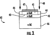
図3は、本発明の実施形態に係る接合部規定方法の全体的な模式図である。この方法は、模式的に矢印40で表したイオンを、全体的に42で示すダイオード内の、p−n接合部43に隣接するエピタキシャル層41内にインプラントする(打ち込む)ことから成る。エピタキシャル層41は、第1導電型(図3ではp型として示す)を有する。インプラントするイオンの型及び量によって、インプラント領域44の固有抵抗が増大し、インプラント領域44を高抵抗性及び/又は半絶縁性にすることができる。これに関連して、「高抵抗性」とは、物質が十分に抵抗性となり、ウェハ上の隣接するダイのアノードに電圧バイアスを印加したときに、無視し得る電流しか流れないようになることを意味する。即ち、インプラント領域44における物質は、実質的に電気的に隣接するダイを隔離する場合、本発明の目的上、高抵抗性であると見なされる。実施形態の中には、インプラント領域44の固有抵抗が少なくとも2000Ω−cmである場合もある。物質の固有抵抗が十分に高い場合、この物質は、p型又はn型半導体材料ではなく、半絶縁(又は「i型」)材料と見なすことができる。一般に、常温において1×105Ω−cmを超える固有抵抗を有する材料は、本発明の主旨から、半絶縁性と見なすことができる。
FIG. 3 is an overall schematic diagram of the joint defining method according to the embodiment of the present invention. This method consists of implanting (implanting) ions, schematically represented by
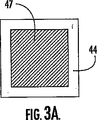
イオン40は、パターン状にインプラントされ、図3Aに更に明確に示すような、インプラントされた周囲44を規定することができる。該周囲44には、高抵抗性となるようにインプラントされたイオン40が十分にドープされており、これによってインプラントされた周囲44によって接合部43をアイソレート即ち隔離規定することができる。また、図3は、n型層45、基板46、及び金属接点47も示す。また、エピタキシャル層41における斜線は、図3の構造における周囲の位置を示している。
The
実施形態の中には、基板46が、2H、4H、6H、8H、15R、及び3Cポリタイプの炭化珪素から成る群から選択したポリタイプを有するn型炭化珪素で構成したものもある。しかしながら、当業者には認められようが、基板46は、サファイア、窒化ガリウムのようなその他の材料、あるいはMgO、スピネル、又はZnOのようなその他の適した材料で構成することも可能である。更に、基板46を導電性にすれば、縦型素子の形成が可能となり、あるいは基板46を絶縁性又は半絶縁性にすることもできる。
In some embodiments, the
本発明の実施形態の中には、イオン40を素子内にインプラントする際の打ち込みマスクとして、金属接点47を使用することができるものもある。例えば、金属接点47が、イオン40が層41に達するのを防止する程十分な厚さを有する金属スタックで構成される場合、別個のインプラント・マスクを堆積することを回避できる場合もある。
In some embodiments of the present invention, the
図3において模式的に示すように、一実施形態では、本方法は、窒素又は燐のようなイオンをp型窒化ガリウム層にインプラントすることを含む。水素、ヘリウム、アルミニウム、及びN2を含む他のイオンを用いると、インプラントによって領域の固有抵抗を高めることができる。本方法の他の面については、図5に関して示すことにする。 As shown schematically in FIG. 3, in one embodiment, the method includes implanting ions such as nitrogen or phosphorus into the p-type gallium nitride layer. Hydrogen, helium, when using aluminum, and other ions including N 2, it is possible to increase the resistivity of the region by the implant. Other aspects of the method will be described with respect to FIG.
インプラントは、従来通りに常温にて行うことができる。現在最良に理解されているところでは(そして、特定の理論によって限定されないとする)、イオンをインプラントすることによってGaN内に損傷が発生し、バンドギャップ内に深いレベルが生ずる。一方、これらは、GaN内の自由キャリアを捕獲し、これによって材料を高抵抗性にする。 The implant can be performed at room temperature as usual. Currently best understood (and not limited by any particular theory), implanting ions causes damage in the GaN, resulting in deep levels in the band gap. On the other hand, they capture free carriers in GaN, thereby making the material highly resistive.
GaNのようなIII群窒化物の発光ダイオードは、n型基板及びp型最上層の使用に限定される訳ではない。しかしながら、何故一般にSiC基板の方が多く用いられているかについては、多数の理由が有り、当技術分野ではよく理解されている。つまり、本発明もn型層にインプラントを行い、その固有抵抗を高めることができる。しかしながら、n型基板の使用の方が一般的であるので、本明細書における説明の殆どは、そのような構造に言及している。 Group III nitride light emitting diodes such as GaN are not limited to the use of n-type substrates and p-type top layers. However, there are many reasons why SiC substrates are generally used more often and are well understood in the art. That is, the present invention can also implant the n-type layer and increase its specific resistance. However, since the use of n-type substrates is more common, most of the description herein refers to such structures.
2層(n型及びp型)の窒化ガリウム層を組み込んだ発光ダイオードを示すが、ダイオード42は、1つ以上の量子ウエル、又は超格子構造、あるいはその双方を含むことができること、そして1つ又は複数の活性層は窒化ガリウムのみの場合よりも広い範囲のIII群窒化化合物を含むことができることは、当業者には認められよう。しかしながら、これらの変形は、本発明を明確に理解するためには、詳しく述べる必要はなく、したがって、ここではこれらについては詳しく論じない。よって、更に精巧な素子の関連部分も、「活性層」、「ダイオード部分」、「ダイオード領域」、又は「ダイオード構造」と呼んでもよく、本発明の範囲から逸脱することはない。
Although a light emitting diode incorporating a bilayer (n-type and p-type) gallium nitride layer is shown, the
図4は、図1と同様の模式断面図であるが、本発明の打ち込み周囲領域54を組み込み、全体的に50で示すダイオードを示す。ダイオード50は、基板51を含み、多くの実施形態では、これはn型炭化珪素である。
基板51上にn型窒化ガリウム・エピタキシャル層があり、図4に示す「フリップ・チップ」配位で基板51直下に見られる。p型層53がn型層52に隣接し、これら2つの層が、それらの間にp−n接合部58を規定する。このダイオードは、オーミック・コンタクト55、及びダイ取付金属部56も含む。
FIG. 4 is a schematic cross-sectional view similar to FIG. 1, but showing a diode generally indicated at 50, incorporating the implant peripheral region 54 of the present invention. The diode 50 includes a
There is an n-type gallium nitride epitaxial layer on the
図3に関して説明したような様式でインプラントが行われたので、ダイオードは、図4において点線に隣接して示す、高抵抗周囲部分54を含む。理想的に配置されていないダイ取付金属60の部分54も、リード・フレーム57上に示す。このように図示すると、本発明の様々な進展が見られる。第1に、金属部分60に利用可能な幾何学的空間面積は、ここでは一層制限されている。何故なら、ダイオード50のインプラントされた領域54は、メサを形成するために必要な多数の工程を必要としないからである。このため、p型層及びその絶縁部分54が、過剰金属の幾何学的空間阻止を強化する。加えて、インプラントされた部分54は非常に抵抗が高いので、過剰金属60とインプラントされた周囲部分54との間には、電気的相互作用が殆ど又は全くない。最後に、n型エピタキシャル層52に達するためには必要となる、望ましくない過剰金属60の量は遥かに多い。別の言い方をすると、本発明は、標準的な又は規定された量のダイ取付金属56、60を用いる場合、誤差に対する許容範囲を拡大することができる。先に図1に関して注記したように、動作及び実施上では、ダイオード50は、リード・フレームに対してアノード及びカソードの双方が接続するが、本発明の例示を明確化するために、これらの接続の詳細は除外してある。
Since the implant was performed in the manner described with respect to FIG. 3, the diode includes a high resistance peripheral portion 54, shown adjacent to the dotted line in FIG. A portion 54 of die attach
更に本発明の更なる詳細の一部について、基板51は、導電性炭化珪素で形成したものとして図4に示したが、半絶縁炭化珪素又は(絶縁体である)サファイアで構成することもできる。これは、本発明の利点が、エピタキシャル層において得られる利点に基づくからである。このため、絶縁又は半絶縁基板は、パッケージングのためには、導電性SiC基板とは多少異なる外形寸法を必要とするが、本発明及びエピタキシャル層に関する原理は同一のままである。更に、発光ダイオードでは、基板51は、電位差を素子に印加したときに接合部58が放出する光に対して、実質的に透過性であることが好ましい。炭化珪素は可視スペクトルのエネルギが高い方の部分において発光するので、基板は、約390〜550ナノメートルの間の波長を有する光に対して実質的に透過性であることが好ましく、更に好ましくは、約485〜550ナノメートルの間である。米国特許第5,718,7609号並びにその関連特許第6,025,289号及び第6,200,917号は、無色のSiCを生産する技術について記載している。これらの特許は、本発明と同じ譲受人に譲渡されており、ここで引用したことにより、その全体が本願にも含まれるものとする。
Further, for some of the further details of the present invention, the
前述のように、半絶縁境界部分54は、境界54がn型である場合にはショットキー挙動を生ずる金属と境界54が接触しているときも、ショットキー挙動を排除するのに十分な固有抵抗を有する。 As described above, the semi-insulating boundary portion 54 is unique enough to eliminate Schottky behavior even when the boundary 54 is in contact with a metal that produces Schottky behavior when the boundary 54 is n-type. Has resistance.
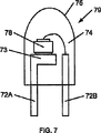
図7に示すように、本発明及び図3又は図4に示した種類の発光ダイオード78は、パッケージ内に実装することができる。パッケージは、ヘッダ73、電気リード72、及び封止材74(エポキシ等)を備えており、封止材74はレンズ75の形状に成形することができる。LED78は、従来の基板下方配位、又はエピタキシャル層がヘッダ73に隣接する「フリップ・チップ」配位で実装することができる。その結果、LEDランプ79は、ディスプレイの一部として組み込むことができ、指示光、バックライト、又はその他の用途として用いることができる。
As shown in FIG. 7, the
p型層へのオーミック・コンタクトは、通常、プラチナ、ニッケル、金、チタン、アルミニウム、銀、及びこれらの組み合わせから成る群から選択され、炭化珪素基板に対してオーミック・コンタクトを構成する場合、大抵の場合、ニッケル、プラチナ、パラディウム、アルミニウム、チタン、及びその組み合わせから成る群から選択される。基板に対するオーミック・コンタクト(図4には示されていない)は、光が放出することが望ましい方向に、見えるように配置するので、そして接点が大きい程電流拡散の利点があるので、オーミック・コンタクトとして、できるだけ透明に近いものを選択し形成することが好ましく、通常、該当する回路への電流の流れを増大させるために、更に小さい追加パッドを付加する。 The ohmic contact to the p-type layer is usually selected from the group consisting of platinum, nickel, gold, titanium, aluminum, silver, and combinations thereof, and is often the case when forming an ohmic contact to a silicon carbide substrate. , Selected from the group consisting of nickel, platinum, palladium, aluminum, titanium, and combinations thereof. The ohmic contact to the substrate (not shown in FIG. 4) is positioned so that it can be seen in the direction in which light is desired to be emitted, and the larger the contact, the more current spreading advantages, so the ohmic contact In order to increase the current flow to the corresponding circuit, it is usually preferable to add a smaller additional pad.
同様に、オーミック・コンタクト55及びダイ取付金属56は、ミラー又は反射体として作用し、ダイオード50がパッケージ化され使用されるときに、ダイオード50の最終的な出力を高めるように選択することができる。あるいは、この目的のために、追加の金属層(又は複数の層)を含ませることができる。更に、汚染物の拡散を防止するためのバリア層や、外部接点を素子に接合するための接合層のように、他の目的のために他の金属層を金属スタックに含めてもよい。
Similarly,
素子の基本的な図に関して、そして前述の方法に関して先に注記したように、本発明の構造は、図4の模式図に限定される訳ではない。多数の理由により、バッファ層は、構造の一部として、炭化珪素基板と第1窒化ガリウム(又はその他のIII群窒化物)層との間に含まれることが多い。多くの場合、バッファ層は、窒化アルミニウム、又は炭化珪素基板付近におけるより高いアルミニウム濃度から、窒化ガリウム・エピタキシャル層との界面におけるより高い窒化ガリウム濃度まで遷移する窒化アルミニウム・ガリウム(AlGaN)の漸変層で構成することができる。この種のダイオードに組み込むことができ、本発明が特に適している他の構造的部分は、素子の結晶全体の安定性を高めるための超格子構造、光の出力を高めるか又はそれを特定の周波数に同調させるための量子ウエル、あるいは活性層の層数を追加しそれらの間の関係を定めることによって素子の明るさを高めるための多数の量子井ウエルを含む。加えて、環境保護のために、素子50のエピタキシャル層52、53の露出面を不動態化すなわちパッシベートすることが望ましいこともある。前述のように、このような不動態化は、PECVD、スパッタリング、又はその他の適した不動態化技術によって堆積する二酸化シリコン又は窒化シリコンで構成することができる。
As noted above with respect to the basic diagram of the device and with respect to the foregoing method, the structure of the present invention is not limited to the schematic diagram of FIG. For a number of reasons, the buffer layer is often included as part of the structure between the silicon carbide substrate and the first gallium nitride (or other group III nitride) layer. In many cases, the buffer layer is a gradual change in aluminum gallium nitride (AlGaN) that transitions from a higher aluminum concentration near the aluminum nitride or silicon carbide substrate to a higher gallium nitride concentration at the interface with the gallium nitride epitaxial layer. Can be composed of layers. Other structural parts that can be incorporated into this type of diode and are particularly suitable for the present invention are superlattice structures to increase the stability of the entire crystal of the device, increase the light output or make it specific It includes a quantum well for tuning to the frequency, or a number of quantum wells for increasing the brightness of the device by adding the number of active layers and defining the relationship between them. In addition, it may be desirable to passivate or passivate the exposed surfaces of the
図5は、本発明の方法の態様の一部を示す。広義な意味では、本方法は、ダイオードにおいて、最も好ましくはIII群窒化物又は窒化ガリウム系ダイオードにおいて、ダイオードを使用のために実装するときの望ましくない電気的接触及び経路を最小限に止めるか又は回避するため、及び/又はダイ分離中におけるp−n接合部への損傷を防止するために、p−n接合部を電気的に規定又は隔離する。この態様では、本方法は、p−n接合部の一部である窒化ガリウムのp型エピタキシャル層の中央部分上にオーミック金属コンタクト層を形成し、この金属層上にエッチング・マスクを配することによって該金属層のパターニングを行い、エッチング・マスク及び金属層の一部を除去し、次いでエッチング・マスクによって被覆されていないp型エピタキシャル層の周囲部分にイオンを打ち込むことから成る。 FIG. 5 illustrates some of the method aspects of the present invention. In a broad sense, the method minimizes undesirable electrical contacts and paths when mounting a diode for use in a diode, most preferably a Group III nitride or gallium nitride based diode, or To avoid and / or prevent damage to the pn junction during die separation, the pn junction is electrically defined or isolated. In this aspect, the method forms an ohmic metal contact layer on a central portion of a p-type epitaxial layer of gallium nitride that is part of a pn junction and places an etching mask on the metal layer. Patterning the metal layer, removing the etching mask and a portion of the metal layer, and then implanting ions into the surrounding portion of the p-type epitaxial layer not covered by the etching mask.
更に態様を多少詳しく述べると、本方法は、オーミック金属層(及び潜在的にオーミック・コンタクト上の接合パッド)の一部にマスキングを施し、残りの露出したオーミック金属コンタクト層をエピタキシャル層から除去し、露出部分の固有抵抗を高めるのに十分な原子をエピタキシャル層の露出部分にインプラントし(そして潜在的に露出部分を半絶縁性にし)、オーミック・コンタクト(及び接合パッド)からマスクを除去することによって、p型層の高固有抵抗部分を形成する。この態様では、本方法は、マスキング工程の前にオーミック・コンタクト及び接合パッドを形成し、オーミック・コンタクト金属にフォトレジストでマスキングを施すことを含むことができる。 To further elaborate, the method masks a portion of the ohmic metal layer (and potentially the bonding pad on the ohmic contact) and removes the remaining exposed ohmic metal contact layer from the epitaxial layer. Implanting enough atoms into the exposed portion of the epitaxial layer (and potentially making the exposed portion semi-insulating) to remove the mask from the ohmic contact (and bond pad), to increase the resistivity of the exposed portion Thus, the high resistivity portion of the p-type layer is formed. In this aspect, the method can include forming ohmic contacts and bond pads prior to the masking step and masking the ohmic contact metal with a photoresist.
図5に戻って更に詳細に説明すると、全体的に60で示すデバイス先駆体が示されている。ダイオード先駆体60は、基板61(ある実施形態では、n型SiCで構成する)、基板61上にあるn型窒化ガリウム・エピタキシャル層62、n型層62上にあるp型窒化ガリウム・エピタキシャル層63、p型層63上にあるオーミック・コンタクト層65、及びオーミック・コンタクト層65上にある金属接合パッド66を含む。基板及びエピタキシャル層を形成し、オーミック・コンタクト及び接合パッドを形成する種々の工程は、一般に当技術分野では周知であり、ここでは詳細に説明しない。代表的な記載は、本願と同じ譲受人に譲渡された、発行済みの米国特許第6,297,522号、第6,217,662号、第6,063,186号、第5,679,153号、第5,393,993号、及び第5,119,540号に含まれるが、これらに限定されるのではない。
Returning to FIG. 5, in further detail, a device precursor generally indicated at 60 is shown. The
図5の(B)は、フォトレジストを堆積し、マスキングし、パターニングして、図5の(B)に示すように、フォトレジスト部分67を接合パッド全て、そしてオーミック・コンタクト65の一部であるが全てではないエリアの上に形成した後のダイオード先駆体60を示す。次に、図5の(B)の先駆体をエッチングして、フォトレジスト67によって被覆されていないオーミック・コンタクト層65の部分を除去する。このエッチングは、しかるべき様式であれば任意のもので行うこともできるが、塩素系プラズマを用いた反応性イオン・エッチング(RIE)が1つの可能な方法である。このエッチングによって、図5の(C)に示す構造が得られ、オーミック・コンタクトのサイズが、65(a)で表される面積に縮小されている。また、図5の(C)は、オーミック・コンタクト層65の一部を除去したため、p型エピタキシャル窒化ガリウム層の一部が露出していることも示す。
FIG. 5 (B) shows that photoresist is deposited, masked, and patterned to place the
次に、図5の(D)は、接合部64を規定し隔離するp型窒化ガリウム層63における高抵抗領域71を形成するためのイオン70のインプラントを(模式的に)示す。実施形態の中には、高抵抗のインプラントされた領域71が半絶縁性となるものもある。
あるいは、図5の(D)に示す打ち込み工程は、オーミック・コンタクト層65が十分に薄く、打ち込み工程を実質的に妨害しないのであれば、オーミック・コンタクト層65をエッチングする工程の前に実施してもよい。
Next, FIG. 5D shows (schematically) an implant of
Alternatively, the implantation step shown in FIG. 5D is performed before the step of etching the ohmic contact layer 65 if the ohmic contact layer 65 is sufficiently thin and does not substantially interfere with the implantation step. May be.
フォトレジスト67を除去すると、図5の(E)に示す先駆体構造が得られる。次いで、先駆体構造を個々のダイに分離することができる。
フォトレジスト67は2工程(オーミック・コンタクト層65をエッチングし、イオン70をインプラントする)のマスクとして機能するので、本発明の方法は、製作サイクル時間、ウェハ処理及び薬品消費を削減し、同様に、他の場合にはマスキング及びエッチング手順に伴う歩留まりの損失を低減する。
When the
Since the
本発明の別の実施形態を図6の(A)〜図6の(D)に示す。この実施形態では、基板81と、エピタキシャル領域82及び83を備えたウェハ80を用意する。図6の(A)に示すように、エピタキシャル領域83上に金属スタック86を形成する。先に論じたように、エピタキシャル領域83は第1導電型を有し、エピタキシャル領域82は第1導電型とは逆の第2導電型を有する。エピタキシャル領域82及び83の各々は、同じ導電型の1つ以上の層で構成することができる。金属スタック86は、多数の金属層で構成することができ、その各々は特定の機能を有する。例えば、金属スタック86は、エピタキシャル領域83とオーミック・コンタクトを形成する金属層を備えることができる。また、金属スタック86は、反射体、バリア、接着層、接合層、及び/又はその他の層も備えることができる。
Another embodiment of the present invention is shown in FIGS. 6A to 6D. In this embodiment, a
図6の(B)に示すように、金属スタック86上にエッチング・マスク85を形成し、フォトリソグラフィによってパターニングして開口を形成し、金属スタック86の表面部分86Aを選択的に露呈させる。あるいは、金属スタック86は、フォトリソグラフィ、デポジット、及びリフトオフ技術によって形成することができる。これらは当技術分野では周知である。即ち、金属スタック86は、ブランケット・フォトレジストをエピタキシャル領域83の表面に配し、これを露光し現像することによってフォトレジストをパターニングし、金属をブランケット層として堆積し、不要な金属を剥離することによって、形成することができる。
As shown in FIG. 6B, an
これより図6の(C)に移ると、金属スタック86を選択的にエッチングし、エピタキシャル領域83の表面部分83Aを露呈させる。次いで、従来の方法でエッチング・マスク85を除去する。次に、エピタキシャル領域83の露出部分にイオン87をインプラントし、前述のように、インプラント領域84を高抵抗性とし、構造内にp−n接合領域88を規定する。この実施形態では、パターニングした金属層86がインプラント・マスクとして機能する。
6C, the
最後に、図6の(D)に示すように、エッチング/インプラント・マスク85を除去し、規定したp−n接合領域88がダイの側壁90から離間し、これによって物理的及び電気的に隔離するように、従来の技法を用いて個々のダイ89に分離する。
Finally, as shown in FIG. 6D, the etch /
実験結果
本発明を評価するに当たり、以下のインプラント手順を実行した。
以下の評価の各々において、n型炭化珪素基板、n型エピタキシャル領域、及びp型エピタキシャル領域を備えたLED先駆体を用意した。p型エピタキシャル領域は、キャリア濃度が約1〜5×1017cm−3のMgをドープしたGaN/AlGaNから成り、厚さの合計は約210nmであった。第1の評価において、1平方センチメートル当たり1013の投与量(cm−2)の一価窒素(N+1)を20keVで、1.4×1013cm−2の投与量のN+1を125keVで、そして2×1013cm−2の投与量の二価窒素(N+2)を125keVで、連続投与を実行した。
Experimental Results In evaluating the present invention, the following implant procedure was performed.
In each of the following evaluations, an LED precursor including an n-type silicon carbide substrate, an n-type epitaxial region, and a p-type epitaxial region was prepared. The p-type epitaxial region was made of GaN / AlGaN doped with Mg having a carrier concentration of about 1 to 5 × 10 17 cm −3 , and the total thickness was about 210 nm. In the first evaluation, 10 13 doses per square centimeter (cm −2 ) monovalent nitrogen (N +1 ) at 20 keV, 1.4 × 10 13 cm −2 dose N +1 at 125 keV, Then, continuous administration was performed at 125 keV with 2 × 10 13 cm −2 dose of divalent nitrogen (N +2 ).
第2の評価において、1013cm−2の投与量のN+1窒素を20keVで打ち込み、続いて、1.4×1013cm−2において一価窒素を125keVで投与した。
第3の評価において、1013cm−2の投与量でN+1を用いて、最初の投与を20keVで実行し、続いて1.4×1013cm−2の投与量及び125keVで投与し、その後に1.7×1013cm−2のN+1を190keVで投与した。
In the second evaluation, a dose of 10 13 cm −2 of N + 1 nitrogen was implanted at 20 keV, followed by administration of monovalent nitrogen at 125 keV at 1.4 × 10 13 cm −2 .
In a third evaluation, with N + 1 at a dose of 10 13 cm −2 , the first dose is performed at 20 keV, followed by a dose of 1.4 × 10 13 cm −2 and 125 keV, Thereafter, 1.7 × 10 13 cm −2 of N + 1 was administered at 190 keV.
以上3つの条件では、全てで接合部の隔離及び規定が得られた。接合部の隔離を検証する際、隣接する金属スタックを探針で調べ、連続性の測定を行った。p−n接合部の破壊以前には、測定可能な電流は観察されなかった。インプラントしたヘリウム及び窒素は抵抗性条件も生じさせ、常温において殆ど任意のイオンをp型窒化ガリウムにインプラントしても、物質は劇的に抵抗性が高くなるという、予想されていた結論に至った。
しかしながら、本発明者はいずれの特定的な理論にも縛られることを望んでいない。したがって、予想されていた結論についてここで論じたのは、限定ではなく例示のために行ったのである。
Under the above three conditions, isolation and regulation of the joint were obtained in all. When verifying the separation of the joints, adjacent metal stacks were examined with a probe to measure continuity. Prior to the breakdown of the pn junction, no measurable current was observed. Implanted helium and nitrogen also create a resistance condition, leading to the expected conclusion that even if almost any ion is implanted into p-type gallium nitride at room temperature, the material is dramatically more resistant. .
However, the inventor does not want to be bound by any particular theory. Therefore, the discussion of the expected conclusions has been made here for purposes of illustration and not limitation.
これらのインプラント工程により、接合部の端縁は、絶縁性で不活性(要望により)となる。また、インプラント工程は、p型窒化ガリウムが表明した低ホール濃度(約1×1017cm−3)のために、p型窒化ガリウムにも適している。本発明の打ち込みによって生じた不活性特性は、900℃付近の温度まで安定であると思われる。したがって、この技法による接合部の隔離は、p型層を組み込んだいずれの窒化物素子にも適していると思われる。この理由のため、サファイア上ならびに炭化珪素及びその他の基板上の窒化物系発光ダイオードは、接合部の隔離用の打ち込みの使用により、等しく効果が得られると思われる。 With these implant steps, the edge of the joint becomes insulating and inert (if desired). The implant process is also suitable for p-type gallium nitride because of the low hole concentration (about 1 × 10 17 cm −3 ) expressed by p-type gallium nitride. The inert properties produced by the implantation of the present invention appear to be stable up to temperatures around 900 ° C. Therefore, junction isolation by this technique appears to be suitable for any nitride device incorporating a p-type layer. For this reason, nitride-based light emitting diodes on sapphire and on silicon carbide and other substrates would be equally effective with the use of junction isolation implants.
Cree Inc.から市販されているダイに対して、以下の評価を行った。
標準的なインプラント条件は、以下の(1)の通りであった。他の条件(2)〜(5)も試験した。(2)の条件は、インプラントしたイオン当たりの排除したキャリア数を評価することを意図した。条件(3)及び(5)は、素子のp側のみに打ち込みを行う効果を評価することを意図した。条件(4)は、(1)及び(2)の比較と同様、キャリアを捕獲する効率を評価した。インプラントを行う際、Cree社の緑色LEDには、Cree社の青色LEDに比較して、高いエネルギがインプラントに必要であることが判明した。
The following evaluation was performed on a die commercially available from Cree Inc.
The standard implant conditions were as follows (1). Other conditions (2) to (5) were also tested. Condition (2) was intended to evaluate the number of excluded carriers per implanted ion. Conditions (3) and (5) were intended to evaluate the effect of implanting only on the p side of the device. Condition (4) evaluated the efficiency which capture | acquires a carrier similarly to the comparison of (1) and (2). When implanting, it was found that Cree green LEDs require higher energy for the implant compared to Cree blue LEDs.
青色に対して考察した打ち込み条件(連続投与を示す)
(1)1e13@20keV、1.4e13@125keV、1.7e13@190keV(標準的な三重投与条件)
(2)1e12@20keV、1.4e12@125keV、1.7e12@190keV(1/10投与における標準的な条件)
(3)1.4e13@125keV(#1の標準的条件の内1回の投与)
(4)1.4e12@125keV(#4の1/10の投与)
(5)1e13@30keV、1.4e13@100keV
Implantation conditions considered for blue (indicates continuous administration)
(1) 1e13 @ 20 keV, 1.4e13@125 keV, 1.7e13@190 keV (standard triple administration conditions)
(2) 1e12 @ 20 keV, 1.4e12@125 keV, 1.7e12@190 keV (standard conditions for 1/10 administration)
(3) 1.4e13@125 keV (one dose of standard conditions of # 1)
(4) 1.4e12@125 keV (1/10 administration of # 4)
(5) 1e13 @ 30 keV, 1.4e13@100 keV
Cree社の青色発光ダイオードについて、そしてTRIMシミュレーションに基づくと、条件(1)及び(2)の190keVでの打ち込みは、p−n接合部よりも遥か深くまで達し、190keVで打ち込んだ窒素の殆どがn側に行ってしまう。条件(3)及び(4)の125keVでの1回の投与、及び条件(5)の二重投与について検討した。100及び125keVのエネルギでは、窒素濃度のピークがp−n接合部又はその周囲に位置し、これは表面から1500〜1800A下方である。100及び125ekVでの打ち込みについてシミュレートしたピークは、それぞれ、1600及び2000Aである。GaN材料は、低抵抗性から高抵抗性に変換される。 For Cree blue light-emitting diodes and based on the TRIM simulation, the conditions (1) and (2) implant at 190 keV reach much deeper than the pn junction, and most of the nitrogen implanted at 190 keV Go to the n side. A single administration at 125 keV under conditions (3) and (4) and a double administration under condition (5) were studied. At energies of 100 and 125 keV, the nitrogen concentration peak is located at or around the pn junction, which is 1500-1800 A below the surface. The simulated peaks for implantation at 100 and 125 ekV are 1600 and 2000A, respectively. GaN materials are converted from low resistance to high resistance.
P型GaNの厚さは約1000〜1500Aであり、自由ホール濃度は約2〜5E17/cm3である。
P型AlGaNの厚さは約300Aであり、ホール濃度は約5〜20E16/cm3である。
条件(1)は、青色LEDに対しては常に有効である(即ち、所望の隔離及び静電放電(ESD)発生量)。
条件(2)では、素子の隔離は首尾良く行われるものの、ESD発生量が乏しい。
条件(3)では、素子が隔離され、ESD発生量も多い。
条件(4)では、素子は完全には隔離されず、ESD発生量も多くない。
条件(5)では、素子が隔離され、ESD発生量も多い。
The thickness of P-type GaN is about 1000-1500 A, and the free hole concentration is about 2-5E17 / cm 3 .
The thickness of P-type AlGaN is about 300 A, and the hole concentration is about 5 to 20E16 / cm 3 .
Condition (1) is always valid for blue LEDs (ie, desired isolation and electrostatic discharge (ESD) generation).
In the condition (2), although the element is successfully isolated, the amount of ESD generation is poor.
In condition (3), the element is isolated and the amount of ESD generated is large.
In the condition (4), the element is not completely isolated and the amount of ESD generation is not large.
In condition (5), the element is isolated and the amount of ESD generated is large.
Cree社の緑色発光ダイオードでは、条件(1)〜(5)の各々において、高抵抗p型材料が得られ、隣接する素子は隔離されたが、生じたESD発生量は多くなかった。しかしながら、2E13/cm2の投与量で更に230keVの窒素打ち込みを追加したところ、隔離及びESD発生量共に非常に有効であった。 In the green light emitting diode manufactured by Cree, a high resistance p-type material was obtained in each of the conditions (1) to (5), and adjacent elements were isolated, but the amount of generated ESD was not large. However, when 230 keV nitrogen implantation was further added at a dose of 2E13 / cm 2 , both sequestration and ESD generation were very effective.
生産再生プロセス(Production Recovery Process):他のデバイスには、製作後に不動態化を行った。この場合、デバイスには厚さ約1600Aの窒化シリコンを被覆した。青色に対する最良の条件は、前述の条件(1)に変わりないが、パシベーション層を貫通するために30keVの割り増しエネルギを要する。緑色LEDについても、2E13/cm2における追加の230keVでのインプラントにさらに割り増しの30keVを加えることによって、同様の結果が得られた。 Production Recovery Process: Other devices were passivated after production. In this case, the device was coated with about 1600 A thick silicon nitride. The best condition for blue is the same as condition (1) described above, but requires 30 keV of extra energy to penetrate the passivation layer. For even green LED, by adding more of the extra 30keV implant in additional 230keV in 2E13 / cm 2, similar results were obtained.
固有抵抗の推定:固有抵抗は、2×10³オーム−cmよりも大きいと推定した。これは、2ボルトの電圧を印加して2つの隣接するパッド間に流れる電流を評価することによって行った。得られた電流は測定不能であった(<50nA)。これは、40×106オームよりも大きい抵抗に対応する。パッド間の距離は、70ミクロンであり、幅は230ミクロンである。したがって、平方数(number of squares)は、これらの間で約0.3である。フリンジング効果を無視して、固有抵抗について最悪の場合の下限推定値を求めた。これによって、面抵抗に平方当たり133×106オームの下限が得られた。厚さを0.15×10⁻⁴cmの厚さにとると、2000オーム−cmよりも大きな固有抵抗が得られる。 Specific resistance estimation: The specific resistance was estimated to be greater than 2 × 10 3 ohm-cm. This was done by applying a voltage of 2 volts and evaluating the current flowing between two adjacent pads. The current obtained was not measurable (<50 nA). This corresponds to a resistance greater than 40 × 10 6 ohms. The distance between the pads is 70 microns and the width is 230 microns. Accordingly, the number of squares is about 0.3 between them. Ignoring the fringing effect, the lower limit estimated value in the worst case for the specific resistance was obtained. This resulted in a lower limit of sheet resistance of 133 × 10 6 ohms per square. If the thickness is 0.15 × 10 −4 cm, a resistivity greater than 2000 ohm-cm is obtained.
本発明の実施形態を図面及び明細書に明記した。特定的な用語を用いたが、これらは包括的及び記述的な意味で用いたに過ぎず、限定を目的としたのではない。本発明の範囲は、特許請求の範囲において規定されるものとする。 Embodiments of the present invention are specified in the drawings and specification. Although specific terms have been used, they have been used in a generic and descriptive sense only and not for purposes of limitation. The scope of the invention is to be defined in the claims.
Claims (10)
第1導電型を有するIII族窒化物の第1エピタキシャル領域と、
前記第1導電型とは反対の第2導電型を有し、前記第1エピタキシャル領域上にあるIII族窒化物の第2エピタキシャル領域であって、前記第1エピタキシャル領域と共にpn接合部を形成する第2エピタキシャル領域と、
前記第2エピタキシャル領域と前記リード・フレームとの間に配置され、前記リード・フレームと前記第2エピタキシャル領域とを電気的に接続するオーミック・コンタクトであって、前記リード・フレームとの間にダイ取付金属が介在されているオーミック・コンタクトと、
前記第1エピタキシャル領域上にあり、前記第2エピタキシャル領域を包囲するIII族窒化物の隔離領域であって、前記pn接合部を前記リード・フレームから電気的に隔離するために前記第2エピタキシャル領域と比較して固有抵抗が増大されているIII族窒化物の隔離領域と
を備えており、前記オーミック・コンタクトは、反射層を含む金属スタックを含み、かつ、前記III族窒化物の隔離領域を露出した状態で前記第2エピタキシャル領域を画定する
ことを特徴とする発光ダイオード。A light emitting diode on a lead frame,
A first epitaxial region of a group III nitride having a first conductivity type;
A second conductivity region of a group III nitride having a second conductivity type opposite to the first conductivity type, and forming a pn junction together with the first epitaxial region; A second epitaxial region;
An ohmic contact disposed between the second epitaxial region and the lead frame and electrically connecting the lead frame and the second epitaxial region, wherein a die is interposed between the lead frame and the lead frame. Ohmic contact with mounting metal interposed,
A III-nitride isolation region overlying the first epitaxial region and surrounding the second epitaxial region, wherein the second epitaxial region is used to electrically isolate the pn junction from the lead frame A III-nitride isolation region having an increased resistivity as compared to the ohmic contact, wherein the ohmic contact includes a metal stack including a reflective layer, and the III-nitride isolation region A light emitting diode, wherein the second epitaxial region is defined in an exposed state.
基板と、
前記基板と前記第1エピタキシャル領域との間の前記基板上のバッファ層であって、前記第1及び第2エピタキシャル領域は、電流が流れると発光する活性構造の少なくとも一部をこのバッファ層上に形成する、バッファ層と、
前記活性構造の内にあるIII族窒化物のp型エピタキシャル層と、
前記発光ダイオードと前記活性構造とに電流を与え所望の発光を生じさせる前記発光ダイオードへの第2オーミック・コンタクトと
を備え、前記隔離領域は前記活性構造の内にあり前記p型エピタキシャル層を包囲し前記活性構造の一部を電気的に隔離する高抵抗窒化ガリウム境界を含むことを特徴とする半導体発光ダイオード。The light emitting diode according to claim 1.
A substrate,
A buffer layer on the substrate between the substrate and the first epitaxial region, wherein the first and second epitaxial regions have at least a part of an active structure that emits light when a current flows on the buffer layer. Forming a buffer layer;
A group III nitride p-type epitaxial layer in the active structure;
And a second ohmic contact to said light emitting diode to produce a desired light emission gives a current to the light emitting diode and the active structure, the isolation region surrounding the p-type epitaxial layer located within the active structure A semiconductor light emitting diode comprising a high resistance gallium nitride boundary that electrically isolates a portion of the active structure .
n型導電性の炭化シリコン基板を備えていて、
前記III族窒化物の第1エピタキシャル領域は、n型であり、
前記III族窒化物の第2エピタキシャル領域は、p型である
ことを特徴とする発光ダイオード。The light emitting diode according to claim 1.
an n-type conductive silicon carbide substrate,
The first epitaxial region of the group III nitride is n-type,
2. The light emitting diode according to claim 1, wherein the second epitaxial region of the group III nitride is p-type.
Applications Claiming Priority (3)
| Application Number | Priority Date | Filing Date | Title |
|---|---|---|---|
| US32018203P | 2003-05-09 | 2003-05-09 | |
| US60/320,182 | 2003-05-09 | ||
| PCT/US2004/014023 WO2004102686A1 (en) | 2003-05-09 | 2004-05-06 | Led fabrication via ion implant isolation |
Related Child Applications (1)
| Application Number | Title | Priority Date | Filing Date |
|---|---|---|---|
| JP2011056687A Division JP5491439B2 (en) | 2003-05-09 | 2011-03-15 | LED production by ion implant isolation |
Publications (3)
| Publication Number | Publication Date |
|---|---|
| JP2006528435A JP2006528435A (en) | 2006-12-14 |
| JP2006528435A5 JP2006528435A5 (en) | 2007-06-14 |
| JP5122817B2 true JP5122817B2 (en) | 2013-01-16 |
Family
ID=33449503
Family Applications (2)
| Application Number | Title | Priority Date | Filing Date |
|---|---|---|---|
| JP2006532792A Active JP5122817B2 (en) | 2003-05-09 | 2004-05-06 | LED production by ion implant isolation |
| JP2011056687A Active JP5491439B2 (en) | 2003-05-09 | 2011-03-15 | LED production by ion implant isolation |
Family Applications After (1)
| Application Number | Title | Priority Date | Filing Date |
|---|---|---|---|
| JP2011056687A Active JP5491439B2 (en) | 2003-05-09 | 2011-03-15 | LED production by ion implant isolation |
Country Status (6)
| Country | Link |
|---|---|
| US (1) | US7338822B2 (en) |
| EP (1) | EP1623467B1 (en) |
| JP (2) | JP5122817B2 (en) |
| CN (2) | CN101697366B (en) |
| TW (1) | TWI347683B (en) |
| WO (1) | WO2004102686A1 (en) |
Families Citing this family (45)
| Publication number | Priority date | Publication date | Assignee | Title |
|---|---|---|---|---|
| CN101697366B (en) * | 2003-05-09 | 2012-12-19 | 克里公司 | LED via ion implant isolation |
| JP4766845B2 (en) * | 2003-07-25 | 2011-09-07 | シャープ株式会社 | Nitride-based compound semiconductor light-emitting device and method for manufacturing the same |
| CN101335320B (en) * | 2003-09-19 | 2012-06-06 | 霆激科技股份有限公司 | Method for manufacturing light emitting device |
| CN100452328C (en) * | 2003-09-19 | 2009-01-14 | 霆激技术有限公司 | Fabrication of conductive metal layer on semiconductor devices |
| US20050194584A1 (en) * | 2003-11-12 | 2005-09-08 | Slater David B.Jr. | LED fabrication via ion implant isolation |
| JP2007535804A (en) * | 2004-03-15 | 2007-12-06 | ティンギ テクノロジーズ プライベート リミテッド | Semiconductor device manufacturing |
| CN1998094B (en) * | 2004-04-07 | 2012-12-26 | 霆激技术有限公司 | Fabrication of reflective layer on semiconductor light emitting diodes |
| US7592634B2 (en) * | 2004-05-06 | 2009-09-22 | Cree, Inc. | LED fabrication via ion implant isolation |
| US8174037B2 (en) | 2004-09-22 | 2012-05-08 | Cree, Inc. | High efficiency group III nitride LED with lenticular surface |
| SG130975A1 (en) * | 2005-09-29 | 2007-04-26 | Tinggi Tech Private Ltd | Fabrication of semiconductor devices for light emission |
| SG131803A1 (en) | 2005-10-19 | 2007-05-28 | Tinggi Tech Private Ltd | Fabrication of transistors |
| SG133432A1 (en) * | 2005-12-20 | 2007-07-30 | Tinggi Tech Private Ltd | Localized annealing during semiconductor device fabrication |
| KR20080106402A (en) | 2006-01-05 | 2008-12-05 | 일루미텍스, 인크. | Separate optical device for directing light from an led |
| JP2008041811A (en) * | 2006-08-03 | 2008-02-21 | Ngk Spark Plug Co Ltd | Wiring circuit board, multiple-chip wiring circuit board, and method for manufacturing the wiring board |
| SG140473A1 (en) | 2006-08-16 | 2008-03-28 | Tinggi Tech Private Ltd | Improvements in external light efficiency of light emitting diodes |
| US7646024B2 (en) * | 2006-08-18 | 2010-01-12 | Cree, Inc. | Structure and method for reducing forward voltage across a silicon carbide-group III nitride interface |
| SG140512A1 (en) | 2006-09-04 | 2008-03-28 | Tinggi Tech Private Ltd | Electrical current distribution in light emitting devices |
| EP2070123A2 (en) | 2006-10-02 | 2009-06-17 | Illumitex, Inc. | Led system and method |
| US8674593B2 (en) * | 2007-05-31 | 2014-03-18 | Nthdegree Technologies Worldwide Inc | Diode for a printable composition |
| EP2240968A1 (en) | 2008-02-08 | 2010-10-20 | Illumitex, Inc. | System and method for emitter layer shaping |
| US20090261346A1 (en) * | 2008-04-16 | 2009-10-22 | Ding-Yuan Chen | Integrating CMOS and Optical Devices on a Same Chip |
| TW201034256A (en) | 2008-12-11 | 2010-09-16 | Illumitex Inc | Systems and methods for packaging light-emitting diode devices |
| JP2010199558A (en) * | 2009-01-27 | 2010-09-09 | Panasonic Corp | Semiconductor device and method of manufacturing the same |
| US8096671B1 (en) | 2009-04-06 | 2012-01-17 | Nmera, Llc | Light emitting diode illumination system |
| US8449128B2 (en) | 2009-08-20 | 2013-05-28 | Illumitex, Inc. | System and method for a lens and phosphor layer |
| US8585253B2 (en) | 2009-08-20 | 2013-11-19 | Illumitex, Inc. | System and method for color mixing lens array |
| US8263422B2 (en) | 2010-04-26 | 2012-09-11 | Varian Semiconductor Equipment Associates, Inc. | Bond pad isolation and current confinement in an LED using ion implantation |
| DE102010026518A1 (en) * | 2010-07-08 | 2012-01-12 | Osram Opto Semiconductors Gmbh | Light-emitting diode chip and method for producing a light-emitting diode chip |
| KR101782081B1 (en) * | 2010-08-30 | 2017-09-26 | 엘지이노텍 주식회사 | Light emitting device |
| US20120097918A1 (en) * | 2010-10-20 | 2012-04-26 | Varian Semiconductor Equipment Associates, Inc. | Implanted current confinement structure to improve current spreading |
| US8664027B2 (en) | 2011-02-11 | 2014-03-04 | Varian Semiconductor Associates, Inc. | LED mesa sidewall isolation by ion implantation |
| US8927999B2 (en) * | 2011-11-21 | 2015-01-06 | Avogy, Inc. | Edge termination by ion implantation in GaN |
| DE102012108883A1 (en) * | 2012-09-20 | 2014-03-20 | Osram Opto Semiconductors Gmbh | Optoelectronic semiconductor chip and method for producing optoelectronic semiconductor chips |
| TWI495154B (en) * | 2012-12-06 | 2015-08-01 | Genesis Photonics Inc | Semiconductor structure |
| US9985190B2 (en) * | 2016-05-18 | 2018-05-29 | eLux Inc. | Formation and structure of post enhanced diodes for orientation control |
| CN106711301B (en) * | 2015-11-12 | 2020-10-27 | 美科米尚技术有限公司 | Light emitting diode and manufacturing method thereof |
| CN106024623B (en) * | 2016-06-29 | 2019-03-01 | 江苏能华微电子科技发展有限公司 | A kind of gallium nitride Schottky diode and preparation method thereof |
| TWI703726B (en) | 2016-09-19 | 2020-09-01 | 新世紀光電股份有限公司 | Semiconductor device containing nitrogen |
| US10892137B2 (en) * | 2018-09-12 | 2021-01-12 | Entegris, Inc. | Ion implantation processes and apparatus using gallium |
| DE102019129619A1 (en) * | 2019-11-04 | 2021-05-06 | OSRAM Opto Semiconductors Gesellschaft mit beschränkter Haftung | OPTOELECTRONIC SEMI-CONDUCTOR COMPONENT |
| GB2590450B (en) * | 2019-12-18 | 2022-01-05 | Plessey Semiconductors Ltd | Light emitting diode precursor |
| CN111653565B (en) * | 2020-03-11 | 2023-03-17 | 厦门市三安集成电路有限公司 | High-impedance semiconductor resistor structure and preparation method thereof |
| US11227801B2 (en) | 2020-03-19 | 2022-01-18 | International Business Machines Corporation | Formation of contacts for semiconductor devices |
| CN114141916B (en) * | 2021-11-24 | 2023-08-01 | 福州大学 | Nanometer-sized LED chip array and preparation method thereof |
| CN114628432B (en) * | 2022-02-28 | 2023-03-10 | 诺视科技(苏州)有限公司 | Manufacturing method of semiconductor device and semiconductor device |
Family Cites Families (44)
| Publication number | Priority date | Publication date | Assignee | Title |
|---|---|---|---|---|
| BE791929A (en) | 1971-12-02 | 1973-03-16 | Western Electric Co | PROCESS FOR MANUFACTURING INSULATING REGIONS IN A SEMICONDUCTOR BODY |
| US4968582A (en) | 1988-06-28 | 1990-11-06 | Mcnc And University Of Nc At Charlotte | Photoresists resistant to oxygen plasmas |
| US5114827A (en) | 1988-06-28 | 1992-05-19 | Microelectronics Center Of N.C. | Photoresists resistant to oxygen plasmas |
| US5119540A (en) | 1990-07-24 | 1992-06-09 | Cree Research, Inc. | Apparatus for eliminating residual nitrogen contamination in epitaxial layers of silicon carbide and resulting product |
| JPH0394481A (en) * | 1989-09-07 | 1991-04-19 | Ricoh Co Ltd | Array-shaped semiconductor light-emitting device |
| US5210051A (en) * | 1990-03-27 | 1993-05-11 | Cree Research, Inc. | High efficiency light emitting diodes from bipolar gallium nitride |
| US5248760A (en) | 1991-01-25 | 1993-09-28 | Unc At Charlotte | Chemically cured low temperature polyimides |
| JPH0546052U (en) * | 1991-11-19 | 1993-06-18 | 三洋電機株式会社 | Light emitting diode device |
| JPH0697498A (en) * | 1992-09-17 | 1994-04-08 | Toshiba Corp | Semiconductor light emitting element |
| US5393642A (en) | 1992-12-31 | 1995-02-28 | The University Of North Carolina At Charlotte | Ionic modification of organic resins and photoresists to produce photoactive etch resistant compositions |
| US5416342A (en) | 1993-06-23 | 1995-05-16 | Cree Research, Inc. | Blue light-emitting diode with high external quantum efficiency |
| US5393993A (en) | 1993-12-13 | 1995-02-28 | Cree Research, Inc. | Buffer structure between silicon carbide and gallium nitride and resulting semiconductor devices |
| US5449925A (en) * | 1994-05-04 | 1995-09-12 | North Carolina State University | Voltage breakdown resistant monocrystalline silicon carbide semiconductor devices |
| US5592501A (en) | 1994-09-20 | 1997-01-07 | Cree Research, Inc. | Low-strain laser structures with group III nitride active layers |
| US5631190A (en) | 1994-10-07 | 1997-05-20 | Cree Research, Inc. | Method for producing high efficiency light-emitting diodes and resulting diode structures |
| US5679153A (en) | 1994-11-30 | 1997-10-21 | Cree Research, Inc. | Method for reducing micropipe formation in the epitaxial growth of silicon carbide and resulting silicon carbide structures |
| SE9500146D0 (en) | 1995-01-18 | 1995-01-18 | Abb Research Ltd | Semiconductor component in silicon carbide |
| US5718760A (en) | 1996-02-05 | 1998-02-17 | Cree Research, Inc. | Growth of colorless silicon carbide crystals |
| JP3688843B2 (en) | 1996-09-06 | 2005-08-31 | 株式会社東芝 | Nitride semiconductor device manufacturing method |
| US5866925A (en) | 1997-01-09 | 1999-02-02 | Sandia Corporation | Gallium nitride junction field-effect transistor |
| US6217662B1 (en) | 1997-03-24 | 2001-04-17 | Cree, Inc. | Susceptor designs for silicon carbide thin films |
| JPH10294491A (en) * | 1997-04-22 | 1998-11-04 | Toshiba Corp | Semiconductor light-emitting element, manufacture thereof and light-emitting device |
| US6201262B1 (en) | 1997-10-07 | 2001-03-13 | Cree, Inc. | Group III nitride photonic devices on silicon carbide substrates with conductive buffer interlay structure |
| US6063186A (en) | 1997-12-17 | 2000-05-16 | Cree, Inc. | Growth of very uniform silicon carbide epitaxial layers |
| JP3516433B2 (en) * | 1997-12-19 | 2004-04-05 | 昭和電工株式会社 | Compound semiconductor light emitting device |
| US5998232A (en) | 1998-01-16 | 1999-12-07 | Implant Sciences Corporation | Planar technology for producing light-emitting devices |
| JPH11214800A (en) * | 1998-01-28 | 1999-08-06 | Sony Corp | Semiconductor device and manufacture thereof |
| US6090300A (en) | 1998-05-26 | 2000-07-18 | Xerox Corporation | Ion-implantation assisted wet chemical etching of III-V nitrides and alloys |
| JP2000077713A (en) * | 1998-08-27 | 2000-03-14 | Sanyo Electric Co Ltd | Semiconductor light-emitting element |
| US6459100B1 (en) | 1998-09-16 | 2002-10-01 | Cree, Inc. | Vertical geometry ingan LED |
| US6331450B1 (en) | 1998-12-22 | 2001-12-18 | Toyoda Gosei Co., Ltd. | Method of manufacturing semiconductor device using group III nitride compound |
| US6432788B1 (en) | 1999-07-22 | 2002-08-13 | Implant Sciences Corporation | Method for fabricating an emitter-base junction for a gallium nitride bipolar transistor |
| US6812053B1 (en) | 1999-10-14 | 2004-11-02 | Cree, Inc. | Single step pendeo- and lateral epitaxial overgrowth of Group III-nitride epitaxial layers with Group III-nitride buffer layer and resulting structures |
| JP3424634B2 (en) * | 2000-01-27 | 2003-07-07 | 日亜化学工業株式会社 | Nitride semiconductor laser device |
| JP2001237499A (en) * | 2000-02-22 | 2001-08-31 | Sony Corp | Manufacturing method of semiconductor light-emitting element |
| TW493284B (en) * | 2000-09-06 | 2002-07-01 | Highlink Technology Corp | LED device and the manufacturing method thereof |
| US6255129B1 (en) * | 2000-09-07 | 2001-07-03 | Highlink Technology Corporation | Light-emitting diode device and method of manufacturing the same |
| US20020096496A1 (en) | 2000-11-29 | 2002-07-25 | Bela Molnar | Patterning of GaN crystal films with ion beams and subsequent wet etching |
| US6800876B2 (en) | 2001-01-16 | 2004-10-05 | Cree, Inc. | Group III nitride LED with undoped cladding layer (5000.137) |
| US6791119B2 (en) * | 2001-02-01 | 2004-09-14 | Cree, Inc. | Light emitting diodes including modifications for light extraction |
| US6547249B2 (en) * | 2001-03-29 | 2003-04-15 | Lumileds Lighting U.S., Llc | Monolithic series/parallel led arrays formed on highly resistive substrates |
| JP3765246B2 (en) * | 2001-06-06 | 2006-04-12 | 豊田合成株式会社 | Method for manufacturing group III nitride compound semiconductor light emitting device |
| US6740906B2 (en) * | 2001-07-23 | 2004-05-25 | Cree, Inc. | Light emitting diodes including modifications for submount bonding |
| CN101697366B (en) * | 2003-05-09 | 2012-12-19 | 克里公司 | LED via ion implant isolation |
-
2004
- 2004-05-06 CN CN2009102088552A patent/CN101697366B/en active Active
- 2004-05-06 EP EP04751419.5A patent/EP1623467B1/en active Active
- 2004-05-06 JP JP2006532792A patent/JP5122817B2/en active Active
- 2004-05-06 WO PCT/US2004/014023 patent/WO2004102686A1/en active Search and Examination
- 2004-05-06 CN CN2004800125618A patent/CN1802755B/en active Active
- 2004-05-06 US US10/840,463 patent/US7338822B2/en active Active
- 2004-05-07 TW TW093112923A patent/TWI347683B/en active
-
2011
- 2011-03-15 JP JP2011056687A patent/JP5491439B2/en active Active
Also Published As
| Publication number | Publication date |
|---|---|
| JP2006528435A (en) | 2006-12-14 |
| US20060108595A9 (en) | 2006-05-25 |
| WO2004102686A1 (en) | 2004-11-25 |
| EP1623467B1 (en) | 2016-12-07 |
| EP1623467A1 (en) | 2006-02-08 |
| US7338822B2 (en) | 2008-03-04 |
| CN101697366A (en) | 2010-04-21 |
| JP5491439B2 (en) | 2014-05-14 |
| TW200501459A (en) | 2005-01-01 |
| JP2011187966A (en) | 2011-09-22 |
| TWI347683B (en) | 2011-08-21 |
| US20050029533A1 (en) | 2005-02-10 |
| CN101697366B (en) | 2012-12-19 |
| CN1802755B (en) | 2012-05-16 |
| CN1802755A (en) | 2006-07-12 |
Similar Documents
| Publication | Publication Date | Title |
|---|---|---|
| JP5122817B2 (en) | LED production by ion implant isolation | |
| US7943406B2 (en) | LED fabrication via ion implant isolation | |
| US7592634B2 (en) | LED fabrication via ion implant isolation | |
| KR100665116B1 (en) | Galium Nitride-Based Light Emitting Device Having LED for ESD Protection | |
| US6998642B2 (en) | Series connection of two light emitting diodes through semiconductor manufacture process | |
| TWI525854B (en) | Semiconductor light emitting device | |
| US7105860B2 (en) | Flip chip light-emitting diode package | |
| KR100431760B1 (en) | AlGaInN LED device and their fabrication method | |
| JP5543514B2 (en) | Semiconductor light emitting device and manufacturing method thereof | |
| RU2523777C2 (en) | Extension of terminal pads to edge of chip with electrical insulation | |
| KR101171356B1 (en) | Luminous element having arrayed cells and method of manufacturing the same | |
| WO2005124880A1 (en) | Iii-nitride light emitting diode and method of manufacturing it | |
| KR101646261B1 (en) | Light emitting device and method for fabricating the same | |
| KR100715456B1 (en) | Method of manufacturing luminous element having arrayed cells | |
| KR100663907B1 (en) | Luminous element having arrayed cells and method of manufacturing the same | |
| JP2006186354A (en) | Zener diode, its manufacturing method and packaging method | |
| KR100995795B1 (en) | Nitride light emitting device | |
| US10629779B2 (en) | Light-emitting diode | |
| JP2019204969A (en) | Light-emitting element, light-emitting element package and method for manufacturing light-emitting element | |
| KR20170000116A (en) | Light emitting device and light emitting device package having thereof |
Legal Events
| Date | Code | Title | Description |
|---|---|---|---|
| A521 | Request for written amendment filed |
Free format text: JAPANESE INTERMEDIATE CODE: A523 Effective date: 20070420 |
|
| A621 | Written request for application examination |
Free format text: JAPANESE INTERMEDIATE CODE: A621 Effective date: 20070420 |
|
| A977 | Report on retrieval |
Free format text: JAPANESE INTERMEDIATE CODE: A971007 Effective date: 20100901 |
|
| A131 | Notification of reasons for refusal |
Free format text: JAPANESE INTERMEDIATE CODE: A131 Effective date: 20100915 |
|
| A601 | Written request for extension of time |
Free format text: JAPANESE INTERMEDIATE CODE: A601 Effective date: 20101215 |
|
| A602 | Written permission of extension of time |
Free format text: JAPANESE INTERMEDIATE CODE: A602 Effective date: 20101222 |
|
| A601 | Written request for extension of time |
Free format text: JAPANESE INTERMEDIATE CODE: A601 Effective date: 20110117 |
|
| A602 | Written permission of extension of time |
Free format text: JAPANESE INTERMEDIATE CODE: A602 Effective date: 20110124 |
|
| A601 | Written request for extension of time |
Free format text: JAPANESE INTERMEDIATE CODE: A601 Effective date: 20110215 |
|
| A602 | Written permission of extension of time |
Free format text: JAPANESE INTERMEDIATE CODE: A602 Effective date: 20110222 |
|
| A521 | Request for written amendment filed |
Free format text: JAPANESE INTERMEDIATE CODE: A523 Effective date: 20110315 |
|
| A02 | Decision of refusal |
Free format text: JAPANESE INTERMEDIATE CODE: A02 Effective date: 20110728 |
|
| A521 | Request for written amendment filed |
Free format text: JAPANESE INTERMEDIATE CODE: A523 Effective date: 20111128 |
|
| A911 | Transfer to examiner for re-examination before appeal (zenchi) |
Free format text: JAPANESE INTERMEDIATE CODE: A911 Effective date: 20111202 |
|
| A912 | Re-examination (zenchi) completed and case transferred to appeal board |
Free format text: JAPANESE INTERMEDIATE CODE: A912 Effective date: 20120210 |
|
| A521 | Request for written amendment filed |
Free format text: JAPANESE INTERMEDIATE CODE: A523 Effective date: 20120906 |
|
| A01 | Written decision to grant a patent or to grant a registration (utility model) |
Free format text: JAPANESE INTERMEDIATE CODE: A01 |
|
| A61 | First payment of annual fees (during grant procedure) |
Free format text: JAPANESE INTERMEDIATE CODE: A61 Effective date: 20121025 |
|
| FPAY | Renewal fee payment (event date is renewal date of database) |
Free format text: PAYMENT UNTIL: 20151102 Year of fee payment: 3 |
|
| R150 | Certificate of patent or registration of utility model |
Free format text: JAPANESE INTERMEDIATE CODE: R150 Ref document number: 5122817 Country of ref document: JP Free format text: JAPANESE INTERMEDIATE CODE: R150 |
|
| R250 | Receipt of annual fees |
Free format text: JAPANESE INTERMEDIATE CODE: R250 |
|
| R250 | Receipt of annual fees |
Free format text: JAPANESE INTERMEDIATE CODE: R250 |
|
| R250 | Receipt of annual fees |
Free format text: JAPANESE INTERMEDIATE CODE: R250 |
|
| R250 | Receipt of annual fees |
Free format text: JAPANESE INTERMEDIATE CODE: R250 |
|
| R250 | Receipt of annual fees |
Free format text: JAPANESE INTERMEDIATE CODE: R250 |
|
| R250 | Receipt of annual fees |
Free format text: JAPANESE INTERMEDIATE CODE: R250 |
|
| S111 | Request for change of ownership or part of ownership |
Free format text: JAPANESE INTERMEDIATE CODE: R313113 |
|
| R250 | Receipt of annual fees |
Free format text: JAPANESE INTERMEDIATE CODE: R250 |
|
| R350 | Written notification of registration of transfer |
Free format text: JAPANESE INTERMEDIATE CODE: R350 |
|
| R250 | Receipt of annual fees |
Free format text: JAPANESE INTERMEDIATE CODE: R250 |
|
| R250 | Receipt of annual fees |
Free format text: JAPANESE INTERMEDIATE CODE: R250 |