JP5118546B2 - Electric micro mechanical switch - Google Patents
Electric micro mechanical switch Download PDFInfo
- Publication number
- JP5118546B2 JP5118546B2 JP2008114803A JP2008114803A JP5118546B2 JP 5118546 B2 JP5118546 B2 JP 5118546B2 JP 2008114803 A JP2008114803 A JP 2008114803A JP 2008114803 A JP2008114803 A JP 2008114803A JP 5118546 B2 JP5118546 B2 JP 5118546B2
- Authority
- JP
- Japan
- Prior art keywords
- layer
- arm
- drive arm
- substrate
- signal line
- Prior art date
- Legal status (The legal status is an assumption and is not a legal conclusion. Google has not performed a legal analysis and makes no representation as to the accuracy of the status listed.)
- Expired - Fee Related
Links
Images


Landscapes
- Micromachines (AREA)
Description
本発明は、電気式微小機械装置(MEMS:Micro Electro Mechanical Systems)に関する。 The present invention relates to a micro electro mechanical system (MEMS).
従来の電気式微小機械装置(MEMS)におけるアクチュエータは、アクチュエータの駆動部となる駆動アームが基板上に支持され、基板と駆動アームに設けられた静電用電極の一方に正電圧を印加し、他方の静電用電極に負電圧を印加することで、これによって生じる静電気力を用いて駆動アームを基板側に引き寄せるようになっている。また、駆動アームに圧電体層及び圧電駆動電極を設けることにより、圧電力を用いて駆動アームを基板側に引き寄せる構成が知られている。 In an actuator in a conventional electric micromechanical device (MEMS), a driving arm serving as an actuator driving unit is supported on a substrate, and a positive voltage is applied to one of the substrate and the electrostatic electrode provided on the driving arm. By applying a negative voltage to the other electrostatic electrode, the driving arm is pulled toward the substrate side by using the electrostatic force generated thereby. Further, a configuration is known in which a piezoelectric arm layer and a piezoelectric driving electrode are provided on the driving arm, and the driving arm is pulled toward the substrate side using piezoelectric power.
例えば、特開2005−302711号公報には、低電圧で高速駆動が可能なアクチュエータ及びこれを用いた高周波スイッチが開示されている。具体的には、当該公報記載のアクチュエータは、少なくとも表面が絶縁化された基板と、この基板に少なくとも1カ所が支持された駆動アームと、基板および駆動アームにそれぞれ対向する位置に設けられた静電用電極と、この静電用電極に電圧を印加する第1の電圧印加手段とを備える。そして、駆動アームに対してさらに圧電体層の上下面に電極を有する圧電駆動電極を設け、この圧電駆動電極に電圧を印加する第2の電圧印加手段を設けた構成となっている。また、当該公報記載の高周波スイッチでは、駆動アームを上下に駆動させることで、駆動アームの先端に設けられた接続電極と、基板に設けられた端子電極との接続を制御するようになっている。
しかしながら、異種材料を組み合わせて駆動部を形成した場合、材料の持つ応力によって反りが生じてしまい、電気特性(例えば、駆動電圧、高周波特性など)のばらつきが大きくなる。例えば上記公報記載の高周波スイッチでは、駆動部に反りが生じることで、接続電極と端子電極との距離を一定に保つことができず、スイッチング電圧にばらつきが生じてしまう。 However, when the drive unit is formed by combining different materials, warpage occurs due to the stress of the material, and variations in electrical characteristics (for example, drive voltage, high frequency characteristics, etc.) increase. For example, in the high-frequency switch described in the above publication, the drive unit is warped, so that the distance between the connection electrode and the terminal electrode cannot be kept constant, and the switching voltage varies.
また、MEMSには、穴(開口部)を設けた中空構造を有するものもあるが、穴の上に例えば信号線などを架橋させる場合には、その強度が問題となる。 Some MEMS have a hollow structure in which holes (openings) are provided. However, when, for example, a signal line or the like is bridged on the holes, the strength becomes a problem.
従って、本発明の目的は、材料の応力による反りの影響を抑えることができる電気式微小機械スイッチを提供することである。 Accordingly, an object of the present invention is to provide an electric micromechanical switch that can suppress the influence of warping due to stress of a material.
また、本発明の他の目的は、材料の応力による反りの影響を抑えつつ、信号線を補強可能な構造を有する電気式微小機械スイッチを提供することである。 Another object of the present invention is to provide an electric micromechanical switch having a structure capable of reinforcing a signal line while suppressing the influence of warping due to stress of the material.
本発明に係る電気式微小機械スイッチは、開口部を有する基板と、圧電体層と当該圧電体層の上下に電極層とを有する圧電駆動部が一方の面に形成され且つ少なくとも一端が基板に固定された駆動アームと、信号線と当該信号線の下部の一部に駆動アームと同じ層とを有し且つ少なくとも一端が基板に固定された固定アームとを有する。そして、駆動アーム及び固定アームが、基板の開口部の一部を覆っており、固定アームにおける信号線が、駆動アーム上に延伸しており、駆動アームと重なる部分において駆動アームと接することができるようになっているものである。 An electrical micromechanical switch according to the present invention includes a substrate having an opening, a piezoelectric driving unit having a piezoelectric layer and electrode layers above and below the piezoelectric layer, and at least one end on the substrate. A fixed drive arm; a signal line; and a fixed arm having a signal line and a part of a lower portion of the signal line, the same layer as the drive arm, and having at least one end fixed to the substrate. The drive arm and the fixed arm cover a part of the opening of the substrate, and the signal line in the fixed arm extends on the drive arm, and can contact the drive arm at a portion overlapping the drive arm. It is something like that.
このように固定アームが駆動アームと同じ層を有するような構成となれば、駆動アームの反りと同程度の反りが固定アームにも生じるため、材料の応力による影響を抑えることができる。なお、例えば固定アームにおいて駆動アームと同じ層を有する部分を調整したり、両端支持構造又は片側支持構造を適宜選択することにより、反りの量を調整することができる。さらに、信号線の下部の一部に駆動アームと同じ層とを有するので、信号線を補強することができる。 If the fixed arm has the same layer as that of the drive arm in this manner, the warp of the same degree as the warp of the drive arm also occurs in the fixed arm, so that the influence of the material stress can be suppressed. For example, the amount of warpage can be adjusted by adjusting a portion of the fixed arm having the same layer as the drive arm, or by appropriately selecting a both-end support structure or a one-side support structure. Furthermore, since the same layer as the drive arm is provided in a part of the lower portion of the signal line, the signal line can be reinforced.
また、駆動アームが、電極層に印加される電圧によって圧電体層に従って信号線に接するように駆動されるようにしてもよい。 The drive arm may be driven so as to contact the signal line according to the piezoelectric layer by a voltage applied to the electrode layer.
また、固定アームが、駆動アームと重なる部分以外の部分に駆動アームと同じ層を有するようにしてもよい。信号線を架橋させる部分を最小限にすることができるので、より信号線を補強することができる。 The fixed arm may have the same layer as the drive arm in a portion other than the portion overlapping the drive arm. Since the portion where the signal line is bridged can be minimized, the signal line can be further reinforced.
また、固定アームが、駆動アームとねじれの関係になるように又は駆動アームと直列の関係になるように駆動アーム上に延伸する場合もある。 In some cases, the fixed arm may extend on the drive arm so as to be twisted with the drive arm or in series with the drive arm.
本発明によれば、材料の応力による反りの影響を抑えることができる電気式微小機械スイッチを実現できる。 ADVANTAGE OF THE INVENTION According to this invention, the electrical type micro mechanical switch which can suppress the influence of the curvature by the stress of material is realizable.
また、本発明の他の側面によれば、材料の応力による反りの影響を抑えつつ、信号線を補強可能な構造を有する電気式微小機械スイッチを実現できる。 In addition, according to another aspect of the present invention, it is possible to realize an electric micromechanical switch having a structure capable of reinforcing a signal line while suppressing the influence of warping due to material stress.
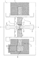
図1に、本発明の実施の形態の前提となるアクチュエータの構成を示す上面図を示す。具体的には、基板11の上には圧電体層の下部電極層となるグランド12が形成されており、グランド12には接続のための電極12fが形成されている。なお、同じハッチングは同じ層を示している。さらにグランド12の上には、圧電体層の上部電極層18が形成されている。なお、上部電極層18には、接続のための電極18fが設けられている。駆動アーム14は、第1のカンチレバー14aと、第2のカンチレバー14bと、接点14cと、ヒンジ部14d及び14eとを有する。
FIG. 1 is a top view showing a configuration of an actuator which is a premise of the embodiment of the present invention. Specifically, a
信号線13aは、一端が基板1に支持され、駆動アーム14と穴15との一部を覆うように延伸している。同様に、信号線13bは、一端が基板1に支持され、駆動アーム14と穴15との一部を覆うように延伸している。信号線13aと信号線13bとは、接点14c上で切断されており、上下対称となっている。そして、信号線13a及び13bの左右には、それらと平行に、駆動アーム14と穴15とを架橋するようにグランド線17a及び17bが形成されている。なお、図2は、信号線13a及び13bを取り除き、上面図における点線枠20内を拡大したものである。
One end of the
図3(a)に、上面図(図1)のA−A’線での概略断面図を示す。駆動アーム14の接点14cは、基板11の一部の層11cと、グランド層12cと、PZT(Pb(ZrTi)O3)等の圧電体層16cと、上部電極層18cとで構成される。なお、図3(a)の断面図では示されていないが、第1のカンチレバー14aは、基板11の一部の層11aと、グランド層12aと、PZT(Pb(ZrTi)O3)等の圧電体層16aと、上部電極層18aとで構成される。同様に、第2のカンチレバー14bは、基板11の一部の層11bと、グランド層12bと、PZT(Pb(ZrTi)O3)等の圧電体層16bと、上部電極層18bとで構成される。信号線13aは、一端が基板11に支持され、接点14cの一部と穴15とを覆うように延伸している。同様に、信号線13bも、一端が基板11に支持され、接点14cの一部と穴15とを覆うように延伸している。
FIG. 3A is a schematic cross-sectional view taken along line AA ′ of the top view (FIG. 1). The
そして、第1及び第2のカンチレバー14a及び14bに電圧を印加することにより、駆動アーム14を駆動させ、接点14cと信号線13a及び13bとを接触させる。具体的には、グランド層12a及び12bに負電圧を印加し、上部電極層18a及び18bに正電圧を印加することにより、駆動アームを引き上げる。アクチュエータをスイッチトとすると、接点14cと信号線13a及び13bとが接触することで導通する。なお、ヒンジ部14d及び14eによって、適切な形で接点14cが信号線13a及び13bに接触するようになる。
Then, by applying a voltage to the first and
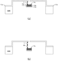
しかし、第1のカンチレバー14a及び第2のカンチレバー14bには反りが生じるため、駆動アーム14全体が反ることになる。例えば長さ500μmのカンチレバーでは、数十〜百μm程度の反りが生じる。すなわち、接点14cの位置は、実際には、図3(b)に示すように、図3(a)で示した位置よりも下がった位置になる。なお、図3(b)における長さMは、反りの量を示す。
However, since the
例えば図1乃至図3(b)に示したようなアクチュエータを用いた電気式微小機械スイッチ(以下、MEMSスイッチと呼ぶ場合もある)では、一般的に信号線13a及び13bと接点14cとの距離(長さL)を10μm以下に制御しなければならないが、第1のカンチレバー14a及び第2のカンチレバー14bに反りが生じるため、信号線13a及び13bと接点14cとの距離を一定に保つことができず、スイッチング電圧にばらつきが生じる。
For example, in an electric micromechanical switch using an actuator as shown in FIG. 1 to FIG. 3B (hereinafter sometimes referred to as a MEMS switch), the distance between the
そこで、本発明の実施の形態では、図4及び図5に示すような構成を採用する。以下、本発明の実施の形態について説明する。 Therefore, in the embodiment of the present invention, a configuration as shown in FIGS. 4 and 5 is adopted. Embodiments of the present invention will be described below.
図4に、本発明の実施の形態におけるアクチュエータを用いた電気式微小機械スイッチの上面図を示す。例えば、Siの基板1の表面には、SiO2の絶縁層が形成され、その上には、下部電極層となるグランド2が形成されている。また、基板1及びグランド2の上には上部電極層8が形成されている。なお、同じハッチングは同じ層を示している。駆動アーム4は、信号線3c及び3dと接する接触部4cと、接触部4cとヒンジ部4dを介して接続される第1のカンチレバー4aと、接触部4cとヒンジ部4eを介して接続される第2のカンチレバー4bとを有しており、穴5を架橋するように設けられている。なお、層の構成としては、駆動アーム4は、基板1の一部の層(図4ではグランド2によって隠れている)と、グランド2の層と、PZT等の圧電体層6(図4では上部電極層8によって隠れている)と、上部電極層8とを有する。また、ヒンジ部4d及び4eにおいては、ヒンジの機能を有効に果たすために穴が形成されている。
FIG. 4 shows a top view of an electric micromechanical switch using the actuator according to the embodiment of the present invention. For example, a SiO 2 insulating layer is formed on the surface of a Si substrate 1, and a ground 2 serving as a lower electrode layer is formed thereon. An upper electrode layer 8 is formed on the substrate 1 and the ground 2. The same hatching indicates the same layer. The drive arm 4 is connected via a contact part 4c contacting the
第1の固定アーム3aは、一端が基板1に支持され、駆動アーム4の接触部4cの一部と穴5の一部とを覆うように延伸している。そして、第1の固定アーム3aの先端(支持部と反対側)の部分は、幅が除々に狭くなるように形成されている。同様に、第2の固定アーム3bは、一端が基板1に支持され、駆動アーム4の接触部4cの一部と穴5の一部とを覆うように延伸している。そして、第2の固定アーム3bの先端(支持部と反対側)の部分は、幅が除々に狭くなるように形成されている。信号線3cと信号線3dとは、駆動アーム4の接触部4c上において切断されており、第1の固定アーム3aと第2の固定アーム3bとは上下対称になっている。なお、詳細は後で説明するが、第1の固定アーム3a及び第2の固定アーム3bにおいては、信号線3c及び3dの下部の一部に駆動アーム4と同じ層を有する。また、第1の固定アーム3a及び第2の固定アーム3bの左右には、それらと平行に、駆動アーム4と穴5とを架橋するようにグランド線7a及び7bが形成されている。
One end of the first
図5(a)に、上面図(図4)のC−C’線での概略断面図を示す。図5(a)では、駆動アーム4は、基板1の一部の層1cと、グランド層2cと、PZT(Pb(ZrTi)O3)等の圧電体層6cと、上部電極層8cとで構成される。なお、駆動アーム4の構成は、基本的には、前提となるアクチュエータの構成と同じである。また、図5(a)の断面図では示されていないが、第1のカンチレバー4aは、基板1の一部の層1aと、グランド層2aと、PZT(Pb(ZrTi)O3)等の圧電体層6aと、上部電極層8aとで構成される。同様に、第2のカンチレバー4bは、基板1の一部の層1bと、グランド層2bと、PZT(Pb(ZrTi)O3)等の圧電体層6bと、上部電極層8bとで構成される。
FIG. 5A is a schematic cross-sectional view taken along the line CC ′ of the top view (FIG. 4). In FIG. 5A, the drive arm 4 includes a part of the layer 1c of the substrate 1, a ground layer 2c, a piezoelectric layer 6c such as PZT (Pb (ZrTi) O 3 ), and an upper electrode layer 8c. Composed. The configuration of the drive arm 4 is basically the same as the configuration of the actuator that is the premise. Although not shown in the cross-sectional view of FIG. 5A, the first cantilever 4a includes a part of the layer 1a of the substrate 1, the ground layer 2a, PZT (Pb (ZrTi) O 3 ), and the like. The piezoelectric layer 6a and the upper electrode layer 8a are included. Similarly, the
第1の固定アーム3aは、基板1の一部の層1dと、グランド層2dと、圧電体層6dと、上部電極層8dと、信号線3cとで構成される。そして、一端が基板1に支持され、第1の固定アーム3aの先端の部分は、信号線3cのみが突起するように形成されている。同様に、第2の固定アーム3bは、基板1の一部の層1eと、グランド層2eと、圧電体層6eと、上部電極層8eと、信号線3dとで構成される。そして、一端が基板1に支持され、第2の固定アーム3bの先端の部分は、信号線3dのみが突起するように形成されている。
The first
本実施の形態においても、上で述べたように駆動アーム4には反りが生じるため、実際の駆動アーム4の位置は、図5(b)に示す位置になる。一方で、本実施の形態では、第1の固定アーム3a及び第2の固定アーム3bが、駆動アーム4と同じ層を有する構造となっているため、図5(b)に示すように、第1の固定アーム3a及び第2の固定アーム3bにも駆動アーム4と同程度の反りが生じることになる。すなわち、駆動アーム4と第1の固定アーム3a及び第2の固定アーム3bの先端部分との距離は変わらないため、材料の応力による影響を抑えられる。なお、反りの量は、片側支持構造を両端支持構造に変更したり、穴5の大きさを変更したりすることにより、調整可能である。
Also in this embodiment, since the drive arm 4 is warped as described above, the actual position of the drive arm 4 is the position shown in FIG. On the other hand, in the present embodiment, since the first
また、図4に示したMEMSスイッチは、駆動アーム4を駆動させることにより、駆動アーム4の接触部4cと信号線3c及び3dとが接触するようになっている。なお、駆動アーム4は、基本的には、前提となるアクチュエータと同じものであり、駆動アーム4を駆動させる仕組みについても、上で説明した仕組みと同じである。すなわち、上で説明したように、第1及び第2のカンチレバー4a及び4bに電圧を印加することにより、駆動アーム4を駆動させ、信号線3c及び3dと接触部4cとを接触させる。
Further, in the MEMS switch shown in FIG. 4, by driving the drive arm 4, the contact portion 4 c of the drive arm 4 and the
次に、図6乃至図9を用いて、図4及び図5に示したようなアクチュエータの製造方法を説明する。なお、図6乃至図9において、左側に示す断面図Bは図4のB−B’線での断面図を示し、右側に示す断面図Cは図4のC−C’線での断面図を示す。 Next, a method of manufacturing the actuator as shown in FIGS. 4 and 5 will be described with reference to FIGS. 6 to 9, the cross-sectional view B shown on the left side is a cross-sectional view taken along the line BB 'in FIG. 4, and the cross-sectional view C shown on the right side is a cross-sectional view taken along the line CC' in FIG. Indicates.
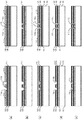
図6(a)に示すように、表面にSi層101、当該表面のSi層101より下にSiO2層102、そしてSiO2層102の下にSi層103が形成されているSOI(Silicon On Insulator)ウェハを用いる。そして、図6(b)に示すように、水又は酸素雰囲気中で、SOIウェハの上下面の表面を熱酸化させてSiO2層104及び105を形成する。このSiO2層104は、図4に示した、基板1の表面の絶縁層である。その後、図6(c)に示すように、スパッタによって圧電体層の下部電極層となるPt/Ti層106をSiO2層104の上に形成する。
As shown in FIG. 6 (a),
そして、図6(d)に示すように、SOIウェハを回転させ、PZTゾルゲルの成膜を1μm程度行って、PZT圧電体層107をPt/Ti層106の上に形成する。次に、図6(e)に示すように、再度スパッタによって圧電体層の上部電極となるPt/Ti層108をPZT圧電体層107の上に形成する。ここまでは、断面図B及び断面図C共に変わりない。
Then, as shown in FIG. 6D, the SOI wafer is rotated, and the PZT sol-gel film is formed by about 1 μm to form the PZT
次に、フォトレジストを塗布し、フォトマスクを透過させて露光し、感光したレジストを現像し、ポジ型のレジストの場合は感光した部分、ネガ型のレジストの場合は感光しなかった部分のレジストを除去して、図7(a)に示すように、Pt/Ti層108及びPZT圧電体層107をエッチングするためのレジスト層109を形成する。断面図Bでは、第1及び第2のカンチレバー4a及び4bと、接触部4cとを切断するため、2つの溝110a及び110bが形成される。一方、断面図Cでは、第1及び第2の固定アーム3a及び3bと、接触部4cとを切断するため、2つの溝112a及び112bが形成される。
Next, a photoresist is applied, exposed through a photomask, exposed, and the exposed resist is developed. In the case of a positive type resist, the exposed portion, in the case of a negative type resist, the portion of the resist that has not been exposed. As shown in FIG. 7A, a resist
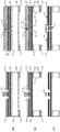
そして、図7(b)に示すように、エッチングでレジスト層109が形成されていない部分のPt/Ti層108及びPZT圧電体層107が削られ、その後レジスト層109が除去される。次に、下部電極層であるPt/Ti層106と、SiO2層104と、Si層101と、SiO2層102とを加工するために、フォトレジストを塗布し、フォトマスクを透過させて露光し、感光したレジストを現像し、感光した部分又は感光しなかった部分のレジストを除去して、図7(c)に示すように、レジスト層111を形成する。なお、断面図Bでは、上部全面にレジスト層111が形成されるが、断面図Cでは、第1及び第2の固定アーム3a及び3bと、接触部4cとを切断するために、2つの溝112a及び112bが形成される。
Then, as shown in FIG. 7B, the Pt /
その後、図7(d)に示すように、エッチングで、レジスト層111が形成されていない部分のPt/Ti層106と、SiO2層104と、Si層101と、SiO2層102とが削られ、その後レジスト層111が除去される。なお、ヒンジ部4d及び4eについてはここでは説明を省略している。このヒンジ部4d及び4eを形成するためには、図7(c)の段階で断面図Bにもレジストが形成されない部分が適切に形成される必要がある。
Thereafter, as shown in FIG. 7D, the Pt /
次に、Auの信号線3c及び3dを形成する前段階として、図7(e)に示すように、溝110a及び110bと、溝112a及び112bとに埋め込み用レジスト113を塗布する。そして、信号線3c及び3dを形成するために、フォトレジストを塗布し、フォトマスクを透過させて露光し、感光したレジストを現像し、感光した部分又は感光しなかった部分のレジストを除去して、図8(a)に示すように、犠牲層114を形成する。犠牲層114は、図5(a)に示した長さLを実現するための厚みを有する。その後、図8(b)に示すように、犠牲層114の上に、スパッタで、Au層115を形成する。
Next, as a step before forming the
そして、フォトレジストを塗布し、フォトマスクを透過させて露光し、感光したレジストを現像し、感光した部分又は感光しなかった部分のレジストを除去して、図8(c)に示すように、レジスト層116を形成する。断面図Bでは、Au層115のうちAu層115aのみが信号線として用いられるため、Au層115aの上部にのみレジスト層116を形成する。一方、断面図Cでは、信号線3cと信号線3dとに分離するために、溝117が形成される。その後、図8(d)に示すように、エッチングで、レジスト層116が形成されていない部分のAu層115を削り取る。
Then, applying a photoresist, exposing through a photomask, developing the exposed resist, removing the exposed or unexposed resist, as shown in FIG. A resist
次に、裏面のSiO2層105の下に、フォトレジストを塗布し、フォトマスクを透過させて露光し、感光したレジストを現像し、感光した部分又は感光しなかった部分のレジストを除去して、図9(a)に示すように、レジスト層118を形成する。そして、下部からエッチングを行って、図9(b)に示すように、レジスト層118が形成されていない部分における、SiO2層105、Si層103と、SiO2層102とを削り取る。
Next, a photoresist is applied under the SiO 2 layer 105 on the back surface, exposed through a photomask, exposed to photosensitive resist, and exposed or unexposed portions of resist are removed. As shown in FIG. 9A, a resist
その後、埋め込み用レジスト113と、犠牲層114と、レジスト層116と、レジスト層118とを除去し、超臨界乾燥を実施すると、図9(c)に示すように、完成する。断面図Cでは、第1の固定アーム3a及び第2の固定アーム3bは、信号線3c及び3dの下部に駆動アーム4と同じ層を有し、先端部分は、信号線3c及び3dのみがそれぞれ突起するようになっている。すなわち、駆動アーム4と、第1の固定アーム3a及び第2の固定アーム3bとに同程度の反りが生じ、駆動アーム4と第1の固定アーム3a及び第2の固定アーム3bの先端部分との距離は変わらないため、材料の応力による影響を抑えられる。また、信号線3c及び3dの下部に駆動アーム4と同じ層を有するので、信号線3c及び3dを補強できている。
Thereafter, the embedding resist 113, the
以上述べたような製造プロセスを実施することによって、図4及び図5で示したようなアクチュエータを製造することができる。なお、レジスト層を形成する部分が異なるが、基本的には、前提となるアクチュエータの製造プロセスをそのまま応用して製造することができる。また、上で述べた各層は、特に触れなかった場合にはnmレベルの厚さとなる。 By performing the manufacturing process as described above, the actuator as shown in FIGS. 4 and 5 can be manufactured. In addition, although the part which forms a resist layer differs, fundamentally, it can manufacture by applying the manufacturing process of a presupposed actuator as it is. In addition, each layer described above has a thickness of nm level unless otherwise touched.
以上本発明の一実施の形態について説明したが、本発明はこれに限定されるものではない。例えば細かい構造は、全て同じでなければならないわけではない。ヒンジ部の構造は、他のヒンジ構造を採用することも可能である。 Although one embodiment of the present invention has been described above, the present invention is not limited to this. For example, the fine structure does not have to be all the same. Other hinge structures can be adopted as the structure of the hinge portion.
また、上では、固定アームと駆動アームとがねじれの関係になるようなMEMSスイッチを例に説明したが、図10に示すような構造に変形することも可能である。なお、図10は上面図である。図10では、駆動アーム24bは、一端が基板21に支持され、穴25を覆うように延伸している。そして、固定アーム24aは、一端が基板21に支持され、固定アーム24aの先端(信号線23a)が駆動アーム24bの先端を覆うように形成されている。すなわち、固定アーム24aと駆動アーム24bとが直列に形成されている。より具体的には、基板21の表面には、SiO2の絶縁層が形成され、その上には、下部電極層となるグランド22a及び22bが形成されている。グランド22aの上には圧電体層(図10では上部電極層28aによって隠れている)と上部電極層28aとが形成されており、さらに上部電極層28aの上には信号線23aが形成されている。また、グランド22bの上には圧電体層(図10では上部電極層28bによって隠れている)と上部電極層28bとが形成されており、さらに上部電極層28bの上には信号線23bが形成されている。
In the above description, the MEMS switch in which the fixed arm and the drive arm are in a twisted relationship has been described as an example. However, the MEMS switch may be modified into a structure as shown in FIG. FIG. 10 is a top view. In FIG. 10, one end of the
図11に、図10のD−D’線での断面図を示す。図11では、固定アーム24aは、一端が基板21に支持され、基板21の一部の層と、グランド22aと、圧電体層26aと、上部電極層28aと信号線23aとを有する。そして、固定アーム24aの先端の部分は、信号線23aのみが突起するように形成されている。また、駆動アーム24bは、一端が基板21に支持され、基板21の一部の層と、グランド22bと、圧電体層26bと、上部電極層28bと信号線23bとを有する。そして、駆動アーム24bに電圧を印加することにより、駆動アーム24bを引き上げ、信号線23bを信号線23aに接触させる。この場合においても、固定アーム24a及び駆動アーム24bには同程度の反りが生じることになるので、信号線23aと信号線23bとの距離は変わらず、材料の応力による影響を抑えられる。このように、固定アームと駆動アームとの位置関係は、固定アームの信号線の先端が駆動アームと重なるようになっていればよい。
FIG. 11 is a cross-sectional view taken along line D-D ′ in FIG. 10. In FIG. 11, one end of the fixed
1 基板 2 グランド
3a 第1の固定アーム
3b 第2の固定アーム
3c,3d 信号線
4 駆動アーム
4a 第1のカンチレバー
4b 第2のカンチレバー
4c 接触部
4d,4e ヒンジ部
5 穴
7a,7b グランド線
8 上部電極層
DESCRIPTION OF SYMBOLS 1 Board | substrate 2
Claims (4)
圧電体層と当該圧電体層の上下に電極層とを有する圧電駆動部が一方の面に形成され且つ少なくとも一端が前記基板に固定された駆動アームと、
信号線と当該信号線の下部の一部に前記駆動アームと同じ層とを有し且つ少なくとも一端が前記基板に固定された固定アームと、
を有し、
前記駆動アーム及び前記固定アームが、前記基板の開口部の一部を覆っており、
前記固定アームにおける前記信号線が、前記駆動アーム上に延伸しており、前記駆動アームと重なる部分において前記駆動アームと接することができるようになっている
電気式微小機械スイッチ。 A substrate having an opening;
A driving arm having a piezoelectric layer having a piezoelectric layer and electrode layers above and below the piezoelectric layer formed on one surface and at least one end fixed to the substrate;
A fixed arm having a signal line and the same layer as the drive arm at a part of the lower part of the signal line and at least one end fixed to the substrate
Have
The drive arm and the fixed arm cover a part of the opening of the substrate;
The electric micromechanical switch, wherein the signal line in the fixed arm extends on the drive arm and can come into contact with the drive arm at a portion overlapping the drive arm.
請求項1記載の電気式微小機械スイッチ。 The electric micromechanical switch according to claim 1, wherein the driving arm is driven to contact the signal line according to the piezoelectric layer by a voltage applied to the electrode layer.
請求項1記載の電気式微小機械スイッチ。 The electric micromechanical switch according to claim 1, wherein the fixed arm has the same layer as the drive arm in a portion other than a portion overlapping the drive arm.
ことを特徴とする請求項1記載の電気式微小機械スイッチ。 The electric micromechanical switch according to claim 1, wherein the fixed arm extends on the drive arm so as to be in a twisted relationship with the drive arm or in a series relationship with the drive arm. .
Priority Applications (1)
| Application Number | Priority Date | Filing Date | Title |
|---|---|---|---|
| JP2008114803A JP5118546B2 (en) | 2008-04-25 | 2008-04-25 | Electric micro mechanical switch |
Applications Claiming Priority (1)
| Application Number | Priority Date | Filing Date | Title |
|---|---|---|---|
| JP2008114803A JP5118546B2 (en) | 2008-04-25 | 2008-04-25 | Electric micro mechanical switch |
Publications (2)
| Publication Number | Publication Date |
|---|---|
| JP2009266615A JP2009266615A (en) | 2009-11-12 |
| JP5118546B2 true JP5118546B2 (en) | 2013-01-16 |
Family
ID=41392189
Family Applications (1)
| Application Number | Title | Priority Date | Filing Date |
|---|---|---|---|
| JP2008114803A Expired - Fee Related JP5118546B2 (en) | 2008-04-25 | 2008-04-25 | Electric micro mechanical switch |
Country Status (1)
| Country | Link |
|---|---|
| JP (1) | JP5118546B2 (en) |
Cited By (1)
| Publication number | Priority date | Publication date | Assignee | Title |
|---|---|---|---|---|
| RU2705792C1 (en) * | 2018-12-26 | 2019-11-12 | федеральное государственное автономное образовательное учреждение высшего образования "Южный федеральный университет" (Южный федеральный университет) | Integrated microelectromechanical switch |
Families Citing this family (3)
| Publication number | Priority date | Publication date | Assignee | Title |
|---|---|---|---|---|
| JP5323988B2 (en) * | 2010-09-27 | 2013-10-23 | 太陽誘電株式会社 | MEMS switch |
| JP2013114755A (en) * | 2011-11-25 | 2013-06-10 | Taiyo Yuden Co Ltd | Switch device and method of manufacturing the same |
| JP2013118234A (en) * | 2011-12-02 | 2013-06-13 | Taiyo Yuden Co Ltd | Piezoelectric actuator and method of manufacturing the same |
Family Cites Families (3)
| Publication number | Priority date | Publication date | Assignee | Title |
|---|---|---|---|---|
| DE19736674C1 (en) * | 1997-08-22 | 1998-11-26 | Siemens Ag | Micromechanical electrostatic relay |
| ATE392010T1 (en) * | 1999-02-04 | 2008-04-15 | Inst Of Microelectronics | MICRO RELAY |
| JP4417861B2 (en) * | 2005-01-31 | 2010-02-17 | 富士通株式会社 | Micro switching element |
-
2008
- 2008-04-25 JP JP2008114803A patent/JP5118546B2/en not_active Expired - Fee Related
Cited By (1)
| Publication number | Priority date | Publication date | Assignee | Title |
|---|---|---|---|---|
| RU2705792C1 (en) * | 2018-12-26 | 2019-11-12 | федеральное государственное автономное образовательное учреждение высшего образования "Южный федеральный университет" (Южный федеральный университет) | Integrated microelectromechanical switch |
Also Published As
| Publication number | Publication date |
|---|---|
| JP2009266615A (en) | 2009-11-12 |
Similar Documents
| Publication | Publication Date | Title |
|---|---|---|
| KR100702019B1 (en) | Micro mirror device | |
| JP4102037B2 (en) | Micromirror device and manufacturing method thereof | |
| JP5140041B2 (en) | System and method for thermal isolation of silicon structures | |
| JP4328980B2 (en) | Piezoelectric vibrator and manufacturing method thereof, MEMS device and manufacturing method thereof | |
| JP2005279919A (en) | Micro movable device and manufacturing method of the same | |
| JP5118546B2 (en) | Electric micro mechanical switch | |
| KR100790878B1 (en) | Etching Method for decoupled comb electrodes by self-alignment | |
| JP4739173B2 (en) | Micro switching element | |
| JP3910333B2 (en) | Galvano micromirror and manufacturing method thereof | |
| JP5320625B2 (en) | Actuator and manufacturing method thereof | |
| JP2008194813A (en) | Moving element and method of manufacturing the same | |
| JP2008167508A (en) | Actuator and manufacturing method of actuator | |
| JP5314932B2 (en) | Electric micro mechanical switch | |
| JP2007183662A (en) | Micromirror element and method of manufacturing same | |
| JP2007030090A (en) | Method for forming microstructure | |
| JP5180683B2 (en) | Switched capacitor | |
| TWI384518B (en) | Low pull-in voltage rf-mems switch and method for preparing the same | |
| JP2006221956A (en) | Fuse | |
| JP5679058B2 (en) | Electronic device, manufacturing method thereof, and driving method of electronic device | |
| JP2008213057A (en) | Vibrator structure and its manufacturing method | |
| JP3869438B2 (en) | MEMS device, manufacturing method thereof, and optical device | |
| JP2004306208A (en) | Micro-electromechanical system element and manufacturing method thereof | |
| JP3825388B2 (en) | Optical switch device | |
| JP5277977B2 (en) | Optical device | |
| JP2008141567A (en) | Piezoelectric vibrator and manufacturing method therefor |
Legal Events
| Date | Code | Title | Description |
|---|---|---|---|
| A621 | Written request for application examination |
Free format text: JAPANESE INTERMEDIATE CODE: A621 Effective date: 20110328 |
|
| A977 | Report on retrieval |
Free format text: JAPANESE INTERMEDIATE CODE: A971007 Effective date: 20120910 |
|
| TRDD | Decision of grant or rejection written | ||
| A01 | Written decision to grant a patent or to grant a registration (utility model) |
Free format text: JAPANESE INTERMEDIATE CODE: A01 Effective date: 20120925 |
|
| A01 | Written decision to grant a patent or to grant a registration (utility model) |
Free format text: JAPANESE INTERMEDIATE CODE: A01 |
|
| A61 | First payment of annual fees (during grant procedure) |
Free format text: JAPANESE INTERMEDIATE CODE: A61 Effective date: 20121019 |
|
| R150 | Certificate of patent or registration of utility model |
Free format text: JAPANESE INTERMEDIATE CODE: R150 Ref document number: 5118546 Country of ref document: JP Free format text: JAPANESE INTERMEDIATE CODE: R150 |
|
| FPAY | Renewal fee payment (event date is renewal date of database) |
Free format text: PAYMENT UNTIL: 20151026 Year of fee payment: 3 |
|
| R250 | Receipt of annual fees |
Free format text: JAPANESE INTERMEDIATE CODE: R250 |
|
| R250 | Receipt of annual fees |
Free format text: JAPANESE INTERMEDIATE CODE: R250 |
|
| R250 | Receipt of annual fees |
Free format text: JAPANESE INTERMEDIATE CODE: R250 |
|
| R250 | Receipt of annual fees |
Free format text: JAPANESE INTERMEDIATE CODE: R250 |
|
| LAPS | Cancellation because of no payment of annual fees |