JP5115518B2 - Electronic equipment - Google Patents

Electronic equipment Download PDF

Info

Publication number
JP5115518B2
JP5115518B2 JP2009120267A JP2009120267A JP5115518B2 JP 5115518 B2 JP5115518 B2 JP 5115518B2 JP 2009120267 A JP2009120267 A JP 2009120267A JP 2009120267 A JP2009120267 A JP 2009120267A JP 5115518 B2 JP5115518 B2 JP 5115518B2
Authority
JP
Japan
Prior art keywords
woven fabric
circuit board
conductive
electronic device
packing tool
Prior art date
Legal status (The legal status is an assumption and is not a legal conclusion. Google has not performed a legal analysis and makes no representation as to the accuracy of the status listed.)
Expired - Fee Related
Application number
JP2009120267A
Other languages
Japanese (ja)
Other versions
JP2010267928A (en
Inventor
和雅 黒川
Current Assignee (The listed assignees may be inaccurate. Google has not performed a legal analysis and makes no representation or warranty as to the accuracy of the list.)
Denso Corp
Original Assignee
Denso Corp
Priority date (The priority date is an assumption and is not a legal conclusion. Google has not performed a legal analysis and makes no representation as to the accuracy of the date listed.)
Filing date
Publication date
Application filed by Denso Corp filed Critical Denso Corp
Priority to JP2009120267A priority Critical patent/JP5115518B2/en
Publication of JP2010267928A publication Critical patent/JP2010267928A/en
Application granted granted Critical
Publication of JP5115518B2 publication Critical patent/JP5115518B2/en
Expired - Fee Related legal-status Critical Current
Anticipated expiration legal-status Critical

Links

Images

Description

本発明は、回路基板の電磁波シールドを行う基板梱包具に回路基板が収容された電子装置に関する。   The present invention relates to an electronic device in which a circuit board is accommodated in a board packing tool that performs electromagnetic wave shielding of the circuit board.

各種の電子機器においては、EMI(ElectroMagnetic Interference)への対策のため、すなわち内部からの電磁波の漏洩および外部からの電磁波の侵入を防ぐため、種々の電磁波シールド手段が講じられている。   In various electronic devices, various electromagnetic wave shielding means are taken for measures against EMI (ElectroMagnetic Interference), that is, in order to prevent leakage of electromagnetic waves from the inside and intrusion of electromagnetic waves from the outside.

電磁波シールド手段としては、金属筐体を用いる方法や、樹脂筐体の内面に無電解メッキ等で導電性層を設ける方法が一般的である。また、例えば特許文献1に示されるように、筐体内部に収容される回路基板を、導電性の袋で覆う方法も提案されている。   As the electromagnetic wave shielding means, a method using a metal casing or a method of providing a conductive layer on the inner surface of a resin casing by electroless plating or the like is general. For example, as shown in Patent Document 1, a method of covering a circuit board accommodated in a housing with a conductive bag has also been proposed.

特許文献1に示される方法では、導電性織布などからなる導電体層の一面上に絶縁体層、裏面上にヒートシール性絶縁体層を配置してなる多層シートを、ヒートシール性絶縁体層が内側となるように二つ折りにし、両サイドを、ヒートシールするとともに導電糸でミシン縫いしている。また、コネクタケーブルが引き出される残りの開口部では導電体層が露出しており、回路基板を収容した状態で、これらを導電性接着テープで固定することで、袋状としている。このようにして、多層シートからシールド用の袋を形成し、回路基板に対して全方位の電磁波シールドを達成している。   In the method disclosed in Patent Document 1, a multilayer sheet in which an insulating layer is disposed on one surface of a conductive layer made of a conductive woven fabric or the like and a heat-sealable insulating layer is disposed on the back surface is used as a heat-sealable insulator. It is folded in half so that the layer is on the inside, and both sides are heat sealed and sewn with conductive thread. Further, the conductor layer is exposed in the remaining opening from which the connector cable is pulled out, and in a state where the circuit board is accommodated, these are fixed with a conductive adhesive tape to form a bag. In this way, a shielding bag is formed from the multilayer sheet, and electromagnetic wave shielding in all directions with respect to the circuit board is achieved.

ところで、上記した金属筐体、内面メッキされた樹脂筐体、導電体層を備えたシールド用の袋は、GND電位に固定、すなわち接地されることで、電磁波シールドとして機能する。例えば特許文献2(図6参照)に示されるように、金属材料からなる接点ばねにより、上記した金属筐体などと回路基板のGNDパターンとの電気的接続状態を良好に確保しつつ、金属筐体などをGND電位に固定する構成が知られている。   By the way, the shielding bag provided with the metal casing, the resin casing plated on the inner surface, and the conductor layer functions as an electromagnetic wave shield by being fixed to the GND potential, that is, grounded. For example, as shown in Patent Document 2 (see FIG. 6), the contact spring made of a metal material ensures a good electrical connection between the above-described metal housing and the GND pattern of the circuit board, while ensuring good electrical connection. A configuration for fixing a body or the like to the GND potential is known.

特開平7−245496号公報JP-A-7-245496 特開2007−314026号公報JP 2007-314026 A

金属筐体を用いる方法は、筐体自体が重くなってしまい、軽量化の要求に反してしまう。また、樹脂筐体の内面に無電解メッキ等で導電性層を設ける方法は、金属筐体に比べて軽量化することができる反面、メッキ等による導電性層が製造中の擦れ等によって剥がれ易く、導電性層が剥がれると電磁波シールド効果がなくなるという問題がある。   In the method using a metal casing, the casing itself becomes heavy, which is against the demand for weight reduction. In addition, the method of providing a conductive layer on the inner surface of a resin casing by electroless plating can reduce the weight compared to a metal casing, but the conductive layer by plating or the like is easily peeled off due to rubbing during manufacture. When the conductive layer is peeled off, there is a problem that the electromagnetic wave shielding effect is lost.

一方、特許文献1に示される方法では、シールド用の袋が、導電性織布などの導電体層を含む多層シートからなるので、金属筐体に比べて軽量化することができる。また、ヒートシール性絶縁体層が袋の内面をなしているので、製造途中に擦れ等があっても、電磁波シールド効果を確保することができるとともに、回路基板に構成された回路のうちのGND電位に固定される部位を除く部位と、シールド用の袋とのショートを防ぐことができる。   On the other hand, in the method disclosed in Patent Document 1, since the shielding bag is made of a multilayer sheet including a conductive layer such as a conductive woven fabric, the weight can be reduced as compared with a metal casing. In addition, since the heat-sealable insulating layer forms the inner surface of the bag, the electromagnetic wave shielding effect can be ensured even if there is rubbing or the like during the manufacturing, and the GND of the circuit configured on the circuit board can be secured. Short-circuiting between the part excluding the part fixed to the potential and the shielding bag can be prevented.

しかしながら、特許文献1に示される方法では、ヒートシール性絶縁体層が袋の内面をなすため、特許文献2に示される接点ばねを、導電体層(導電性織布)に直接的に接触させることができない。例えば接点ばね以外の手段により、導電体層(導電性織布)をGND電位に固定させることも考えられるが、接点ばねのように弾性変形を利用して電気的接続状態を良好に確保することができないため、シールド性が低下する恐れがある。   However, in the method shown in Patent Document 1, since the heat-sealable insulating layer forms the inner surface of the bag, the contact spring shown in Patent Document 2 is brought into direct contact with the conductor layer (conductive cloth). I can't. For example, it is conceivable to fix the conductor layer (conductive woven fabric) to the GND potential by means other than the contact spring. However, as in the case of the contact spring, the electrical connection state should be ensured satisfactorily using elastic deformation. Shielding performance may be deteriorated.

本発明は上記問題点に鑑み、軽量で、回路基板とのショートを防ぎつつ電磁波シールド効果を確保することのできる電子装置を提供することを目的とする。   In view of the above problems, an object of the present invention is to provide an electronic device that is lightweight and can ensure an electromagnetic wave shielding effect while preventing a short circuit with a circuit board.

上記目的を達成する為に請求項1に記載の電子装置は、第1主面及び該第1主面の裏面である第2主面の少なくとも一方に電子部品が実装された回路基板と、回路基板を内部空間に収容し、回路基板の電磁波シールドを行う基板梱包具と、金属材料からなり、回路基板における第1主面に実装されて、回路基板のGNDパターンと基板梱包具とを電気的に接続する接点ばねと、を備えており、基板梱包具が、樹脂織布を金属メッキした導電性織布と樹脂織布からなる非導電性織布との積層織布を、少なくとも回路基板の第1主面側を覆う部位として含むとともに、非導電性織布が基板梱包具の内面をなしている。そして、積層織布に導電性の中継部材が固定され、この中継部材が、導電性織布と電気的に接続されるとともに、基板梱包具の内面をなす非導電性織布の表面において接点ばねの接触部位に配置されていることを特徴とする。   In order to achieve the above object, an electronic device according to claim 1 includes a circuit board having an electronic component mounted on at least one of a first main surface and a second main surface which is the back surface of the first main surface, and a circuit. A board packing tool that accommodates the board in the internal space and shields the electromagnetic wave of the circuit board, and is made of a metal material and mounted on the first main surface of the circuit board to electrically connect the GND pattern of the circuit board and the board packing tool. And a contact spring connected to the circuit board, wherein the substrate packing device comprises at least a laminated woven fabric of a conductive woven fabric obtained by metal-plating a resin woven fabric and a non-conductive woven fabric made of a resin woven fabric. While including as a site | part which covers the 1st main surface side, the nonelectroconductive woven fabric has comprised the inner surface of the board | substrate packing tool. A conductive relay member is fixed to the laminated woven fabric. The relay member is electrically connected to the conductive woven fabric, and a contact spring is formed on the surface of the non-conductive woven fabric forming the inner surface of the substrate packing device. It is arrange | positioned in the contact part of.

本発明では、基板梱包具が、樹脂織布を金属メッキした導電性織布と樹脂織布からなる非導電性織布との積層織布を、少なくとも回路基板の第1主面側を覆う部位として含んでいる。積層織布の主材料は樹脂織布であるので、従来の金属筐体に比べて、電子装置を軽量化することができる。   In the present invention, the substrate packing tool covers at least the first main surface side of the circuit board with a laminated woven fabric of a conductive woven fabric obtained by metal plating a resin woven fabric and a non-conductive woven fabric made of the resin woven fabric. Includes as. Since the main material of the laminated woven fabric is a resin woven fabric, the electronic device can be reduced in weight compared to a conventional metal casing.

また、積層織布において、非導電性織布が基板梱包具の内面をなしているので、積層織布を特に成形体としなくとも、回路基板に構成された回路のうちのGND電位に固定される部位を除く部位と、基板梱包具とのショートを防ぐことができる。   Further, in the laminated woven fabric, since the non-conductive woven fabric forms the inner surface of the substrate packing tool, even if the laminated woven fabric is not particularly formed, it is fixed to the GND potential of the circuit configured on the circuit board. It is possible to prevent a short circuit between the part excluding the part to be attached and the substrate packing tool.

また、非導電性織布が基板梱包具の内面をなしているので、回路基板を基板梱包具の内部空間に収容する際に、回路基板に実装された電子部品が導電性織布に接触しがたく、金属メッキ層の剥がれを抑制することができる。なお、積層織布を構成している導電性織布は、樹脂織布を金属メッキしたもので、金属メッキされた樹脂繊維が立体的に絡み合った構造となっている。すなわち、該導電性織布の金属メッキ層は、従来の樹脂筐体に設けられた導電性層のような筐体表面にだけあるものではない。したがって、基板梱包具の外面をなす導電性織布に擦れ等があっても、導電性織布の金属メッキ層のうち、その厚さ方向の一部(例えば表面のみ)が剥がれる程度であり、電磁波シールド効果も損なわれ難い。   In addition, since the non-conductive woven cloth forms the inner surface of the board packing tool, when the circuit board is accommodated in the internal space of the board packing tool, the electronic components mounted on the circuit board come into contact with the conductive woven cloth. The peeling of the metal plating layer can be suppressed. The conductive woven fabric constituting the laminated woven fabric is obtained by metal-plating a resin woven fabric, and has a structure in which metal-plated resin fibers are entangled three-dimensionally. That is, the metal plating layer of the conductive woven fabric is not only on the surface of the case like the conductive layer provided on the conventional resin case. Therefore, even if there is rubbing or the like on the conductive woven fabric that forms the outer surface of the substrate packing tool, a part of the metal plating layer of the conductive woven fabric (for example, only the surface) is peeled off, The electromagnetic shielding effect is not easily lost.

また、導電性の中継部材が、導電性織布と電気的に接続されるとともに、非導電性織布の表面において接点ばねの接触部位に配置されているため、非導電性織布が基板梱包具の内面をなす構成でありながら、接点ばねの弾性変形により、回路基板のGNDパターンと基板梱包具(導電性織布)との電気的接続状態を良好に確保することができる。すなわち、基板梱包具を電磁波シールドとして効果的に機能させることができる。   In addition, since the conductive relay member is electrically connected to the conductive woven fabric and disposed at the contact portion of the contact spring on the surface of the nonconductive woven fabric, the nonconductive woven fabric is packaged on the board. Although it is the structure which makes the inner surface of a tool, the electrical connection state of the GND pattern of a circuit board and a board | substrate packing tool (conductive woven fabric) can be favorably ensured by the elastic deformation of a contact spring. That is, the substrate packing tool can be effectively functioned as an electromagnetic wave shield.

以上から、本発明の電子装置によれば、軽量で、回路基板とのショートを防ぎつつ電磁波シールド効果を確保することができる。   As described above, according to the electronic device of the present invention, it is lightweight and can secure an electromagnetic shielding effect while preventing a short circuit with the circuit board.

中継部材としては、請求項2に記載のように、導電性を有する導電糸を採用し、導電糸により、導電性織布と非導電性織布とが縫われた構成としても良い。また、請求項3に記載のように、中継部材が金属材料からなり、導電性織布と非導電性織布とに接触して積層織布にかしめ固定された構成としても良い。   As the relay member, as described in claim 2, a conductive yarn having conductivity may be adopted, and a conductive woven fabric and a non-conductive woven fabric may be sewn by the conductive yarn. According to a third aspect of the present invention, the relay member may be made of a metal material and contacted with the conductive woven fabric and the non-conductive woven fabric to be caulked and fixed to the laminated woven fabric.

特に前者(導電糸)によれば、中継部材を積層織布に固定するための貫通孔が不要であるので、製造工程を簡素化し、製造コストを低減することができる。また、積層織布に貫通孔を設けなくとも良いので、電磁波シールド効果を高めることもできる。   In particular, according to the former (conductive yarn), since a through hole for fixing the relay member to the laminated woven fabric is unnecessary, the manufacturing process can be simplified and the manufacturing cost can be reduced. Moreover, since it is not necessary to provide a through-hole in the laminated woven fabric, the electromagnetic wave shielding effect can be enhanced.

請求項4に記載のように、接点ばねは、回路基板に実装されたコネクタのシールドとして、コネクタの周辺に設けられた構成とすることが好ましい。このように、接点ばねがコネクタのシールドとして機能すると、外部からコネクタを介して回路基板に侵入する外来ノイズを、GNDとしての基板梱包具(導電性織布)へ効果的に逃がすことができる。また、基板梱包具にはコネクタ用の貫通孔が設けられているが、貫通孔の周辺に接点ばねが位置するので、貫通孔を介して出入する電磁波を効果的にシールドすることができる。   According to a fourth aspect of the present invention, the contact spring is preferably provided around the connector as a shield of the connector mounted on the circuit board. Thus, when the contact spring functions as a shield for the connector, external noise that enters the circuit board from the outside through the connector can be effectively released to the board packing tool (conductive woven cloth) as GND. Moreover, although the through hole for a connector is provided in the board packaging tool, since the contact spring is located around the through hole, it is possible to effectively shield electromagnetic waves entering and exiting through the through hole.

基板梱包具としては、例えば請求項5に記載のように、積層織布の成形体としての、回路基板の第1主面側を覆う第1成形体、及び、回路基板の第2主面側を覆う第2成形体からなる構成としても良い。これによれば、基板梱包具が2つの成形体からなるので、回路基板を収容すべく所定形状及び大きさの内部空間を確保し、回路基板と基板梱包具との接触を抑制することができる。   As a board | substrate packing tool, the 1st molded object which covers the 1st main surface side of a circuit board as a molded object of laminated woven fabric, for example as described in Claim 5, and the 2nd main surface side of a circuit board It is good also as a structure which consists of a 2nd molded object which covers. According to this, since the board packing tool is composed of two molded bodies, an internal space having a predetermined shape and size can be secured to accommodate the circuit board, and contact between the circuit board and the board packing tool can be suppressed. .

また、請求項6に記載のように、積層織布の成形体からなり、回路基板の第1主面側を覆う部位と、回路基板の第2主面側を覆う部位とが一体成形された構成としても良い。これによれば、請求項5に記載の発明と同じ効果を奏するとともに、成形体が所謂卵パック様となっているので、成形体から基板梱包具を形成する工程を簡素化することができる。   In addition, as described in claim 6, the part is formed of a laminated woven fabric, and a part covering the first main surface side of the circuit board and a part covering the second main surface side of the circuit board are integrally formed. It is good also as a structure. According to this, while having the same effect as the invention according to the fifth aspect, since the molded body has a so-called egg pack shape, the process of forming the substrate packing tool from the molded body can be simplified.

さらに、請求項7に記載のように、回路基板の第1主面側を覆う部位として、積層織布の成形体を有するともに、回路基板の第2主面側を覆う部位として、金属板を有する構成を採用することもできる。これによれば、請求項5同様、回路基板と基板梱包具との接触を抑制することができる。また、金属板を含む分、請求項5,6に記載の構成よりも重くなるものの、従来の金属筐体よりは、電子装置を軽量化することができる。   Furthermore, as described in claim 7, as a part covering the first main surface side of the circuit board, the metal plate is provided as a part covering the second main surface side of the circuit board while having a molded body of the laminated woven fabric. It is also possible to adopt a configuration having this. According to this, as in the fifth aspect, the contact between the circuit board and the board packing tool can be suppressed. Moreover, although it becomes heavier than the structure of Claims 5 and 6 by the part containing a metal plate, an electronic device can be reduced in weight rather than the conventional metal housing | casing.

請求項8に記載のように、成形体が、圧空成形により形成されてなる構成とすると良い。これによれば、成形体を、肉薄軽量で安価に製造することができる。しかしながら、圧空成形以外にも、真空成形や、熱プレスなどを採用することもできる。   As described in claim 8, it is preferable that the molded body is formed by pressure forming. According to this, a molded object can be manufactured thinly, lightweight and inexpensively. However, in addition to pressure forming, vacuum forming, hot pressing, or the like can be employed.

第1実施形態に係る電子装置の概略構成を示す平面図である。It is a top view which shows schematic structure of the electronic device which concerns on 1st Embodiment. 基板梱包具の概略構成を示す平面図である。It is a top view which shows schematic structure of a board | substrate packing tool. 図1のIII−III線に沿う断面図である。It is sectional drawing which follows the III-III line of FIG. 中継部材の概略構成を示す図であり、(a)は基板梱包具の外面側から見た平面図、b)は(a)のIVb−IVb線に沿う断面図である。It is a figure which shows schematic structure of a relay member, (a) is the top view seen from the outer surface side of the board | substrate packaging tool, b) is sectional drawing which follows the IVb-IVb line | wire of (a). 中継部材の変形例を示す平面図である。It is a top view which shows the modification of a relay member. 第2実施形態に係る電子装置のうち、中継部材の概略構成を示す図であり、(a)は平面図、(b)は(a)のVIb−VIb線に沿う断面図である。It is a figure which shows schematic structure of a relay member among the electronic devices which concern on 2nd Embodiment, (a) is a top view, (b) is sectional drawing which follows the VIb-VIb line | wire of (a). 中継部材の変形例を示す図であり、(a)は平面図、(b)は(a)のVIIb−VIIb線に沿う断面図である。It is a figure which shows the modification of a relay member, (a) is a top view, (b) is sectional drawing which follows the VIIb-VIIb line | wire of (a). 基板梱包具のその他変形例を示す断面図である。It is sectional drawing which shows the other modification of a substrate packing tool. 基板梱包具のその他変形例を示す断面図である。It is sectional drawing which shows the other modification of a substrate packing tool. 電子装置のその他変形例を示す断面図である。It is sectional drawing which shows the other modification of an electronic device.

以下、本発明の実施の形態を、図面を参照して説明する。
(第1実施形態)
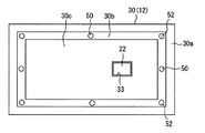
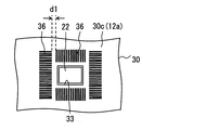
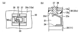
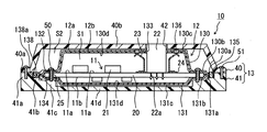
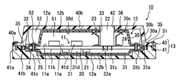
図1は、第1実施形態に係る電子装置の概略構成を示す平面図(第1ケース側から見た平面図)である。図2は、基板梱包具の概略構成を示す平面図(第1成形体側から見た平面図)である。図3は、図1のIII−III線に沿う断面図である。図4は、中継部材の概略構成を示す図であり、(a)は基板梱包具の外面側から見た平面図、b)は(a)のIVb−IVb線に沿う断面図である。なお、以下においては、回路基板の厚さ方向を単に厚さ方向とする。
Hereinafter, embodiments of the present invention will be described with reference to the drawings.
(First embodiment)
FIG. 1 is a plan view (plan view seen from the first case side) showing a schematic configuration of the electronic device according to the first embodiment. FIG. 2 is a plan view (plan view seen from the first molded body side) showing a schematic configuration of the substrate packing tool. 3 is a cross-sectional view taken along line III-III in FIG. 4A and 4B are diagrams illustrating a schematic configuration of the relay member, in which FIG. 4A is a plan view viewed from the outer surface side of the substrate packing tool, and FIG. 4B is a cross-sectional view taken along line IVb-IVb in FIG. In the following, the thickness direction of the circuit board is simply referred to as the thickness direction.

図1〜図3に示すように、電子装置10は、要部として、回路基板11と、内部空間S1に回路基板11を収容し、回路基板11を電磁波シールドする基板梱包具12と、を備えており、回路基板11には、回路基板11のGNDパターン(図示略)と基板梱包具12とを電気的に接続する接点ばね23が実装されている。本実施形態では、樹脂からなり、回路基板11を含む基板梱包具12を内部空間S2に収容する筐体13をさらに備えている。   As shown in FIGS. 1 to 3, the electronic device 10 includes, as main parts, a circuit board 11 and a board packaging 12 that houses the circuit board 11 in the internal space S <b> 1 and shields the circuit board 11 from electromagnetic waves. The circuit board 11 is mounted with a contact spring 23 for electrically connecting a GND pattern (not shown) of the circuit board 11 and the board packing tool 12. In the present embodiment, a housing 13 is further provided that is made of resin and accommodates the board packing tool 12 including the circuit board 11 in the internal space S2.

本実施形態に係る電子装置10は、自動車の計器(メータ)表示部の制御回路が回路基板11に構成されたメータ制御装置となっている。なお、上記計器表示部は、本実施形態において、図示しないLCDパネルにて構成されている。なお、内部空間S1が特許請求の範囲に記載の内部空間に相当する。   The electronic device 10 according to the present embodiment is a meter control device in which a control circuit of a vehicle meter display unit is configured on a circuit board 11. In addition, the said instrument display part is comprised with the LCD panel which is not illustrated in this embodiment. The internal space S1 corresponds to the internal space described in the claims.

回路基板11は、樹脂やセラミックスを主原料とする絶縁基材に、銅などの導電材料からなる配線(図示略)を配置してなる配線基板20を有している。本実施形態では、配線基板20として、ガラスエポキシ樹脂(ガラス繊維強化エポキシ樹脂)からなる絶縁基材に、銅箔をパターニングしてなる配線パターンが多層に配置された、平面矩形状の多層基板を採用している。   The circuit board 11 has a wiring board 20 in which wiring (not shown) made of a conductive material such as copper is disposed on an insulating base material mainly made of resin or ceramics. In the present embodiment, a planar rectangular multilayer substrate in which wiring patterns formed by patterning copper foil are arranged in multiple layers on an insulating base material made of glass epoxy resin (glass fiber reinforced epoxy resin) is used as the wiring substrate 20. Adopted.

この配線基板20の表裏面、換言すれば回路基板11の表面11a及び裏面11bには、上記配線の一部としてのランド(接点ばね23に対応するランド24以外については図示略)が複数設けられており、基板梱包具12との固定部位となる周縁部を除く中央部では、対応するランドに、マイコン、パワートランジスタ、抵抗、コンデンサなどの電子部品21がはんだ付け実装されている。本実施形態では、電子部品21のうち、アルミ電界コンデンサ(図示略)などの高背部品が表面11a側に実装され、高背部品よりも背の低い部品が裏面11b側に実装されている。そして、上記配線と電子部品21により、回路が構成されている。具体的には、回路基板11が、LCDパネルの制御回路として、LCDパネルの各画素を制御するLCDコントローラ及びCPU(CentralProcessing Unit)などを有している。それ以外にも、図示しないインターフェースやメモリなどを有している。なお、表面11aが第1主面に相当し、裏面11bが第2主面に相当する。   A plurality of lands (not shown except for the lands 24 corresponding to the contact springs 23) are provided on the front and back surfaces of the wiring board 20, in other words, on the front surface 11a and the back surface 11b of the circuit board 11. In the central part excluding the peripheral part which is a fixed part to the substrate packing tool 12, electronic parts 21 such as a microcomputer, a power transistor, a resistor, and a capacitor are soldered and mounted on the corresponding land. In the present embodiment, among the electronic components 21, a tall component such as an aluminum electric field capacitor (not shown) is mounted on the front surface 11a side, and a component shorter than the tall component is mounted on the back surface 11b side. The wiring and the electronic component 21 constitute a circuit. Specifically, the circuit board 11 has an LCD controller for controlling each pixel of the LCD panel, a CPU (Central Processing Unit), and the like as a control circuit for the LCD panel. In addition, it has an interface, a memory, etc. (not shown). The front surface 11a corresponds to the first main surface, and the back surface 11b corresponds to the second main surface.

回路基板11の表面11aには、上記したコネクタ22が、電源、GND、信号を入出力する機能、換言すれば回路基板11に構成された回路と外部機器とを電気的に接続する中継機能を果たすように、対応するランド(図示略)にはんだ付け実装されている。本実施形態では、一例として、コネクタ22と外部機器のコネクタ(図示略)との嵌合方向が、厚さ方向と一致しており、コネクタ22の端子22aが、厚さ方向に沿って配線基板20を貫通する挿入実装構造(フローはんだ付け実装構造)となっている。なお、コネクタ22としては、表面実装構造(リフローはんだ付け実装構造)のものを採用しても良い。   On the surface 11a of the circuit board 11, the above-described connector 22 has a function of inputting / outputting power, GND, and signals, in other words, a relay function of electrically connecting a circuit configured on the circuit board 11 and an external device. In order to fulfill, it is soldered and mounted on a corresponding land (not shown). In the present embodiment, as an example, the fitting direction of the connector 22 and a connector (not shown) of an external device coincides with the thickness direction, and the terminal 22a of the connector 22 is connected to the wiring board along the thickness direction. 20 is an insertion mounting structure that penetrates through 20 (flow soldering mounting structure). The connector 22 may have a surface mounting structure (reflow soldering mounting structure).

また、表面11aには、上記した接点ばね23が、配線基板20の配線のうち、GND電位に固定されたGNDパターン(図示略)と基板梱包具12とを電気的に接続するため、すなわち基板梱包具12をGND電位とするため、対応するランド24にはんだ付け実装されている。この接点ばね23は、ばね性を有するように金属板を所定形状に加工してなるものであり、基板梱包具12内に収容する前の状態における、厚さ方向の表面11aからの高さが、基板梱包具12内に回路基板11を収容した状態における、表面11aから基板梱包具12を構成する第1成形体30の内面30dまでの高さよりも低く設定されている。すなわち、基板梱包具12内に回路基板11を収容した状態で、接点ばね23は、第1成形体30の内面30dに、弾性変形した状態で接触するようになっている。   Further, the contact spring 23 described above is electrically connected to the surface 11a between the GND pattern (not shown) of the wiring of the wiring board 20 fixed to the GND potential and the board packing tool 12, that is, the board. In order to set the packing tool 12 to the GND potential, it is soldered and mounted on the corresponding land 24. The contact spring 23 is formed by processing a metal plate into a predetermined shape so as to have a spring property, and the height from the surface 11a in the thickness direction in a state before being accommodated in the substrate packing tool 12 is high. The height is set to be lower than the height from the surface 11 a to the inner surface 30 d of the first molded body 30 constituting the substrate packing tool 12 in a state where the circuit board 11 is accommodated in the substrate packing tool 12. That is, the contact spring 23 comes into contact with the inner surface 30d of the first molded body 30 in an elastically deformed state in a state in which the circuit board 11 is accommodated in the board packing tool 12.

特に本実施形態では、接点ばね23が、コネクタ22の周辺に配置されており、コネクタ22の複数の端子22aのうち、外部機器のシールド線と電気的に接続された一部の端子22aと、該端子22aに対応する回路基板11のランド、配線、上記ランド24を介して電気的に接続されている。すなわち、接点ばね23は、コネクタ22のシールドとなっており、外部からコネクタ22を介して回路基板11に侵入する外来ノイズ(電気ノイズ)を、GNDとしての基板梱包具12(第1成形体30の導電性織布12a)へ効果的に逃がす機能を果たすようになっている。   Particularly in the present embodiment, the contact spring 23 is disposed around the connector 22, and among the plurality of terminals 22 a of the connector 22, some of the terminals 22 a electrically connected to the shielded wire of the external device, The circuit board 11 corresponding to the terminal 22 a is electrically connected via the land, wiring, and the land 24. That is, the contact spring 23 serves as a shield for the connector 22, and external noise (electrical noise) that enters the circuit board 11 from the outside via the connector 22 is converted into GND by the substrate packing tool 12 (first molded body 30). The conductive woven fabric 12a) is effectively released.

さらに本実施形態では、接点ばね23が、コネクタ22を取り囲むように環状に配置されている。具体的には、コネクタ22のハウジング外面が図1及び図4(a)に示すように平面矩形状とされ、矩形をなす4つの外面それぞれに対応して、4つの接点ばね片23a〜23d(図4に接点ばね片23aを例示、接点ばね片23b〜23dは図示略)が設けられている。そして、隣り合う接点ばねの端部同士が溶接されて、環状の接点ばね23となっている。図1〜図4に示すように、基板梱包具12及び筐体13には、コネクタ22を外部に露出させるための貫通孔33,42がそれぞれ設けられているが、上記接点ばね23により、内部空間S1が閉じた空間となっている。すなわち、上記接点ばね23により、貫通孔33,42を介して出入する電磁波を、効果的にシールドすることができる。   Furthermore, in this embodiment, the contact spring 23 is annularly arranged so as to surround the connector 22. Specifically, the outer surface of the housing of the connector 22 has a planar rectangular shape as shown in FIGS. 1 and 4A, and four contact spring pieces 23a to 23d (corresponding to the four outer surfaces forming the rectangle). FIG. 4 illustrates contact spring pieces 23a, and contact spring pieces 23b to 23d are not shown. The ends of adjacent contact springs are welded to form an annular contact spring 23. As shown in FIGS. 1 to 4, the substrate packing tool 12 and the housing 13 are provided with through holes 33 and 42 for exposing the connector 22 to the outside. The space S1 is a closed space. That is, the contact spring 23 can effectively shield electromagnetic waves entering and exiting through the through holes 33 and 42.

また、本実施形態では、平面矩形状の回路基板11(配線基板20)における縁部に、基板梱包具12に回路基板11を固定するための螺子50,52の挿入される挿入孔25が、互いに離間して複数箇所に設けられている。本実施形態では、挿入孔25として、回路基板11とともに基板梱包具12を、筐体13を構成する第2ケース41に固定する螺子50用の4つの孔と、回路基板11を基板梱包具12に固定する螺子52用の4つの孔を有している。なお、螺子50用の4つの挿入孔25は、縁部における平面矩形状の回路基板11の各辺の中央にそれぞれ設けられ、螺子52用の4つの挿入孔25は、縁部における平面矩形状の回路基板11の4隅にそれぞれ設けられている(図2参照)。   Further, in the present embodiment, the insertion hole 25 into which the screws 50 and 52 for fixing the circuit board 11 to the board packing tool 12 are inserted at the edge of the planar rectangular circuit board 11 (wiring board 20). They are provided at a plurality of locations apart from each other. In the present embodiment, as the insertion holes 25, four holes for the screws 50 that fix the substrate packing tool 12 together with the circuit board 11 to the second case 41 constituting the housing 13, and the circuit board 11 to the board packing tool 12. There are four holes for the screw 52 to be fixed to. The four insertion holes 25 for the screws 50 are respectively provided at the centers of the sides of the planar rectangular circuit board 11 at the edges, and the four insertion holes 25 for the screws 52 are planar rectangular at the edges. Are provided at four corners of the circuit board 11 (see FIG. 2).

基板梱包具12は、上記したように、回路基板11を内部空間S1に収容し、回路基板11の電磁波シールドを行うものであり、本実施形態では、樹脂織布を金属メッキした導電性織布12aと樹脂織布からなる非導電性織布12b(金属メッキなし)との積層織布を成形してなる2つの成形体30,31により構成されており、非導電性織布12bが、基板梱包具12の内面30d,31dをなしている。なお、上記樹脂織布の原料としては、例えばポリエステル、特に高強度のポリエチレンテレフタレート(PET)、若しくはポリイミドを採用することができる。   As described above, the board packing tool 12 accommodates the circuit board 11 in the internal space S1 and performs electromagnetic wave shielding of the circuit board 11. In this embodiment, the conductive woven cloth obtained by metal plating the resin woven cloth is used. 12a and a non-conductive woven fabric 12b made of a resin woven fabric (non-metal plating) is formed by two molded bodies 30 and 31 formed by molding a non-conductive woven fabric 12b. Inner surfaces 30d and 31d of the packing tool 12 are formed. In addition, as a raw material of the said resin woven fabric, polyester, especially high-strength polyethylene terephthalate (PET), or a polyimide can be employ | adopted, for example.

また、2つの成形体30,31は、接着剤(図示略)を介して導電性織布12aと非導電性織布12bを積層配置し、圧空成形することで、それぞれ形成されている。このような成形体30,31は、外力の印加がない限り所定形状を維持するが、外力が印加されると、多少なりとも変形する柔軟性を有している。例えば成形体30,31の厚さが、0.1mm以上、5mm以下の範囲にあることが好ましい。成形体30,31の厚さが0.1mmより薄い場合には、所定形状を維持するための強度が不足し、成形体30,31の厚さが5mmより大きい場合には、基板梱包具12が従来の樹脂筐体と同程度の重量となってしまう。さらには、成形体30,31の厚さが、0.3mm以上、1.5mm以下の範囲にあることが好ましい。成形体30,31の厚さが0.3mmより薄い場合には、成形体30,31を組み付ける場合に曲げてしまうおそれがあり、成形体30,31の厚さが1.5mmより大きい場合には、加圧した時の厚さ方向の変形量も大きいため、例えば螺子50による固定作業がやりずらくなる。   The two molded bodies 30 and 31 are respectively formed by laminating and arranging the conductive woven fabric 12a and the non-conductive woven fabric 12b via an adhesive (not shown) and pressure forming. Such molded bodies 30 and 31 maintain a predetermined shape as long as no external force is applied, but have a flexibility to be deformed to some extent when an external force is applied. For example, the thicknesses of the molded bodies 30 and 31 are preferably in the range of 0.1 mm or more and 5 mm or less. When the thickness of the molded bodies 30 and 31 is less than 0.1 mm, the strength for maintaining the predetermined shape is insufficient, and when the thickness of the molded bodies 30 and 31 is greater than 5 mm, the substrate packing 12 However, it becomes the same weight as the conventional resin casing. Furthermore, it is preferable that the thickness of the molded bodies 30 and 31 is in the range of 0.3 mm or more and 1.5 mm or less. When the thickness of the molded bodies 30 and 31 is less than 0.3 mm, there is a risk of bending when the molded bodies 30 and 31 are assembled. When the thickness of the molded bodies 30 and 31 is greater than 1.5 mm Since the amount of deformation in the thickness direction when pressurized is large, for example, fixing work by the screw 50 becomes difficult.

2つの成形体30,31のうち、第1成形体30は、主として回路基板11の表面11a側を覆う部位であり、第2成形体31は、主として回路基板11の裏面11b側を覆う部位である。そして、2つの成形体30,31を厚さ方向に沿って組み付けることで、回路基板11を収容する内部空間S1を備えた基板梱包具12となっている。本実施形態では、2つの成形体30,31の平面形状(厚さ方向に垂直な平面形状)が、回路基板11の平面形状(平面矩形状)に対応してともに矩形状とされている。そして、環状の縁部30a,31aを互いに重ね合わせた(内面30d,31d同士を接触させた)状態で、縁部30a,31a全周に亘り、図3に示すように、縁部30a,31a同士を導電糸35で縫い合わせることで、端部が閉じた袋状の基板梱包具12となっている。換言すれば、導電糸35により、縁部30a,31a全周に亘って、第1成形体30の外面をなす導電性織布12aと、第2成形体31の外面をなす導電性織布12aとが電気的に接続され、これにより、基板梱包具12が、内部空間S1に収容された回路基板11に対して略全方位の電磁波シールドを行うようになっている。なお、本実施形態では、縁部30a,31a全周に亘って、導電糸35が密に(隙間無く)縫われている。   Of the two molded bodies 30, 31, the first molded body 30 is a part that mainly covers the front surface 11 a side of the circuit board 11, and the second molded body 31 is a part that mainly covers the back surface 11 b side of the circuit board 11. is there. Then, by assembling the two molded bodies 30 and 31 along the thickness direction, the substrate packaging tool 12 having the internal space S1 for accommodating the circuit board 11 is obtained. In the present embodiment, the planar shapes (planar shapes perpendicular to the thickness direction) of the two molded bodies 30 and 31 are both rectangular corresponding to the planar shape (planar rectangular shape) of the circuit board 11. Then, in a state where the annular edge portions 30a and 31a are overlapped with each other (the inner surfaces 30d and 31d are in contact with each other), as shown in FIG. 3, the edge portions 30a and 31a over the entire circumference of the edge portions 30a and 31a. By stitching them together with the conductive thread 35, the bag-like substrate packing tool 12 with the closed end is formed. In other words, the conductive woven fabric 12a that forms the outer surface of the first molded body 30 and the conductive woven fabric 12a that forms the outer surface of the second molded body 31 are formed by the conductive yarn 35 over the entire periphery of the edges 30a and 31a. Are electrically connected to each other, so that the substrate packing 12 performs electromagnetic wave shielding in almost all directions with respect to the circuit board 11 accommodated in the internal space S1. In the present embodiment, the conductive yarn 35 is sewn densely (without a gap) over the entire periphery of the edges 30a and 31a.

第1成形体30は、環状の縁部30aと、縁部30aに囲まれた中央部を有しており、中央部が縁部30aに対して凹んでいる。そして、この凹部(中央部)として、縁部30aに連なっており、回路基板11を内部空間S1に収容した状態で、凹部底面(内面30d)の少なくとも一部が、回路基板11の表面11aと接触する第1凹部30bと、第1凹部30bよりも凹部底面(内面)と回路基板11の表面11aとの対向距離が長い第2凹部30cを有している。すなわち、凹部が、縁部30aを基準として深さの異なる2つの凹部30b,30cを有する2段構造となっている。   The first molded body 30 has an annular edge portion 30a and a center portion surrounded by the edge portion 30a, and the center portion is recessed with respect to the edge portion 30a. And as this recessed part (center part), it continues to the edge part 30a, and in the state which accommodated the circuit board 11 in internal space S1, at least one part of a recessed part bottom face (inner surface 30d) is the surface 11a of the circuit board 11, and The first recess 30b is in contact, and the second recess 30c has a longer distance between the bottom surface (inner surface) of the recess and the surface 11a of the circuit board 11 than the first recess 30b. That is, the concave portion has a two-stage structure having two concave portions 30b and 30c having different depths with respect to the edge portion 30a.

第1凹部30bは、回路基板11を内部空間S1に収容した状態で、回路基板11における表面11a側の縁部と対向する部位であり、第2成形体31の対応する第1凹部31bとの間で、回路基板11を挟んで固定するようになっている。本実施形態では、第1凹部30bに、螺子50,52が挿入される挿入孔32が、上記した挿入孔25に対応して設けられている。   The first recess 30b is a portion facing the edge on the surface 11a side of the circuit board 11 in a state in which the circuit board 11 is accommodated in the internal space S1, and with the corresponding first recess 31b of the second molded body 31. Between them, the circuit board 11 is sandwiched and fixed. In the present embodiment, an insertion hole 32 into which the screws 50 and 52 are inserted is provided in the first recess 30 b corresponding to the above-described insertion hole 25.

第2凹部30cは、回路基板11を内部空間S1に収容した状態で、回路基板11の表面11aに実装された電子部品21と接触せず、且つ、接点ばね23が内面30dに接触するように、所定の深さを有している。本実施形態では、第2凹部30cに、コネクタ22を外部に露出させるための貫通孔33が形成されている。また、接点ばね23に対応して、接点ばね23と導電性織布12aとの電気的な接続を中継する中継部材36も固定されている。   The second recess 30c does not contact the electronic component 21 mounted on the surface 11a of the circuit board 11 in a state where the circuit board 11 is accommodated in the internal space S1, and the contact spring 23 contacts the inner surface 30d. , Has a predetermined depth. In the present embodiment, a through-hole 33 for exposing the connector 22 to the outside is formed in the second recess 30c. Corresponding to the contact spring 23, a relay member 36 that relays the electrical connection between the contact spring 23 and the conductive woven fabric 12a is also fixed.

中継部材36は導電材料からなり、基板梱包具12の外面をなす導電性織布12aのうち、接点ばね23が固定された回路基板11の表面11aを覆う部位、すなわち第1成形体30の導電性織布12aと電気的に接続されるとともに、内面30dをなす非導電性織布12bの表面において接点ばね23の接触部位に配置されている。本実施形態では、中継部材36が、図4(a),(b)に示すように、導電性を有する導電糸により構成されており、貫通孔33を取り囲んで第2凹部30cに固定されている。具体的には、第2凹部30cにおける貫通孔33の周囲において、導電性織布12aと非導電性織布12bとを縫い合わせることで、導電糸からなる中継部材36が第2凹部30cに固定されている。なお、本実施形態では、図4(a)に示すように、貫通孔33を取り囲んで、導電糸35が密に(隙間無く)縫われている。そして、組み付け状態で、非導電性織布12bの表面に配置された継部材36と接点ばね23とが、コネクタ22を取り囲んで互いに接触している。   The relay member 36 is made of a conductive material, and a portion of the conductive woven fabric 12 a that forms the outer surface of the substrate packing tool 12 that covers the surface 11 a of the circuit board 11 to which the contact spring 23 is fixed, that is, the conductivity of the first molded body 30. In addition to being electrically connected to the conductive woven fabric 12a, it is disposed at the contact portion of the contact spring 23 on the surface of the non-conductive woven fabric 12b forming the inner surface 30d. In the present embodiment, as shown in FIGS. 4A and 4B, the relay member 36 is made of conductive thread having conductivity, and is fixed to the second recess 30c surrounding the through hole 33. Yes. Specifically, the relay member 36 made of conductive yarn is fixed to the second recess 30c by sewing the conductive woven fabric 12a and the non-conductive woven fabric 12b around the through hole 33 in the second recess 30c. ing. In the present embodiment, as shown in FIG. 4A, the conductive thread 35 is sewn densely (without a gap) so as to surround the through hole 33. In the assembled state, the joint member 36 and the contact spring 23 disposed on the surface of the non-conductive woven fabric 12b surround the connector 22 and are in contact with each other.

一方、第2成形体31も、環状の縁部31aと、縁部31aに囲まれた中央部を有しており、中央部が縁部31aに対して凹んでいる。そして、この凹部(中央部)として、縁部31aに連なっており、回路基板11を内部空間S1に収容した状態で、凹部底面(内面30d)の少なくとも一部が、回路基板11の裏面11bと接触する第1凹部31bと、第1凹部31bよりも凹部底面(内面)と回路基板11の裏面11bとの対向距離が長い第2凹部31cを有している。すなわち、凹部が、縁部31aを基準として深さの異なる2つの凹部31b,31cを有する2段構造となっている。   On the other hand, the 2nd molded object 31 also has the cyclic | annular edge part 31a and the center part enclosed by the edge part 31a, and the center part is dented with respect to the edge part 31a. And as this recessed part (center part), it continues to the edge part 31a, and in the state which accommodated the circuit board 11 in internal space S1, at least one part of a recessed part bottom face (inner surface 30d) is with the back surface 11b of the circuit board 11 The first recess 31b is in contact with the first recess 31b, and the second recess 31c has a longer facing distance between the bottom surface (inner surface) of the recess and the back surface 11b of the circuit board 11 than the first recess 31b. That is, the recess has a two-stage structure having two recesses 31b and 31c having different depths with respect to the edge 31a.

第1凹部31bは、上記した第1凹部30bに対応しており、回路基板11を内部空間S1に収容した状態で、回路基板11における裏面11b側の縁部と対向し、第1凹部30bとの間に回路基板11を挟んで固定するようになっている。この第1凹部31bには、螺子50,52が挿入される挿入孔34が、上記した挿入孔25に対応して設けられている。なお、螺子52が挿入される挿入孔34は、螺子52が螺合される螺子孔となっている。   The first recess 31b corresponds to the first recess 30b described above, and faces the edge on the back surface 11b side of the circuit board 11 in a state where the circuit board 11 is accommodated in the internal space S1, and the first recess 30b The circuit board 11 is sandwiched between and fixed. In the first recess 31b, an insertion hole 34 into which the screws 50 and 52 are inserted is provided corresponding to the insertion hole 25 described above. The insertion hole 34 into which the screw 52 is inserted is a screw hole into which the screw 52 is screwed.

第2凹部31cは、上記した第2凹部30cに対応しており、回路基板11を内部空間S1に収容した状態で、回路基板11の裏面11bに実装された電子部品21と接触しないように、所定の深さを有している。本実施形態では、上記したように、電子部品21のうちの高背部品を表面11aに実装しているため、第2凹部31cの深さが、第1成形体30側の第2凹部30cの深さよりも浅くなっている。   The second recess 31c corresponds to the second recess 30c described above, and in a state where the circuit board 11 is accommodated in the internal space S1, the second recess 31c does not come into contact with the electronic component 21 mounted on the back surface 11b of the circuit board 11. It has a predetermined depth. In the present embodiment, as described above, since the tall component of the electronic component 21 is mounted on the surface 11a, the depth of the second recess 31c is the depth of the second recess 30c on the first molded body 30 side. It is shallower than the depth.

筐体13は、樹脂材料からなり、回路基板11に対して主として表面11a側に配置される第1ケース40と、主として裏面11b側に配置される第2ケース41とにより、厚さ方向に開閉可能に構成されている。そして、第1ケース40と第2ケース41を厚さ方向に沿って組み付けることで、回路基板11を含む基板梱包具12を収容する内部空間S2を備えた筐体13となっている。このように、筐体13は、回路基板11を含む基板梱包具12を保護するものである。なお、筐体13を構成する樹脂材料としては、エポキシ樹脂など周知の材料を採用することができる。   The housing 13 is made of a resin material, and is opened and closed in the thickness direction by a first case 40 disposed mainly on the front surface 11a side and a second case 41 disposed mainly on the back surface 11b side with respect to the circuit board 11. It is configured to be possible. And the 1st case 40 and the 2nd case 41 are assembled | attached along the thickness direction, and it becomes the housing | casing 13 provided with the interior space S2 which accommodates the board | substrate packing tool 12 containing the circuit board 11. FIG. As described above, the housing 13 protects the board packing tool 12 including the circuit board 11. In addition, as a resin material which comprises the housing | casing 13, well-known materials, such as an epoxy resin, are employable.

本実施形態では、第1ケース40及び第2ケース41が、分離可能に構成(別部材として構成)されている。また、2つのケース40,41の平面形状(厚さ方向に垂直な平面形状)が、平面矩形状の回路基板11及び基板梱包具12に対応して、ともに矩形状とされており、互いに対応する環状の縁部40a,41aには、螺子51が螺合される複数の螺子孔(図示略)がそれぞれ設けられている。そして、環状の縁部40a,41aを互いに重ね合わせた状態で、一致する螺子孔(図示略)に螺子51を螺合させることで、1つの筐体13が構成されるようになっている。なお、図1に示すように、本実施形態では、螺子51による固定部位が、ほぼ等間隔で10箇所設けられている。   In the present embodiment, the first case 40 and the second case 41 are configured to be separable (configured as separate members). In addition, the planar shapes (planar shapes perpendicular to the thickness direction) of the two cases 40 and 41 are both rectangular, corresponding to the planar rectangular circuit board 11 and the substrate packing tool 12, and correspond to each other. A plurality of screw holes (not shown) into which the screws 51 are screwed are provided in the annular edges 40a and 41a. Then, one casing 13 is configured by screwing a screw 51 into a matching screw hole (not shown) in a state where the annular edges 40a and 41a are overlapped with each other. As shown in FIG. 1, in the present embodiment, ten fixing portions by the screws 51 are provided at approximately equal intervals.

第1ケース40の縁部40aは、図3に示すように、第2ケース41の縁部41aと対向している。また、環状の縁部40aに囲まれた中央部が凹部40bとなっている。凹部40bは、基板梱包具12における第1成形体30側を収容すべく、所定の深さを有している。本実施形態では、コネクタ22を外部に露出させるための貫通孔42が、凹部40bに形成されている。なお、第1ケース40の凹部40bが、第1成形体30の第2凹部30cと接触する構成としても良いが、本実施形態では、凹部40bと第2凹部30cとの間に隙間を有する構成となっている。   The edge part 40a of the 1st case 40 is facing the edge part 41a of the 2nd case 41, as shown in FIG. Moreover, the center part enclosed by the annular edge part 40a becomes the recessed part 40b. The recess 40b has a predetermined depth so as to accommodate the first molded body 30 side in the substrate packing tool 12. In the present embodiment, a through hole 42 for exposing the connector 22 to the outside is formed in the recess 40b. In addition, although it is good also as a structure which the recessed part 40b of the 1st case 40 contacts the 2nd recessed part 30c of the 1st molded object 30, in this embodiment, a structure which has a clearance gap between the recessed part 40b and the 2nd recessed part 30c. It has become.

一方、第2ケース41でも、環状の縁部41aに囲まれた中央部が凹部となっており、凹部として、縁部41aに連なっており、第2成形体31の縁部31aと対向する第1凹部41bと、第1凹部41bよりも深く、第2成形体31の第1凹部31b(換言すれば、回路基板11の周縁部)と対向する第2凹部41cと、第2凹部41cよりも深く、第2成形体31の第2凹部31cと対向する第3凹部41dを有している。すなわち、凹部が、縁部41aを基準として深さの異なる3つの凹部41b,41c,41dを有する3段構造となっている。   On the other hand, also in the second case 41, the central part surrounded by the annular edge part 41a is a concave part, and the concave part continues to the edge part 41a and faces the edge part 31a of the second molded body 31. 1 recessed part 41b, 2nd recessed part 41c which is deeper than 1st recessed part 41b, and opposes 1st recessed part 31b (in other words, peripheral part of the circuit board 11) of the 2nd molded object 31, and 2nd recessed part 41c Deeply, it has the 3rd recessed part 41d facing the 2nd recessed part 31c of the 2nd molded object 31. As shown in FIG. That is, the concave portion has a three-stage structure having three concave portions 41b, 41c, and 41d having different depths with respect to the edge portion 41a.

第1凹部41bは、上記したように第2成形体31の縁部31aと対向しており、基板梱包具12において、導電糸35により縫い合わされた部位を含む縁部30a,31aを支持するようになっている。   As described above, the first concave portion 41 b faces the edge portion 31 a of the second molded body 31, and supports the edge portions 30 a and 31 a including the portion stitched by the conductive thread 35 in the substrate packing tool 12. It has become.

第2凹部41cは、上記したように第2成形体31の第1凹部31bと対向しており、基板梱包具12における各成形体30,31の第1凹部30b,31b及び回路基板11の周縁部を支持するようになっている。また、本実施形態では、第2凹部41cに、上記した挿入孔25,32,34のうちの螺子50用の挿入孔に対応して、螺子孔(図示略)が設けられている。そして、第2凹部41c上に、第2成形体31、回路基板11、第1成形体30の順に積層配置した状態で、互いに重なり合う上記4つの孔に螺子50を螺合させることで、回路基板11を2つの成形体30,31に固定するとともに、回路基板11を収容した基板梱包具12を第2ケース41(筐体13)に固定するようになっている。   As described above, the second concave portion 41 c faces the first concave portion 31 b of the second molded body 31, and the first concave portions 30 b and 31 b of the molded bodies 30 and 31 and the peripheral edge of the circuit board 11 in the substrate packing tool 12. Supporting the part. In the present embodiment, screw holes (not shown) are provided in the second recess 41c corresponding to the insertion holes for the screws 50 among the insertion holes 25, 32, and 34 described above. Then, in the state where the second molded body 31, the circuit board 11, and the first molded body 30 are stacked in this order on the second recess 41c, the screw 50 is screwed into the four holes that overlap each other, whereby the circuit board is obtained. 11 is fixed to the two molded bodies 30 and 31, and the board packaging 12 containing the circuit board 11 is fixed to the second case 41 (housing 13).

第3凹部41dは、上記したように第2成形体31の第2凹部31cと対向、すなわち回路基板11の中央部と対向しており、基板梱包具12における第2成形体31側を収容すべく、所定の深さを有している。なお、第2ケース40の第3凹部41dが、第2成形体31の第2凹部31cと接触する構成としても良いが、本実施形態では、第3凹部41dと第2凹部31cとの間に隙間を有する構成となっている。   As described above, the third recessed portion 41d faces the second recessed portion 31c of the second molded body 31, that is, faces the central portion of the circuit board 11, and accommodates the second molded body 31 side of the substrate packing tool 12. Therefore, it has a predetermined depth. In addition, although it is good also as a structure which the 3rd recessed part 41d of the 2nd case 40 contacts with the 2nd recessed part 31c of the 2nd molded object 31, in this embodiment, it is between the 3rd recessed part 41d and the 2nd recessed part 31c. It has a configuration with a gap.

次に、上記した電子装置10の組み付け方法について、図3を用いて説明する。先ず、回路基板11、成形体30,31、ケース40,41をそれぞれ準備する。この時点で、回路基板11には、電子部品21とともに、コネクタ22、接点ばね23も実装されている。   Next, a method for assembling the electronic device 10 will be described with reference to FIG. First, the circuit board 11, the molded bodies 30, 31, and the cases 40, 41 are prepared. At this time, the connector 22 and the contact spring 23 are mounted on the circuit board 11 together with the electronic component 21.

次いで、回路基板11を基板梱包具12に固定する。先ず、第2成形体31上に、回路基板11を位置決め載置する。このとき、第1凹部31b上に回路基板11の周縁部が位置し、第1凹部31bに設けられた挿入孔34に、対応する挿入孔25が一致するように載置する。次に、回路基板11の表面11aを覆うように、第2成形体31及び回路基板11上に第1成形体30を位置決め載置する。このとき、第2成形体31の縁部31a上に第1成形体30の縁部30aが位置し、回路基板11の周縁部上に第1凹部30bが位置し、回路基板11の挿入孔25に、対応する挿入孔32が一致し、コネクタ22が第2凹部30cの貫通孔33を挿通するように載置する。そして、この状態で、挿入孔25,32,34のうち、螺子52に対応する4隅部の挿入孔25,32,34に螺子52をそれぞれ挿入し、成形体30,31に回路基板11を固定する。この状態で、接点ばね23は中継部材36に接触する。   Next, the circuit board 11 is fixed to the board packing tool 12. First, the circuit board 11 is positioned and placed on the second molded body 31. At this time, the peripheral portion of the circuit board 11 is positioned on the first recess 31b, and the circuit board 11 is placed so that the corresponding insertion hole 25 coincides with the insertion hole 34 provided in the first recess 31b. Next, the first molded body 30 is positioned and placed on the second molded body 31 and the circuit board 11 so as to cover the surface 11 a of the circuit board 11. At this time, the edge 30 a of the first molded body 30 is located on the edge 31 a of the second molded body 31, the first recess 30 b is located on the peripheral edge of the circuit board 11, and the insertion hole 25 of the circuit board 11. The corresponding insertion holes 32 are aligned with each other, and the connector 22 is placed so as to pass through the through hole 33 of the second recess 30c. In this state, among the insertion holes 25, 32, and 34, the screws 52 are respectively inserted into the insertion holes 25, 32, and 34 at the four corners corresponding to the screws 52, and the circuit board 11 is inserted into the molded bodies 30 and 31, respectively. Fix it. In this state, the contact spring 23 contacts the relay member 36.

次に、2つの成形体30,31の縁部30a,31aを互いに重ね合わせた状態で、縁部30a,31a同士を導電糸35で縫い合わせる。本実施形態では、環状の縁部30a,31a全周に亘って、密に(隙間無く)縫い合わせる。これにより、端部が閉じた袋状の基板梱包具12が得られる。なお、基板梱包具12を得た状態で、回路基板11は基板梱包具12に固定されるとともに、その内部空間S1に収容されている。   Next, in a state where the edges 30 a and 31 a of the two molded bodies 30 and 31 are overlapped with each other, the edges 30 a and 31 a are stitched together with the conductive thread 35. In the present embodiment, the entire edges of the annular edges 30a and 31a are sewn tightly (no gaps). Thereby, the bag-shaped board | substrate packing tool 12 with which the edge part was closed is obtained. In addition, the circuit board 11 is fixed to the board packaging tool 12 in the state where the board packaging tool 12 is obtained, and is accommodated in the internal space S1.

次に、基板梱包具12を第2ケース41に固定する。先ず、第2ケース41の第1凹部41b上に、成形体30,31の縁部30a,31aが位置し、第2凹部41c上に、成形体30,31の第1凹部30b,31b及び回路基板11の周縁部が位置し、第2ケース41の螺子孔が、対応する螺子50用の挿入孔25,32,34と一致するように、基板梱包具12を、第2成形体31側を搭載側として第2ケース41に位置決め載置する。そして、この状態で、螺子50に対応する挿入孔25,32,34及び螺子孔に螺子50をそれぞれ挿入し、基板梱包具12を第2ケース41に固定する。   Next, the substrate packing tool 12 is fixed to the second case 41. First, the edges 30a and 31a of the molded bodies 30 and 31 are positioned on the first recess 41b of the second case 41, and the first recesses 30b and 31b of the molded bodies 30 and 31 and the circuit are positioned on the second recess 41c. The substrate packing tool 12 is placed on the second molded body 31 side so that the peripheral edge of the substrate 11 is located and the screw holes of the second case 41 are aligned with the corresponding insertion holes 25, 32, 34 for the screws 50. It is positioned and placed on the second case 41 as the mounting side. Then, in this state, the screws 50 are respectively inserted into the insertion holes 25, 32, 34 and the screw holes corresponding to the screws 50, and the substrate packing tool 12 is fixed to the second case 41.

次に、第1ケース40を第2ケース41に組み付ける。先ず、第2ケースの縁部41a上に、第1ケース40の縁部40aが位置し、縁部40a,41aの対応する螺子孔(図示略)が一致し、コネクタ22が凹部40bの貫通孔42を挿通するように、第2ケース41に第1ケース40を位置決め載置する。そして、この状態で、螺子51により、第1ケース40を第2ケース41に組み付ける。以上により、上記した電子装置10を得ることができる。   Next, the first case 40 is assembled to the second case 41. First, the edge 40a of the first case 40 is positioned on the edge 41a of the second case, the corresponding screw holes (not shown) of the edges 40a and 41a are aligned, and the connector 22 is a through hole of the recess 40b. The first case 40 is positioned and placed on the second case 41 so as to be inserted through the second case 41. In this state, the first case 40 is assembled to the second case 41 with the screw 51. Thus, the electronic device 10 described above can be obtained.

次に、本実施形態に係る電子装置10の特徴部分の効果について説明する。先ず本実施形態では、樹脂織布を金属メッキした導電性織布12aと樹脂織布からなる非導電性織布12bとの積層織布の成形体30,31により、基板梱包具12が構成されている。すなわち、基板梱包具12の主材料が樹脂織布となっている。また、筐体13も樹脂材料からなる。したがって、従来の金属筐体に比べて、電子装置10を軽量化することができる。   Next, the effect of the characteristic part of the electronic device 10 according to the present embodiment will be described. First, in this embodiment, the substrate packing tool 12 is constituted by the laminated woven fabric molded bodies 30 and 31 of the conductive woven fabric 12a obtained by metal plating the resin woven fabric and the non-conductive woven fabric 12b made of the resin woven fabric. ing. That is, the main material of the substrate packing tool 12 is a resin woven fabric. The housing 13 is also made of a resin material. Therefore, the electronic device 10 can be reduced in weight as compared with the conventional metal casing.

また、基板梱包具12において、非導電性織布12bが内面30d,31dをなしているので、回路基板11に構成された回路(電子部品21や配線)のうちのGND電位に固定される部位を除く部位と、基板梱包具12とのショートを防ぐことができる。   Moreover, in the board | substrate packing tool 12, since the nonelectroconductive woven fabric 12b has comprised inner surface 30d and 31d, the site | part fixed to GND electric potential among the circuits (electronic component 21 and wiring) comprised in the circuit board 11 It is possible to prevent a short circuit between the portion except for and the substrate packing tool 12.

また、非導電性織布12bが基板梱包具12の内面30d,31dをなしているので、製造途中、特に回路基板11を基板梱包具12の内部空間S1に収容する際に、回路基板11に実装された電子部品21が導電性織布12aに接触しがたく、導電性織布12aにおける金属メッキ層の剥がれを抑制することができる。なお、導電性織布12aは、樹脂織布を金属メッキしたもので、金属メッキされた樹脂繊維が立体的に絡み合った構造となっている。すなわち、導電性織布12aを含む成形体30,31の金属メッキ層は、従来の樹脂筐体に設けられた導電性層(内面メッキ層)のような筐体表面にだけあるものではない。したがって、製造途中に擦れ等があっても、導電性織布12aからなる成形体30,31の金属メッキ層のうち、その厚さ方向の一部(例えば表面のみ)が剥がれる程度であり、電磁波シールドの効果を維持することができる。   In addition, since the non-conductive woven fabric 12b forms the inner surfaces 30d and 31d of the board packaging tool 12, the circuit board 11 is placed on the circuit board 11 during manufacturing, particularly when the circuit board 11 is accommodated in the internal space S1 of the board packaging tool 12. The mounted electronic component 21 is unlikely to contact the conductive woven fabric 12a, and peeling of the metal plating layer on the conductive woven fabric 12a can be suppressed. The conductive woven fabric 12a is obtained by metal-plating a resin woven fabric, and has a structure in which metal-plated resin fibers are entangled three-dimensionally. That is, the metal plating layers of the molded bodies 30 and 31 including the conductive woven fabric 12a are not only on the surface of the casing such as the conductive layer (inner plating layer) provided on the conventional resin casing. Therefore, even if rubbing or the like occurs in the course of manufacture, a part (for example, only the surface) in the thickness direction of the metal plating layers of the molded bodies 30 and 31 made of the conductive woven fabric 12a is peeled off, and the electromagnetic wave The effect of the shield can be maintained.

また、導電性の中継部材36が、基板梱包具12の外面をなす導電性織布12aと電気的に接続されるとともに、基板梱包具12の内面30d,31dをなす非導電性織布12bの表面において接点ばね23の接触部位に配置されている。したがって、非導電性織布12bが基板梱包具12の内面30d、31dをなす構成でありながら、接点ばね23の弾性変形により、回路基板11のGNDパターンと基板梱包具12(導電性織布12a)との電気的接続状態を良好に確保することができる。すなわち、基板梱包具12と接点ばね23がGND電位に固定されるので、基板梱包具12(及び接点ばね23)を電磁波シールドとして効果的に機能させることができる。   In addition, the conductive relay member 36 is electrically connected to the conductive woven fabric 12a that forms the outer surface of the substrate packaging tool 12, and the non-conductive woven fabric 12b that forms the inner surfaces 30d and 31d of the substrate packaging tool 12. It is arrange | positioned in the contact site | part of the contact spring 23 in the surface. Accordingly, the non-conductive woven fabric 12b forms the inner surfaces 30d and 31d of the substrate packing 12, and the elastic deformation of the contact spring 23 causes the GND pattern of the circuit board 11 and the substrate packing 12 (conductive woven fabric 12a). ) Can be secured well. That is, since the substrate packaging tool 12 and the contact spring 23 are fixed to the GND potential, the substrate packaging tool 12 (and the contact spring 23) can effectively function as an electromagnetic wave shield.

以上から、本実施形態に係る電子装置10によれば、軽量で、回路基板11とのショートを防ぎつつ電磁波シールド効果を確保することができる。なお、接点ばね23も電磁波シールドとして機能するので、コネクタ22用の貫通孔33,42を介して内部空間S1に出入りする電磁波を効果的にシールドすることができる。   From the above, according to the electronic device 10 according to the present embodiment, it is lightweight and can secure an electromagnetic wave shielding effect while preventing a short circuit with the circuit board 11. Since the contact spring 23 also functions as an electromagnetic wave shield, it is possible to effectively shield electromagnetic waves that enter and exit the internal space S1 through the through holes 33 and 42 for the connector 22.

また、本実施形態では、中継部材36として、導電性を有する導電糸を採用しており、導電糸により、導電性織布12aと非導電性織布12bとを縫い合わせている。したがって、中継部材36を積層織布に固定するための貫通孔が不要であるので、製造工程を簡素化し、製造コストを低減することができる。また、積層織布に貫通孔を設けなくとも良いので、電磁波シールド効果を高めることもできる。   Moreover, in this embodiment, the conductive yarn which has electroconductivity is employ | adopted as the relay member 36, and the electroconductive woven fabric 12a and the nonelectroconductive woven fabric 12b are stitched together by the electroconductive yarn. Accordingly, since a through hole for fixing the relay member 36 to the laminated woven fabric is unnecessary, the manufacturing process can be simplified and the manufacturing cost can be reduced. Moreover, since it is not necessary to provide a through-hole in the laminated woven fabric, the electromagnetic wave shielding effect can be enhanced.

また、本実施形態では、接点ばね23が、コネクタ22の周辺に配置されており、コネクタ22の複数の端子22aのうち、外部機器のシールド線と電気的に接続された一部の端子22aと、該端子22aに対応する回路基板11のランド、配線、ランド24を介して電気的に接続されている。すなわち、接点ばね23がコネクタ22のシールドとなっており、外部からコネクタ22を介して回路基板11に侵入する外来ノイズを、GNDとしての基板梱包具12(第1成形体30)へ効果的に逃がすことができる。   In the present embodiment, the contact spring 23 is disposed around the connector 22, and among the plurality of terminals 22 a of the connector 22, some of the terminals 22 a electrically connected to the shield wire of the external device The circuit board 11 corresponding to the terminal 22a is electrically connected via the land, wiring, and land 24. That is, the contact spring 23 serves as a shield for the connector 22, and external noise that enters the circuit board 11 from the outside via the connector 22 is effectively applied to the board packing tool 12 (first molded body 30) as GND. I can escape.

また、本実施形態では、コネクタ22の周囲に接点ばね23を設けるので、貫通孔33,42を有しながらも、接点ばね23により内部空間S1が閉じた空間となっており、接点ばね23により、コネクタ22用の貫通孔33,42を介して内部空間S1に出入りする電磁波をより効果的にシールドすることができる。さらには、コネクタの近傍にランド24及び接点ばね23を設けるので、接点ばね23をコネクタ22とは離れた位置に設ける構成に比べて、基板梱包具12及び接点ばね23による内部空間S1内において、電子部品21の実装スペースを広く確保することができる。   In the present embodiment, since the contact spring 23 is provided around the connector 22, the inner space S <b> 1 is closed by the contact spring 23 while having the through holes 33 and 42. Electromagnetic waves entering and exiting the internal space S1 through the through holes 33 and 42 for the connector 22 can be shielded more effectively. Furthermore, since the land 24 and the contact spring 23 are provided in the vicinity of the connector, compared to the configuration in which the contact spring 23 is provided at a position away from the connector 22, the internal space S1 by the board packing tool 12 and the contact spring 23 is A wide mounting space for the electronic component 21 can be secured.

また、本実施形態では、基板梱包具12が2つの成形体30,31からなるので、回路基板11を収容すべく所定形状及び大きさの内部空間S1を確保し、回路基板11と基板梱包具12との接触を抑制することができる。これにより、例えば回路基板の電子部品21と基板梱包具12との接触を避けて、電子部品21の接続信頼性を向上することができる。   Moreover, in this embodiment, since the board | substrate packing tool 12 consists of the two molded objects 30,31, the internal space S1 of a predetermined shape and a size is ensured so that the circuit board 11 may be accommodated, and the circuit board 11 and a board | substrate packing tool. 12 can be suppressed. Thereby, the contact reliability of the electronic component 21 of a circuit board and the board | substrate packing tool 12, for example can be avoided, and the connection reliability of the electronic component 21 can be improved.

また、本実施形態では、成形体30,31が、圧空成形により形成されている。このように圧空成形法を用いると、成形体30,31を、肉薄軽量で安価に製造することができる。しかしながら、圧空成形以外にも、真空成形や、熱プレスなどを採用することもできる。   In the present embodiment, the molded bodies 30 and 31 are formed by pressure forming. When the compressed air molding method is used in this way, the molded bodies 30 and 31 can be manufactured thin and lightweight at low cost. However, in addition to pressure forming, vacuum forming, hot pressing, or the like can be employed.

なお、本実施形態では、接点ばね23及び中継部材36が、コネクタ22を取り囲む環状とされる例を示したが、複数の、接点ばね23及び中継部材36としても良い。換言すれば、隣り合う接点ばね23(中継部材36)の間に隙間を設けても良い。ただし、電磁波シールドの観点から、隣り合う接点ばね23(中継部材36)の間隔が短いほど良く、影響の大きい周波数のうちの最小周波数の1/4以下の間隔とすることが好ましい。図5に示す例では、複数の中継部材36が、隣り合う中継部材36との間隔d1をもって第1成形体30に固定されている。なお、本実施形態に電子装置10として示す車両用メータ制御装置では、上記d1が、影響の大きい周波数のうちの最小周波数の1/4以下(30〜40mm程度)となっている。図5は、中継部材の変形例を示す平面図である。   In the present embodiment, the contact spring 23 and the relay member 36 are shown in an annular shape surrounding the connector 22, but a plurality of contact springs 23 and relay members 36 may be used. In other words, a gap may be provided between adjacent contact springs 23 (relay members 36). However, from the viewpoint of electromagnetic shielding, it is better that the interval between the adjacent contact springs 23 (relay members 36) is shorter, and it is preferable to set the interval to 1/4 or less of the minimum frequency among the frequencies having a large influence. In the example shown in FIG. 5, the plurality of relay members 36 are fixed to the first molded body 30 with a distance d <b> 1 between the adjacent relay members 36. In the vehicular meter control device shown as the electronic device 10 in the present embodiment, the d1 is ¼ or less (about 30 to 40 mm) of the minimum frequency among the frequencies having a great influence. FIG. 5 is a plan view showing a modification of the relay member.

本実施形態では、2つの成形体30,31の縁部30a,31aにおいて、導電糸35により、導電性織布12a同士を電気的に接続し、電磁波シールドを行う袋状の基板梱包具12とする例を示した。しかしながら、導電性織布12a同士を電気的に接続は上記導電糸35に限定されるものではない。例えば金属部材をかしめることで、導電性織布12a同士を電気的に接続し、基板梱包具12としても良い。また、縁部30a,31a全周に亘って、導電糸35を密に(隙間無く)縫う例を示したが、上記した接点ばね23及び中継部材36同様、所定の間隔、具体的には影響の大きい周波数のうちの最小周波数の1/4以下の間隔、をもって縫っても(かしめても)良い。   In the present embodiment, the bag-like substrate packing tool 12 that electrically connects the conductive woven fabrics 12a to each other by the conductive yarn 35 and performs electromagnetic wave shielding at the edges 30a and 31a of the two molded bodies 30 and 31; An example to do. However, the electrical connection between the conductive woven fabrics 12a is not limited to the conductive yarn 35. For example, the conductive woven fabric 12a may be electrically connected to each other by caulking a metal member to form the substrate packing tool 12. In addition, although the example in which the conductive thread 35 is sewn densely (without a gap) over the entire circumference of the edges 30a and 31a has been shown, like the contact spring 23 and the relay member 36 described above, a predetermined interval, specifically, an influence is given. It is also possible to sew (caulk) with an interval of 1/4 or less of the minimum frequency among the large frequencies.

また、本実施形態では、回路基板11の表裏面11a,11bに電子部品21が実装される例を示した。しかしながら、いずれか一方のみに電子部品21が実装された構成としても良い。   In the present embodiment, an example in which the electronic component 21 is mounted on the front and back surfaces 11a and 11b of the circuit board 11 is shown. However, a configuration in which the electronic component 21 is mounted on only one of them may be adopted.

(第2実施形態)
次に、本発明の第2実施形態を、図6に基づいて説明する。図6は、第2実施形態に係る電子装置のうち、中継部材の概略構成を示す図であり、(a)は平面図、(b)は(a)のVIb−VIb線に沿う断面図である。図6は、第1実施形態の図4に対応している。
(Second Embodiment)
Next, a second embodiment of the present invention will be described based on FIG. 6A and 6B are diagrams illustrating a schematic configuration of the relay member in the electronic device according to the second embodiment, where FIG. 6A is a plan view, and FIG. 6B is a cross-sectional view taken along line VIb-VIb in FIG. is there. FIG. 6 corresponds to FIG. 4 of the first embodiment.

本実施形態に示す電子装置は、第1実施形態によるものと共通するところが多いので、以下、共通部分については詳しい説明は省略し、異なる部分を重点的に説明する。また、本実施形態においては、第1実施形態と同一の要素について、同一の符号を付与するものとする。   Since the electronic device shown in the present embodiment is often in common with that according to the first embodiment, the detailed description of the common parts will be omitted below, and different parts will be described mainly. Moreover, in this embodiment, the same code | symbol shall be provided about the same element as 1st Embodiment.

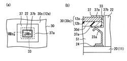
第1実施形態では、導電糸からなる中継部材36の例を示した。これに対し、本実施形態では、金属材料からなる中継部材37を採用し、図6(a),(b)に示すように、中継部材37が、導電性織布12aと非導電性織布12bとに接触して積層織布にかしめ固定されている点を特徴とする。   In the first embodiment, an example of the relay member 36 made of conductive yarn is shown. On the other hand, in this embodiment, the relay member 37 made of a metal material is employed, and the relay member 37 includes the conductive woven fabric 12a and the non-conductive woven fabric, as shown in FIGS. 6 (a) and 6 (b). It is characterized by being caulked and fixed to the laminated woven fabric in contact with 12b.

図6(a),(b)に示す例では、第1成形体30の第2凹部30cに、コネクタ22(貫通孔33)を取り囲むように、複数(6つ)の貫通孔38が形成されている。そして、各貫通孔38に、金属材料からなる中継部材37(例えばリベット様)がそれぞれ挿入されるとともに、貫通孔38から露出する中継部材37の端部が厚さ方向に垂直な方向に延ばされて、第1成形体30にかしめ固定されている。このような中継部材37としては、貫通孔に挿入されて、貫通孔の周辺部位にかしめ固定される周知のものであれば採用することができる。例えば、一端に予め頭部(フランジ部)を有する中継部材37を内面30d側から貫通孔38に挿入し、外面側に露出する他端を潰すことでかしめ固定するようにしても良い。   In the example shown in FIGS. 6A and 6B, a plurality of (six) through holes 38 are formed in the second recess 30c of the first molded body 30 so as to surround the connector 22 (through hole 33). ing. Then, a relay member 37 (for example, a rivet) made of a metal material is inserted into each through hole 38, and the end of the relay member 37 exposed from the through hole 38 extends in a direction perpendicular to the thickness direction. Then, it is caulked and fixed to the first molded body 30. As such a relay member 37, any known member that is inserted into the through hole and caulked and fixed to the peripheral portion of the through hole can be adopted. For example, the relay member 37 having a head (flange portion) at one end in advance may be inserted into the through hole 38 from the inner surface 30d side, and the other end exposed to the outer surface side may be crushed and fixed.

そして、この状態で、基板梱包具12の内面30dをなす非導電性織布12bの表面に、中継部材37の一端部位が位置している。そして、該一端部位に接点ばね23が弾性変形しつつ接触している。なお、図6に示す例では、接点ばね23も、中継部材37に対応して複数(6つ)に分けられている。   In this state, one end portion of the relay member 37 is located on the surface of the non-conductive woven fabric 12 b that forms the inner surface 30 d of the substrate packing tool 12. The contact spring 23 is in contact with the one end portion while being elastically deformed. In the example shown in FIG. 6, the contact spring 23 is also divided into a plurality (six) corresponding to the relay member 37.

このように、積層織布(第1成形体30)にかしめ固定された中継部材37を用いても、第1実施形態に示した導電糸による中継部材36とほぼ同等の効果を奏することができる。   As described above, even when the relay member 37 that is caulked and fixed to the laminated woven fabric (first molded body 30) is used, it is possible to achieve substantially the same effect as the relay member 36 using the conductive yarn shown in the first embodiment. .

なお、第1実施形態の変形例(図5参照)にて示したように、複数の接点ばね23及び中継部材37においては、電磁波シールドの観点から、隣り合う接点ばね23(中継部材37)の間隔を、影響の大きい周波数のうちの最小周波数の1/4以下の間隔とすることが好ましい。図6(a)に示す構成では、隣り合う中継部材37(接点ばね23)の間隔が、影響の大きい周波数のうちの最小周波数の1/4以下となっている。   As shown in the modification of the first embodiment (see FIG. 5), in the plurality of contact springs 23 and relay members 37, from the viewpoint of electromagnetic shielding, the adjacent contact springs 23 (relay members 37) The interval is preferably set to an interval equal to or less than ¼ of the minimum frequency among the frequencies having a large influence. In the configuration shown in FIG. 6A, the interval between the adjacent relay members 37 (contact springs 23) is ¼ or less of the minimum frequency among the frequencies having a great influence.

なお、本実施形態では、電磁波シールド効果を高めるために、貫通孔33を取り囲むべく複数の貫通孔38を第1成形体30に設け、各貫通孔38に中継部材37を配置する例を示した。しかしながら、この構成では、貫通孔38が必要となるため、製造工数が増加し、ひいては製造コストが増加してしまう。また、貫通孔33とは離れた位置に貫通孔38及び中継部材37を設けるため、コネクタ22から接点ばね23が離れてしまい、回路基板11において、接点ばね23も含んで区画された内部空間S1内の電子部品21の実装領域が減少してしまう。さらには、貫通孔33を取り囲もうとすると、第1成形体30における貫通孔33周辺の力学的強度が低下し、第1成形体30が所定形状を維持できなくなる恐れがある。   In the present embodiment, in order to enhance the electromagnetic wave shielding effect, an example in which a plurality of through holes 38 are provided in the first molded body 30 so as to surround the through holes 33 and the relay members 37 are disposed in the respective through holes 38 is shown. . However, in this configuration, since the through hole 38 is necessary, the number of manufacturing steps increases, and the manufacturing cost increases. In addition, since the through hole 38 and the relay member 37 are provided at a position away from the through hole 33, the contact spring 23 is separated from the connector 22, and the internal space S <b> 1 partitioned including the contact spring 23 in the circuit board 11. The mounting area of the electronic component 21 is reduced. Furthermore, if it tries to surround the through-hole 33, the mechanical strength around the through-hole 33 in the first molded body 30 is lowered, and the first molded body 30 may not be able to maintain a predetermined shape.

これに対し、図7(a),(b)に示す例では、第1成形体30の貫通孔33が、図6に示す貫通孔33よりも、コネクタ22に対して大きく設けられ、この貫通孔33に対して、筒状の中継部材37が挿入されるとともに、貫通孔33から露出する中継部材37の端部が厚さ方向に垂直な方向に延ばされて、第1成形体30にかしめ固定されている。そして、この状態で、基板梱包具12の内面30dをなす非導電性織布12bの表面に、中継部材37の一端側のフランジ部37aが位置している。また、中継部材37の筒内部の貫通孔37bが、上記した図6の貫通孔33の機能を果たす。このような構成とすると、上記した課題を解消することができる。さらに、中継部材37を、コネクタ22を取り囲む環状に配置できるので、電磁波シールド効果をより高めることができる。なお、図7は、中継部材の変形例を示す図であり、(a)は平面図、(b)は(a)のVIIb−VIIb線に沿う断面図である。図7は、図6に対応している。   On the other hand, in the example shown in FIGS. 7A and 7B, the through hole 33 of the first molded body 30 is provided larger than the through hole 33 shown in FIG. A cylindrical relay member 37 is inserted into the hole 33, and an end portion of the relay member 37 exposed from the through hole 33 is extended in a direction perpendicular to the thickness direction to form the first molded body 30. It is fixed by caulking. In this state, the flange portion 37 a on one end side of the relay member 37 is located on the surface of the non-conductive woven fabric 12 b that forms the inner surface 30 d of the substrate packing tool 12. Further, the through-hole 37b inside the cylinder of the relay member 37 functions as the above-described through-hole 33 in FIG. With such a configuration, the above-described problems can be solved. Furthermore, since the relay member 37 can be disposed in an annular shape surrounding the connector 22, the electromagnetic wave shielding effect can be further enhanced. FIG. 7 is a view showing a modification of the relay member, in which (a) is a plan view and (b) is a cross-sectional view taken along line VIIb-VIIb in (a). FIG. 7 corresponds to FIG.

なお、本実施形態において、中継部材37以外の構成については、第1実施形態及びその変形例に示した構成を適用することができる。   In addition, in this embodiment, about structures other than the relay member 37, the structure shown in 1st Embodiment and its modification is applicable.

以上、本発明の好ましい実施形態について説明したが、本発明は上記した実施形態になんら制限されることなく、本発明の主旨を逸脱しない範囲において、種々変形して実施することが可能である。   The preferred embodiments of the present invention have been described above. However, the present invention is not limited to the above-described embodiments, and various modifications can be made without departing from the spirit of the present invention.

上記実施形態では、基板梱包具12が、樹脂織布を金属メッキした導電性織布12aと樹脂織布からなる非導電性織布12b(金属メッキなし)との積層織布を成形してなる2つの成形体30,31により構成されており、非導電性織布12bが、基板梱包具12の内面30d,31dをなしている例を示した。しかしながら、基板梱包具12としては、コネクタ22及び接点ばね23が実装された回路基板11の表面11a側を覆う部位として、上記積層織布を含み、積層織布における非導電性織布12bが基板梱包具12の内面30dをなせば良い。   In the said embodiment, the board | substrate packing tool 12 shape | molds the lamination | stacking woven fabric of the electroconductive woven fabric 12a which metal-plated the resin woven fabric, and the nonelectroconductive woven fabric 12b (without metal plating) which consists of a resin woven fabric. An example in which the two molded bodies 30 and 31 are configured and the non-conductive woven fabric 12b forms the inner surfaces 30d and 31d of the substrate packing tool 12 is shown. However, as the substrate packing tool 12, the above-mentioned laminated woven fabric is included as a portion covering the surface 11a side of the circuit board 11 on which the connector 22 and the contact spring 23 are mounted, and the non-conductive woven fabric 12b in the laminated woven fabric is the substrate. The inner surface 30d of the packing tool 12 may be formed.

例えば図8に示すように、基板梱包具12が、回路基板11の表面11a側を覆う部位130(以下、単に表面部位130と示す)と、回路基板11の裏面11b側を覆う部位131(以下、単に裏面部位131と示す)とが一体的に成形された1つの成形体からなる構成としても良い。この基板梱包具12でも、成形体は、導電性織布12aと非導電性織布12bとの積層織布を成形してなり、非導電性織布12bが、基板梱包具12の内面130d,131dをなしている。なお、表面部位130は上記した第1成形体30、裏面部位131は上記した第2成形体31とほぼ同じ構造となっており、図8では、対応する箇所において、2つの成形体30,31の符号に100を加算した符号を付与している。表面部位130と裏面部位131とは、連結部位138を介して連結されている。詳しくは、平面矩形状の表面部位130及び裏面部位131のうち、矩形の1辺のみが連結部位138により連結されている。この連結部位138には、切り欠き138aが設けられており、これにより、内部空間S1を形成すべく折曲可能となっている。すなわち、基板梱包具12は、所謂卵パック様の構造となっている。このような構成の電子装置10としても、上記実施形態に示した電子装置10と同様の効果を期待することができる。また、成形体が所謂卵パック様となっているので、成形体から基板梱包具12を形成する工程を簡素化することができる。なお、図8では、中継部材136として、導電糸からなる例を示しているが、かしめ固定されるものを適用することもできる。図8は、基板梱包具のその他変形例を示す断面図であり、上記した図3に対応している。   For example, as shown in FIG. 8, the substrate packing tool 12 covers a portion 130 (hereinafter simply referred to as a surface portion 130) that covers the front surface 11 a side of the circuit board 11 and a portion 131 (hereinafter referred to as the back surface 11 b side) of the circuit board 11. The back surface portion 131 may be formed as a single body. Also in this substrate packaging tool 12, the molded body is formed by forming a laminated woven fabric of a conductive woven fabric 12a and a non-conductive woven fabric 12b, and the non-conductive woven fabric 12b is formed on the inner surface 130d, 131d. The front surface portion 130 has substantially the same structure as the above-described first molded body 30 and the back surface portion 131 has the same structure as the above-described second molded body 31. In FIG. The code | symbol which added 100 to the code | symbol of is given. The front surface part 130 and the back surface part 131 are connected via a connection part 138. Specifically, only one side of the rectangular shape of the front surface portion 130 and the back surface portion 131 having a planar rectangular shape is connected by the connection portion 138. The connection portion 138 is provided with a notch 138a, which can be bent to form the internal space S1. That is, the substrate packing tool 12 has a so-called egg pack-like structure. The electronic device 10 having such a configuration can be expected to have the same effect as the electronic device 10 described in the above embodiment. Moreover, since the molded body has a so-called egg pack shape, the process of forming the substrate packing tool 12 from the molded body can be simplified. In addition, in FIG. 8, although the example which consists of a conductive thread | yarn is shown as the relay member 136, the thing fixed by crimping is also applicable. FIG. 8 is a cross-sectional view showing another modification of the substrate packing tool, and corresponds to FIG. 3 described above.

また、図9に示すように、基板梱包具12が、回路基板11の表面11a側を覆う部位として、第1実施形態で示した第1成形体30とほぼ同じ構造の成形体230を有し、回路基板11の裏面11b側を覆う部位として金属材料からなる平板状の金属板231を有する構成としても良い。この基板梱包具12でも、成形体230は、導電性織布12aと非導電性織布12bとの積層織布を成形してなり、非導電性織布12bが、基板梱包具12の内面230dをなしている。図9では、対応する箇所において、2つの成形体30,31の符号に200を加算した符号を付与している。図9に示す回路基板11は、表面11a側のみに電子部品21が実装されている。また、第2ケース41の第1凹部41bが、第2凹部41cとフラットな構成、すなわち、第2ケース41が縁部41aを基準として2段の凹構造となっている。さらには、成形体230の縁部230aと金属板231の縁部231aに、金属部材235がかしめ固定され、これにより、成形体230をなす導電性織布12aと金属板231とが、電気的に接続されている。この金属部材235は、基板梱包具12が、電磁波シールド効果を発揮すべく、影響の大きい周波数のうちの最小周波数の1/4以下の間隔をもって複数個所に固定されている。このような構成の電子装置10としても、上記実施形態に示した電子装置10と同様の効果を期待することができる。なお、導電性織布12aと非導電性織布12bとの積層織布を成形してなる成形体230と金属板231により、基板梱包具12が構成されており、基板梱包具12として、主材料が樹脂織布である成形体230を含むので、基板梱包具12全てが積層織布からなる電子装置10よりは重くなるものの、従来の金属筐体に比べて、電子装置10を軽量化することができる。図9も、基板梱包具のその他変形例を示す断面図であり、上記した図3に対応している。   Moreover, as shown in FIG. 9, the board | substrate packing tool 12 has the molded object 230 of the structure substantially the same as the 1st molded object 30 shown in 1st Embodiment as a site | part which covers the surface 11a side of the circuit board 11. As shown in FIG. A configuration may be adopted in which a flat metal plate 231 made of a metal material is provided as a portion covering the back surface 11b side of the circuit board 11. Also in this substrate packaging tool 12, the molded body 230 is formed by molding a laminated woven fabric of the conductive woven fabric 12a and the non-conductive woven fabric 12b, and the non-conductive woven fabric 12b is formed on the inner surface 230d of the substrate packaging device 12. I am doing. In FIG. 9, the code | symbol which added 200 to the code | symbol of the two molded objects 30 and 31 is provided in the corresponding location. As for the circuit board 11 shown in FIG. 9, the electronic component 21 is mounted only in the surface 11a side. In addition, the first recess 41b of the second case 41 is flat with the second recess 41c, that is, the second case 41 has a two-stage recess structure with the edge 41a as a reference. Further, the metal member 235 is caulked and fixed to the edge portion 230a of the molded body 230 and the edge portion 231a of the metal plate 231. As a result, the conductive woven fabric 12a and the metal plate 231 forming the molded body 230 are electrically connected. It is connected to the. The metal member 235 is fixed at a plurality of positions with an interval equal to or less than ¼ of the minimum frequency among the frequencies having a large influence so that the substrate packing tool 12 exhibits an electromagnetic wave shielding effect. The electronic device 10 having such a configuration can be expected to have the same effect as the electronic device 10 described in the above embodiment. The substrate packing tool 12 is composed of a molded body 230 formed by molding a laminated woven fabric of the conductive woven fabric 12a and the non-conductive woven fabric 12b and the metal plate 231. Since the material includes the molded body 230 made of a resin woven fabric, the entire substrate packing tool 12 is heavier than the electronic device 10 made of a laminated woven fabric, but the weight of the electronic device 10 is reduced compared to a conventional metal casing. be able to. FIG. 9 is also a cross-sectional view showing another modification of the substrate packing tool, and corresponds to FIG. 3 described above.

さらには、図示しないが、基板梱包具12の構成する積層織布として、未成形のものを採用することもできる。例えば、図3に示す2つの成形体30,31に代えて、未成形の積層織布を採用しても良いし、図9に示す成形体230に代えて、未成形の積層織布を採用しても良い。このように未成形の積層織布を用いた基板梱包具12を採用すると、成形工程を省略できるので、製造工程を簡素化し、製造コストを低減することができる。しかしながら、回路基板11が基板梱包具12と接触するので、電子部品21の接続信頼性の低下などが懸念される。また、接点ばね23との接触を確保すべく、成形体に比べて、中継部材36を広範囲に固定しなければならなくなる。   Furthermore, although not shown in figure, as the laminated woven fabric which the board | substrate packing tool 12 comprises, an unshaped thing can also be employ | adopted. For example, an unmolded laminated woven fabric may be adopted instead of the two molded bodies 30, 31 shown in FIG. 3, or an unmolded laminated woven fabric is adopted instead of the molded body 230 shown in FIG. You may do it. Thus, when the board | substrate packing tool 12 using a non-molded laminated woven fabric is employ | adopted, since a formation process can be skipped, a manufacturing process can be simplified and manufacturing cost can be reduced. However, since the circuit board 11 comes into contact with the board packaging tool 12, there is a concern that the connection reliability of the electronic component 21 is lowered. Further, in order to ensure contact with the contact spring 23, it is necessary to fix the relay member 36 in a wider range than the molded body.

上記実施形態では、電子装置10が、回路基板11及び基板梱包具12を保護する筐体13を含む例を示した。しかしながら、電子装置10として筐体13を含まず、基板梱包具12が筐体を兼ねる構成としても良い。この場合、上記した2つの成形体30,31からなる基板梱包具12、表面部位130と裏面部位131を備えた1つの成形体からなる基板梱包具12、及び成形体230及び金属板231からなる基板梱包具12のいずれかを採用すると、回路基板11を外部から好適に保護することができる。   In the said embodiment, the electronic device 10 showed the example containing the housing | casing 13 which protects the circuit board 11 and the board | substrate packing tool 12. As shown in FIG. However, the electronic device 10 may not include the housing 13 and the substrate packing tool 12 may also serve as the housing. In this case, the substrate packing tool 12 including the two molded bodies 30 and 31 described above, the substrate packing tool 12 including one molded body having the front surface portion 130 and the back surface portion 131, and the molded body 230 and the metal plate 231 are included. When any one of the board packing tools 12 is employed, the circuit board 11 can be suitably protected from the outside.

上記実施形態では、螺子50により、回路基板11を基板梱包具12に固定するとともに、回路基板11及び基板梱包具12を筐体13(第2ケース41)に固定する例を示した。しかしながら、回路基板11を基板梱包具12に固定する固定手段と、回路基板11及び基板梱包具12を筐体13(第2ケース41)に固定する固定手段とを別個のものとしても良い。例えば図10に示す例では、螺子50による固定箇所も、上記した螺子52による回路基板11を基板梱包具12に固定する箇所に置き換えられている。すなわち、図10では、8箇所で、回路基板11が基板梱包具12に螺子52により固定されている。また、導電糸35により縁部30a,31aが縫い合わされ、縁部30a,31a全周に亘って、導電性織布12a同士が電気的に接続された基板梱包具12は、内部空間S1に回路基板11を収容した状態で、縁部30a,31aが、第1ケース40の縁部40aにおける内周部位と第2ケース41における第1凹部41bとの間で挟持されている。これにより、回路基板11及び基板梱包具12が筐体13に固定されている。なお、第1ケース40の縁部40aは、第2ケース41の縁部41aと対向する外周部位とともに、上記した内周部位を有している。図10は、電子装置のその他変形例を示す断面図であり、上記した図3に対応している。   In the embodiment described above, the example in which the circuit board 11 is fixed to the board packaging tool 12 by the screw 50 and the circuit board 11 and the board packaging tool 12 are fixed to the housing 13 (second case 41) has been described. However, the fixing means for fixing the circuit board 11 to the board packing tool 12 and the fixing means for fixing the circuit board 11 and the board packing tool 12 to the housing 13 (second case 41) may be separate. For example, in the example shown in FIG. 10, the fixing portion by the screw 50 is also replaced with the portion for fixing the circuit board 11 by the screw 52 to the substrate packing tool 12. That is, in FIG. 10, the circuit board 11 is fixed to the board packing tool 12 by screws 52 at eight places. Also, the board packaging 12 in which the edges 30a and 31a are stitched together by the conductive yarn 35 and the conductive woven fabrics 12a are electrically connected over the entire circumference of the edges 30a and 31a is connected to the internal space S1. In a state where the substrate 11 is accommodated, the edge portions 30 a and 31 a are sandwiched between the inner peripheral portion of the edge portion 40 a of the first case 40 and the first recess portion 41 b of the second case 41. As a result, the circuit board 11 and the board packing tool 12 are fixed to the housing 13. In addition, the edge part 40a of the 1st case 40 has the above-mentioned inner peripheral part with the outer peripheral part facing the edge part 41a of the 2nd case 41. As shown in FIG. FIG. 10 is a cross-sectional view showing another modification of the electronic device, and corresponds to FIG. 3 described above.

また、回路基板11と第1成形体30を固定する螺子と、回路基板11と第2成形体31を固定する螺子を分けても良い。さらには、第2成形体31を第2ケース41に固定する螺子、回路基板11を第2ケース41に固定する螺子、第1成形体30を第2ケース41に固定する螺子を分けても良い。   Further, a screw for fixing the circuit board 11 and the first molded body 30 and a screw for fixing the circuit board 11 and the second molded body 31 may be separated. Furthermore, a screw for fixing the second molded body 31 to the second case 41, a screw for fixing the circuit board 11 to the second case 41, and a screw for fixing the first molded body 30 to the second case 41 may be divided. .

上記実施形態では、筐体13が、2つのケース40,41からなる例を示した。しかしながら、図8で示した基板梱包具12のように、回路基板11の表面11a側を覆う部位(表面部位)と、回路基板11の裏面11b側を覆う部位(裏面部位)とを有し、表面部位と裏面部位とが連結部位を介して連結された所謂卵パック様の構造としても良い。このように、卵パック様の構造としても、図3に示す螺子50による基板梱包具12の筐体13(第2ケース41)への固定、図10に例示した挟持による基板梱包具12の固定のいずれも適用することができる。   In the above-described embodiment, the case 13 includes the two cases 40 and 41. However, like the substrate packing tool 12 shown in FIG. 8, it has a portion (front surface portion) covering the front surface 11 a side of the circuit board 11 and a portion (back surface portion) covering the back surface 11 b side of the circuit board 11, A so-called egg pack-like structure in which the front surface portion and the back surface portion are connected via a connecting portion may be used. In this way, even in an egg pack-like structure, the board packing tool 12 is fixed to the housing 13 (second case 41) by the screw 50 shown in FIG. 3, and the board packing tool 12 is fixed by clamping illustrated in FIG. Any of these can be applied.

上記実施形態では、筐体13が、厚さ方向に開閉可能に構成されている例を示した。しかしながら、筐体13により、基板梱包具12を挟持する構成でない場合、筐体13の構成は上記例に限定されるものではない。例えば、厚さ方向に垂直な方向に開閉可能に構成された筐体13を採用することもできる。   In the above embodiment, an example in which the housing 13 is configured to be openable and closable in the thickness direction has been described. However, the configuration of the housing 13 is not limited to the above example when the substrate packaging tool 12 is not sandwiched by the housing 13. For example, the housing 13 configured to be openable and closable in a direction perpendicular to the thickness direction can be employed.

上記実施形態では、導電性織布12aと非導電性織布12bとの間に接着剤を介在させて積層織布が構成される例を示した。しかしながら、導電性織布12aと非導電性織布12bとを一体化される手法は上記例に限定されるものではない。例えば、非導電性織布12bを構成する樹脂として、導電性織布12aを構成する樹脂よりも融点の低い熱可塑性樹脂を採用し、圧空成形などの成形時に、熱を受けて軟化した非導電性織布12bを導電性織布12aに密着させて積層織布としたものでも良い。   In the above embodiment, an example in which a laminated woven fabric is configured by interposing an adhesive between the conductive woven fabric 12a and the non-conductive woven fabric 12b has been described. However, the method for integrating the conductive woven fabric 12a and the non-conductive woven fabric 12b is not limited to the above example. For example, as the resin constituting the non-conductive woven fabric 12b, a thermoplastic resin having a melting point lower than that of the resin constituting the conductive woven fabric 12a is adopted, and the non-conductive is softened by receiving heat during molding such as pressure forming. The laminated woven fabric may be formed by bringing the conductive woven fabric 12b into close contact with the conductive woven fabric 12a.

また、回路基板11、基板梱包具12、筐体13の構造は、上記例に限定されるものではない。例えば、第1実施形態や第2実施形態において、第2ケース41の第1凹部41bが、第2凹部41cとフラットな構成、すなわち、縁部41aを基準として2段の凹構造としても良い。   Moreover, the structure of the circuit board 11, the board | substrate packing tool 12, and the housing | casing 13 is not limited to the said example. For example, in 1st Embodiment or 2nd Embodiment, the 1st recessed part 41b of the 2nd case 41 is good also as a 2 step | paragraph recessed structure on the basis of the 2nd recessed part 41c, ie, the edge 41a.

10・・・電子装置
11・・・回路基板
12・・・基板梱包具
12a・・・導電性織布
12b・・・非導電性織布
13・・・筐体
22・・・コネクタ
23・・・接点ばね
30・・・第1成形体
31・・・第2成形体
36,37・・・中継部材
S1・・・内部空間
DESCRIPTION OF SYMBOLS 10 ... Electronic device 11 ... Circuit board 12 ... Board packing tool 12a ... Conductive woven cloth 12b ... Non-conductive woven cloth 13 ... Housing 22 ... Connector 23 ... Contact spring 30: first molded body 31: second molded body 36, 37: relay member S1: internal space

Claims (8)

第1主面及び該第1主面の裏面である第2主面の少なくとも一方に電子部品が実装された回路基板と、
前記回路基板を内部空間に収容し、前記回路基板の電磁波シールドを行う基板梱包具と、
金属材料からなり、前記回路基板における第1主面に実装されて、前記回路基板のGNDパターンと前記基板梱包具とを電気的に接続する接点ばねと、を備える電子装置であって、
前記基板梱包具は、樹脂織布を金属メッキした導電性織布と樹脂織布からなる非導電性織布との積層織布を、少なくとも前記回路基板の第1主面側を覆う部位として含むとともに、前記非導電性織布が前記基板梱包具の内面をなしており、
前記積層織布には導電性の中継部材が固定され、該中継部材は、前記導電性織布と電気的に接続されるとともに、前記基板梱包具の内面をなす前記非導電性織布の表面において前記接点ばねの接触部位に配置されていることを特徴とする電子装置。
A circuit board on which electronic components are mounted on at least one of the first main surface and the second main surface which is the back surface of the first main surface;
A circuit board packing tool for accommodating the circuit board in an internal space and performing electromagnetic wave shielding of the circuit board;
An electronic device comprising a contact spring made of a metal material, mounted on a first main surface of the circuit board, and electrically connecting the GND pattern of the circuit board and the board packaging tool,
The substrate packing tool includes a laminated woven fabric of a conductive woven fabric obtained by metal plating a resin woven fabric and a non-conductive woven fabric made of a resin woven fabric as a portion covering at least the first main surface side of the circuit board. And the non-conductive woven fabric forms the inner surface of the substrate packing tool,
A conductive relay member is fixed to the laminated woven fabric, and the relay member is electrically connected to the conductive woven fabric, and the surface of the non-conductive woven fabric forming the inner surface of the substrate packing tool. The electronic device according to claim 1, wherein the electronic device is disposed at a contact portion of the contact spring.
前記中継部材は、導電性を有する導電糸であり、
前記導電糸により、前記導電性織布と前記非導電性織布とが縫われていることを特徴とする請求項1に記載の電子装置。
The relay member is a conductive yarn having conductivity,
The electronic device according to claim 1, wherein the conductive woven fabric and the non-conductive woven fabric are sewn by the conductive yarn.
前記中継部材は、金属材料からなり、前記導電性織布と前記非導電性織布とに接触して前記積層織布にかしめ固定されていることを特徴とする請求項1に記載の電子装置。   2. The electronic device according to claim 1, wherein the relay member is made of a metal material and is caulked and fixed to the laminated woven fabric in contact with the conductive woven fabric and the non-conductive woven fabric. . 前記接点ばねは、前記回路基板に実装されたコネクタのシールドとして、前記コネクタの周辺に設けられていることを特徴とする請求項1〜3いずれか1項に記載の電子装置。   The electronic device according to claim 1, wherein the contact spring is provided around the connector as a shield of the connector mounted on the circuit board. 前記基板梱包具は、前記積層織布の成形体としての、前記回路基板の第1主面側を覆う第1成形体、及び、前記回路基板の第2主面側を覆う第2成形体からなることを特徴とする請求項1〜4いずれか1項に記載の電子装置。   The board packing tool includes a first molded body covering the first main surface side of the circuit board as a molded body of the laminated woven fabric, and a second molded body covering the second main surface side of the circuit board. The electronic device according to claim 1, wherein the electronic device is an electronic device. 前記基板梱包具は、前記積層織布の成形体からなり、前記回路基板の第1主面側を覆う部位と、前記回路基板の第2主面側を覆う部位とが一体成形されていることを特徴とする請求項1〜4いずれか1項に記載の電子装置。   The board packing tool is made of a molded body of the laminated woven fabric, and a part covering the first main surface side of the circuit board and a part covering the second main surface side of the circuit board are integrally formed. The electronic device according to claim 1, wherein: 前記基板梱包具は、前記回路基板の第1主面側を覆う部位として、前記積層織布の成形体を有するともに、前記回路基板の第2主面側を覆う部位として、金属板を有することを特徴とする請求項1〜4いずれか1項に記載の電子装置。   The board packaging tool has a molded body of the laminated woven fabric as a part covering the first main surface side of the circuit board and a metal plate as a part covering the second main surface side of the circuit board. The electronic device according to claim 1, wherein: 前記成形体が、圧空成形により形成されてなることを特徴とする請求項5〜7いずれか1項に記載の電子装置。   The electronic device according to claim 5, wherein the molded body is formed by pressure forming.
JP2009120267A 2009-05-18 2009-05-18 Electronic equipment Expired - Fee Related JP5115518B2 (en)

Priority Applications (1)

Application Number Priority Date Filing Date Title
JP2009120267A JP5115518B2 (en) 2009-05-18 2009-05-18 Electronic equipment

Applications Claiming Priority (1)

Application Number Priority Date Filing Date Title
JP2009120267A JP5115518B2 (en) 2009-05-18 2009-05-18 Electronic equipment

Publications (2)

Publication Number Publication Date
JP2010267928A JP2010267928A (en) 2010-11-25
JP5115518B2 true JP5115518B2 (en) 2013-01-09

Family

ID=43364631

Family Applications (1)

Application Number Title Priority Date Filing Date
JP2009120267A Expired - Fee Related JP5115518B2 (en) 2009-05-18 2009-05-18 Electronic equipment

Country Status (1)

Country Link
JP (1) JP5115518B2 (en)

Families Citing this family (3)

* Cited by examiner, † Cited by third party
Publication number Priority date Publication date Assignee Title
JP5873996B2 (en) * 2011-02-18 2016-03-01 パナソニックIpマネジメント株式会社 Optical disk drive and wiring structure
JP6222752B2 (en) * 2016-02-09 2017-11-01 Necプラットフォームズ株式会社 Conductive sheet mounting structure and electronic device
DE102020202965A1 (en) 2020-03-09 2021-09-09 Volkswagen Aktiengesellschaft Battery housing with at least two interconnected housing elements and a method for producing a connection of at least two housing elements to form a battery housing

Family Cites Families (5)

* Cited by examiner, † Cited by third party
Publication number Priority date Publication date Assignee Title
JPS58182496U (en) * 1982-05-31 1983-12-05 日野自動車株式会社 Radio interference prevention device for electronic devices
JP2674945B2 (en) * 1993-12-20 1997-11-12 株式会社トキメック Electromagnetic shielding material and electromagnetic shielding space construct using the same
JPH08130387A (en) * 1994-11-02 1996-05-21 Fujitsu Ltd Shield structure of circuit unit
JP2007227767A (en) * 2006-02-24 2007-09-06 Optrex Corp Electromagnetic shield structure of electronics
JP5332164B2 (en) * 2006-10-13 2013-11-06 東レ株式会社 Method for suppressing noise from electronic devices

Also Published As

Publication number Publication date
JP2010267928A (en) 2010-11-25

Similar Documents

Publication Publication Date Title
CN107112736B (en) Electronic control unit
US7639513B2 (en) Radio frequency module and manufacturing method thereof
JP4234259B2 (en) Combination structure of electronic equipment
US8773867B2 (en) Camera module for shielding EMI
JP5169696B2 (en) Sealing device and sealing structure
US9345134B2 (en) Printed wiring board
JP5287492B2 (en) Electronic equipment
JP6542642B2 (en) Electronic control unit
JP2014093792A (en) On-vehicle electronic control unit
US20060046533A1 (en) Substrate for connector
JP2010509742A (en) Standardized electronic casing with modular contact partner
CN214256936U (en) Module
JP5417984B2 (en) Electronic equipment
WO2008059643A1 (en) Three-dimensional electronic circuit apparatus
JP5115518B2 (en) Electronic equipment
US20080066953A1 (en) Circuit board assembly and manufacturing method thereof, electronic part assembly and manufacturing method thereof, and electronic device
EP2892309A1 (en) Electric device for electric vehicle
JP2009272499A (en) Electronic control unit
US7269032B2 (en) Shielding for EMI-sensitive electronic components and or circuits of electronic devices
WO2017094834A1 (en) Electronic component module equipped with heat sink and substrate having electronic components mounted thereon, and method for producing same
US20140334109A1 (en) Electronic Component Module and Method of Manufacturing the Same
JP2019096646A (en) Electronic equipment
JP4928281B2 (en) Electromagnetic shielding member
JP2010092740A (en) Board-cable connection structure
CN111913144B (en) Housing structure for a magnetic resonance system, electronic component and magnetic resonance system

Legal Events

Date Code Title Description
A621 Written request for application examination

Free format text: JAPANESE INTERMEDIATE CODE: A621

Effective date: 20110627

A977 Report on retrieval

Free format text: JAPANESE INTERMEDIATE CODE: A971007

Effective date: 20120912

TRDD Decision of grant or rejection written
A01 Written decision to grant a patent or to grant a registration (utility model)

Free format text: JAPANESE INTERMEDIATE CODE: A01

Effective date: 20120918

A01 Written decision to grant a patent or to grant a registration (utility model)

Free format text: JAPANESE INTERMEDIATE CODE: A01

A61 First payment of annual fees (during grant procedure)

Free format text: JAPANESE INTERMEDIATE CODE: A61

Effective date: 20121001

FPAY Renewal fee payment (event date is renewal date of database)

Free format text: PAYMENT UNTIL: 20151026

Year of fee payment: 3

R250 Receipt of annual fees

Free format text: JAPANESE INTERMEDIATE CODE: R250

R250 Receipt of annual fees

Free format text: JAPANESE INTERMEDIATE CODE: R250

LAPS Cancellation because of no payment of annual fees