JP5115217B2 - Dot matrix type liquid crystal display device - Google Patents
Dot matrix type liquid crystal display device Download PDFInfo
- Publication number
- JP5115217B2 JP5115217B2 JP2008019021A JP2008019021A JP5115217B2 JP 5115217 B2 JP5115217 B2 JP 5115217B2 JP 2008019021 A JP2008019021 A JP 2008019021A JP 2008019021 A JP2008019021 A JP 2008019021A JP 5115217 B2 JP5115217 B2 JP 5115217B2
- Authority
- JP
- Japan
- Prior art keywords
- polarity
- liquid crystal
- voltage
- scan lines
- reset
- Prior art date
- Legal status (The legal status is an assumption and is not a legal conclusion. Google has not performed a legal analysis and makes no representation as to the accuracy of the status listed.)
- Active
Links
Images


Description
本発明は、ドットマトリクス型液晶表示装置に関し、特にコレステリック液晶を使用し、表示データの書込み前に第1ステップでプレーナ状態またはフォーカルコニック状態にリセットするリセット動作を行うドットマトリクス型液晶表示装置に関する。 The present invention relates to a dot matrix type liquid crystal display device, and more particularly to a dot matrix type liquid crystal display device using a cholesteric liquid crystal and performing a reset operation to reset to a planar state or a focal conic state in a first step before writing display data.
液晶表示素子のようなドットマトリクス型表示素子が、テレビ受像機やコンピュータシステムのモニタとして広く使用されている。ドットマトリクス型表示素子は、平行に配列された複数のスキャンラインと、スキャンラインと垂直に交差するように配置された複数のデータライン(セグメントライン)とを有し、複数のスキャンラインと複数のセグメントラインの交差部に画素が形成される。表示する画像の書込みは、スキャンラインに順次スキャンパルスを印加し、スキャンパルスの印加に同期して複数のセグメントラインに1ライン分のデータを出力することにより行われる。ドットマトリクス型表示素子には、CRT、PDP、EL、液晶表示素子など各種の方式があるが、特に液晶表示素子が広く使用されている。 A dot matrix type display element such as a liquid crystal display element is widely used as a monitor of a television receiver or a computer system. The dot matrix display device has a plurality of scan lines arranged in parallel and a plurality of data lines (segment lines) arranged so as to intersect the scan lines perpendicularly. Pixels are formed at the intersections of the segment lines. Writing of an image to be displayed is performed by sequentially applying scan pulses to the scan lines and outputting data for one line to a plurality of segment lines in synchronization with the application of the scan pulses. There are various types of dot matrix type display elements such as CRT, PDP, EL, and liquid crystal display elements, and liquid crystal display elements are particularly widely used.
近年、電源を切っても表示内容を保持できる書換え可能な表示デバイスとして、各企業および大学などにおいて、電子ペーパーの開発が盛んに進められている。電子ペーパーの利用が期待されている応用分野として、電子書籍を筆頭に、モバイル端末機器のサブディスプレイやICカードの表示部など、多様な応用形態が提案されている。電子ペーパーの有力な方式の1つに、コレステリック液晶がある。コレステリック液晶は、半永久的な表示保持(メモリ性)や鮮やかなカラー表示、高コントラスト、高解像度といった優れた特徴を有している。 In recent years, electronic paper has been actively developed at companies and universities as rewritable display devices that can retain display contents even when the power is turned off. As application fields in which electronic paper is expected to be used, various application forms such as electronic books, sub-displays for mobile terminal devices, and display units for IC cards have been proposed. One of the leading methods for electronic paper is cholesteric liquid crystal. Cholesteric liquid crystal has excellent characteristics such as semi-permanent display retention (memory property), vivid color display, high contrast, and high resolution.
コレステリック液晶は、カライラルネマティック液晶とも称されることがあり、ネマティック液晶にキラル性の添加剤(カイラル材)を比較的多く(数十%)添加することにより、ネマティック液晶の分子がらせん状のコレステリック相を形成する液晶である。 Cholesteric liquid crystals are sometimes referred to as chiral nematic liquid crystals, and by adding a relatively large amount (several tens of percent) of chiral additives (chiral materials) to nematic liquid crystals, the molecules of nematic liquid crystals are helical. It is a liquid crystal that forms a cholesteric phase.
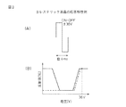
図1は、コレステリック液晶の状態を説明する図である。図1の(A)および(B)に示すように、コレステリック液晶を利用した表示素子10は、上側基板11と、コレステリック液晶層12と、下側基板13と、有する。コレステリック液晶には、図1の(A)に示すように入射光を反射するプレーナ状態と、図1の(B)に示すように入射光を透過するフォーカルコニック状態と、があり、これらの状態は、無電界下でも安定してその状態が保持される。
FIG. 1 is a diagram for explaining a state of a cholesteric liquid crystal. As shown in FIGS. 1A and 1B, the
プレーナ状態の時には、液晶分子のらせんピッチに応じた波長の光を反射する。反射が最大となる波長λは、液晶の平均屈折率n、らせんピッチpから次の式で表される。 In the planar state, light having a wavelength corresponding to the helical pitch of the liquid crystal molecules is reflected. The wavelength λ at which the reflection is maximum is expressed by the following formula from the average refractive index n of the liquid crystal and the helical pitch p.
λ=n・p
一方、反射帯域Δλは、液晶の屈折率異方性Δnにより大きく異なる。
λ = n · p
On the other hand, the reflection band Δλ varies greatly depending on the refractive index anisotropy Δn of the liquid crystal.
プレーナ状態の時には、入射光が反射するので「明」状態、すなわち白を表示することができる。一方、フォーカルコニック状態の時には、下側基板13の下に光吸収層を設けることにより、液晶層を透過した光が吸収されるので「暗」状態、すなわち黒を表示することができる。
In the planar state, incident light is reflected, so that a “bright” state, that is, white can be displayed. On the other hand, in the focal conic state, by providing a light absorption layer under the
上記のように、プレーナ状態の時には、液晶分子のらせんピッチに応じた波長の光を反射するので、液晶材料およびカイラル材を選択し、カイラル材の含有率を決定し、青(ブルー)、緑(グリーン)および赤(レッド)の各波長を選択反射する3つのパネルを得、それらを積層して、カラー表示素子が得られる。 As described above, in the planar state, light of a wavelength corresponding to the helical pitch of the liquid crystal molecules is reflected. Therefore, the liquid crystal material and the chiral material are selected, the content of the chiral material is determined, and blue (blue), green Three panels that selectively reflect each wavelength of (green) and red (red) are obtained, and they are laminated to obtain a color display element.
次に、コレステリック液晶を利用した表示素子の駆動方法を説明する。 Next, a method for driving a display element using cholesteric liquid crystal will be described.
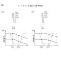
図2は、一般的なコレステリック液晶の電圧−反射特性の一例を示している。横軸は、コレステリック液晶を挟む電極間に所定のパルス幅で印加されるパルス電圧の電圧値(V)を表し、縦軸はコレステリック液晶の反射率(%)を表している。図2に示す実線の曲線Pは、初期状態がプレーナ状態のコレステリック液晶の電圧−反射率特性を示し、破線の曲線FCは、初期状態がフォーカルコニック状態のコレステリック液晶の電圧−反射率特性を示す。 FIG. 2 shows an example of voltage-reflection characteristics of a general cholesteric liquid crystal. The horizontal axis represents the voltage value (V) of the pulse voltage applied with a predetermined pulse width between the electrodes sandwiching the cholesteric liquid crystal, and the vertical axis represents the reflectance (%) of the cholesteric liquid crystal. The solid curve P shown in FIG. 2 shows the voltage-reflectance characteristics of the cholesteric liquid crystal whose initial state is the planar state, and the broken curve FC shows the voltage-reflectance characteristics of the cholesteric liquid crystal whose initial state is the focal conic state. .
図2において、電極間に所定の高電圧VP100(例えば±36V)を印加して、コレステリック液晶中に相対的に強い電界を発生させると、液晶分子のらせん構造は完全にほどけて、すべての分子が電界の方向に従うホメオトロピック状態になる。次に、液晶分子がホメオトロピック状態の時に、印加電圧をVP100から所定の低電圧(例えば、VF0=±4V)に急激に低下させて、液晶中の電界を急激にほぼゼロにすると、液晶のらせん軸は電極に垂直になり、らせんピッチに応じた光を選択的に反射するプレーナ状態になる。 In FIG. 2, when a predetermined high voltage VP100 (for example, ± 36 V) is applied between the electrodes to generate a relatively strong electric field in the cholesteric liquid crystal, the helical structure of the liquid crystal molecules is completely unwound and all molecules are Becomes homeotropic according to the direction of the electric field. Next, when the liquid crystal molecules are in a homeotropic state, the applied voltage is rapidly decreased from VP100 to a predetermined low voltage (for example, VF0 = ± 4 V), and the electric field in the liquid crystal is suddenly reduced to almost zero. The spiral axis is perpendicular to the electrode, and a planar state in which light according to the spiral pitch is selectively reflected is obtained.
一方、電極間に所定の低電圧VF100b(例えば、±24V)を印加し、コレステリック液晶中の相対的に弱い電界を発生させると、液晶分子のらせん構造が完全には解けない状態になる。この状態において、印加電圧をVF100bから低電圧VF0に急激に低下させて、液晶中の電界を急激にほぼゼロにするか、あるいは強い電界を印加し緩やかに電界を除去した場合は、液晶分子のらせん軸が電極に平行になり、入射光を透過するフォーカルコニック状態になる。 On the other hand, when a predetermined low voltage VF100b (for example, ± 24V) is applied between the electrodes to generate a relatively weak electric field in the cholesteric liquid crystal, the spiral structure of the liquid crystal molecules cannot be completely solved. In this state, when the applied voltage is suddenly lowered from VF100b to the low voltage VF0 and the electric field in the liquid crystal is suddenly made substantially zero, or a strong electric field is applied and the electric field is gently removed, The helical axis is parallel to the electrode, and a focal conic state in which incident light is transmitted is obtained.
また、中間的な強さの電界を印加し、急激に電界を除去すると、プレーナ状態とフォーカルコニック状態が混在し、中間調の表示が可能となる。 In addition, when an electric field having an intermediate strength is applied and the electric field is rapidly removed, a planar state and a focal conic state are mixed, and halftone display is possible.
ここで、図2に示す曲線Pにおいて、破線枠A内では、印加する電圧パルスの電圧値を高くするに従ってフォーカルコニック状態の割合を増加させてコレステリック液晶の反射率を低下させることができる。また、図2に示す曲線PおよびFCにおいて、破線枠B内では、印加する電圧値を低くするに従ってフォーカルコニック状態の割合を増加させてコレステリック液晶の反射率を低下させることができる。 Here, in the curve P shown in FIG. 2, within the broken line frame A, the reflectance of the cholesteric liquid crystal can be lowered by increasing the ratio of the focal conic state as the voltage value of the applied voltage pulse is increased. Further, in the curves P and FC shown in FIG. 2, within the broken line frame B, the reflectance of the cholesteric liquid crystal can be lowered by increasing the ratio of the focal conic state as the applied voltage value is lowered.
中間調を表示するためには、A領域またはB領域を利用する。A領域を利用する場合には、画素を初期化してプレーナ状態にした後に、VF0とVF100aの間の電圧パルスを印加して一部をフォーカルコニック状態にする。また、B領域を利用する場合には、画素を初期化してフォーカルコニック状態にした後に、VF100bとVP0の間の電圧パルスを印加して一部をプレーナ状態にする。 In order to display a halftone, area A or area B is used. When the area A is used, after a pixel is initialized and brought into a planar state, a voltage pulse between VF0 and VF100a is applied to partially bring the focal conic state. Further, when the region B is used, a pixel is initialized to a focal conic state, and then a voltage pulse between VF100b and VP0 is applied to partially make a planar state.
以上説明した電圧応答特性に基づく駆動方法の原理を、図3および図4を参照して説明する。図3の(A)、図4の(A)および(C)は電圧パルスの波形を示す。図3の(B)、図4の(B)および(D)は、図3の(A)、図4の(A)および(C)の電圧パルスをそれぞれ印加した時のパルス応答特性を示す。図3の(A)は、電圧値が±36Vで、パルス幅が数十msの電圧パルスを示す。図4の(A)は、オン(ON)時の電圧値が±20Vで、オフ(OFF)時の電圧値が±10Vで、パルス幅が2msの電圧パルスを示す。図4の(C)は、オン(ON)時の電圧値が±20Vで、オフ(OFF)時の電圧値が±10Vで、パルス幅が1msの電圧パルスを示す。図3の(B)、図4の(B)および(D)において、横軸は電圧(V)を表し、縦軸は反射率(%)を表す。図3の(B)の電圧−反射率特性は、図2の曲線PおよびFCを模式化して示し、図4の(B)および(D)の電圧−反射率特性は、図2の曲線Pのみを模式化して示す。ここで使用する電圧パルスは、液晶の駆動パルスとしてよく知られているように、分極による表示の劣化を防止するために、正極性と負極性のパルスを組み合わせている。 The principle of the driving method based on the voltage response characteristics described above will be described with reference to FIGS. 3A, 4A, and 4C show waveforms of voltage pulses. 3B, 4B, and 4D show the pulse response characteristics when the voltage pulses of FIGS. 3A, 4A, and 4C are applied, respectively. . FIG. 3A shows a voltage pulse having a voltage value of ± 36 V and a pulse width of several tens of ms. FIG. 4A shows a voltage pulse having a voltage value of ± 20 V when turned on (ON), a voltage value of ± 10 V when turned off (OFF), and a pulse width of 2 ms. FIG. 4C shows a voltage pulse having a voltage value of ± 20 V when turned on (ON), a voltage value of ± 10 V when turned off (OFF), and a pulse width of 1 ms. 3B, 4B, and 4D, the horizontal axis represents voltage (V), and the vertical axis represents reflectance (%). 3B schematically shows the curves P and FC of FIG. 2, and the voltage-reflectivity characteristics of FIGS. 4B and 4D are the curves P and FC of FIG. Only is shown schematically. The voltage pulse used here combines positive and negative pulses in order to prevent display deterioration due to polarization, as is well known as a driving pulse for liquid crystal.
図3の(A)および(B)に示すように、パルス幅が大きい場合には、初期状態がプレーナ状態だと、電圧をある範囲に上げると、フォーカルコニック状態となり、さらに電圧を上げると、再度プレーナ状態となる。初期状態がフォーカルコニック状態だと、パルス電圧を上げるにつれて次第にプレーナ状態になる。 As shown in FIGS. 3A and 3B, when the pulse width is large, when the initial state is the planar state, when the voltage is raised to a certain range, the focal conic state is reached, and when the voltage is further raised, It becomes a planar state again. When the initial state is the focal conic state, the planar state is gradually increased as the pulse voltage is increased.
パルス幅が大きい場合に、初期状態がプレーナ状態とフォーカルコニック状態のいずれでも必ずプレーナ状態になるパルス電圧は、図3の(B)では±36Vである。また、この中間のパルス電圧では、プレーナ状態とフォーカルコニック状態が混在した状態になり、中間調が得られる。 When the pulse width is large, the pulse voltage that always becomes the planar state regardless of whether the initial state is the planar state or the focal conic state is ± 36 V in FIG. Also, with this intermediate pulse voltage, the planar state and the focal conic state are mixed, and a halftone is obtained.
一方、図4の(A)および(B)に示すように、パルス幅が2msの場合には、初期状態がプレーナ状態では、パルス電圧が±10Vでは反射率変化しないが、それ以上大きな電圧なるとプレーナ状態とフォーカルコニック状態が混在した状態になり、反射率が低下する。反射率の低下量は電圧が大きくなるに従って大きくなるが、±36Vよりさらに大きな電圧になると反射率の低下量は一定となる。これは、初期状態がプレーナ状態とフォーカルコニック状態が混在した状態でも同じである。従って、初期状態がプレーナ状態である場合に、パルス幅が2msでパルス電圧が±20Vの電圧パルスを1回印加すると、反射率はある程度低下する。このようにしてプレーナ状態とフォーカルコニック状態が混在した状態で反射率が少し低下した状態で、パルス幅が2msでパルス電圧が±20Vの電圧パルスをさらに印加すると、反射率はさらに低下する。これを繰り返すと、反射率は所定値まで低下する。 On the other hand, as shown in FIGS. 4A and 4B, when the pulse width is 2 ms, the reflectivity does not change when the pulse voltage is ± 10 V when the initial state is the planar state. The planar state and the focal conic state are mixed, and the reflectance decreases. The amount of decrease in reflectivity increases as the voltage increases, but the amount of decrease in reflectivity becomes constant when the voltage becomes higher than ± 36V. This is the same even when the initial state is a mixture of the planar state and the focal conic state. Therefore, when the initial state is the planar state, the reflectance decreases to some extent when a voltage pulse having a pulse width of 2 ms and a pulse voltage of ± 20 V is applied once. In this way, when the planar state and the focal conic state are mixed and the reflectance is slightly lowered, when a voltage pulse having a pulse width of 2 ms and a pulse voltage of ± 20 V is further applied, the reflectance is further lowered. When this is repeated, the reflectance decreases to a predetermined value.
図4の(C)および(D)に示すように、パルス幅が1msの場合には、パルス幅が2msの場合と同様に、電圧パルスを印加することにより反射率が低下するが、反射率の低下具合はパルス幅が2msの場合と比べて小さい。 As shown in FIGS. 4C and 4D, when the pulse width is 1 ms, the reflectance is lowered by applying a voltage pulse, as in the case where the pulse width is 2 ms. The degree of decrease is smaller than that when the pulse width is 2 ms.
以上のことから、数十msのパルス幅で36Vのパルスを印加すればプレーナ状態になり、2ms程度のパルス幅で十数Vから20V程度のパルスを印加すればプレーナ状態からプレーナ状態とフォーカルコニック状態が混在した状態になって反射率が低下し、反射率の低下量は、パルスの累積時間に関係すると考えられる。 From the above, if a pulse of 36V is applied with a pulse width of several tens of ms, a planar state is obtained, and if a pulse of about 10 to 20V is applied with a pulse width of about 2 ms, the planar state is changed to the planar state. It is considered that the reflectivity decreases due to the mixed state, and the decrease in reflectivity is related to the accumulated pulse time.
そこで、コレステリック液晶表示素子では、第1ステップにおいて書き換える画素にパルス幅数十msの±36Vの初期化(リセット)パルスを印加してプレーナ状態にし、次の第2ステップでは、中間調にする画素に狭いパルス幅の約±20.0Vの階調パルスを印加し、その累積印加時間を中間調のレベルに応じた値にする。言い換えれば、この表示方法は、図2の領域Aを利用して中間調レベルを表示する。 Therefore, in the cholesteric liquid crystal display element, an initialization (reset) pulse with a pulse width of several tens of ms is applied to the pixel to be rewritten in the first step to make it a planar state, and in the next second step, the pixel to be halftone A gradation pulse having a narrow pulse width of about ± 20.0 V is applied, and the cumulative application time is set to a value corresponding to the halftone level. In other words, this display method displays the halftone level using the area A in FIG.
上記の説明では、初期化状態がプレーナ状態の場合を説明したが、初期化状態がフォーカルコニック状態で、第1ステップにおいてフォーカルコニック状態にリセットした後、第2ステップで中間調にする画素に狭いパルス幅の約±20.0Vの階調パルスを印加して、プレーナ状態とフォーカルコニック状態が混在した状態にすることにより中間調を表示することも可能である。なお、以下の説明では、初期化(リセット)状態がプレーナ状態の場合を例として説明を行う。 In the above description, the case where the initialization state is the planar state has been described. However, the initialization state is the focal conic state, and after resetting to the focal conic state in the first step, the pixels to be halftone in the second step are narrow. It is also possible to display a halftone by applying a grayscale pulse having a pulse width of about ± 20.0 V and mixing the planar state and the focal conic state. In the following description, the case where the initialization (reset) state is the planar state will be described as an example.
表示素子では、表示材料層の一方の面に互いに平行な複数のスキャン電極を設け、表示材料層の他方の面に前記複数のスキャン電極と交差する互いに平行な複数のデータ電極を設け、スキャン電極とデータ電極の交差部分に画素が形成される。ここでは、スキャン電極をスキャンライン、データ電極をデータラインと称する。表示素子では、コモンドライバがスキャンラインにスキャンパルスを印加し、セグメントドライバがデータラインにデータパルスを印加する。ドライバは、2値出力の汎用STNドライバを使用することが、コストの点からも好ましい。 In the display element, a plurality of scan electrodes parallel to each other are provided on one surface of the display material layer, and a plurality of data electrodes parallel to each other are provided on the other surface of the display material layer. Pixels are formed at the intersections of the data electrodes. Here, the scan electrode is referred to as a scan line, and the data electrode is referred to as a data line. In the display element, the common driver applies a scan pulse to the scan line, and the segment driver applies a data pulse to the data line. It is preferable from the viewpoint of cost that the driver uses a general-purpose STN driver having a binary output.
後述するように、第1ステップでは、時間短縮のために、全スキャンラインと全データラインに同時にパルスを印加してリセット動作を行う。第2ステップでは、画素ごとに階調レベルを設定するため、1本のスキャンラインにスキャンパルスを印加している時に、全データラインにデータパルスを印加することにより、1スキャンライン内の画素への電圧パルスの印加が行われる。以下、スキャンパルスを印加するスキャンラインを順次シフトしながら全スキャンラインの画素への電圧パルスの印加が終了する。 As will be described later, in the first step, a reset operation is performed by simultaneously applying pulses to all the scan lines and all the data lines in order to shorten the time. In the second step, since the gradation level is set for each pixel, when the scan pulse is applied to one scan line, the data pulse is applied to all the data lines, so that the pixels in one scan line are applied. The voltage pulse is applied. Thereafter, the application of the voltage pulse to the pixels of all the scan lines is completed while sequentially shifting the scan lines to which the scan pulses are applied.
第2ステップでは、1本のスキャンラインにスキャンパルスに対応する選択スキャン電圧が印加される間、他のスキャンラインには非選択スキャン電圧が印加される。また、階調書込みを行う画素のデータラインにはデータパルスに対応する選択データ電圧が印加され、階調書込みを行わない画素のデータラインには非選択データ電圧が印加される。従って、選択スキャン電圧と選択データ電圧が印加された画素、非選択スキャン電圧と選択データ電圧が印加された画素、選択スキャン電圧と非選択データ電圧が印加された画素、および非選択スキャン電圧と非選択データ電圧が印加された画素が存在することになる。選択スキャン電圧と選択データ電圧が印加された画素のみで反射率(階調)が低下し、他の3種類の画素では反射率(階調)が低下しないように、選択スキャン電圧、非選択スキャン電圧、選択データ電圧および非選択データ電圧を設定する必要がある。 In the second step, while the selected scan voltage corresponding to the scan pulse is applied to one scan line, the non-selected scan voltage is applied to the other scan lines. In addition, a selection data voltage corresponding to the data pulse is applied to the data line of the pixel that performs gradation writing, and a non-selection data voltage is applied to the data line of the pixel that does not perform gradation writing. Therefore, a pixel to which a selected scan voltage and a selected data voltage are applied, a pixel to which a non-selected scan voltage and a selected data voltage are applied, a pixel to which a selected scan voltage and a non-selected data voltage are applied, and a non-selected scan voltage and a non-selected voltage. There are pixels to which the selected data voltage is applied. Selective scan voltage and non-selected scan so that the reflectance (gradation) is reduced only in the pixels to which the selected scan voltage and the selected data voltage are applied, and the reflectance (gradation) is not lowered in the other three types of pixels. It is necessary to set the voltage, the selected data voltage, and the non-selected data voltage.
コレステリック液晶を利用した表示装置では、プレーナ状態から中間調レベルに変化させるために印加する階調パルスとしてセグメントドライバおよびコモンドライバは、例えば図5の(A)に示すようなパルスを出力する。このようなパルスを印加することにより、画素には図5の(B)に示すような電圧が印加される。なお、正極フェーズと負極フェーズを有するのは、前述の分極を防止するためである。 In a display device using a cholesteric liquid crystal, the segment driver and the common driver output, for example, pulses as shown in FIG. 5A as gradation pulses to be applied to change from the planar state to the halftone level. By applying such a pulse, a voltage as shown in FIG. 5B is applied to the pixel. The reason for having the positive electrode phase and the negative electrode phase is to prevent the polarization described above.
セグメントドライバには、V0として20Vが、V21SおよびV34Sとして10Vが、供給され、ベース電圧は10Vで、正極フェーズ(FR=1)ではV0のパルスが、負極フェーズ(FR=0)では0Vのパルスが、出力される。 The segment driver is supplied with 20V as V0, 10V as V21S and V34S, the base voltage is 10V, V0 pulse in the positive phase (FR = 1), 0V pulse in the negative phase (FR = 0) Is output.
コモンライバには、V0として20Vが、V21Cとして15Vが、V341Cとして5Vが、供給され、正極フェーズ(FR=1)では、ベース電圧は15Vで0Vのパルスが、負極フェーズ(FR=0)では、ベース電圧は5Vで20Vのパルスが、出力される。 The common driver is supplied with 20V as V0, 15V as V21C, and 5V as V341C. In the positive phase (FR = 1), the base voltage is 15V and the pulse of 0V is supplied in the negative phase (FR = 0). The base voltage is 5V and a pulse of 20V is output.
図5の(A)のようなパルスが印加されることにより、スキャンラインが選択状態(コモンがオン)で、データラインも選択状態(セグメントがオン)では、正極フェーズ(FR=1)においては20Vが、負極フェーズ(FR=0)では−20Vが印加される。スキャンラインが選択状態(コモンがオン)で、データラインが非選択状態(セグメントがオフ)では、正極フェーズ(FR=1)においては10Vが、負極フェーズ(FR=0)では−10Vが印加される。スキャンラインが非選択状態(コモンがオフン)で、データラインが選択状態(セグメントがオン)では、正極フェーズ(FR=1)においては5Vが、負極フェーズ(FR=0)では−5Vが印加される。スキャンラインが非選択状態(コモンがオフン)で、データラインが非選択状態(セグメントがオフ)では、正極フェーズ(FR=1)においては−5Vが、負極フェーズ(FR=0)では5Vが印加される。 When a pulse as shown in FIG. 5A is applied, the scan line is in a selected state (common is on) and the data line is also in a selected state (segment is on). 20V is applied in the negative phase (FR = 0). When the scan line is selected (common is on) and the data line is not selected (segment is off), 10V is applied in the positive phase (FR = 1) and -10V is applied in the negative phase (FR = 0). The When the scan line is not selected (common is off) and the data line is selected (segment is on), 5 V is applied in the positive phase (FR = 1) and −5 V is applied in the negative phase (FR = 0). The When the scan line is in the non-selected state (common is off) and the data line is in the non-selected state (segment is off), -5V is applied in the positive phase (FR = 1) and 5V is applied in the negative phase (FR = 0). Is done.
従って、選択状態のスキャンラインの各画素に印加される電圧パルスの波形は図6の(A)に示すようになり、非選択状態のスキャンラインの各画素に印加される電圧パルスの波形は図6の(B)に示すようになり、どちらの場合も、選択状態のデータラインの波形を実線で、非選択状態のデータラインの波形を点線で示す。図4の(B)に示すように、パルス幅が2msの電圧パルスの場合、電圧が±20Vでは液晶の状態、すなわち反射率が変化するが、電圧が±10Vでは反射率は変化しないので、上記のような波形であれば、スキャンラインとデータラインの両方がONの場合に、階調パルスによる書き込みが行われ、それ以外の場合には書き込みは行われないことになる。実際にはクロストークの問題があるが、本発明には直接関係しないので、説明は省略する。 Therefore, the waveform of the voltage pulse applied to each pixel of the scan line in the selected state is as shown in FIG. 6A, and the waveform of the voltage pulse applied to each pixel of the scan line in the non-selected state is shown in FIG. 6B, in both cases, the waveform of the selected data line is indicated by a solid line, and the waveform of the non-selected data line is indicated by a dotted line. As shown in FIG. 4B, in the case of a voltage pulse with a pulse width of 2 ms, the state of the liquid crystal, that is, the reflectance changes when the voltage is ± 20 V, but the reflectance does not change when the voltage is ± 10 V. In the case of the waveform as described above, when both the scan line and the data line are ON, writing by the gradation pulse is performed, and in other cases, writing is not performed. Actually, there is a problem of crosstalk, but since it is not directly related to the present invention, description thereof is omitted.
上記のように、表示装置において実際に印加される電圧パルスは図6に示すような波形であるが、以下の記載では説明を簡単にするために、0Vを中心にして対称な正負のパルスで表す場合がある。また、OFFパルスの電圧は、書き込みが行われないようなレベルに設定されるものとし、パルスの電圧は、ONパルスの電圧を指すものとする。 As described above, the voltage pulse actually applied in the display device has a waveform as shown in FIG. 6, but in the following description, in order to simplify the explanation, it is a positive / negative pulse symmetrical about 0V. May represent. Further, the OFF pulse voltage is set to a level at which writing is not performed, and the pulse voltage indicates the ON pulse voltage.
コレステリック液晶による多階調表示方法については各種の駆動方法が提案されている。コレステリック液晶の多階調表示の駆動方法は、ダイナミック駆動とコンベンショナル駆動の2つの方法に分けられる。 Various driving methods have been proposed for multi-tone display methods using cholesteric liquid crystals. The driving method of multi-tone display of cholesteric liquid crystal can be divided into two methods of dynamic driving and conventional driving.
特許文献1は、ダイナミック駆動法を記載している。しかし、ダイナミック駆動法は、駆動波形が複雑なため、複雑な制御回路およびドライバICを必要とし、パネルの透明電極も低抵抗ものが必要であるため、製造コストが高くなるという問題がある。また、ダイナミック駆動法は、消費電力も大きいという問題がある。
非特許文献1は、コンベンショナル駆動法を記載している。非特許文献1は、液晶特有の累積時間を利用し、短いパルスを印加する回数を調整することで、徐々にプレーナ状態からフォーカルコニック状態へ、あるいはフォーカルコニックからプレーナ状態へ準動画レートの比較的高速で駆動する方法を記載している。
コンベンショナル駆動法で累積時間を利用して階調を設定する場合、短いパルスの印加回数を調整する方法と、パルス幅Wを異ならせる方法がある。パルス幅を異ならせる方法の方が、短いパルスの印加回数を調整するよりも、消費電力を抑制する上では有利である。さらに、パルス幅とパルスの印加回数の両方でパルス印加の累積時間を変える方法もある。図7はそのような方法における電圧パルスの例を示す図であり、電圧パルスとそれを印加することにより変化する階調状態を示す。 When the gradation is set using the cumulative time in the conventional driving method, there are a method of adjusting the number of times of applying a short pulse and a method of making the pulse width W different. The method of varying the pulse width is more advantageous in suppressing power consumption than adjusting the number of times of applying a short pulse. Furthermore, there is a method of changing the accumulated time of pulse application by both the pulse width and the number of pulse applications. FIG. 7 is a diagram showing an example of a voltage pulse in such a method, and shows a voltage pulse and a gradation state that changes by applying the voltage pulse.
図7の(A)は、第1ステップで使用するリセットパルスであり、パルス電圧が±36Vで、比較的大きなパルス幅を有する。このリセットパルスを印加することにより、画素の液晶はプレーナ状態になり、最大の階調状態になる。図7の(B)から(D)は、第2ステップで使用する第1から第3階調パルスであり、それぞれパルス電圧は±20Vであるが、第1から第3階調パルスの順にパルス幅が狭くなる。図7の(B)から(D)のパルスを印加すると、画素内で液晶は一部がプレーナ状態からフォーカルコニック状態に変化して階調が低下し、階調の低下具合は、(B)から(D)になるに従って小さくなる。言い換えれば、(B)から(D)のパルスを印加すると、相対的に低階調、中程度の階調、高階調になる。ここでは、(B)を低階調パルス、(C)を中階調パルス、(D)を高階調パルスと称する。これでは(B)から(D)のパルスのいずれかを印加するかまたはいずれも印加しないというだけでは4階調を表現できるだけであるが、図7に示す3種類のパルスを組み合わせることも可能である。例えば、周期Tをn個合わせて1ライン周期nTとし、各周期Tにおけるパルス幅を選択することにより、多数の階調を表現することが可能である。また、階調パルスの印加を複数のフレームで行い、各フレームで(B)から(D)のパルスのいずれかを印加するかまたはいずれも印加しないという選択を行うことにより、多数の階調を表現することが可能である。 FIG. 7A shows a reset pulse used in the first step. The pulse voltage is ± 36 V and has a relatively large pulse width. By applying this reset pulse, the liquid crystal of the pixel is in a planar state and is in a maximum gradation state. 7B to 7D are first to third gradation pulses used in the second step, each having a pulse voltage of ± 20 V, but pulsed in the order of the first to third gradation pulses. The width becomes narrower. When the pulses (B) to (D) in FIG. 7 are applied, a part of the liquid crystal in the pixel changes from the planar state to the focal conic state, and the gradation is lowered. Decreases from (D) to (D). In other words, when the pulses (B) to (D) are applied, the gradation becomes relatively low, medium, and high. Here, (B) is referred to as a low gradation pulse, (C) as a medium gradation pulse, and (D) as a high gradation pulse. In this case, only one of the pulses (B) to (D) is applied or only none is applied, so that four gradations can be expressed, but the three types of pulses shown in FIG. 7 can be combined. is there. For example, it is possible to express a large number of gradations by combining n periods T into one line period nT and selecting a pulse width in each period T. Further, by applying gradation pulses in a plurality of frames and selecting whether or not to apply any of the pulses (B) to (D) in each frame, a large number of gradations can be obtained. It is possible to express.
以上説明したように、コレステリック液晶表示素子の表示方法は、ツイストネマティック液晶などを使用する通常の液晶表示素子とは大きく異なり、それに応じて駆動方法も大きく異なる。 As described above, the display method of the cholesteric liquid crystal display element is greatly different from a normal liquid crystal display element using a twisted nematic liquid crystal or the like, and the driving method is also greatly different accordingly.
図8は、コレステリック液晶表示素子の駆動シーケンスを説明する図であり、(A)はリセット動作前の状態を示し、(B)はリセット動作後の状態を示し、(C)は表示データを書き込んでいる途中の状態を示す。図示のように、表示素子(パネル)10には、パネル10のスキャンラインを駆動するコモンドライバ28と、パネル10のデータラインを駆動するセグメントドライバ29と、が接続される。図8の(A)に示すようなパネル10に表示されていた画像は、リセット動作を行うことにより、図8の(B)に示すように消去され、画面全体が均一な状態になる。その後、図8の(C)に示すように表示データを書き込む。
8A and 8B are diagrams for explaining a driving sequence of the cholesteric liquid crystal display element. FIG. 8A shows a state before the reset operation, FIG. 8B shows a state after the reset operation, and FIG. It shows the state in the middle of going. As shown in the figure, a
コレステリック液晶は、表示保持特性(メモリ性)を有しているため、表示装置への書込みを行う場合、書込み前に以前の表示内容を消去するリセット動作が必要である。リセット動作は、図2のVP100以上の幅の広い電圧パルスを印加することで、コレステリック液晶をプレーナ状態にする。 Since the cholesteric liquid crystal has display holding characteristics (memory property), when writing to the display device, a reset operation for erasing previous display contents is required before writing. In the reset operation, the cholesteric liquid crystal is brought into a planar state by applying a voltage pulse having a width greater than VP100 in FIG.
図9は、コモンドライバ28およびセグメントドライバ29を、汎用の2値STNドライバで構成した場合のリセット動作における、コモンドライバ28の駆動信号のタイムチャートである。強制OFF信号/DSPOFを”L(0)”にしてドライバ出力をオフにした状態で、入力データDIOを”H(1)”にしてデータ取り込みクロックLP−COMを入力して全ラインを選択状態にする。そして、極性制御信号FRを”1”にして、/DSPOFを”1”に変化させると、全スキャンラインにリセット電圧が出力される。同時に、セグメントドライバ29からも全データラインにリセット電圧が出力され、全画素に正極フェーズのリセット電圧が印加される。所定時間(数十ms)後、FRを”0”に変化させると、全スキャンラインおよび全データラインにリセット電圧が出力され、全画素に負極フェーズのリセット電圧が印加される。
FIG. 9 is a time chart of drive signals for the
図10は、リセット動作時に、コモンドライバ28およびセグメントドライバ29が出力する電圧と、画素への印加電圧を示す図である。ここでは、±36Vのリセット電圧パルスが印加される。
FIG. 10 is a diagram illustrating voltages output from the
リセット動作の消費電力は、パネルサイズに比例するため、ライン数の多い大型の表示装置では、リセット動作は大きな消費電力を必要とした。特に、突入電流が大きいと電源回路にも大きな負担となるだけでなく、駆動能力の高いドライバを使用する必要があり、その分コスト増となる。上記のように、リセット動作で全画素に同時にリセット電圧パルスを印加する場合、突入電流が非常に大きくなるという問題がある。 Since the power consumption of the reset operation is proportional to the panel size, the reset operation requires a large power consumption in a large display device with a large number of lines. In particular, when the inrush current is large, not only does the power supply circuit become a heavy burden, but it is necessary to use a driver having a high driving capability, which increases the cost. As described above, when a reset voltage pulse is simultaneously applied to all the pixels in the reset operation, there is a problem that the inrush current becomes very large.
特許文献2は、各スキャンラインに印加するリセット電圧パルスの位相をずらすことにより、突入電流を低減することを記載している。 Patent Document 2 describes that inrush current is reduced by shifting the phase of a reset voltage pulse applied to each scan line.
特許文献3は、同時にリセット電圧パルスを印加するスキャンラインの本数の少なくすることにより、およびリセット電圧パルスの位相をずらすことにより、突入電流を低減することを記載している。
特許文献2および3に記載された技術により突入電流が低減されるが、ドットマトリクス液晶表示装置、特に電子ペーパーでは、突入電流を更に低減することが求められている。
Although the inrush current is reduced by the techniques described in
特許文献2および3は、同時にリセット電圧パルスを印加するスキャンラインの本数を少なくすること、およびリセット電圧パルスの位相をずらすこと、を記載しているが、各画素には正極フェーズと負極フェーズのリセットパルスを連続して印加しており、極性反転は一方の極性(例えば+)に充電された電荷を放電し、その後他方の極性(例えば−)に充電するため、電源にとっては2倍の充電量になるため、電源負荷が大きくなるという問題がある。
本発明は、突入電流が低く、電源負荷が小さいドットマトリクス液晶表示装置の実現を目的とする。 An object of the present invention is to realize a dot matrix liquid crystal display device with a low inrush current and a small power load.
ここに開示するドットマトリクス型液晶表示装置は、表示データを書き込む前に、第1極性のリセット電圧を印加するスキャンラインの本数を所定本数まで徐々に増加させた後第1極性のリセット電圧の印加を停止し、第2極性のリセット電圧を印加するスキャンラインの本数を所定本数まで徐々に増加させた後第2極性のリセット電圧の印加を停止することにより、表示素子を初期状態にするリセット動作を行う。 In the dot matrix type liquid crystal display device disclosed herein, the number of scan lines to which the first polarity reset voltage is applied is gradually increased to a predetermined number before the display data is written, and then the first polarity reset voltage is applied. Resetting the display element to an initial state by stopping the application of the second polarity reset voltage after gradually increasing the number of scan lines to which the second polarity reset voltage is applied to a predetermined number I do.
開示のドットマトリクス型液晶表示装置では、第1および第2極性のリセット電圧をそれぞれ印加するスキャンラインの本数を所定本数まで徐々に増加させるため、充電量が分散されて突入電流を低くできる。さらに、第1極性のリセット電圧の印加と第2極性のリセット電圧の印加は別々に行われるため、電源負荷は第1および第2極性のリセット電圧の印加を連続して行う場合に比べて1/2である。 In the disclosed dot matrix liquid crystal display device, the number of scan lines to which the first and second polarity reset voltages are applied is gradually increased to a predetermined number, so that the charge amount is dispersed and the inrush current can be reduced. Further, since the application of the reset voltage of the first polarity and the application of the reset voltage of the second polarity are performed separately, the power load is 1 as compared with the case where the application of the reset voltage of the first and second polarity is continuously performed. / 2.
図11は、実施形態で使用する表示素子10の構成を示す図である。図11に示すように、この表示素子10は、見る側から順番に、青(ブルー)用パネル10B、緑(グリーン)用パネル10G、および赤(レッド)用パネル10Rの3枚のパネルが積層されており、レッド用パネル10Rの下側には光吸収層17が設けられている。パネル10B、10Gおよび10Rは、同じ構成を有するが、パネル10Bは反射の中心波長が青色(約480nm)、パネル10Gは反射の中心波長が緑色(約550nm)、パネル10Rは反射の中心波長が赤色(約630nm)になるように、液晶材料およびカイラル材が選択され、カイラル材の含有率が決定されている。パネル10B、10Gおよび10Rは、青層用制御回路18B、緑層用制御回路18Gおよび赤層用制御回路18Rで、それぞれ駆動される。
FIG. 11 is a diagram illustrating a configuration of the
図12は、図11の表示素子10を構成する3枚のパネル10B、10G、10Rのうちの1枚のパネル10Aの基本構成を示す図である。3枚のパネル10B、10G、10Rは、反射波長以外はほぼ共通の構成を有する。実施形態で使用するパネルについて、図12を参照して説明する。
FIG. 12 is a diagram showing a basic configuration of one
図12に示すように、表示素子10Aは、上側基板11と、上側基板11の表面に設けられた上側電極層14と、下側基板13の表面に設けられた下側電極層15と、シール材16と、を有する。上側基板11と下側基板13は、電極が対向するように配置され、間に液晶材料を封入した後シール材16で封止される。なお、液晶層12内にスペーサが配置されるが図示は省略している。上側電極層14と下側電極層15の電極には、駆動回路18から電圧パルス信号が印加され、それにより液晶層12に電圧が印加される。液晶層12に電圧を印加して、液晶層12の液晶分子をプレーナ状態またはフォーカルコニック状態にして表示を行う。前述のように、この表示素子10Aは、メモリ性を有しており、プレーナ状態およびフォーカルコニック状態は、パルス電圧の印加を停止した後も維持される。
As shown in FIG. 12, the
上側基板11と下側基板13は、いずれも透光性を有しているが、パネル10Rの下側基板13は不透光性でもよい。透光性を有する基板としては、ガラス基板があるが、ガラス基板以外にも、PET(ポリエチレンテレフタレート)やPC(ポリカーボネート)などのフィルム基板を使用してもよい。
The
上側電極層14と下側電極層15の電極の材料としては、例えば、インジウム錫酸化物(ITO: Indium Tin Oxide)が代表的であるが、その他インジウム亜鉛酸化物(IZO: Indium Zic Oxide)などの透明導電膜を使用することが可能である。
As a material for the electrodes of the
上側電極層14の透明電極は、上側基板11上に互いに平行な複数の帯状の上側透明電極として形成され、下側電極層15の透明電極は、下側基板13上に互いに平行な複数の帯状の下側透明電極として形成されている。そして、上側基板11と下側基板13は、基板に垂直な方向から見た時に、上側電極と下側電極が交差するように配置され、交差部分に画素が形成される。電極上には絶縁性のある機能膜が形成される。機能膜は、液晶表示素子の電極間の短絡を防止したり、ガスバリア層として液晶表示素子の信頼性を向上させる機能を有する薄膜である。この薄膜が厚いと駆動電圧を高くする必要があり、汎用STNドライバで駆動回路を構成するのが難しくなる。逆に、薄膜がないとリーク電流が流れるため、消費電力が増大するという問題を生じる。ここでは、薄膜は比誘電率が約5であり、液晶よりもかなり低いため、薄膜の厚さは約0.3μm以下とするのが適している。
The transparent electrode of the
なお、この絶縁性薄膜は、SiO2の薄膜、あるいは配向安定化膜として知られているポリイミド樹脂、アクリル樹脂などの有機膜で実現できる。 This insulating thin film can be realized by a thin film of SiO 2 or an organic film such as polyimide resin or acrylic resin known as an orientation stabilizing film.
上記のように、液晶層12内にスペーサが配置され、上側基板11と下側基板13の間隔、すなわち液晶層12の厚さを一定にする。スペーサは、一般に樹脂製または無機酸化物製の球体であるが、基板表面に熱可塑性の樹脂をコーティングした固着スペーサを使用することも可能である。このスペーサによって形成されるセルギャップは3.5μm〜6μmの範囲が適正である。セルギャップがこの値より小さいと反射率が低下して暗い表示になり、逆のこの値より大きいと駆動電圧が上昇して汎用ドライバICによる駆動が困難になる。
As described above, the spacers are arranged in the
液晶層12を形成する液晶組成物は、ネマティック液晶混合物にカイラル材を10〜40重量%(wt%)添加したコレステリック液晶である。ここで、カイラル材の添加量は、ネマティック液晶成分とカイラル材の合計量を100wt%とした時の値である。
The liquid crystal composition forming the
ネマティック液晶としては、従来から公知の各種のものを使用可能であるが、誘電率異方性(Δε)が15〜50の範囲の液晶材料であることが望ましい。誘電率異方性がこの範囲より低すぎると、駆動電圧が高くなってしまい、逆にこの範囲より高すぎると駆動電圧自体は低下するが比抵抗が小さくなり、特に高温時の消費電力が増大し、素子としての安定性や信頼性が低下し、画像欠陥、画像ノイズが発生しやすくなる。誘電率異方性が15以上であれば、駆動電圧が比較的低くなり、20以上であれば、使用可能なカイラル材の選択範囲が広くなる。 As the nematic liquid crystal, various types of conventionally known liquid crystals can be used, but a liquid crystal material having a dielectric anisotropy (Δε) in the range of 15 to 50 is desirable. If the dielectric anisotropy is too lower than this range, the drive voltage will increase. Conversely, if the dielectric anisotropy is too higher than this range, the drive voltage itself will decrease, but the specific resistance will be reduced, particularly increasing the power consumption at high temperatures. However, the stability and reliability of the device are reduced, and image defects and image noise are likely to occur. If the dielectric anisotropy is 15 or more, the drive voltage is relatively low, and if it is 20 or more, the selection range of usable chiral materials is widened.
また、屈折率異方性(Δn)は、0.18〜0.24であることが望ましい。屈折率異方性が、この範囲より小さいと、プレーナ状態の反射率が低くなり、明るさの不足した暗い表示となり、この範囲より大きいと、フォーカルコニック状態での散乱反射が大きくなるため、色純度とコントラストが不足したぼやけた表示となってしまうのに加えて、粘度も高くなり、応答速度が低下する。粘度は低い方が低温時の電圧上昇やコントラスト低下を抑制できる。 The refractive index anisotropy (Δn) is preferably 0.18 to 0.24. If the refractive index anisotropy is smaller than this range, the reflectivity in the planar state is low, resulting in a dark display with insufficient brightness. If the refractive index anisotropy is larger than this range, the scattering reflection in the focal conic state is increased. In addition to a blurred display with insufficient purity and contrast, the viscosity increases and the response speed decreases. A lower viscosity can suppress voltage increase and contrast decrease at low temperatures.
図13は、実施形態の表示装置の全体構成を示す図である。表示素子10は、A4判XGA仕様で、1024×768画素を有する。電源21は、例えば3V〜5Vの電圧を出力する。昇圧部22は、DC−DCコンバータなどのレギュレータにより、電源21からの入力電圧を36V〜40Vに昇圧する。この昇圧レギュレータは、専用ICが広く使用されており、そのICにはフィードバック電圧を設定することにより、昇圧電圧を調整する機能を有している。従って、抵抗による分圧などにより生成した複数の電圧を選択してフィードバック端子に供給するように構成することで、昇圧電圧を変化させることが可能である。
FIG. 13 is a diagram illustrating an overall configuration of the display device according to the embodiment. The
電圧切替部23は、抵抗分割などにより各種の電圧を生成する。電圧切替部23におけるリセット電圧と階調書込み電圧のスイッチングには、高耐圧のアナログスイッチを用いてもよいが、トランジスタによる単純なスイッチング回路を使用することも可能である。電圧安定部24は、電圧切替部23から供給される各種の電圧を安定化させるために、オペアンプのボルテージフォロア回路を使用することが望ましい。オペアンプは、容量性負荷に対して強い特性を有するものを使用するのが望ましい。なお、オペアンプに接続する抵抗を切り替えることにより増幅率を切り替える構成が広く知られており、この構成を使用すれば、電圧安定部24から出力する電圧を容易に切り替えることが可能である。
The
原振クロック部25は、動作の基本となる基本クロックを発生する。分周部26は、基本クロックを分周して、後述する動作に必要な各種クロックを生成する。
The original
制御回路27は、基本クロック、各種クロックおよび画像データDに基づいて制御信号を生成して、コモンドライバ28およびセグメントドライバ29に供給する。制御回路27は、マイクロコンピュータやFPGAなどで実現される。コモンドライバ28およびセグメントドライバ29は、3枚のパネル10B、10G、10Rをそれぞれ独立に駆動する。
The
コモンドライバ28は各パネルの1024本のスキャンラインを駆動し、セグメントドライバ29は768本のデータラインを駆動する。RGBの各画素に与える画像データが異なるため、セグメントドライバ29は各データラインを独立して駆動する。本実施形態では、ドライバICは、汎用の2値出力のSTNドライバを使用した。利用可能な汎用STNドライバは、様々なものが使用可能である。
The
セグメントドライバ29へ入力する画像データは、フルカラーの原画像を誤差拡散法によりRGB各16階調の4096色のデータに変換した、4ビットのデータD0−D3である。この階調変換は、高い表示品質を得られる方法が好ましく、誤差拡散法のほかにブルーノイズマスク法などが使用できる。
The image data input to the
図14は、3枚のパネル10B、10G、10Rを駆動するコモンドライバ28とセグメントドライバ29を汎用STNドライバを使用して構成した時の回路図である。図示のように、青色パネル10Bのスキャンラインを駆動するコモンドライバ28Bは、2個のドライバIC28B−1および28B−2で構成され、データラインを駆動するセグメントドライバ29Bは、1個のドライバIC29Bで構成される。他のパネルについても同様である。汎用STNドライバICを使用した駆動回路は広く知られており、図8および図9で説明したのでこれ以上の説明は省略する。また、表示データの書込み処理についても広く知られており、開示の技術は書込み処理の方法に限定されないので、書込み処理についての説明も省略する。
FIG. 14 is a circuit diagram when the
図15は、第1の実施形態の表示装置におけるリセット動作を説明する図である。パネル10における黒部分はコモンドライバ28からスキャンパルスが印加されている選択ラインを示し、白部分はスキャンパルスが印加されていない非選択ラインを示す。図16は、図15のリセット動作時にコモンドライバに印加される制御信号と、パネル10のスキャンラインに印加されるスキャンパルスを示す図である。
FIG. 15 is a diagram illustrating a reset operation in the display device according to the first embodiment. A black portion in the
コモンドライバ28およびセグメントドライバ29には、図10に示した電圧が供給されている。図示のように、FR=1の正極性シーケンスでは、FRを”1”にした後、DIOおよび/DSPOFを選択状態を示す値”1”にし、LP−COMにクロック信号を入力する。クロック信号の立下りに同期してデータが取り込まれるので、コモンドライバ28の1番目の出力ラインにはクロックの最初の立下りで正極性のリセット電圧(0V)が出力される。この時、セグメントドライバ29は、正極性のリセット電圧(36V)を出力しているので、1ライン目のスキャンラインSP1に正極性のリセットパルス電圧36Vが印加される。なお、コモンドライバ28のほかの出力ラインには非選択電圧(36V)が出力されているので、2ライン目以降のスキャンラインSP2−SPnの画素には、0Vが印加される。
The
次のクロック信号の立下りに同期して、コモンドライバ28の2番目の出力ラインにもリセット電圧が出力されて、1ライン目と2ライン目のスキャンラインSP1とSP2の画素に正極性のリセットパルス電圧36Vが印加される。以下、図15に示すように選択状態のスキャンライン数が徐々に増加し、全スキャンラインが選択状態になる。これにより、全画素に正極性のリセットパルス電圧36Vが印加される。
In synchronization with the fall of the next clock signal, a reset voltage is also output to the second output line of the
次に、DIOを非選択状態を示す値”0”にすると、コモンドライバ28の1番目の出力ラインは非選択状態になり、36Vを出力するので、1ライン目のスキャンラインSP1へ0Vが出力される。以下、図15に示すように非選択状態のスキャンライン数が徐々に増加し、全スキャンラインが非選択状態になる。この時、全画素に0Vが印加される。
Next, when DIO is set to a value “0” indicating a non-selected state, the first output line of the
次に、図16に示すように、FRを”0”に、DIOを”1”にして負極性シーケンスを開始する。DIOが”1”なので、クロック信号の立下りに同期して、コモンドライバ28の1番目の出力ラインは選択状態になり、負極性のリセット電圧(36V)を出力する。この時、セグメントドライバ29は、負極性のリセット電圧(0V)を出力しているので、1ライン目のスキャンラインSP1に負極性のリセットパルス電圧−36Vが印加される。なお、2ライン目以降のスキャンラインSP2−SPnの画素には、0Vが印加される。以下、図15に示すように選択状態のスキャンライン数が徐々に増加し、全スキャンラインが選択状態になる。これにより、全画素に負極性のリセットパルス電圧−36Vが印加される。
Next, as shown in FIG. 16, the negative polarity sequence is started by setting FR to “0” and DIO to “1”. Since DIO is “1”, in synchronization with the fall of the clock signal, the first output line of the
次に、DIOを非選択状態を示す値”0”にすると、コモンドライバ28の1番目の出力ラインは非選択状態になり、0Vを出力するので、1ライン目のスキャンラインSP1の画素に0Vが出力される。以下、図15に示すように非選択状態のスキャンライン数が徐々に増加し、全スキャンラインが非選択状態になる。この時、全画素に0Vが印加される。
Next, when DIO is set to a value “0” indicating a non-selected state, the first output line of the
以上のようにして、パネル10の全面がリセットされる。
As described above, the entire surface of the
図17および図18は、実施形態におけるリセット動作の原理を説明する図である。コレステリック液晶の電子ペーパーは、画素が容量性負荷であるため、図17では、画素を容量Cとして示している。コモンドライバ28により駆動されるスキャンラインとセグメントドライバ29により駆動されるデータラインの交差部に対応して画素が形成され、画素はスキャンラインとデータラインとの間に接続される容量Cとして示される。
17 and 18 are diagrams for explaining the principle of the reset operation in the embodiment. In the cholesteric liquid crystal electronic paper, since the pixel has a capacitive load, the pixel is shown as a capacitor C in FIG. Pixels are formed corresponding to the intersections of the scan lines driven by the
図18の(A)に示されるように、1番目のスキャンラインが選択状態になると、0Vが印加される状態になり、36Vが印加されるデータラインとスキャンラインの間に接続される容量Cが充電される。ほかのスキャンラインは非選択状態で36Vが印加されるので、データラインとスキャンラインは共に36Vであり、容量Cは充電されない。このように、充電が行われるのは1スキャンライン分の画素なので、充電電流は小さい。 As shown in FIG. 18A, when the first scan line is selected, 0V is applied, and a capacitor C connected between the data line to which 36V is applied and the scan line. Is charged. Since 36 V is applied to the other scan lines in a non-selected state, both the data line and the scan line are 36 V, and the capacitor C is not charged. In this way, since charging is performed on pixels for one scan line, the charging current is small.
1番目のスキャンラインの画素の充電が終了すると、充電電流は減少する。この状態で2番目のスキャンラインも選択状態になると、図18の(B)に示されるように、2番目のスキャンラインの画素に充電が行われる。この場合も、充電が行われるのは1スキャンライン分の画素なので、充電電流は小さい。以下、選択状態のスキャンラインを増加させながら、全スキャンラインの画素の充電を行うが、同時に充電するのは1スキャンライン分の画素なので、充電電流は小さい。 When the charging of the pixels of the first scan line is completed, the charging current decreases. When the second scan line is also selected in this state, the pixels of the second scan line are charged as shown in FIG. Also in this case, since charging is performed for pixels corresponding to one scan line, the charging current is small. Hereinafter, the pixels of all the scan lines are charged while increasing the number of scan lines in the selected state. However, since the pixels that are charged simultaneously are pixels for one scan line, the charging current is small.
図18の(C)は、充電電流Imaxの変化を示す図である。図示のように、Imaxは、一旦所定値まで上昇した後、1スキャンライン分の画素の合計容量と抵抗の積を時定数として減衰するパルス形状を示す。ここで、パルスの間隔Δtは、選択状態のスキャンラインを1ライン増加させる時間間隔である。充電電流を小さくするには、パルスの間隔Δtが、充電電流のパルスがほぼゼロに減衰するまでの時間より長いことが望ましい。 (C) of FIG. 18 is a figure which shows the change of the charging current Imax. As shown in the figure, Imax indicates a pulse shape that once rises to a predetermined value and attenuates using the product of the total capacitance and resistance of pixels for one scan line as a time constant. Here, the pulse interval Δt is a time interval for increasing the selected scan line by one line. In order to reduce the charging current, it is desirable that the pulse interval Δt is longer than the time until the charging current pulse decays to approximately zero.
非選択状態のスキャンラインの本数を増加させる場合には容量Cから放電電流が流れるが、放電が行われるのは1スキャンライン分の画素なので、放電電流は小さい。 When increasing the number of scan lines in the non-selected state, a discharge current flows from the capacitor C. However, since the discharge is performed for pixels for one scan line, the discharge current is small.
また、負極性の場合には、コモンドライバ28とセグメントドライバ29の出力する電圧が逆になるだけであり、充電電流および放電電流は小さい。
In the case of the negative polarity, only the voltages output from the
第1実施形態では、負極性の充電および放電は、パネル全面で正極性の充電および放電が行われた後に行われるので、特許文献3のように1ラインずつ行う場合に比べて、電源負荷は小さい。
In the first embodiment, since the negative charge and discharge are performed after the positive charge and discharge are performed on the entire surface of the panel, the power load is smaller than in the case of performing one line at a time as in
なお、上記の説明では、選択状態または非選択状態に変化させるスキャンラインの本数は1本ずつであったが、ドライバの駆動性能および電源負荷に余裕があれば、変化させるスキャンラインの本数を複数本、例えば2本のスキャンラインを選択状態または非選択状態に変化させるようにしてもよい。これにより、充電電量および放電電流は、1本ずつ変化させる場合に比べて増加するが(n本であればn倍になるが)、リセット動作の時間を短縮できる。 In the above description, the number of scan lines to be changed to the selected state or the non-selected state is one by one. However, if there is a margin in the drive performance and power supply load of the driver, the number of scan lines to be changed is plural. For example, two scan lines may be changed to a selected state or a non-selected state. As a result, the charge amount and the discharge current increase as compared with the case where the charge amount and the discharge current are changed one by one (although n times the number), the reset operation time can be shortened.
図19は、第2の実施形態の表示装置におけるリセット動作を説明する図である。図20は、図19のリセット動作時にコモンドライバに印加される制御信号を示す図である。 FIG. 19 is a diagram illustrating a reset operation in the display device according to the second embodiment. FIG. 20 is a diagram showing control signals applied to the common driver during the reset operation of FIG.
第1の実施形態の表示装置においては、全スキャンラインを選択状態にした後、非選択状態にする場合、すなわち放電させる場合も、非選択状態のスキャンラインの本数を徐々に増加させて放電を行った。これにより放電電流を小さくできるが、現状では放電電流は無駄に消費されるだけで、全画素の放電を全画素同時に行っても電源負荷にはならない。そこで、第2の実施形態の表示装置では、正極性および負極性の充電は第1の実施形態と同様に行うが、放電は図8および図9で説明したのと同様に全画素同時に行う。 In the display device of the first embodiment, when all the scan lines are selected and then set to the non-selected state, that is, when discharging, the number of non-selected scan lines is gradually increased to discharge. went. As a result, the discharge current can be reduced. However, at the present time, the discharge current is merely wasted, and even if all the pixels are discharged simultaneously, there is no power load. Therefore, in the display device of the second embodiment, the positive and negative charges are performed in the same manner as in the first embodiment, but the discharge is performed simultaneously for all the pixels as described in FIGS.
図20に示すように、正極性シーケンスの前半では第1の実施形態と同様に、FR、DIOおよびDSPOFを”1”にし、LP−COMを供給する。これにより、図19に示すように、第1の実施形態と同様に、正極性の選択状態のスキャンラインの本数が徐々に増加し、全スキャンラインが選択状態になる。LP−COMの供給を停止し、この状態を所定期間(数十ms)維持する。そして、DSPOFおよびDIOを”0”にして、LP−COMとして周波数の高いクロックを供給して、スキャンドライバの内部の出力を全ライン非選択状態にした上で、DSPOFを”1”にして、全スキャンラインを非選択状態にする。負極性シーケンスについても同様で、第1の実施形態と同様に負極性の選択状態のスキャンラインの本数を徐々に増加させ、全スキャンラインが選択状態になった後、DSPOFを”0”にして、スキャンドライバの内部の出力を全ライン非選択状態にした上で、DSPOFを”1”にして、全スキャンラインを非選択状態にする。 As shown in FIG. 20, in the first half of the positive polarity sequence, as in the first embodiment, FR, DIO and DSPOF are set to “1” and LP-COM is supplied. Accordingly, as shown in FIG. 19, as in the first embodiment, the number of scan lines in the positive polarity selected state gradually increases, and all the scan lines are selected. The supply of LP-COM is stopped, and this state is maintained for a predetermined period (several tens of ms). Then, DSPOF and DIO are set to “0”, a clock with a high frequency is supplied as LP-COM, and the internal output of the scan driver is set to the non-selected state, and then DSPOF is set to “1”. Deselect all scan lines. The same applies to the negative polarity sequence. Similarly to the first embodiment, the number of scan lines in the negative polarity selection state is gradually increased, and after all the scan lines are in the selection state, DSPOF is set to “0”. After the internal output of the scan driver is set to the non-selected state, DSPOF is set to “1” to set all the scan lines to the non-selected state.
図21は、第3の実施形態の表示装置におけるリセット動作を説明する図である。 FIG. 21 is a diagram illustrating a reset operation in the display device according to the third embodiment.
第1および第2の実施形態では、全スキャンラインが選択状態になるまで、選択状態のスキャンラインの本数を徐々に増加させたが、図21に示すようにスキャンラインを複数のグループ(ここでは4グループ)に分割し、各グループごとに第1または第2の実施形態のリセット動作を行うことも可能である。第3の実施形態では、正極性と負極性のパルスを印加する時間間隔が短くなるので、分極しやすい液晶材料をしようする場合などに有利である。 In the first and second embodiments, the number of scan lines in the selected state is gradually increased until all the scan lines are in the selected state. However, as shown in FIG. 4 groups), and the reset operation of the first or second embodiment can be performed for each group. In the third embodiment, the time interval for applying positive and negative pulses is shortened, which is advantageous when using a liquid crystal material that is easily polarized.
以上、実施形態を説明したが、各種の変形例が可能であるのは言うまでもない。 Although the embodiment has been described above, it goes without saying that various modifications are possible.
例えば、図13に示した3層構造のカラーコレステリック液晶表示素子の例を説明したが、開示の技術は単層のコレステリック液晶表示素子、2層のコレステリック液晶表示素子にも同様に適用可能である。また、各層の駆動信号に、特許文献2および3に記載された位相をずらす構成を適用することも可能である。
For example, the example of the color cholesteric liquid crystal display element having the three-layer structure shown in FIG. 13 has been described. However, the disclosed technique can be similarly applied to a single-layer cholesteric liquid crystal display element and a two-layer cholesteric liquid crystal display element. . It is also possible to apply the configuration described in
また、リセット動作終了後に画像データを書き込む方法は、どのような方法でもよい。 Further, any method may be used for writing the image data after the reset operation.
10 表示素子
11 上側基板
12 液晶層
13 下側基板
14 上側電極層
15 下側電極層
17 吸光層
18 制御回路
21 電源
22 昇圧部
23 電圧切替部
24 電圧安定部
27 制御回路
28 コモンドライバ
29 セグメントドライバ
DESCRIPTION OF
Claims (6)
前記複数のスキャンラインを駆動するコモンドライバと、
前記複数のデータラインを駆動するセグメントドライバと、
前記コモンドライバおよび前記セグメントドライバを制御する制御回路と、を備え、
前記制御回路は、前記コモンドライバおよび前記セグメントドライバを、表示データを書き込む前に、第1極性のリセット電圧を印加する前記スキャンラインの本数を所定本数まで順次増加させた後、前記第1極性のリセット電圧の印加を停止させ、前記第1極性のリセット電圧を印加した前記所定本数のスキャンラインに第2極性のリセット電圧を印加する際に、第2極性のリセット電圧を印加する前記スキャンラインの本数を前記所定本数まで順次増加させた後、前記第2極性のリセット電圧の印加を停止させるように制御し、
前記第1および第2極性のリセット電圧の印加停止は、前記第1および第2極性のリセット電圧を印加する前記スキャンラインの本数を0本まで順次減少させることで行うことにより、前記ドットマトリクス型液晶表示素子を初期状態にすることを特徴とするドットマトリクス型液晶表示装置。 A dot matrix type liquid crystal display element having a memory liquid crystal layer, a plurality of scan lines and a plurality of data lines;
A common driver for driving the plurality of scan lines;
A segment driver for driving the plurality of data lines;
A control circuit for controlling the common driver and the segment driver,
The control circuit sequentially increases the number of the scan lines to which the reset voltage of the first polarity is applied to a predetermined number before the display driver writes the display data to the common driver and the segment driver, and then the first polarity. When applying the reset voltage of the second polarity to the predetermined number of scan lines to which the reset voltage of the first polarity is applied, the application of the reset voltage is stopped, after sequentially increasing the number to the predetermined number, and controls so as to stop the application of the second polarity reset voltage,
The application of the first and second polarity reset voltages is stopped by sequentially decreasing the number of the scan lines to which the first and second polarity reset voltages are applied to 0, thereby the dot matrix type. 2. A dot matrix type liquid crystal display device characterized in that a liquid crystal display element is in an initial state.
前記複数のスキャンラインを駆動するコモンドライバと、
前記複数のデータラインを駆動するセグメントドライバと、
前記コモンドライバおよび前記セグメントドライバを制御する制御回路と、を備え、
前記制御回路は、前記コモンドライバおよび前記セグメントドライバを、表示データを書き込む前に、第1極性のリセット電圧を印加する前記スキャンラインの本数を所定本数まで順次増加させた後、前記第1極性のリセット電圧の印加を停止させ、前記第1極性のリセット電圧を印加した前記所定本数のスキャンラインに第2極性のリセット電圧を印加する際に、第2極性のリセット電圧を印加する前記スキャンラインの本数を前記所定本数まで順次増加させた後、前記第2極性のリセット電圧の印加を停止させるように制御し、
前記第1および第2極性のリセット電圧の印加停止は、前記所定数の前記スキャンラインへの前記第1および第2極性のリセット電圧の印加を同時に停止することで行うことにより、前記ドットマトリクス型液晶表示素子を初期状態にすることを特徴とするドットマトリクス型液晶表示装置。 A dot matrix type liquid crystal display element having a memory liquid crystal layer, a plurality of scan lines and a plurality of data lines;
A common driver for driving the plurality of scan lines;
A segment driver for driving the plurality of data lines;
A control circuit for controlling the common driver and the segment driver,
The control circuit sequentially increases the number of the scan lines to which the reset voltage of the first polarity is applied to a predetermined number before the display driver writes the display data to the common driver and the segment driver, and then the first polarity. When applying the reset voltage of the second polarity to the predetermined number of scan lines to which the reset voltage of the first polarity is applied, the application of the reset voltage is stopped, after sequentially increasing the number to the predetermined number, and controls so as to stop the application of the second polarity reset voltage,
The application of the first and second polarity reset voltages is stopped by simultaneously stopping the application of the first and second polarity reset voltages to the predetermined number of the scan lines. 2. A dot matrix type liquid crystal display device characterized in that a liquid crystal display element is in an initial state.
前記第1極性のリセット電圧を印加する前記スキャンラインの本数を所定本数まで順次増加させ、
前記第1極性のリセット電圧の印加を停止し、
前記第1極性のリセット電圧を印加した前記所定本数のスキャンラインに第2極性のリセット電圧を印加する際に、前記第2極性のリセット電圧を印加する前記スキャンラインの本数を前記所定本数まで順次増加させ、
前記第2極性のリセット電圧の印加を停止し、
前記第1および第2極性のリセット電圧の印加停止は、前記第1および第2極性のリセット電圧を印加する前記スキャンラインの本数を0本まで順次減少させることで行う、ことを特徴とするドットマトリクス型液晶表示素子のリセット方法。 Before writing display data to a dot matrix type liquid crystal display element having a memory liquid crystal layer, a plurality of scan lines, and a plurality of data lines, a first polarity reset voltage and a second polarity reset are applied to the dot matrix type liquid crystal display element. A dot matrix type liquid crystal display element resetting method for applying a voltage to bring the dot matrix type liquid crystal display element into an initial state,
Sequentially increasing the number of scan lines to which the reset voltage of the first polarity is applied to a predetermined number;
Stop applying the reset voltage of the first polarity;
When applying a second polarity of the reset voltage to the scan lines of the predetermined number of applying the first polarity reset voltage, sequentially the number of the scan lines for applying the second polarity reset voltage to the predetermined number Increase,
Stop applying the reset voltage of the second polarity ;
Stopping application of the first and second polarity reset voltages is performed by sequentially decreasing the number of scan lines to which the first and second polarity reset voltages are applied to zero. A reset method for a matrix type liquid crystal display element.
前記第1極性のリセット電圧を印加する前記スキャンラインの本数を所定本数まで順次増加させ、
前記第1極性のリセット電圧の印加を停止し、
前記第1極性のリセット電圧を印加した前記所定本数のスキャンラインに第2極性のリセット電圧を印加する際に、前記第2極性のリセット電圧を印加する前記スキャンラインの本数を前記所定本数まで順次増加させ、
前記第2極性のリセット電圧の印加を停止し、
前記第1および第2極性のリセット電圧の印加停止は、前記所定数の前記スキャンラインへの前記第1および第2極性のリセット電圧の印加を同時に停止する、ことを特徴とするドットマトリクス型液晶表示素子のリセット方法。 Before writing display data to a dot matrix type liquid crystal display element having a memory liquid crystal layer, a plurality of scan lines, and a plurality of data lines, a first polarity reset voltage and a second polarity reset are applied to the dot matrix type liquid crystal display element. A dot matrix type liquid crystal display element resetting method for applying a voltage to bring the dot matrix type liquid crystal display element into an initial state,
Sequentially increasing the number of scan lines to which the reset voltage of the first polarity is applied to a predetermined number;
Stop applying the reset voltage of the first polarity;
When applying a second polarity of the reset voltage to the scan lines of the predetermined number of applying the first polarity reset voltage, sequentially the number of the scan lines for applying the second polarity reset voltage to the predetermined number Increase,
Stop applying the reset voltage of the second polarity ;
Stopping application of the first and second polarity reset voltages simultaneously stops application of the first and second polarity reset voltages to the predetermined number of the scan lines. How to reset the display element.
Priority Applications (1)
| Application Number | Priority Date | Filing Date | Title |
|---|---|---|---|
| JP2008019021A JP5115217B2 (en) | 2008-01-30 | 2008-01-30 | Dot matrix type liquid crystal display device |
Applications Claiming Priority (1)
| Application Number | Priority Date | Filing Date | Title |
|---|---|---|---|
| JP2008019021A JP5115217B2 (en) | 2008-01-30 | 2008-01-30 | Dot matrix type liquid crystal display device |
Publications (2)
| Publication Number | Publication Date |
|---|---|
| JP2009180887A JP2009180887A (en) | 2009-08-13 |
| JP5115217B2 true JP5115217B2 (en) | 2013-01-09 |
Family
ID=41034918
Family Applications (1)
| Application Number | Title | Priority Date | Filing Date |
|---|---|---|---|
| JP2008019021A Active JP5115217B2 (en) | 2008-01-30 | 2008-01-30 | Dot matrix type liquid crystal display device |
Country Status (1)
| Country | Link |
|---|---|
| JP (1) | JP5115217B2 (en) |
Families Citing this family (4)
| Publication number | Priority date | Publication date | Assignee | Title |
|---|---|---|---|---|
| JP2011128440A (en) * | 2009-12-18 | 2011-06-30 | Fujitsu Ltd | Voltage supply circuit and display device |
| JP5310526B2 (en) * | 2009-12-18 | 2013-10-09 | 富士通株式会社 | Driving method and display device |
| KR101791689B1 (en) * | 2010-12-28 | 2017-10-30 | 엘지디스플레이 주식회사 | Liquid Crystal Display device |
| TW202145190A (en) * | 2020-05-21 | 2021-12-01 | 虹曜電紙技術股份有限公司 | Low voltage driving method for active matrix cholesteric liquid crystal display |
Family Cites Families (2)
| Publication number | Priority date | Publication date | Assignee | Title |
|---|---|---|---|---|
| JP2002297112A (en) * | 2001-03-30 | 2002-10-11 | Minolta Co Ltd | Driving device for liquid crystal display elements |
| JP3928438B2 (en) * | 2001-11-30 | 2007-06-13 | コニカミノルタホールディングス株式会社 | Method for driving liquid crystal display element, driving device and liquid crystal display device |
-
2008
- 2008-01-30 JP JP2008019021A patent/JP5115217B2/en active Active
Also Published As
| Publication number | Publication date |
|---|---|
| JP2009180887A (en) | 2009-08-13 |
Similar Documents
| Publication | Publication Date | Title |
|---|---|---|
| JP5034646B2 (en) | Liquid crystal display element, driving method thereof, and electronic paper including the same | |
| JP5072973B2 (en) | Display device having dot matrix type display element and driving method thereof | |
| US7847770B2 (en) | Method of driving liquid crystal display element | |
| US20090174640A1 (en) | Display element, image rewriting method for the display element, and electronic paper and electronic terminal utilizing the display element | |
| JP5163652B2 (en) | Display device having dot matrix type display element and driving method thereof | |
| JP5071388B2 (en) | Liquid crystal display element, driving method thereof, and electronic paper including the same | |
| JP5293606B2 (en) | Liquid crystal display element, driving method thereof, and electronic paper using the same | |
| US20100194793A1 (en) | Cholesteric liquid crystal display device | |
| US8279157B2 (en) | Liquid crystal display element, method of driving the same, and electronic paper using the same | |
| JP5223730B2 (en) | Display device and driving method of cholesteric liquid crystal display panel | |
| US20080291187A1 (en) | Drive method and display device of display element | |
| JP5115217B2 (en) | Dot matrix type liquid crystal display device | |
| US8487966B2 (en) | Support method | |
| JP5005039B2 (en) | Display device having simple matrix display element and simple matrix driver | |
| JP2009181106A (en) | Dot matrix type display device and image writing method | |
| JP2012078525A (en) | Display device and driving method therefor | |
| JP5332339B2 (en) | Display device | |
| JP2009163092A (en) | Liquid crystal display element driving method and liquid crystal display device | |
| JP5130931B2 (en) | Method and apparatus for driving dot matrix display device | |
| JP5272487B2 (en) | Dot matrix type display device | |
| JP5310517B2 (en) | Liquid crystal drive method | |
| JP2010044258A (en) | Cholesteric liquid crystal display element and method for driving the same | |
| JP2012003017A (en) | Display apparatus | |
| JP2010145975A (en) | Method for driving display element, and display device |
Legal Events
| Date | Code | Title | Description |
|---|---|---|---|
| A621 | Written request for application examination |
Free format text: JAPANESE INTERMEDIATE CODE: A621 Effective date: 20100917 |
|
| A977 | Report on retrieval |
Free format text: JAPANESE INTERMEDIATE CODE: A971007 Effective date: 20120502 |
|
| A131 | Notification of reasons for refusal |
Free format text: JAPANESE INTERMEDIATE CODE: A131 Effective date: 20120515 |
|
| A521 | Request for written amendment filed |
Free format text: JAPANESE INTERMEDIATE CODE: A523 Effective date: 20120703 |
|
| TRDD | Decision of grant or rejection written | ||
| A01 | Written decision to grant a patent or to grant a registration (utility model) |
Free format text: JAPANESE INTERMEDIATE CODE: A01 Effective date: 20120918 |
|
| A01 | Written decision to grant a patent or to grant a registration (utility model) |
Free format text: JAPANESE INTERMEDIATE CODE: A01 |
|
| A61 | First payment of annual fees (during grant procedure) |
Free format text: JAPANESE INTERMEDIATE CODE: A61 Effective date: 20121001 |
|
| R150 | Certificate of patent or registration of utility model |
Ref document number: 5115217 Country of ref document: JP Free format text: JAPANESE INTERMEDIATE CODE: R150 Free format text: JAPANESE INTERMEDIATE CODE: R150 |
|
| FPAY | Renewal fee payment (event date is renewal date of database) |
Free format text: PAYMENT UNTIL: 20151026 Year of fee payment: 3 |
|
| R250 | Receipt of annual fees |
Free format text: JAPANESE INTERMEDIATE CODE: R250 |
|
| R250 | Receipt of annual fees |
Free format text: JAPANESE INTERMEDIATE CODE: R250 |
|
| S111 | Request for change of ownership or part of ownership |
Free format text: JAPANESE INTERMEDIATE CODE: R313113 |
|
| R350 | Written notification of registration of transfer |
Free format text: JAPANESE INTERMEDIATE CODE: R350 |
|
| RD02 | Notification of acceptance of power of attorney |
Free format text: JAPANESE INTERMEDIATE CODE: R3D02 |
|
| R250 | Receipt of annual fees |
Free format text: JAPANESE INTERMEDIATE CODE: R250 |
|
| R250 | Receipt of annual fees |
Free format text: JAPANESE INTERMEDIATE CODE: R250 |
|
| R250 | Receipt of annual fees |
Free format text: JAPANESE INTERMEDIATE CODE: R250 |
|
| R250 | Receipt of annual fees |
Free format text: JAPANESE INTERMEDIATE CODE: R250 |
|
| R250 | Receipt of annual fees |
Free format text: JAPANESE INTERMEDIATE CODE: R250 |
|
| R250 | Receipt of annual fees |
Free format text: JAPANESE INTERMEDIATE CODE: R250 |
|
| R250 | Receipt of annual fees |
Free format text: JAPANESE INTERMEDIATE CODE: R250 |