JP5113842B2 - System, issuing device, receiving device, and testing device - Google Patents
System, issuing device, receiving device, and testing device Download PDFInfo
- Publication number
- JP5113842B2 JP5113842B2 JP2009526304A JP2009526304A JP5113842B2 JP 5113842 B2 JP5113842 B2 JP 5113842B2 JP 2009526304 A JP2009526304 A JP 2009526304A JP 2009526304 A JP2009526304 A JP 2009526304A JP 5113842 B2 JP5113842 B2 JP 5113842B2
- Authority
- JP
- Japan
- Prior art keywords
- access
- response
- address
- issuing
- timeout
- Prior art date
- Legal status (The legal status is an assumption and is not a legal conclusion. Google has not performed a legal analysis and makes no representation as to the accuracy of the status listed.)
- Expired - Fee Related
Links
Images


Classifications
-
- G—PHYSICS
- G11—INFORMATION STORAGE
- G11C—STATIC STORES
- G11C29/00—Checking stores for correct operation ; Subsequent repair; Testing stores during standby or offline operation
- G11C29/56—External testing equipment for static stores, e.g. automatic test equipment [ATE]; Interfaces therefor
Description
本発明は、システム、発行側装置、受付側装置、及び、試験装置に関する。特に本発明は、アクセスを発行する発行側装置と、その発行側装置により発行されたアクセスを受け付ける受付側装置とを備えるシステム、及び、試験装置に関する。 The present invention relates to a system, an issuer apparatus, a reception apparatus, and a test apparatus. In particular, the present invention relates to a system including a issuing device that issues an access, and a receiving device that receives an access issued by the issuing device, and a test apparatus.
従来、試験装置などのシステムにおいて、試験モジュールは、アクセスを受け付けて、設定値を記憶するための記憶領域を有する。制御装置は、この設定値を変更又は参照することを目的として、試験モジュールに対しアクセスを発行する。そして制御装置は、アクセス応答が検出された場合、又はアクセス応答に対するタイムアウトを検出した場合に、次のアクセスを発行している。
制御装置が複数の試験モジュールの何れか一の試験モジュールの記憶領域にアクセスする場合に、各試験モジュールの記憶領域のアドレッシングによっては、アクセスをそれぞれの試験モジュールに対し一斉に発行する形態が好ましいことがある。この場合、アクセス対象となった試験モジュールはそのアクセスに対しアクセス応答を返信するが、アクセス対象ではない他の試験モジュールはそのアクセスに対しアクセス応答を返信しない方式もありうる。制御装置は、アクセス応答を受信しない場合、アクセスを発行してから予め定められたアクセス応答の検出期間が経過してタイムアウトを検出するまでは、他のアクセス対象の試験モジュールに対する次のアクセスを発行できなかった。 When the control device accesses the storage area of any one of the plurality of test modules, it is preferable to issue the access to each test module at the same time depending on the addressing of the storage area of each test module. There is. In this case, a test module that is an access target returns an access response to the access, but another test module that is not an access target may not return an access response to the access. If the control device does not receive an access response, it issues the next access to another access target test module from when the access is issued until a predetermined access response detection period elapses and a timeout is detected. could not.
そこで本発明は、上記の課題を解決することのできるシステム、発行側装置、受付側装置、及び、試験装置を提供することを目的とする。この目的は請求の範囲における独立項に記載の特徴の組み合わせにより達成される。また従属項は本発明の更なる有利な具体例を規定する。 Therefore, an object of the present invention is to provide a system, an issuing device, a receiving device, and a test device that can solve the above-described problems. This object is achieved by a combination of features described in the independent claims. The dependent claims define further advantageous specific examples of the present invention.
本発明の第1の形態によると、リードアクセスおよびライトアクセスの少なくとも一方のアクセスを発行する発行側装置と、発行側装置により発行されたアクセスを受け付ける受付側装置とを備えるシステムであって、発行側装置は、アクセス対象となる対象アドレスを含むアクセスを受付側装置に対して発行する発行部と、アクセスを発行してから予め定められたアドレス応答タイムアウト時間の間に、受付側装置から、当該アクセスの対象アドレスに対応する記憶領域が存在することを示すアドレス応答を受信しなかった場合に、当該アドレス応答のタイムアウトを検出するアドレスタイムアウト検出部とを有し、発行部は、アクセスを発行してから予め定められたアクセス応答タイムアウト時間の間に、アクセス応答タイムアウトよりもタイムアウト時間が短いアドレス応答のタイムアウトが検出された場合、または、受付側装置から次のアクセスを受付可能となったことを示すアクセス応答を受信したことに応じて次のアクセスを前記受付側装置に対して発行し、受付側装置は、発行側装置からアクセスを受信するアクセス受信部と、当該受付側装置が、受信したアクセスの対象アドレスに対応する記憶領域を有することを条件として、発行側装置に対してアドレス応答を送信するアドレス応答送信部と、受信したアクセスの対象アドレスに対応する記憶領域に対し、アクセスにより指定されたリードまたはライトを処理するアクセス処理部と、当該受付側装置が、受信したアクセスの対象アドレスに対応する記憶領域を有し、かつ、次のアクセスを受付可能となったことを条件として、発行側装置に対してアクセス応答を送信するアクセス応答送信部とを有するシステムを提供する。 According to a first aspect of the present invention, there is provided a system comprising an issuing side device that issues at least one of read access and write access, and a receiving side device that receives an access issued by the issuing side device. The side device issues an access including the target address to be accessed to the reception side device, and from the reception side device during the predetermined address response timeout period after issuing the access, An address time-out detecting unit that detects a time-out of the address response when an address response indicating that a storage area corresponding to the access target address exists is not received, and the issuing unit issues an access From the access response timeout during a predetermined access response timeout period If the timeout time-out short address response is detected, or, on the reception side apparatus the next access in response to receiving the access response indicating that consisted reception side apparatus and can receive the next access The receiving side apparatus issues an access receiving unit that receives access from the issuing side apparatus, and the receiving side apparatus has a storage area corresponding to the received access target address. An address response transmission unit that transmits an address response to the storage area, an access processing unit that processes a read or write specified by access to the storage area corresponding to the received access target address, and the reception-side device, It has a storage area corresponding to the target address of the received access and can accept the next access As a condition, to provide a system with an access response transmitting unit for transmitting the access response to the issuing device.
本発明の第2の形態によると、リードアクセスおよびライトアクセスの少なくとも一方のアクセスを受付側装置に対して発行する発行側装置であって、アクセス対象となる対象アドレスを含むアクセスを受付側装置に対して発行する発行部と、アクセスを発行してから予め定められたアドレス応答タイムアウト時間の間に、受付側装置から、当該アクセスの対象アドレスに対応する記憶領域が存在することを示すアドレス応答を受信しなかった場合に、当該アドレス応答のタイムアウトを検出するアドレスタイムアウト検出部とを備え、発行部は、アクセスを発行してから予め定められたアクセス応答タイムアウト時間の間に、アクセス応答タイムアウトよりもタイムアウト時間が短いアドレス応答のタイムアウトが検出された場合、または、受付側装置から次のアクセスを受付可能となったことを示すアクセス応答を受信したことに応じて次のアクセスを受付側装置に対して発行する発行側装置を提供する。 According to the second aspect of the present invention, the issuing device issues at least one of the read access and the write access to the accepting device, and the access including the target address to be accessed is given to the accepting device. An address response indicating that there is a storage area corresponding to the access target address from the receiving side device between the issuing unit that issues the access and a predetermined address response timeout time after issuing the access An address timeout detection unit that detects a timeout of the address response when the address is not received, and the issuing unit is more than the access response timeout during a predetermined access response timeout period after issuing the access. If the timeout time-out short address response is detected, or In response to receiving the access response indicating that the reception side apparatus has become possible accept next access providing publisher device issuing the next access to the reception side apparatus.
本発明の第3の形態によると、リードアクセスおよびライトアクセスの少なくとも一方のアクセスを発行する発行側装置により発行されたアクセスを受け付ける受付側装置であって、発行側装置からアクセスを受信するアクセス受信部と、当該受付側装置が、受信したアクセスの対象アドレスに対応する記憶領域を有することを条件として、発行側装置に対してアドレス応答を送信するアドレス応答送信部と、受信したアクセスの対象アドレスに対応する記憶領域に対し、アクセスにより指定されたリードまたはライトを処理するアクセス処理部と、当該受付側装置が、受信したアクセスの対象アドレスに対応する記憶領域を有し、かつ、次のアクセスを受付可能となったことを条件として、発行側装置に対して受付側装置から次のアクセスを受付可能となったことを示すアクセス応答を送信するアクセス応答送信部とを備える受付側装置を提供する。 According to the third aspect of the present invention, an access receiving device that receives an access issued by an issuing device that issues at least one of read access and write access, and receives access from the issuing device. Unit, an address response transmission unit that transmits an address response to the issuing side device on the condition that the receiving side device has a storage area corresponding to the received target address of access, and the received target address of access The access processing unit that processes the read or write specified by the access to the storage area corresponding to, and the receiving side device has a storage area corresponding to the received access target address, and the next access on condition that enabled accept next access from the reception side apparatus with respect to the issuing device Providing reception side apparatus and an access response transmitting unit for transmitting the access response indicating that it is now possible accepted.
本発明の第4の形態によると、被試験デバイスとの間で信号を授受する試験モジュールと、試験モジュールを制御する制御装置とを備え、被試験デバイスを試験する試験装置であって、制御装置は、試験モジュールが有するメモリまたはレジスタに対し、読み出しまたは書き込みの少なくとも一方を行う場合において、アクセス対象となる対象アドレスを含むアクセスを試験モジュールに対して発行する発行部と、アクセスを発行してから予め定められたアドレス応答タイムアウト時間の間に、試験モジュールから、当該アクセスの対象アドレスに対応する記憶領域が存在することを示すアドレス応答を受信しなかった場合に、当該アドレス応答のタイムアウトを検出するアドレスタイムアウト検出部とを有し、発行部は、アクセスを発行してから予め定められたアクセス応答タイムアウト時間の間に、アクセス応答タイムアウトよりもタイムアウト時間が短いアドレス応答のタイムアウトが検出された場合、または、試験モジュールから次のアクセスを受付可能となったことを示すアクセス応答を受信したことに応じて次のアクセスを試験モジュールに対して発行し、試験モジュールは、制御装置からアクセスを受信するアクセス受信部と、当該試験モジュールが、受信したアクセスの対象アドレスに対応する記憶領域を有することを条件として、制御装置に対してアドレス応答を送信するアドレス応答送信部と、受信したアクセスの対象アドレスに対応する記憶領域に対し、アクセスにより指定されたリードまたはライトを処理するアクセス処理部と、当該試験モジュールが、受信したアクセスの対象アドレスに対応する記憶領域を有し、かつ、次のアクセスを受付可能となったことを条件として、制御装置に対してアクセス応答を送信するアクセス応答送信部とを有する試験装置を提供する。
なお、上記の発明の概要は、本発明の必要な特徴の全てを列挙したものではなく、これらの特徴群のサブコンビネーションもまた、発明となりうる。
According to a fourth aspect of the present invention, there is provided a test apparatus for testing a device under test, comprising: a test module that sends and receives signals to and from the device under test; and a control device that controls the test module. When issuing at least one of reading or writing to the memory or register of the test module, the issuing unit issues an access including the target address to be accessed to the test module, and after issuing the access When an address response indicating that a storage area corresponding to the access target address exists is not received from the test module during a predetermined address response timeout time, the address response timeout is detected. and an address out detection unit, issuing unit issues the access Advance between the access response timeout time determined, if the time-out time-out time is shorter address response than the access response timeout is detected, or access to the test module indicating that a can accept the next access from In response to receiving the response, the next access is issued to the test module. The test module receives an access from the control device, and the test module corresponds to the access target address received. On the condition that it has a storage area, an address response transmission unit that transmits an address response to the control device and a read or write specified by the access to the storage area corresponding to the received access target address are processed. The access processor and the test module A test apparatus having a storage area corresponding to the received access target address and an access response transmission unit that transmits an access response to the control apparatus on condition that the next access can be accepted I will provide a.
The above summary of the invention does not enumerate all the necessary features of the present invention, and sub-combinations of these feature groups can also be the invention.
10 制御装置
11 試験モジュール
11−1 第1試験モジュール
11−2 第2試験モジュール
11−N 第N試験モジュール
21 制御処理部
22 発行部
22−1 第1発行部
22−N 第N発行部
23 アドレスタイムアウト検出部
23−1 第1アドレスタイムアウト検出部
23−N 第Nアドレスタイムアウト検出部
24 アクセスタイムアウト検出部
24−1 第1アクセスタイムアウト検出部
24−N 第Nアクセスタイムアウト検出部
25 応答データ受信部
25−1 第1応答データ受信部
25−N 第N応答データ受信部
31 キュー
31−1 第1キュー
31−2 第2キュー
31−N 第Nキュー
51 アクセス
51−1 第1アクセス
51−N 第Nアクセス
52 アドレス応答
52−1 第1アドレス応答
52−N 第Nアドレス応答
53 アクセス応答
53−1 第1アクセス応答
53−N 第Nアクセス応答
54 応答データ
54−1 第1応答データ
54−N 第N応答データ
61 アクセス受信部
62 アクセス処理部
63 タイミング発生部
64 パターン発生部
65 波形成形部
66 判定部
67 アドレス応答送信部
68 アクセス応答送信部
69 応答データ送信部
70 記憶部
70a−1 記憶部
70b−1 記憶部
70c−1 記憶部
70d−1 記憶部
71 試験入力
71−1 第1試験入力
71−2 第2試験入力
71−N 第N試験入力
72 試験出力
72−1 第1試験出力
72−2 第2試験出力
72−N 第N試験出力
100 試験装置
200 被試験デバイス
600 コンピュータ
1000 CPU
1010 ROM
1020 RAM
1030 通信インターフェイス
1035 モジュール接続インターフェイス
1040 ハードディスクドライブ
1050 フレキシブルディスクドライブ
1060 CD−ROMドライブ
1070 入出力チップ
1075 グラフィックコントローラ
1080 表示装置
1082 ホストコントローラ
1084 入出力コントローラ
1090 フレキシブルディスク
1095 CD−ROMディスクDESCRIPTION OF
1010 ROM
1020 RAM
1030 Communication interface 1035 Module connection interface 1040 Hard disk drive 1050 Flexible disk drive 1060 CD-ROM drive 1070 Input / output chip 1075 Graphic controller 1080 Display device 1082 Host controller 1084 Input / output controller 1090 Flexible disk 1095 CD-ROM disk
以下、発明の実施の形態を通じて本発明を説明するが、以下の実施形態は請求の範囲にかかる発明を限定するものではなく、また実施形態の中で説明されている特徴の組み合わせの全てが発明の解決手段に必須であるとは限らない。 Hereinafter, the present invention will be described through embodiments of the invention. However, the following embodiments do not limit the claimed invention, and all combinations of features described in the embodiments are invented. It is not always essential to the solution.
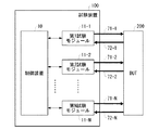
図1は、本実施形態に係る試験装置100の構成を被試験デバイス200と共に示す。本実施形態に係る試験装置100は、制御装置10が、試験モジュールからのアクセス応答を受信しない場合でも、アクセスを発行してから予め定められた検出期間が経過してタイムアウトを検出する前に、その試験モジュールに対する次のアクセスを発行することを目的とする。被試験デバイス200は、例えば、メモリデバイス等であってもよい。
FIG. 1 shows a configuration of a test apparatus 100 according to this embodiment together with a device under
試験装置100は、被試験デバイス200を試験するシステムであってもよい。より詳しくは、試験装置100は、例えば、被試験デバイス200に試験信号を供給して、被試験デバイス200が試験信号に応じて出力する出力信号を期待値と比較することにより、被試験デバイス200の良否を判定してもよい。試験装置100は、制御装置10と複数の試験モジュール11(例えば、11−1〜11−N{Nは正の整数:以下同様})とを備える。
The test apparatus 100 may be a system that tests the device under
制御装置10は、各々の試験モジュール11を制御する。制御装置10は、本実施形態に係る発行側装置の一例である。制御装置10と複数の試験モジュール11との間は、例えば、Gbitイーサネット(登録商標)等の高速通信線で接続されてもよい。制御装置10は、試験の各種設定を目的として、リード(読み出し)アクセスおよびライト(書き込み)アクセスの少なくとも一方のアクセスを試験モジュール11に対して発行する。本実施形態におけるアクセスには、例えば、制御装置10から試験モジュール11にアクセスする時に用いられる信号、コマンドおよびデータ等を含んでいる。
The
試験モジュール11は、制御装置10により発行されたアクセスを受け付ける。試験モジュール11は、本実施形態に係る受付側装置の一例である。複数の試験モジュール11は、各々被試験デバイス200との間で試験入力71及び試験出力72を授受する。例えば、第1試験モジュール11−1は、第1試験入力71−1を被試験デバイス200に送出する一方で、被試験デバイス200から第1試験出力72−1を受信する。同様に、第N試験モジュール11−Nは、第N試験入力71−Nを被試験デバイス200に送出する一方で、被試験デバイス200から第N試験出力72−Nを受信する。
The
図2は、本実施形態に係る制御装置10の構成の一例を示す。制御装置10は、制御処理部21、複数の発行部22(例えば、22−1〜22−N)、複数のアドレスタイムアウト検出部23(例えば、23−1〜23−N)、複数のアクセスタイムアウト検出部24(例えば、24−1〜24−N)、および、複数の応答データ受信部25を有する。
FIG. 2 shows an example of the configuration of the
制御処理部21は、例えば、使用者が実行を指示した試験プログラムを実行する。そして、制御処理部21は、各試験モジュール11の機能・動作を設定するべく試験モジュール11の記憶領域に設定データを書き込む。試験モジュール11の記憶領域は、より具体的には、メモリ領域およびレジスタ領域の少なくとも一方であってもよい。また、これらの記憶領域は、制御装置10側から見た単一のアドレス空間にマッピングされている。また、制御処理部21は、読み出し時に、例えば、試験モジュール11の記憶領域に書き込まれた設定データ、試験結果、及び、診断結果等を読み出す。
For example, the
制御処理部21は、例えば、試験モジュール11が有するメモリまたはレジスタに対して書き込みを行う場合に、アクセス対象となる対象アドレスと書き込みデータを含むライトアクセスのコマンドを出力する。又は、制御処理部21は、例えば、試験モジュール11が有するメモリまたはレジスタに対して読み出しを行う場合に、アクセス対象となる対象アドレスを含むリードアクセスのコマンドを出力する。
For example, when writing to the memory or register of the
複数の発行部22(例えば、22−1〜22−N)、複数のアドレスタイムアウト検出部23、複数のアクセスタイムアウト検出部24、および、複数の応答データ受信部25は、各試験モジュール11に対応して設けられる。例えば、第1試験モジュール11−1には、第1発行部22−1、第1アドレスタイムアウト検出部23−1、第1アクセスタイムアウト検出部24−1、及び第1応答データ受信部25−1が対応して設けられる。同様に、第N試験モジュール11−Nには、第N発行部22−N、第Nアドレスタイムアウト検出部23−N、第Nアクセスタイムアウト検出部24−N、及び第N応答データ受信部25−Nが対応して設けられる。
A plurality of issuing units 22 (for example, 22-1 to 22-N), a plurality of address
発行部22は、制御処理部21から受信したアクセス対象となる対象アドレスを含むアクセス51を試験モジュール11に対して発行する。より具体的には、例えば、発行部22は、複数の試験モジュール11のそれぞれに対して第1のアクセス51を一斉に送信する。
The issuing
また、発行部22は、制御処理部21から入力したアクセス51を、入力順に格納するキュー31を含む。発行部22は、アクセス対象の試験モジュール11が次のアクセスを受付可能になった場合に、キュー31に格納したアクセス51を順次読み出して試験モジュール11に対して発行する。より具体的には、発行部22は、第1のアクセス51を送信したそれぞれの試験モジュール11に対して、第1のアクセス51に対するアドレス応答52のタイムアウトを検出するか、または、第1のアクセス51に対するアクセス応答53を受信したことを条件として、第2のアクセスを発行する。その場合、アドレスタイムアウト検出部23は、第1のアクセス51に対するアドレス応答52のタイムアウトを検出する。アクセスタイムアウト検出部24は、試験モジュール11から次のアクセス51を受付可能となったことを示す、第1のアクセス51に対するアクセス応答53を検出する。本実施形態におけるアドレス応答およびアクセス応答には、例えば、試験モジュール11から制御装置10に、あるアクセスに対して応答する時に用いる信号、コマンド又はデータ等を含んでいる。
The issuing
アドレスタイムアウト検出部23は、試験モジュール11から当該アクセス51の対象アドレスに対応する記憶領域が存在することを示すアドレス応答52を受信する。アドレスタイムアウト検出部23には、アドレス応答52を受信するまでの応答処理の最大値に対して、充分にマージンを持つように、しきい値としてタイムアウト時間が予め設定されてよい。アドレスタイムアウト検出部23は、アドレス応答52を受信するまでの時間およびタイムアウト時間を測定するタイマを有する。例えば、アドレスタイムアウト検出部23は、アドレス応答タイムアウト時間として、制御装置10がアクセス51を発行してから記憶領域を有する試験モジュール11からアドレス応答52を受信するまでの時間より長く、制御装置10がアクセス51を発行してから試験モジュール11からアクセス応答53を受信するまでの時間より短い時間を用いてよい。
The address
アドレスタイムアウト検出部23は、発行部22がアクセス51を発行したときにタイマをスタートさせ、アクセス51を発行してからアドレス応答52を受信するまでの時間を計測する。アドレスタイムアウト検出部23は、例えば、計測結果をタイムアウト時間と比較して、計測結果がタイムアウト時間を超えた場合にタイムアウトを検出する。このようにしてアドレスタイムアウト検出部23は、アクセス51を発行してから予め定められたアドレス応答タイムアウト時間の間に、試験モジュール11からアドレス応答52を受信しなかった場合に、当該アドレス応答52のタイムアウトを検出する。その場合のアドレス応答52は、当該アクセス51の対象アドレスに対応する記憶部70内の記憶領域が存在することを示す。
The address
アクセスタイムアウト検出部24には、試験モジュール11から次のアクセス51を受付可能となったことを示すアクセス応答53を受信するまでの応答処理の最大値に対して、充分にマージンを持つように、アクセス応答53のタイムアウト時間を予め設定されてよい。アクセスタイムアウト検出部24は、アクセス応答53を受信するまでの時間およびタイムアウト時間を測定するタイマを有する。アクセスタイムアウト検出部24は、発行部22がアクセス51を発行したときにタイマをスタートさせ、アクセス応答53を受信するまでの時間を計測する。
The access
アクセスタイムアウト検出部24は、アクセス51に対してアドレス応答52を受信した場合において、所定の条件下で、アクセス51のタイムアウトを検出する。その場合の条件は、当該アクセス51を発行してから、予め定められたアクセス応答タイムアウト時間の間に、試験モジュール11からアクセス応答53を受信しなかったことであってもよい。より具体的には、アクセスタイムアウト検出部24は、例えば、アクセス応答53を受信するまで計測結果を予め定めたタイムアウト時間と比較して、計測結果がタイムアウト時間を超えた場合にタイムアウトを検出する。このようにしてアクセスタイムアウト検出部24は、試験モジュール11からのアクセス応答53を、アクセス応答53のタイムアウト時間までの間に受信しなかった場合に、当該アクセス応答53のタイムアウトを検出する。
The access
応答データ受信部25は、当該アクセス51がリードアクセスである場合、試験モジュール11から読み出されたデータを受信する。応答データ受信部25は、受信したデータを制御処理部21に送出する。
The response
図3は、本実施形態に係る第1試験モジュール11−1の構成の一例を示す。試験モジュール11は、リードアクセスおよびライトアクセスの少なくとも一方のアクセス51を発行する制御装置10により発行されたアクセス51を受け付ける。試験装置100に備えられた複数の試験モジュール11は、それぞれ、他の試験モジュール11にアドレスが割り当てられていないメモリ領域およびレジスタ領域の少なくとも一方を有する。複数の試験モジュール11は、ほぼ同様の構成を有している。以下、複数の試験モジュール11の代表として、第1試験モジュール11−1の構成について説明する。
FIG. 3 shows an example of the configuration of the first test module 11-1 according to the present embodiment. The
第1試験モジュール11−1は、アクセス受信部61−1、アクセス処理部62−1、タイミング発生部63−1、パターン発生部64−1、波形成形部65−1、判定部66−1、アドレス応答送信部67−1、アクセス応答送信部68−1、及び、応答データ送信部69−1を有する。さらにタイミング発生部63−1は、記憶部70a−1を含み、パターン発生部64−1は、記憶部70b−1を含み、波形成形部65−1は、記憶部70c−1を含み、判定部66−1は、記憶部70d−1を含む。また、第1試験モジュール11−1は、例えば、電源部(DPU)およびテストヘッド部(TH)を含んでいても良い。
The first test module 11-1 includes an access reception unit 61-1, an access processing unit 62-1, a timing generation unit 63-1, a pattern generation unit 64-1, a waveform shaping unit 65-1, a determination unit 66-1, It has an address response transmitter 67-1, an access response transmitter 68-1, and a response data transmitter 69-1. Further, the timing generation unit 63-1 includes a
アクセス受信部61−1は、制御装置10の第1発行部22−1からアクセス51−1を受信する。アクセス処理部62−1は、受信したアクセス51−1の対象アドレスに対応する記憶領域に対して、アクセス51−1により指定されたリードまたはライトの処理を実施する。また、アクセス処理部62−1は、アクセス51−1を受信した場合にアクセス51−1の対象アドレスに対応する記憶領域が、当該アクセス処理部62−1のアクセス処理の対象となるタイミング発生部63−1、パターン発生部64−1、波形成形部65−1、判定部66−1内に存在するか否かを検出する。更に、アクセス処理部62−1は、アクセス51−1により指定されたリードまたはライトの処理に対して、例えば、処理コマンドをバッファにキューしたこと、または、当該処理が終了したことを検出する。そしてアクセス処理部62−1は、上記の状態を検出できた場合に、次のアクセスを受けることができることを、アクセス応答送信部68−1に通知する。
The access receiving unit 61-1 receives the access 51-1 from the first issuing unit 22-1 of the
タイミング発生部63−1は、試験パターンを被試験デバイス200へ出力すべきタイミング、及び、被試験デバイス200が出力する第1試験出力72−1をサンプリングすべきタイミングを発生する。具体的には、タイミング発生部63−1は、入力した基準クロックとパターン発生部64−1からのタイミングセット信号により指定されたタイミングデータに基づいて、パターン発生部64−1へ送られる周期信号、波形成形部65−1に送られるタイミング信号、及び、判定部66−1に送られるタイミング信号等を出力する。
The timing generator 63-1 generates a timing at which a test pattern should be output to the device under
パターン発生部64−1は、試験装置100の利用者により指定された試験プログラムのシーケンスを実行して、被試験デバイス200に供給する試験パターン及び期待値を生成する。具体的には、パターン発生部64−1は、周期信号に基づいて、試験パターン及び期待値を出力する。パターン発生部64−1の内部には、試験に先立って試験プログラムが格納される。パターン発生部64−1は、その試験プログラムにしたがって、試験対象のピン毎に個別に試験パターン及び期待値を生成する。
The pattern generator 64-1 executes a test program sequence designated by the user of the test apparatus 100 to generate a test pattern and an expected value to be supplied to the device under
波形成形部65−1は、パターン発生部64−1から試験パターンを受け取ってタイミング発生部63−1が発生したタイミング信号に基づき成形して、被試験デバイス200に供給する第1試験入力71−1を生成する。すなわち、波形成形部65−1は、試験パターンにより指定された信号波形を、タイミング信号により指定されたタイミングで変化するように成形して、第1試験入力71−1として被試験デバイス200に供給する。判定部66−1は、被試験デバイス200の第1試験出力72−1とそれぞれの期待値とを比較する。判定部66−1は、比較結果が不一致(フェイル)の場合、そのアドレスサイクルでフェイル信号(例えば「1」)を出力する。
The waveform shaping unit 65-1 receives the test pattern from the pattern generation unit 64-1, shapes it based on the timing signal generated by the timing generation unit 63-1, and supplies it to the device under
アドレス応答送信部67−1は、所定の条件下で、制御装置10の第1アドレスタイムアウト検出部23−1に対してアドレス応答52−1を送信する。この場合の条件は、当該試験モジュール11−1が、受信したアクセス51−1の対象アドレスに対応する記憶領域を有することであってもよい。アドレス応答送信部67−1は、対象アドレスに対応する記憶領域として、例えば、タイミング発生部63−1内の記憶部70a−1、パターン発生部64−1内の記憶部70b−1、波形成形部65−1内の記憶部70c−1、及び、判定部66−1内の記憶部70d−1のアドレス情報を予め格納してもよい。そして、アドレス応答送信部67−1は、対象アドレスに対応する記憶領域の有無を、例えば、受信した第1アクセス51−1中のアドレスデータと、格納されている記憶部70a−1、記憶部70b−1、記憶部70c−1、及び、記憶部70d−1のアドレス情報を照合することにより判断してもよい。
The address response transmission unit 67-1 transmits an address response 52-1 to the first address timeout detection unit 23-1 of the
アクセス応答送信部68−1は、所定の条件下で、制御装置10の第1アクセスタイムアウト検出部24−1に対してアクセス応答53−1を送信する。この場合の条件は、当該試験モジュール11−1が、受信したアクセス51−1の対象アドレスに対応する記憶領域を有して、かつ、次のアクセス51−1を受付可能となったことであってもよい。また、アクセス応答送信部68−1は、次のアクセス51−1を受付可能となったことを、例えば、アクセス処理部62−1からの通知により判断してもよい。応答データ送信部69−1は、受信したアクセス51−1がリードアクセスである場合、記憶部70a−1、記憶部70b−1、記憶部70c−1、又は、記憶部70d−1からから読み出されたデータを第1応答データ54−1として第1応答データ受信部25−1に送出する。
The access response transmission unit 68-1 transmits an access response 53-1 to the first access timeout detection unit 24-1 of the
以上の構成により、本実施形態の試験装置100は、制御装置10がアクセス応答を受信しない場合に、アクセスを発行してからアドレス応答に対するタイムアウトを検出して、試験モジュール11に対する次のアクセスを発行できる。これにより、本実施形態の試験装置100は、制御装置10から複数の試験モジュール11に対して複数のアクセスを順次発行する場合に、あるアクセスとその次のアクセスの間隔を短縮することができる。
With the above configuration, when the
図4(a)〜(l)は、本実施形態に係る試験装置100が被試験デバイス200に書込/読出試験を行う場合の入出力信号の一例を示す。図4(a)は、発行側装置から受付側装置に出力されるクロック信号の一例を示す。図4(b)は、発行側装置から受付側装置に出力されるライトアクセスにおける対象アドレスデータA1−0〜A1−3および書き込みデータD1−0〜D1−3の一例を示す。各データはクロック信号のエッジに対応して出力される。発行側装置から受付側装置へのアクセスがリードアクセスの場合、発行側装置は、受付側装置に対象アドレスデータA1−0〜A1−3を出力する。
4A to 4L show examples of input / output signals when the test apparatus 100 according to the present embodiment performs a write / read test on the device under
図4(c)は、発行側装置から受付側装置に出力されるコマンドの一例を示す。図4(c)に示したように、発行側装置は、ライトコマンド「0x03」に続けて、受付側装置からアドレス応答で送出すべき信号としての「TAG=1」を送信してもよい。図4(d)は、発行側装置から受付側装置に、アドレスデータの送信がスタートすることを通知するスタート信号の一例を示す。図4(e)は、発行側装置から受付側装置に、有効なアドレスデータが送信されている期間であることを通知するアドレスバリッド信号の一例を示す。 FIG. 4C shows an example of a command output from the issuing side device to the receiving side device. As shown in FIG. 4C, the issuing device may transmit “TAG = 1” as a signal to be transmitted from the receiving device as an address response following the write command “0x03”. FIG. 4D shows an example of a start signal for notifying the transmission of address data from the issuing device to the receiving device. FIG. 4E shows an example of an address valid signal for notifying that the valid address data is being transmitted from the issuing device to the receiving device.
図4(f)は、発行側装置から受付側装置に、ライトコマンドで書き込むべきデータの送信が要求されていることを通知するデータリクエスト信号の一例を示す。図4(g)は、発行側装置から受付側装置に、有効な書き込みデータが送信されている期間であることを通知するデータバリッド信号の一例を示す。図4(h)は、受付側装置となる試験モジュール11の内部で使用されるクロック信号の一例を示す。
FIG. 4F shows an example of a data request signal that notifies the issuing side device that transmission of data to be written by the write command is requested from the issuing side device. FIG. 4G illustrates an example of a data valid signal for notifying that the valid write data is being transmitted from the issuing device to the receiving device. FIG. 4H illustrates an example of a clock signal used inside the
図4(i)は、受付側装置から発行側装置に、対象アドレスに対応する記憶領域が存在することを通知するアドレス応答52−1の一例を示す。受付側装置は、例えば、受信した対象アドレスデータA1−0〜A1−3に対応する記憶領域をアドレス応答送信部67が検出した場合に、アドレス応答送信部67は第1アドレス応答52−1として「TAG=1」をアドレスタイムアウト検出部23に出力してもよい。図4(j)は、受付側装置から発行側装置に、次のアクセスの準備が整ったことを通知するアクセス応答53−1の一例を示す。受付側装置は、受信したアクセスがリードアクセスの場合には、このアクセス応答53−1をリードコマンドで読み出されたデータの送信が始まることを通知する信号として用いてもよい。図4(k)は、受信したアクセスがリードアクセスの場合に、受付側装置から発行側装置に読み出しデータを返信するための信号であるが、ここでは受信したアクセスがライトアクセスの場合であるのでデータは出力されない。
FIG. 4I shows an example of an address response 52-1 that notifies the receiving side device to the issuing side device that a storage area corresponding to the target address exists. For example, when the address response transmission unit 67 detects a storage area corresponding to the received target address data A1-0 to A1-3, the address response transmission unit 67 sets the first address response 52-1. “TAG = 1” may be output to the address
図4(l)は、受付側装置から発行側装置に有効な読み出しデータが送信されている場合に、その期間であることを通知するデータバリッド信号が出力されるが、ここでは受信したアクセスがライトアクセスの場合であるのでデータは出力されない。本実施形態において、アドレス応答期間は、一例として0.5usに設定され、アクセス応答期間は、一例として3.0usに設定されている。 In FIG. 4 (l), when valid read data is transmitted from the receiving side device to the issuing side device, a data valid signal notifying that it is the period is output. Since this is a write access, no data is output. In the present embodiment, the address response period is set to 0.5 us as an example, and the access response period is set to 3.0 us as an example.
図5(b)、(i)、(j)は本実施形態に係る試験装置100が被試験デバイス200に書込/読出試験を行う場合のコマンド発行に対する応答期間とタイムアウト期間の一例を示す。図5(b)は、図4(b)の対象アドレスデータA1−0〜A1−3および書き込みデータD1−0〜D1−3の一例を時間軸方向に縮小して示す。図5(i)は、図4(i)のアドレス応答52−1の一例を時間軸方向に縮小して示す。本例においてアドレス応答期間は、0.5usに設定され、アドレス応答タイムアウト期間は、1usに設定されている。
FIGS. 5B, 5 </ b> I, and 5 </ b> J show an example of a response period and a timeout period for command issuance when the test apparatus 100 according to the present embodiment performs a write / read test on the device under
図5(j)は、図4(j)のアクセス応答53−1の一例を時間軸方向に縮小して示す。本例において、アクセス応答期間は、3.0usに設定され、アクセス応答タイムアウト期間は、6.0usに設定されている。 FIG. 5J shows an example of the access response 53-1 of FIG. 4J reduced in the time axis direction. In this example, the access response period is set to 3.0 us, and the access response timeout period is set to 6.0 us.
図4(i)、図4(j)、図5(i)、および、図5(j)に示したように本実施形態では、試験モジュール11が、受信したアクセス51の対象アドレスに対応する記憶領域を有する場合には、アドレス応答送信部67は、アクセス応答送信部68が当該アクセス51に対するアクセス応答53を送信する前に、当該アクセス51に対するアドレス応答52を送信する。また、図5(j)の下に示したようにアクセスタイムアウト検出部24は、アクセス51に対してアドレス応答52を受信した場合に、アクセス51のタイムアウトを検出する。アドレス応答タイムアウト時間は、アクセス応答タイムアウト時間と比較し短い。例えば、アドレス応答タイムアウト時間は、上記のように1us程度に設定され、アクセス応答タイムアウト時間は、上記のように6us程度に設定されている。
As shown in FIGS. 4 (i), 4 (j), 5 (i), and 5 (j), in this embodiment, the
図6(a)〜(d)は、各々キュー内の4番目のアクセス発行までの期間の一例を示す。図6(a)は、試験装置100がアドレス応答タイムアウト機能を有していない場合で、第1試験モジュール11−1にアクセスを発行する第1キュー31−1を示す。第1キュー31−1には、4個のアクセスが格納されている。第1キュー31−1中では、4個のアクセスのうち2番目のアクセスだけが第1試験モジュール11−1内の記憶領域に対応する対象アドレスを有する。この場合、4番目のアクセスを実行するまでの期間は、1番目のアクセス対するアクセス応答タイムアウトの6usと、2番目のアクセスに対するアクセス応答の3usと、3番目のアクセスに対するアクセス応答タイムアウトの6usを加算した15usになる。 FIGS. 6A to 6D each show an example of the period until the fourth access issuance in the queue. FIG. 6A shows the first queue 31-1 that issues access to the first test module 11-1 when the test apparatus 100 does not have an address response timeout function. Four accesses are stored in the first queue 31-1. In the first queue 31-1, only the second access among the four accesses has a target address corresponding to the storage area in the first test module 11-1. In this case, for the period until the fourth access is executed, 6us of the access response timeout for the first access, 3us of the access response for the second access, and 6us of the access response timeout for the third access are added. 15us.
図6(b)は、試験装置100がアドレス応答タイムアウト機能を有していない場合で、第2試験モジュール11−2にアクセスを発行する第2キュー31−2を示す。第2キュー31−2には、4個のアクセスが格納されている。第2キュー31−2中では、4個のアクセスのうち1番目と3番目のアクセスが第2試験モジュール11−2内の記憶領域に対応する対象アドレスを有する。この場合、4番目のアクセスを実行するまでの期間は、1番目のアクセス対するアクセス応答の3usと、2番目のアクセスに対するアクセス応答タイムアウトの6usと、3番目のアクセスに対するアクセス応答の3usを加算した12usになる。 FIG. 6B shows the second queue 31-2 that issues an access to the second test module 11-2 when the test apparatus 100 does not have the address response timeout function. Four accesses are stored in the second queue 31-2. In the second queue 31-2, the first and third accesses out of the four accesses have target addresses corresponding to the storage areas in the second test module 11-2. In this case, for the period until the fourth access is executed, 3us of the access response for the first access, 6us of the access response timeout for the second access, and 3us of the access response for the third access are added. 12us.
図6(c)は、試験装置100がアドレス応答タイムアウト機能を有する場合で、第1試験モジュール11−1にアクセスを発行する第1キュー31−1を示す。第1キュー31−1には、4個のアクセスが格納されている。第1キュー31−1中では、4個のアクセスのうち2番目のアクセスだけが第1試験モジュール11−1内の記憶領域に対応する対象アドレスを有する。この場合、4番目のアクセスを実行するまでの期間は、1番目のアクセス対するアドレス応答タイムアウトの1usと、2番目のアクセスに対するアクセス応答の3usと、3番目のアクセスに対するアドレス応答タイムアウトの1usを加算した5usになる。 FIG. 6C shows the first queue 31-1 that issues access to the first test module 11-1 when the test apparatus 100 has an address response timeout function. Four accesses are stored in the first queue 31-1. In the first queue 31-1, only the second access among the four accesses has a target address corresponding to the storage area in the first test module 11-1. In this case, for the period until the fourth access is executed, 1 us of the address response timeout for the first access, 3 us of the access response for the second access, and 1 us of the address response timeout for the third access are added. 5us.
図6(d)は、試験装置100がアドレス応答タイムアウト機能を有する場合で、第2試験モジュール11−2にアクセスを発行する第2キュー31−2を示す。第2キュー31−2には、4個のアクセスが格納されている。第2キュー31−2中では、4個のアクセスのうち1番目と3番目のアクセスが第2試験モジュール11−2内の記憶領域に対応する対象アドレスを有する。この場合、4番目のアクセスを実行するまでの期間は、1番目のアクセス対するアクセス応答の3usと、2番目のアクセスに対するアドレス応答タイムアウトの1usと、3番目のアクセスに対するアクセス応答の3usを加算した7usになる。 FIG. 6D shows a second queue 31-2 that issues an access to the second test module 11-2 when the test apparatus 100 has an address response timeout function. Four accesses are stored in the second queue 31-2. In the second queue 31-2, the first and third accesses out of the four accesses have target addresses corresponding to the storage areas in the second test module 11-2. In this case, 3us of the access response for the first access, 1us of the address response timeout for the second access, and 3us of the access response for the third access are added to the period until the fourth access is executed. 7 us.
図6(a)と図6(c)を比較した場合、アドレス応答タイムアウトを備える場合の第1試験モジュール11−1では、第4番目のアドレスを実行するまでの時間が15usから5usに短縮されている。また、図6(b)と図6(d)を比較した場合、アドレス応答タイムアウトを備える場合の第2試験モジュール11−2では、第4番目のアドレスを実行するまでの時間が12usから7usに短縮されている。 When comparing FIG. 6A and FIG. 6C, in the first test module 11-1 having an address response timeout, the time until the fourth address is executed is reduced from 15 us to 5 us. ing. Further, when comparing FIG. 6B and FIG. 6D, in the second test module 11-2 when the address response timeout is provided, the time until the fourth address is executed is changed from 12 us to 7 us. It has been shortened.
図7は、本実施形態に係る制御装置10として機能するコンピュータ600のハードウェア構成の一例を示す。コンピュータ600は、ホストコントローラ1082により相互に接続されるCPU1000、RAM1020、及びグラフィックコントローラ1075を有するCPU周辺部と、入出力コントローラ1084によりホストコントローラ1082に接続される通信インターフェイス1030、ハードディスクドライブ1040、及びCD−ROMドライブ1060を有する入出力部と、入出力コントローラ1084に接続されるROM1010、フレキシブルディスクドライブ1050、及び入出力チップ1070を有するレガシー入出力部とを備える。
FIG. 7 shows an example of a hardware configuration of a computer 600 that functions as the
ホストコントローラ1082は、RAM1020と、高い転送レートでRAM1020をアクセスするCPU1000及びグラフィックコントローラ1075とを接続する。CPU1000は、ROM1010及びRAM1020に格納されたプログラムに基づいて動作して、各部の制御を行う。グラフィックコントローラ1075は、CPU1000等がRAM1020内に設けたフレームバッファ上に生成する画像データを取得して、表示装置1080上に表示させる。これに代えて、グラフィックコントローラ1075は、CPU1000等が生成する画像データを格納するフレームバッファを、内部に含んでもよい。 The host controller 1082 connects the RAM 1020 to the CPU 1000 and the graphic controller 1075 that access the RAM 1020 at a high transfer rate. The CPU 1000 operates based on programs stored in the ROM 1010 and the RAM 1020 to control each unit. The graphic controller 1075 acquires image data generated by the CPU 1000 or the like on a frame buffer provided in the RAM 1020 and displays it on the display device 1080. Alternatively, the graphic controller 1075 may include a frame buffer that stores image data generated by the CPU 1000 or the like.
入出力コントローラ1084は、ホストコントローラ1082と、比較的高速な入出力装置である通信インターフェイス1030、ハードディスクドライブ1040、及びCD−ROMドライブ1060を接続する。通信インターフェイス1030は、ネットワークを介して外部の装置と通信する。ハードディスクドライブ1040は、コンピュータ600が使用するプログラム及びデータを格納する。CD−ROMドライブ1060は、CD−ROMディスク1095からプログラム又はデータを読み取り、RAM1020又はハードディスクドライブ1040に提供する。 The input / output controller 1084 connects the host controller 1082 to the communication interface 1030, the hard disk drive 1040, and the CD-ROM drive 1060, which are relatively high-speed input / output devices. The communication interface 1030 communicates with an external device via a network. The hard disk drive 1040 stores programs and data used by the computer 600. The CD-ROM drive 1060 reads a program or data from a CD-ROM disk 1095 and provides it to the RAM 1020 or the hard disk drive 1040.
また、入出力コントローラ1084には、ROM1010と、フレキシブルディスクドライブ1050又は入出力チップ1070等の比較的低速な入出力装置とが接続される。ROM1010は、コンピュータ600の起動時にCPU1000が実行するブートプログラム、又はコンピュータ600のハードウェアに依存するプログラム等を格納する。フレキシブルディスクドライブ1050は、フレキシブルディスク1090からプログラム又はデータを読み取り、入出力チップ1070を介してRAM1020またはハードディスクドライブ1040に提供する。入出力チップ1070は、フレキシブルディスク1090、又は、例えばパラレルポート、シリアルポート、キーボードポート、マウスポート等を介して各種の入出力装置を接続する。 The input / output controller 1084 is connected to the ROM 1010 and a relatively low-speed input / output device such as the flexible disk drive 1050 or the input / output chip 1070. The ROM 1010 stores a boot program executed by the CPU 1000 when the computer 600 is started up, a program depending on the hardware of the computer 600, and the like. The flexible disk drive 1050 reads a program or data from the flexible disk 1090 and provides it to the RAM 1020 or the hard disk drive 1040 via the input / output chip 1070. The input / output chip 1070 connects various input / output devices via a flexible disk 1090 or, for example, a parallel port, a serial port, a keyboard port, a mouse port, and the like.
コンピュータ600に提供されるプログラムは、フレキシブルディスク1090、CD−ROMディスク1095、又はICカード等の記録媒体に格納されて利用者によって提供される。プログラムは、入出力チップ1070及び/又は入出力コントローラ1084を介して、記録媒体から読み出されコンピュータ600にインストールされて実行される。プログラムがコンピュータ600等に働きかけて行わせる動作は、図1から図6において説明した制御装置10における動作と同一であるから、説明を省略する。
The program provided to the computer 600 is stored in a recording medium such as the flexible disk 1090, the CD-ROM disk 1095, or an IC card and provided by the user. The program is read from the recording medium via the input / output chip 1070 and / or the input / output controller 1084, installed in the computer 600, and executed. The operation that the program causes the computer 600 or the like to perform is the same as the operation in the
制御装置10にインストールされて実行され、試験装置100の機能を制御するプログラムは、試験モジュール11を制御して、試験装置100に上記した動作を実施させる内容を含む。
The program that is installed and executed in the
以上に示したプログラムは、外部の記憶媒体に格納されてもよい。記憶媒体としては、フレキシブルディスク1090、CD−ROMディスク1095の他に、DVD又はPD等の光学記録媒体、MD等の光磁気記録媒体、テープ媒体、ICカード等の半導体メモリ等を用いることができる。また、専用通信ネットワーク又はインターネットに接続されたサーバシステムに設けたハードディスク又はRAM等の記憶装置を記録媒体として使用して、ネットワークを介してプログラムをコンピュータ600に提供してもよい。 The program shown above may be stored in an external storage medium. As the storage medium, in addition to the flexible disk 1090 and the CD-ROM disk 1095, an optical recording medium such as DVD or PD, a magneto-optical recording medium such as MD, a tape medium, a semiconductor memory such as an IC card, and the like can be used. . Further, a storage device such as a hard disk or a RAM provided in a server system connected to a dedicated communication network or the Internet may be used as a recording medium, and the program may be provided to the computer 600 via the network.
このように本実施形態の試験装置100は、制御装置10がアクセス応答を受信しない場合に、アクセスを発行してからアドレス応答に対するタイムアウトを検出するまでの期間で、試験モジュール11に対する次のアクセスを発行でき、また、試験装置100は、複数の試験モジュール11に発行するあるアクセスとその次のアクセスの間隔を短縮することができる。
As described above, when the
以上、本発明を実施の形態を用いて説明したが、本発明の技術的範囲は上記実施の形態に記載の範囲には限定されない。上記実施の形態に、多様な変更または改良を加えることが可能であることが当業者に明らかである。その様な変更または改良を加えた形態も本発明の技術的範囲に含まれ得ることが、請求の範囲の記載から明らかである。例えば、本実施形態に記載した発行側装置及び受付側装置の間の通信プロトコルは、試験装置内に限られず、アクセスを発行する各種の装置及びアクセスを受信する各種の装置に適用可能である。 As mentioned above, although this invention was demonstrated using embodiment, the technical scope of this invention is not limited to the range as described in the said embodiment. It will be apparent to those skilled in the art that various modifications or improvements can be added to the above-described embodiment. It is apparent from the scope of the claims that the embodiments added with such changes or improvements can be included in the technical scope of the present invention. For example, the communication protocol between the issuing device and the receiving device described in the present embodiment is not limited to the test device, and can be applied to various devices that issue access and various devices that receive access.
Claims (8)
前記発行側装置は、
アクセス対象となる対象アドレスを含むアクセスを前記受付側装置に対して発行する発行部と、
前記アクセスを発行してから予め定められたアドレス応答タイムアウト時間の間に、前記受付側装置から、当該アクセスの対象アドレスに対応する記憶領域が存在することを示すアドレス応答を受信しなかった場合に、当該アドレス応答のタイムアウトを検出するアドレスタイムアウト検出部と
を有し、
前記発行部は、前記アクセスを発行してから予め定められたアクセス応答タイムアウト時間の間に、前記アクセス応答タイムアウトよりもタイムアウト時間が短い前記アドレス応答のタイムアウトが検出された場合、または、前記受付側装置から次のアクセスを受付可能となったことを示すアクセス応答を受信したことに応じて次のアクセスを前記受付側装置に対して発行し、
前記受付側装置は、
前記発行側装置から前記アクセスを受信するアクセス受信部と、
当該受付側装置が、受信した前記アクセスの対象アドレスに対応する記憶領域を有することを条件として、前記発行側装置に対して前記アドレス応答を送信するアドレス応答送信部と、
受信した前記アクセスの対象アドレスに対応する記憶領域に対し、前記アクセスにより指定されたリードまたはライトを処理するアクセス処理部と、
当該受付側装置が、受信した前記アクセスの対象アドレスに対応する記憶領域を有し、かつ、次の前記アクセスを受付可能となったことを条件として、前記発行側装置に対して前記アクセス応答を送信するアクセス応答送信部と
を有するシステム。A system comprising an issuer device that issues at least one of read access and write access, and a reception device that accepts an access issued by the issuer device,
The issuing device is:
An issuing unit that issues an access including a target address to be accessed to the reception-side device;
When an address response indicating that there is a storage area corresponding to the access target address is not received from the accepting side device during a predetermined address response timeout period after the access is issued And an address timeout detection unit for detecting a timeout of the address response,
The issuing unit detects a time-out of the address response that is shorter than the access response time-out during a predetermined access response time-out time after issuing the access , or the receiving side In response to receiving an access response indicating that the next access can be accepted from the device, the next access is issued to the accepting device,
The reception side device is:
An access receiver for receiving the access from the issuing device;
An address response transmission unit that transmits the address response to the issuing side device on the condition that the receiving side device has a storage area corresponding to the received target address of the access;
An access processing unit that processes the read or write specified by the access to the storage area corresponding to the received target address;
On the condition that the accepting side device has a storage area corresponding to the received access target address and can accept the next access, the access side response is sent to the issuing side device. And an access response transmission unit for transmitting.
前記アドレス応答タイムアウト時間は、前記アクセス応答タイムアウト時間と比較し短い請求項2に記載のシステム。The issuing apparatus, when receiving the address in response to the access, during the access response timeout time predetermined from issuing the access, receives the access response from the reception side apparatus An access time-out detection unit for detecting the access time-out on condition that
The system according to claim 2, wherein the address response timeout time is shorter than the access response timeout time.
前記複数の受付側装置のそれぞれは、他の前記受付側装置にアドレスが割り当てられていないメモリ領域およびレジスタ領域の少なくとも一方を有し、
前記発行部は、
第1の前記アクセスを前記複数の受付側装置のそれぞれに対して送信し、
それぞれの前記受付側装置に対し、前記第1のアクセスに対する前記アドレス応答のタイムアウトを検出し、または、前記第1のアクセスに対する前記アクセス応答を受信したことを条件として、第2の前記アクセスを発行する
請求項3に記載のシステム。A plurality of the reception side devices;
Each of the plurality of reception side devices has at least one of a memory area and a register area in which no address is assigned to the other reception side devices,
The issuing unit
Transmitting the first access to each of the plurality of reception side devices;
The second access is issued on the condition that a timeout of the address response to the first access is detected or the access response to the first access is received for each accepting device The system according to claim 3.
アクセス対象となる対象アドレスを含むアクセスを前記受付側装置に対して発行する発行部と、
前記アクセスを発行してから予め定められたアドレス応答タイムアウト時間の間に、前記受付側装置から、当該アクセスの対象アドレスに対応する記憶領域が存在することを示すアドレス応答を受信しなかった場合に、当該アドレス応答のタイムアウトを検出するアドレスタイムアウト検出部と
を備え、
前記発行部は、前記アクセスを発行してから予め定められたアクセス応答タイムアウト時間の間に、前記アクセス応答タイムアウトよりもタイムアウト時間が短い前記アドレス応答のタイムアウトが検出された場合、または、前記受付側装置から次のアクセスを受付可能となったことを示すアクセス応答を受信したことに応じて次のアクセスを前記受付側装置に対して発行する
発行側装置。An issuing device that issues at least one of read access and write access to a receiving device;
An issuing unit that issues an access including a target address to be accessed to the reception-side device;
When an address response indicating that there is a storage area corresponding to the access target address is not received from the accepting side device during a predetermined address response timeout period after the access is issued And an address timeout detection unit for detecting the timeout of the address response,
The issuing unit detects a time-out of the address response that is shorter than the access response time-out during a predetermined access response time-out time after issuing the access , or the receiving side An issuing device that issues a next access to the receiving device in response to receiving an access response indicating that the next access can be received from the device.
前記発行側装置から前記アクセスを受信するアクセス受信部と、
当該受付側装置が、受信した前記アクセスの対象アドレスに対応する記憶領域を有することを条件として、前記発行側装置に対してアドレス応答を送信するアドレス応答送信部と、
受信した前記アクセスの対象アドレスに対応する記憶領域に対し、前記アクセスにより指定されたリードまたはライトを処理するアクセス処理部と、
当該受付側装置が、受信した前記アクセスの対象アドレスに対応する記憶領域を有し、かつ、次の前記アクセスを受付可能となったことを条件として、前記発行側装置に対して前記受付側装置から次のアクセスを受付可能となったことを示すアクセス応答を送信するアクセス応答送信部と
を備える受付側装置。A receiving-side device that accepts an access issued by an issuing-side device that issues at least one of read access and write access;
An access receiver for receiving the access from the issuing device;
An address response transmitting unit that transmits an address response to the issuing side device on the condition that the receiving side device has a storage area corresponding to the received target address of the access;
An access processing unit that processes the read or write specified by the access to the storage area corresponding to the received target address;
On the condition that the accepting side device has a storage area corresponding to the received access target address and can accept the next access, the accepting side device can receive the access side device. An access response transmission unit that transmits an access response indicating that the next access can be received from the reception side device.
前記制御装置は、
前記試験モジュールが有するメモリまたはレジスタに対し、読み出しまたは書き込みの少なくとも一方を行う場合において、アクセス対象となる対象アドレスを含むアクセスを前記試験モジュールに対して発行する発行部と、
前記アクセスを発行してから予め定められたアドレス応答タイムアウト時間の間に、前記試験モジュールから、当該アクセスの対象アドレスに対応する記憶領域が存在することを示すアドレス応答を受信しなかった場合に、当該アドレス応答のタイムアウトを検出するアドレスタイムアウト検出部と
を有し、前記発行部は、前記アクセスを発行してから予め定められたアクセス応答タイムアウト時間の間に、前記アクセス応答タイムアウトよりもタイムアウト時間が短い前記アドレス応答のタイムアウトが検出された場合、または、前記試験モジュールから次のアクセスを受付可能となったことを示すアクセス応答を受信したことに応じて次のアクセスを前記試験モジュールに対して発行し、
前記試験モジュールは、
前記制御装置から前記アクセスを受信するアクセス受信部と、
当該試験モジュールが、受信した前記アクセスの対象アドレスに対応する記憶領域を有することを条件として、前記制御装置に対して前記アドレス応答を送信するアドレス応答送信部と、
受信した前記アクセスの対象アドレスに対応する記憶領域に対し、前記アクセスにより指定されたリードまたはライトを処理するアクセス処理部と、
当該試験モジュールが、受信した前記アクセスの対象アドレスに対応する記憶領域を有し、かつ、次の前記アクセスを受付可能となったことを条件として、前記制御装置に対して前記アクセス応答を送信するアクセス応答送信部と
を有する試験装置。A test apparatus for testing the device under test, comprising: a test module that exchanges signals with the device under test; and a control device that controls the test module;
The controller is
An issuing unit that issues an access including a target address to be accessed to the test module when performing at least one of reading and writing to a memory or a register included in the test module;
When an address response indicating that a storage area corresponding to the access target address exists is not received from the test module during a predetermined address response timeout period after issuing the access, An address timeout detection unit for detecting a timeout of the address response, wherein the issuing unit issues a timeout time longer than the access response timeout during a predetermined access response timeout time after issuing the access. Issuing the next access to the test module when a short timeout of the address response is detected, or in response to receiving an access response indicating that the next access can be accepted from the test module And
The test module is
An access receiver for receiving the access from the control device;
An address response transmission unit that transmits the address response to the control device on the condition that the test module has a storage area corresponding to the received target address of the access;
An access processing unit that processes the read or write specified by the access to the storage area corresponding to the received target address;
The test module transmits the access response to the control device on the condition that the test module has a storage area corresponding to the received access target address and can accept the next access. A test apparatus comprising: an access response transmission unit.
Applications Claiming Priority (1)
| Application Number | Priority Date | Filing Date | Title |
|---|---|---|---|
| PCT/JP2007/065557 WO2009019777A1 (en) | 2007-08-08 | 2007-08-08 | System, issuing end device, receiving end device, and tester |
Publications (2)
| Publication Number | Publication Date |
|---|---|
| JPWO2009019777A1 JPWO2009019777A1 (en) | 2010-10-28 |
| JP5113842B2 true JP5113842B2 (en) | 2013-01-09 |
Family
ID=40341025
Family Applications (1)
| Application Number | Title | Priority Date | Filing Date |
|---|---|---|---|
| JP2009526304A Expired - Fee Related JP5113842B2 (en) | 2007-08-08 | 2007-08-08 | System, issuing device, receiving device, and testing device |
Country Status (2)
| Country | Link |
|---|---|
| JP (1) | JP5113842B2 (en) |
| WO (1) | WO2009019777A1 (en) |
Citations (4)
| Publication number | Priority date | Publication date | Assignee | Title |
|---|---|---|---|---|
| JPH03225546A (en) * | 1990-01-31 | 1991-10-04 | Oki Electric Ind Co Ltd | Method for confirming whether option board is mounted or not |
| JPH09325919A (en) * | 1996-06-06 | 1997-12-16 | Nec Eng Ltd | Split transfer error monitoring device |
| JP2003058323A (en) * | 2001-08-20 | 2003-02-28 | Nec Corp | Disk array device, its data transfer method, data transfer program |
| JP2006113798A (en) * | 2004-10-14 | 2006-04-27 | Ricoh Co Ltd | Data transfer system, reception buffer device, method for setting specification of data transfer system and image formation system |
-
2007
- 2007-08-08 WO PCT/JP2007/065557 patent/WO2009019777A1/en active Application Filing
- 2007-08-08 JP JP2009526304A patent/JP5113842B2/en not_active Expired - Fee Related
Patent Citations (4)
| Publication number | Priority date | Publication date | Assignee | Title |
|---|---|---|---|---|
| JPH03225546A (en) * | 1990-01-31 | 1991-10-04 | Oki Electric Ind Co Ltd | Method for confirming whether option board is mounted or not |
| JPH09325919A (en) * | 1996-06-06 | 1997-12-16 | Nec Eng Ltd | Split transfer error monitoring device |
| JP2003058323A (en) * | 2001-08-20 | 2003-02-28 | Nec Corp | Disk array device, its data transfer method, data transfer program |
| JP2006113798A (en) * | 2004-10-14 | 2006-04-27 | Ricoh Co Ltd | Data transfer system, reception buffer device, method for setting specification of data transfer system and image formation system |
Also Published As
| Publication number | Publication date |
|---|---|
| WO2009019777A1 (en) | 2009-02-12 |
| JPWO2009019777A1 (en) | 2010-10-28 |
Similar Documents
| Publication | Publication Date | Title |
|---|---|---|
| TWI436204B (en) | Testing system and method for usb hub | |
| KR20130042370A (en) | Test method for ufs interface and memory device testing by the same method | |
| KR20140035776A (en) | Embedded multimedia card(emmc), host for controlling the emmc, and methods for operating the emmc and the host | |
| US20070088874A1 (en) | Offload engine as processor peripheral | |
| KR20140035774A (en) | Embedded multimedia card(emmc), host for controlling the emmc, and methods for operating the emmc and the host | |
| JP2014059876A (en) | Host that controls nonvolatile memory card, system that includes the same, and operation method of the same | |
| US9330031B2 (en) | System and method for calibration of serial links using a serial-to-parallel loopback | |
| CN110941578B (en) | LIO design method and device with DMA function | |
| JPWO2007114373A1 (en) | Test method, test system and auxiliary board | |
| US8811111B2 (en) | Memory controller with reduced power consumption, memory device, and memory system | |
| US20090094432A1 (en) | Memory access control device, command issuing device, and method | |
| US6820149B2 (en) | Method, system, and program for testing a bus interface | |
| CN105356988A (en) | PCIe based full duplex DMA transmission method | |
| WO2019128987A1 (en) | Bitwise writing apparatus for system-on-chip system | |
| JP5113842B2 (en) | System, issuing device, receiving device, and testing device | |
| TW201344444A (en) | Motherboard and data processing method thereof | |
| CN111949585A (en) | Data conversion processing method and device | |
| US10976960B2 (en) | Methods of synchronizing memory operations and memory systems employing the same | |
| CN114721983B (en) | DDR4 accelerating read-write device | |
| JP5080580B2 (en) | System, relay device, and test device | |
| KR20080065873A (en) | Apparatus and method for tracing descriptors in host controllers | |
| TW201324174A (en) | Information communication system and method | |
| CN106055505A (en) | Optical module and transmission method of data in optical module | |
| US8694839B2 (en) | Method and system for testing chips | |
| CN101976230A (en) | Transaction translator of universal serial bus and input request isochronous transaction method |
Legal Events
| Date | Code | Title | Description |
|---|---|---|---|
| A131 | Notification of reasons for refusal |
Free format text: JAPANESE INTERMEDIATE CODE: A131 Effective date: 20120221 |
|
| A521 | Request for written amendment filed |
Free format text: JAPANESE INTERMEDIATE CODE: A523 Effective date: 20120410 |
|
| TRDD | Decision of grant or rejection written | ||
| A01 | Written decision to grant a patent or to grant a registration (utility model) |
Free format text: JAPANESE INTERMEDIATE CODE: A01 Effective date: 20121002 |
|
| A01 | Written decision to grant a patent or to grant a registration (utility model) |
Free format text: JAPANESE INTERMEDIATE CODE: A01 |
|
| A61 | First payment of annual fees (during grant procedure) |
Free format text: JAPANESE INTERMEDIATE CODE: A61 Effective date: 20121012 |
|
| FPAY | Renewal fee payment (event date is renewal date of database) |
Free format text: PAYMENT UNTIL: 20151019 Year of fee payment: 3 |
|
| R150 | Certificate of patent or registration of utility model |
Free format text: JAPANESE INTERMEDIATE CODE: R150 |
|
| LAPS | Cancellation because of no payment of annual fees |