JP5112468B2 - Error detection and correction circuit, memory controller, and semiconductor memory device - Google Patents
Error detection and correction circuit, memory controller, and semiconductor memory device Download PDFInfo
- Publication number
- JP5112468B2 JP5112468B2 JP2010073411A JP2010073411A JP5112468B2 JP 5112468 B2 JP5112468 B2 JP 5112468B2 JP 2010073411 A JP2010073411 A JP 2010073411A JP 2010073411 A JP2010073411 A JP 2010073411A JP 5112468 B2 JP5112468 B2 JP 5112468B2
- Authority
- JP
- Japan
- Prior art keywords
- error detection
- correction circuit
- address
- unit
- variable
- Prior art date
- Legal status (The legal status is an assumption and is not a legal conclusion. Google has not performed a legal analysis and makes no representation as to the accuracy of the status listed.)
- Expired - Fee Related
Links
Images


Classifications
-
- G—PHYSICS
- G06—COMPUTING; CALCULATING OR COUNTING
- G06F—ELECTRIC DIGITAL DATA PROCESSING
- G06F11/00—Error detection; Error correction; Monitoring
- G06F11/07—Responding to the occurrence of a fault, e.g. fault tolerance
- G06F11/08—Error detection or correction by redundancy in data representation, e.g. by using checking codes
- G06F11/10—Adding special bits or symbols to the coded information, e.g. parity check, casting out 9's or 11's
- G06F11/1008—Adding special bits or symbols to the coded information, e.g. parity check, casting out 9's or 11's in individual solid state devices
- G06F11/1048—Adding special bits or symbols to the coded information, e.g. parity check, casting out 9's or 11's in individual solid state devices using arrangements adapted for a specific error detection or correction feature
-
- H—ELECTRICITY
- H03—ELECTRONIC CIRCUITRY
- H03M—CODING; DECODING; CODE CONVERSION IN GENERAL
- H03M13/00—Coding, decoding or code conversion, for error detection or error correction; Coding theory basic assumptions; Coding bounds; Error probability evaluation methods; Channel models; Simulation or testing of codes
- H03M13/03—Error detection or forward error correction by redundancy in data representation, i.e. code words containing more digits than the source words
- H03M13/05—Error detection or forward error correction by redundancy in data representation, i.e. code words containing more digits than the source words using block codes, i.e. a predetermined number of check bits joined to a predetermined number of information bits
- H03M13/11—Error detection or forward error correction by redundancy in data representation, i.e. code words containing more digits than the source words using block codes, i.e. a predetermined number of check bits joined to a predetermined number of information bits using multiple parity bits
- H03M13/1102—Codes on graphs and decoding on graphs, e.g. low-density parity check [LDPC] codes
- H03M13/1105—Decoding
- H03M13/1111—Soft-decision decoding, e.g. by means of message passing or belief propagation algorithms
- H03M13/1117—Soft-decision decoding, e.g. by means of message passing or belief propagation algorithms using approximations for check node processing, e.g. an outgoing message is depending on the signs and the minimum over the magnitudes of all incoming messages according to the min-sum rule
-
- H—ELECTRICITY
- H03—ELECTRONIC CIRCUITRY
- H03M—CODING; DECODING; CODE CONVERSION IN GENERAL
- H03M13/00—Coding, decoding or code conversion, for error detection or error correction; Coding theory basic assumptions; Coding bounds; Error probability evaluation methods; Channel models; Simulation or testing of codes
- H03M13/03—Error detection or forward error correction by redundancy in data representation, i.e. code words containing more digits than the source words
- H03M13/05—Error detection or forward error correction by redundancy in data representation, i.e. code words containing more digits than the source words using block codes, i.e. a predetermined number of check bits joined to a predetermined number of information bits
- H03M13/11—Error detection or forward error correction by redundancy in data representation, i.e. code words containing more digits than the source words using block codes, i.e. a predetermined number of check bits joined to a predetermined number of information bits using multiple parity bits
- H03M13/1102—Codes on graphs and decoding on graphs, e.g. low-density parity check [LDPC] codes
- H03M13/1105—Decoding
- H03M13/1131—Scheduling of bit node or check node processing
- H03M13/1137—Partly parallel processing, i.e. sub-blocks or sub-groups of nodes being processed in parallel
-
- H—ELECTRICITY
- H03—ELECTRONIC CIRCUITRY
- H03M—CODING; DECODING; CODE CONVERSION IN GENERAL
- H03M13/00—Coding, decoding or code conversion, for error detection or error correction; Coding theory basic assumptions; Coding bounds; Error probability evaluation methods; Channel models; Simulation or testing of codes
- H03M13/03—Error detection or forward error correction by redundancy in data representation, i.e. code words containing more digits than the source words
- H03M13/05—Error detection or forward error correction by redundancy in data representation, i.e. code words containing more digits than the source words using block codes, i.e. a predetermined number of check bits joined to a predetermined number of information bits
- H03M13/11—Error detection or forward error correction by redundancy in data representation, i.e. code words containing more digits than the source words using block codes, i.e. a predetermined number of check bits joined to a predetermined number of information bits using multiple parity bits
- H03M13/1102—Codes on graphs and decoding on graphs, e.g. low-density parity check [LDPC] codes
- H03M13/1148—Structural properties of the code parity-check or generator matrix
- H03M13/116—Quasi-cyclic LDPC [QC-LDPC] codes, i.e. the parity-check matrix being composed of permutation or circulant sub-matrices
-
- H—ELECTRICITY
- H03—ELECTRONIC CIRCUITRY
- H03M—CODING; DECODING; CODE CONVERSION IN GENERAL
- H03M13/00—Coding, decoding or code conversion, for error detection or error correction; Coding theory basic assumptions; Coding bounds; Error probability evaluation methods; Channel models; Simulation or testing of codes
- H03M13/03—Error detection or forward error correction by redundancy in data representation, i.e. code words containing more digits than the source words
- H03M13/05—Error detection or forward error correction by redundancy in data representation, i.e. code words containing more digits than the source words using block codes, i.e. a predetermined number of check bits joined to a predetermined number of information bits
- H03M13/11—Error detection or forward error correction by redundancy in data representation, i.e. code words containing more digits than the source words using block codes, i.e. a predetermined number of check bits joined to a predetermined number of information bits using multiple parity bits
- H03M13/1102—Codes on graphs and decoding on graphs, e.g. low-density parity check [LDPC] codes
- H03M13/1148—Structural properties of the code parity-check or generator matrix
- H03M13/118—Parity check matrix structured for simplifying encoding, e.g. by having a triangular or an approximate triangular structure
- H03M13/1185—Parity check matrix structured for simplifying encoding, e.g. by having a triangular or an approximate triangular structure wherein the parity-check matrix comprises a part with a double-diagonal
- H03M13/1188—Parity check matrix structured for simplifying encoding, e.g. by having a triangular or an approximate triangular structure wherein the parity-check matrix comprises a part with a double-diagonal wherein in the part with the double-diagonal at least one column has an odd column weight equal or greater than three
Description
本発明は、LDPC符号化されたデータを復号処理する誤り検出訂正回路、前記誤り検出訂正回路を有するメモリコントローラ、および前記誤り検出訂正回路を有する半導体メモリ装置に関し、特に部分並列処理を行う誤り検出訂正回路、前記誤り検出訂正回路を有するメモリコントローラ、および前記誤り検出訂正回路を有する半導体メモリ装置に関する。 The present invention relates to an error detection / correction circuit for decoding LDPC-encoded data, a memory controller having the error detection / correction circuit, and a semiconductor memory device having the error detection / correction circuit, and in particular, error detection for performing partial parallel processing. The present invention relates to a correction circuit, a memory controller having the error detection and correction circuit, and a semiconductor memory device having the error detection and correction circuit.
半導体メモリ等のストレージ分野での高密度記録等のために、デジタルデータの誤り訂正符号に関する開発が行われている。誤り訂正符号は、代数系の誤り訂正方式と確率にもとづく反復計算による誤り訂正方式とに大別できる。そして、後者に属する低密度パリティ検査符号(Low Density Parity Check codes、以下、「LDPC符号」という)はシャノン限界に迫る、優れた性能が報告されている。 For high-density recording in the storage field such as semiconductor memory, etc., development relating to error correction codes of digital data has been carried out. Error correction codes can be broadly classified into an algebraic error correction method and an error correction method by iterative calculation based on probability. Low density parity check codes (Low Density Parity Check codes, hereinafter referred to as “LDPC codes”) belonging to the latter have been reported to have excellent performance approaching the Shannon limit.
LDPC符号化データはサムプロダクト(Sum-Product)アルゴリズムを用いることにより、比較的少ない回路規模で並列処理を行うことができる。しかし、符号長の長いLDPC符号化データでは、全ての処理を並列で行う完全並列処理は、多数の演算回路を全て実装する必要があるため現実的ではない。 LDPC encoded data can be processed in parallel with a relatively small circuit scale by using a Sum-Product algorithm. However, with LDPC encoded data having a long code length, complete parallel processing, in which all processing is performed in parallel, is not practical because it is necessary to mount all the arithmetic circuits.
このため、例えば、特開2006−279396号公報には、正方行列を並べた構成の検査行列を用いて部分並列処理を行う復号装置が開示されている。 For this reason, for example, Japanese Patent Laid-Open No. 2006-279396 discloses a decoding device that performs partial parallel processing using a check matrix having a configuration in which square matrices are arranged.
しかし、特開2006−279396号公報に開示された部分並列処理であっても、正方行列のサイズが大きくなると、演算回路を実装することは容易ではなく、かつ消費電力も大きくなる。 However, even with the partial parallel processing disclosed in Japanese Patent Application Laid-Open No. 2006-279396, when the size of the square matrix increases, it is not easy to mount an arithmetic circuit and the power consumption increases.
このため、処理速度、実装効率および消費電力のバランスのとれた処理効率のよい誤り検出訂正回路、前記誤り検出訂正回路を有するメモリコントローラ、および前記誤り検出訂正回路を有する半導体メモリ装置が求められていた。 Therefore, there is a need for an error detection / correction circuit having good processing efficiency that balances processing speed, mounting efficiency, and power consumption, a memory controller having the error detection / correction circuit, and a semiconductor memory device having the error detection / correction circuit. It was.
本発明は処理効率のよい誤り検出訂正回路、前記誤り検出訂正回路を有するメモリコントローラ、および前記誤り検出訂正回路を有する半導体メモリ装置を提供することを目的とする。 It is an object of the present invention to provide an error detection / correction circuit with high processing efficiency, a memory controller having the error detection / correction circuit, and a semiconductor memory device having the error detection / correction circuit.
上記目的を達成すべく、本発明の一態様の、低密度パリティ検査符号により符号化された受信データをサムプロダクト・アルゴリズムを用いて復号処理する誤り検出訂正回路であって、サイズp(pは8以上の整数)の単位行列からなるブロックと、単位行列の各行が「1」から「p−1」のシフト値に対応してシフトしている複数のブロックと、からなる検査行列をもとに、受信データを、p個のデータからなるグループに分割し出力する第1のセレクタと、それぞれのグループを、さらにY個(Yは2以上の整数)のサブグループに分割し出力する第2のセレクタと、確率βを算出処理するための複数の第1の変数を、第1のアドレスと関連付けて格納する第1のメモリと、外部値αを算出処理するための複数の第2の変数を、第2のアドレスと関連付けて格納する第2のメモリと、第2のメモリに格納された複数の第2の変数に対して、シフト値とサブグループとに応じたローテイト値のローテイト処理を行い、演算ユニットに送信するローテイターと、シフト値に連動してサブグループ単位で、第1の変数と第2の変数とを用いた並列演算処理を行う(p/Y)個の演算回路からなる演算ユニットと、シフト値およびローテイト値に応じて、第1のセレクタ、第2のセレクタ、およびローテイターを制御する制御部と、を具備する。 In order to achieve the above object, there is provided an error detection and correction circuit for decoding received data encoded by a low density parity check code according to an aspect of the present invention using a sum product algorithm, wherein the size p (p is Based on a check matrix consisting of a block consisting of a unit matrix of an integer of 8 or more and a plurality of blocks in which each row of the unit matrix is shifted corresponding to a shift value from “1” to “p−1” In addition, a first selector that divides received data into groups of p data and outputs them, and a second selector that divides each group into Y (Y is an integer of 2 or more) subgroups and outputs them. , A first memory for storing a plurality of first variables for calculating the probability β in association with the first address, and a plurality of second variables for calculating the external value α. The second ad Rotation processing of a rotation value corresponding to the shift value and the subgroup is performed on the second memory stored in association with the memory and a plurality of second variables stored in the second memory, and A rotator to be transmitted, an arithmetic unit composed of (p / Y) arithmetic circuits that perform parallel arithmetic processing using the first variable and the second variable in subgroup units linked to the shift value, and a shift And a control unit that controls the first selector, the second selector, and the rotator according to the value and the rotate value.
本発明によれば、処理効率のよい誤り検出訂正回路、前記誤り検出訂正回路を有するメモリコントローラ、および前記誤り検出訂正回路を有する半導体メモリ装置を提供することができる。 According to the present invention, it is possible to provide an error detection / correction circuit with high processing efficiency, a memory controller having the error detection / correction circuit, and a semiconductor memory device having the error detection / correction circuit.
<LDPC符号および部分並列処理>
最初にLDPC符号および部分並列処理について説明する。LDPC符号は、非常に疎な検査行列、すなわち、行列内の非零要素数が少ない検査行列により定義される線形符号であり、タナーグラフで示すことができる。そして、誤り訂正処理は、タナーグラフ上で接続された符号語の各ビットに対応したビットノード(ビットノード)と各パリティ検査式に対応したチェックノードとの間で局所的に推論した結果を、やりとりしながら更新していくことに相当する。
<LDPC code and partial parallel processing>
First, LDPC code and partial parallel processing will be described. The LDPC code is a linear code defined by a very sparse check matrix, that is, a check matrix with a small number of non-zero elements in the matrix, and can be represented by a Tanner graph. Then, the error correction processing is a result of locally inferring between a bit node (bit node) corresponding to each bit of the codeword connected on the Tanner graph and a check node corresponding to each parity check expression, This is equivalent to updating while exchanging.
図1に、(6、2)LDPC符号における、行重みwr=3、列重みwc=2の検査行列H1を示す。なお、(6、2)LDPC符号とは、符号長が6ビット、情報長が2ビットのLDPC符号のことである。 FIG. 1 shows a parity check matrix H1 having a row weight wr = 3 and a column weight wc = 2 in the (6, 2) LDPC code. The (6, 2) LDPC code is an LDPC code having a code length of 6 bits and an information length of 2 bits.
そして、図2に示すように、検査行列H1をタナーグラフG1で示すと、ビットノードは検査行列Hの列に対応し、チェックノードは検査行列Hの行に対応している。そして検査行列H1の要素の中で、「1」であるノード間をエッジで結ぶことによりタナーグラフG1が構成されている。例えば、検査行列H1の第2行第5列の、丸で囲った「1」は、タナーグラフG1の太線で示すエッジに対応している。そして、検査行列H1の行重みwr=3は、ひとつのチェックノードと接続されているビットノードの数、すなわちエッジ数3に対応し、検査行列Hの列重みwc=2は、ひとつのビットノードと接続されているチェックノードの数、すなわちエッジ数2に対応している。
As shown in FIG. 2, when parity check matrix H1 is represented by Tanner graph G1, bit nodes correspond to columns of parity check matrix H, and check nodes correspond to rows of parity check matrix H. The Tanner graph G1 is configured by connecting the nodes “1” with edges in the elements of the check matrix H1. For example, “1” circled in the second row and fifth column of the parity check matrix H1 corresponds to the edge indicated by the bold line of the Tanner graph G1. The row weight wr = 3 of the parity check matrix H1 corresponds to the number of bit nodes connected to one check node, that is, the number of
LDPC符号の復号処理はタナーグラフのエッジに割り当てられた信頼度(確率)情報をノードにおいて反復的に更新することで実行される。信頼度情報には、チェックノードからビットノードへの確率情報(以下、「外部値」または「外部情報」ともいい、記号「α」で表示する)と、ビットノードからチェックノードへの確率情報(以下、「事前確率」、「事後確率」、単に「確率」、または「対数尤度比(LLR)」ともいい、記号「β」または「λ」で表示する)の2種類がある。信頼度更新処理は、行処理と列処理とからなり、行処理と列処理とを1回ずつ実行した単位のことを1イタレーション(ラウンド)処理と呼び、復号処理はイタレーション処理を繰り返す反復処理により行われる。 The decoding process of the LDPC code is executed by repeatedly updating the reliability (probability) information assigned to the edge of the Tanner graph at the node. The reliability information includes probability information from the check node to the bit node (hereinafter, also referred to as “external value” or “external information”, indicated by the symbol “α”), and probability information from the bit node to the check node ( In the following, there are two types: “prior probabilities”, “posterior probabilities”, simply “probabilities”, or “log likelihood ratios (LLRs)” (indicated by the symbols “β” or “λ”). The reliability update processing is composed of row processing and column processing. A unit in which row processing and column processing are executed once is called one iteration (round) processing, and decoding processing is an iteration that repeats iteration processing. It is done by processing.
以上の説明のように、外部値αとは、LDPC復号処理のときの、チェックノードからビットノードへの確率情報であり、確率βとはビットノードからチェックノードへの確率情報であり、当業者にとり周知の用語である。 As described above, the external value α is probability information from the check node to the bit node at the time of LDPC decoding processing, and the probability β is probability information from the bit node to the check node. This is a well-known term.
以下、図3(A)〜図3(D)に示すタナーグラフG2の一部を用いて、行処理および列処理について説明する。最初に、図3(A)および図3(B)を用いて、ビットノード処理(列処理)について説明する。あるビットノード、例えばビットノード3、に対応する入力された符号語ビットの初期信頼度であるLLR、をλ(3)とし、このビットノード3へのチェックノードからの確率を、α(j、3)とする。ここで、jはビットノード3に接続しているチェックノード番号を示す。
Hereinafter, row processing and column processing will be described using a part of the Tanner graph G2 illustrated in FIGS. First, bit node processing (column processing) will be described with reference to FIGS. 3 (A) and 3 (B). An LLR that is an initial reliability of an input codeword bit corresponding to a certain bit node, for example,
そして、ビットノード3は、α(1、3)に対応するエッジのチェックノードすなわち、チェックノード1に対して、以下の(式1)で表される計算を行う。
Then, the
β(3、1)= λ(3)+α(2、3) ・・・(式1) β (3,1) = λ (3) + α (2,3) (Formula 1)
同様に、ノード番号jのチェックノードに対して、以下の(式2)で表される計算を行う。 Similarly, the calculation represented by the following (Equation 2) is performed on the check node with the node number j.
β(3、j)= λ(3)+Σα(k、3) ・・・(式2) β (3, j) = λ (3) + Σα (k, 3) (Formula 2)
ここで、Σはビットノード3に接続しているチェックノードの中で、k=j以外の総和を意味する。
Here, Σ means the sum other than k = j among the check nodes connected to the
以上の計算を全てのビットノードに対して行い、以下の(式3)で表されるβ(i、j)を計算する。なお、ここで、符号長をN、ノード番号を、iとすると、i=1〜Nである。また、Σはビットノードiに接続しているチェックノードの中で、k=j以外の総和を意味する。 The above calculation is performed for all the bit nodes, and β (i, j) represented by the following (Equation 3) is calculated. Here, if the code length is N and the node number is i, i = 1 to N. Further, Σ means a sum other than k = j among the check nodes connected to the bit node i.
β(i、j)= λ(i)+Σα(k、i) ・・・(式3) β (i, j) = λ (i) + Σα (k, i) (Formula 3)
次に、図3(C)および図3(D)を用いて、チェックノード処理(行処理)について説明する。あるチェックノード、例えばチェックノード1、へのメッセージである外部情報を、β(k、1)としたとき、このチェックノードはβ(1、1)に対応するエッジのビットノードであるビットノード1に対して以下の(式4)で表されるα(1、1)を計算する。
Next, the check node processing (row processing) will be described with reference to FIGS. 3C and 3D. When external information which is a message to a certain check node, for example, check
α(1、1)=sign(Πβ(m、1))×min(|β(m、1)|) ・・・(式4) α (1,1) = sign (Πβ (m, 1)) × min (| β (m, 1) |) (Formula 4)
ただし、kはこのチェックノード1に接続されているビットノード番号である。そして、mは「2」から「3」の中から選択される。ここで、sign(Πβ(m、1))は、β(m、1)を、m=2から3、まで乗算した結果の符合(「+1」あるいは「−1」)を意味する。また、|β(m、1)|は、β(m、1)の絶対値であり、minは複数の|β(m、1)|の中から最小値を選択する関数である。
Here, k is a bit node number connected to the
同様にして、α(1、i)についても、以下の(式5)を使って算出する。 Similarly, α (1, i) is calculated using the following (Formula 5).
α(1、i)=sign(Πβ(m、1))×min{|β(m、1)|} ・・・(式5) α (1, i) = sign (Πβ (m, 1)) × min {| β (m, 1) |} (Formula 5)
ただし、iはチェックノード1に接続しているビットノード番号であり、図1(B)のタナーグラフの例では、「1」、「2」、「3」である。また、mはチェックノード1に接続したビットノードの中で、m=i、以外とする。
However, i is a bit node number connected to the
以上の計算を全てのチェックノードに対して行い、α(j、i)を以下の(式6)を使って計算する。 The above calculation is performed for all check nodes, and α (j, i) is calculated using the following (formula 6).
α(j、i)=sign(Πβ(m、j))×min(|β(m、j)|) ・・・(式6)
ただし、mはチェックノードjに接続したビットノードの中で、m=i、以外とする。
α (j, i) = sign (Πβ (m, j)) × min (| β (m, j) |) (Expression 6)
However, m is a bit node connected to the check node j except m = i.
そして、反復復号では、以上に示したビットノード処理とチェックノード処理とを1回ずつ実行した1イタレーション処理(1ラウンド)毎に、以下の(式7)によって、事後確率Pb(i)を求める。 In iterative decoding, the posterior probability Pb (i) is calculated by the following (Equation 7) for each iteration process (one round) in which the bit node process and the check node process shown above are executed once. Ask.
Pb(i)=λ(i)+Σα(k、i) ・・・(式7)
ここで、i=1〜Nであり、Nは符号長である。そして、Σはビットノードiに接続された全ての和である。
Pb (i) = λ (i) + Σα (k, i) (Expression 7)
Here, i = 1 to N, and N is a code length. Σ is all the sums connected to the bit node i.
この事後確率値(一時推定語)Pbを基にビット判定、すなわち、当該ビットが、「0」または「1」のいずれであるかが硬判定される。そして、この硬判定結果を使用して、LDPC符号のパリティチェックを行い、誤りないことが確認された時点で反復処理を終了する。以上が、LDPC符号の反復復号方法である。 Based on this posterior probability value (temporarily estimated word) Pb, bit determination is performed, that is, whether the bit is “0” or “1” is determined hard. Then, this hard decision result is used to perform a parity check of the LDPC code, and when it is confirmed that there is no error, the iterative process is terminated. The above is the iterative decoding method of the LDPC code.
そして既に説明したように、メッセージ伝達アルゴリズムとして、サムプロダクト・アルゴリズムを用いた、ビットノードおよびチェックノードにおける信頼度更新アルゴリズムでは、並列処理による復号処理を行うことができる。 As already described, the reliability update algorithm in the bit node and the check node using the sum product algorithm as the message transmission algorithm can perform decoding processing by parallel processing.
そして、部分並列処理には、特開2006−279396号公報に開示された方法以外にも、いくつかの方法がある。例えば、複数の単位行列(以下「ブロック」ともいう。)を組み合わせて構成した検査行列を用い、ブロックサイズのビットノード分の演算回路により並列処理を行う方法がある。 In addition to the method disclosed in Japanese Patent Laid-Open No. 2006-279396, there are several methods for partial parallel processing. For example, there is a method of performing parallel processing using an arithmetic circuit corresponding to a block size bit node using a check matrix configured by combining a plurality of unit matrices (hereinafter also referred to as “blocks”).
図4(A)に複数の単位行列を組み合わせて構成した検査行列H3を示す。検査行列H3は、1区画が5×5個の要素からなるブロックを横に6個、縦に3個並べて、縦15行、横30列となっている。 FIG. 4A shows a check matrix H3 configured by combining a plurality of unit matrices. The parity check matrix H3 has six blocks horizontally and three columns vertically, each having 15 rows and 30 columns.
そして、図4(B)に示すように、検査行列H3の各ブロックBは、対角成分には1が並び、他は全て0となる単位行列を数値分だけシフト処理した正方行列(以下、シフト行列)である。なお、図4(A)に示した検査行列H3は、ユーザーデータ用のブロックである符号化対象(メッセージ)ブロック部H3Aと、ユーザーデータから生成したパリティ用のパリティ用ブロック部H3Bとから構成されている。そして、図3(B)に示すように、シフト値「0」は単位行列を示し、シフト値「−1」は0行列を示している。なお、0行列は実際の演算処理が不要なため、以下では除いて説明する。 As shown in FIG. 4B, each block B of the parity check matrix H3 is a square matrix (hereinafter, referred to as a square matrix) obtained by shifting the unit matrix in which diagonal components are 1 and all others are 0 by a numerical value. Shift matrix). Note that the parity check matrix H3 illustrated in FIG. 4A includes an encoding target (message) block unit H3A, which is a block for user data, and a parity block unit H3B for parity generated from user data. ing. As shown in FIG. 3B, the shift value “0” indicates a unit matrix, and the shift value “−1” indicates a 0 matrix. Since the zero matrix does not require actual arithmetic processing, the description will be omitted below.
シフト処理によってあふれたビットはブロック内の最左列に挿入されている。検査行列H3を用いた復号処理ではシフト値を指定することにより必要なブロックの情報、すなわち、処理すべきノードの情報を得ることができる。なお、5×5のブロックからなる検査行列H3においては、シフト値は、復号処理に直接は関係のない、0行列を除くと、0、1、2、3、4の、5種類のいずれかである。 The bits overflowed by the shift processing are inserted in the leftmost column in the block. In the decoding process using the check matrix H3, it is possible to obtain necessary block information, that is, node information to be processed, by designating a shift value. Note that in the parity check matrix H3 composed of 5 × 5 blocks, the shift value is not directly related to the decoding process, and any of the five types of 0, 1, 2, 3, 4 except for the 0 matrix is excluded. It is.
図4(A)に示したブロックサイズ5X5(以下、「ブロックサイズ5」という)の正方行列を組み合わせた検査行列H3を用いた場合には、演算ユニットを5個設けることで、5個のチェックノードに対して部分並列処理を実行することができる。なお、部分並列処理を実行するためには、ビットノード単位での事前/事後確率βを求めるための変数(以下、「LMEM変数」ともいう)を格納するビットノード記憶部(LMEM)と、チェックノード単位で外部値αを求めるための変数(以下、「TMEM変数」ともいう)を格納するチェックノード記憶部(TMEM)が必要である。ビットノードは列方向のアドレス(列アドレス)で管理するのでLMEMは列アドレスで管理し、チェックノードは行方向のアドレス(行アドレス)で管理するのでTMEMは行アドレスで管理する。外部値α、確率βを計算する場合は、LMEMからリードしたLMEM変数とTMEMからリードしたTMEM変数が、演算回路にそれぞれ入力されて演算処理が実行される。
When a check matrix H3 that is a combination of square matrices having a block size of 5 × 5 (hereinafter referred to as “
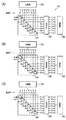
以下、TMEMからリードした複数のTMEM変数をシフト値に応じてローテイトする方法について説明する。すなわち、図5および図6に示すように、ブロックサイズ8の検査行列H4を用いた、TMEM132からリードした8個のTMEM変数の処理の場合には、誤り検出訂正回路101では、LMEM126と、TMEM126と、演算ユニット130と、ローテイター132と、が使用される。演算ユニット130は8個の演算回路ALU0〜ALU8からなり、8個の処理を並列処理することができる。なお、ブロックサイズ8の検査行列H3を用いた場合のシフト値は、0〜7の8種類である。
Hereinafter, a method of rotating a plurality of TMEM variables read from TMEM in accordance with the shift value will be described. That is, as shown in FIGS. 5 and 6, in the case of processing of eight TMEM variables read from the
図5(A)および図6(A)に示すように、シフト値が「0」のブロックB(0)場合は、ローテイター132によりローテイト値0のローテイト処理が行われ、同一アドレスの変数同士で演算が実行される。ただし、ローテイト値0のローテイト処理とはローテイトされないことである。
As shown in FIG. 5A and FIG. 6A, in the case of block B (0) with a shift value of “0”, rotation processing with a rotation value of 0 is performed by the
列アドレス0のLMEM変数、行アドレス0のTMEM変数(図5(A)破線表示)
列アドレス1のLMEM変数、行アドレス1のTMEM変数
列アドレス2のLMEM変数、行アドレス2のTMEM変数
・
・
列アドレス7のLMEM変数、行アドレス7のTMEM変数(図5(A)破線表示)
LMEM variable at
LMEM variable at
・
・
LMEM variable at
これに対して、図5(B)および図6(B)に示すように、シフト値が「1」のブロックB(1)の場合は、ローテイター132によりローテイト値1のローテイト処理が行われ、以下のような変数同士で演算が実行される。すなわち、ローテイト値1のローテイト処理とは、それぞれの変数をひとつ下段に移動し、あふれた最下段の変数を最上段に挿入するシフト処理である。
On the other hand, as shown in FIGS. 5B and 6B, in the case of the block B (1) with the shift value “1”, the rotation process of the rotate
列アドレス0のLMEM変数、行アドレス7のTMEM変数(図5(B)破線表示)
列アドレス1のLMEM変数、行アドレス0のTMEM変数(図5(B)破線表示)
列アドレス2のLMEM変数、行アドレス1のTMEM変数
・
・
列アドレス7のLMEM変数、行アドレス6のTMEM変数
LMEM variable at
LMEM variable at
LMEM variable at
・
・
LMEM variable at
そして、図6(C)に示すように、シフト値が「7」のブロックB(7)の場合は、ローテイター132によりローテイト値7のローテイト処理が行われ、以下のような変数同士で演算が実行される。すなわち、ローテイト値7のローテイト処理とは、ローテイト値1のローテイト処理を7回行う処理である。
As shown in FIG. 6C, in the case of the block B (7) with the shift value “7”, the rotation process of the rotate
列アドレス0のLMEM変数、行アドレス1のTMEM変数
列アドレス1のLMEM変数、行アドレス2のTMEM変数
列アドレス2のLMEM変数、行アドレス3のTMEM変数
・
・
列アドレス7のLMEM変数、行アドレス0のTMEM変数
LMEM variable at
・
・
LMEM variable at
図7に、ブロックシフト値(0〜7)毎の演算回路入力変数の組み合わせを示す。 FIG. 7 shows combinations of arithmetic circuit input variables for each block shift value (0 to 7).
以上のように、ローテイター132は、LMEM126あるいはTMEM132からリードした変数を演算ユニット130に入力する前にブロックのシフト値に応じたローテイト値にローテイトする。ブロックサイズ8の検査行列H3を用いた誤り検出訂正回路101の場合には、ローテイター132の最大ローテイト値は「ブロックサイズ−1」の「7」になる。信頼度の量子化ビット数を「u」とすると、それぞれの変数のビット数は「u」になるので、ローテイター132の入出力データ幅は「8×u」ビットになる。
As described above, the
<第1の実施の形態>
以下、本発明の第1の実施の形態の誤り検出訂正回路、メモリコントローラ、および半導体メモリ装置(以下、「誤り検出訂正回路等」ともいう」について説明する。
<First Embodiment>
Hereinafter, an error detection and correction circuit, a memory controller, and a semiconductor memory device (hereinafter also referred to as “error detection and correction circuit or the like”) according to the first embodiment of the present invention will be described.
以上の説明では、説明を簡単にするために、ブロックサイズ等が極端に小さい例(p=8等)について説明したが、例えば、半導体メモリ装置のメモリコントローラの誤り検出訂正回路では、ブロックサイズpは、128〜256規模の値になり、非常に大きい。このため、第1の実施の形態の誤り検出訂正回路では、ブロックサイズのp個、設置する必要のある演算回路ALUを、1/Y(Yは2以上の整数)に削減して並列度を意図的に下げている。なお、以下の説明では、やはり説明を簡単にするために、ブロックサイズ等が小さく(p=8)、Y=2の場合を例に説明する。 In the above description, in order to simplify the description, an example in which the block size or the like is extremely small (p = 8 or the like) has been described. For example, in the error detection and correction circuit of the memory controller of the semiconductor memory device, the block size p Is a value of 128 to 256 and is very large. For this reason, in the error detection and correction circuit according to the first embodiment, the number of arithmetic circuits ALU that need to be installed, which is p blocks, is reduced to 1 / Y (Y is an integer of 2 or more), and the degree of parallelism is reduced. Intentionally lowered. In the following description, in order to simplify the description, a case where the block size or the like is small (p = 8) and Y = 2 will be described as an example.
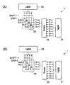
最初に、図9を用いて本発明の第1の実施の形態の誤り検出訂正回路1、誤り検出訂正回路1を有するメモリコントローラ2および誤り検出訂正回路1を有する半導体メモリ装置であるメモリカード3の構成を説明する。
First, referring to FIG. 9, the error detection and
図9に示すように、メモリカード3はパソコンまたはデジタルカメラ等のホスト4から受信したデータを記憶し、記憶したデータをホスト4に送信する記憶媒体である。メモリカード3は、半導体メモリ部(以下、単に「メモリ部」ともいう。)13と、誤り検出訂正回路1を具備したメモリコントローラ2とを有する。メモリ部13は、NAND型フラッシュメモリから構成されており、単位セルである多数のメモリセル13Dが、ビット線13E等で接続された構造を有する。
As shown in FIG. 9, the
そして、メモリコントローラ2は、バス17を介して接続された、ROM10と、CPUコア11と、RAM18と、ホスト I/F(インターフェイス)14と、誤り訂正(ECC:Error Correcting Code)部15と、NAND I/F(インターフェイス)16とを有する。
The
メモリコントローラ2は、CPUコア11を用いて、ホスト I/F14を介してホスト4とのデータ送受信を、NAND I/F16を介してメモリ部13とのデータ送受信を行う。またメモリコントローラ2は、書き換え回数の制限を含めたメモリ部13のアドレス管理をCPUコア11で実行されるFW(Firm Ware)で実現している。また、ホスト4からのコマンド入力に応じたメモリカード3全体の制御もFWで実行される。ROM10には、メモリカード3の制御プログラム等が記憶されており、RAM18には、アドレス管理で必要となるアドレス変換デーブル等が記憶される。
The
ECC部15は、データ記憶時に誤り訂正符号を生成し付与する符号化器12と、データ読み出し時に、読み出された符号化データを復号する誤り検出訂正回路1とを有する。本実施の形態のECC部15は、確率にもとづく反復計算により復号処理される誤り訂正符号であるLDPC符号を用いる。
The
そして、図10に示すように、誤り検出訂正回路1は、制御部20と、受信部21と、初期LLR算出部22と、硬判定部24と、パリティ検査部25と、第1のメモリであるビットノード記憶部(LMEM)26と、ローテイター32と、第2のメモリであるチェックノード記憶部(TMEM)31と、演算ユニット30と、第1のセレクタであるセレクタ23と、第2のセレクタであるセレクタ36と、を有する。制御部20は誤り検出訂正回路1全体の制御を行うが、CPUコア11の一部であってもよい。受信部21は、バス17を介してメモリ部13に記憶されていた符号化データを受信する。ここで、符号化データは、例えば、NAND型フラッシュメモリの読み出し電圧として誤り検出訂正回路1に入力される。初期LLR算出部22は入力された符号化データをもとに図示しない対数尤度比テーブル等を用いて初期LLRを算出する。硬判定部24は、事後確率(LLR)をもとに、ビットデータが「0」または「1」のいずれか硬判定する。
As shown in FIG. 10, the error detection and
パリティ検査部25は、硬判定されたデータのパリティ検査を行う。セレクタ23は、制御部20の制御によりデータを、検査行列のブロックサイズpにあわせたp(8)個のグループ単位にデータを分割する。セレクタ35、36は、制御部20の制御によりそれぞれのグループから、1/Y(1/2)のサイズのp/Y(4)個のサブグループを選択し分割する。すなわち、それぞれの分割処理はセレクタ23、35、36が所定のデータのみを選択することにより行われる。ビットノード記憶部(LMEM)26はビットノード単位での事前/事後確率βを求めるための第1の変数であるLMEM変数を格納する。チェックノード記憶部(TMEM)はチェックノード単位で外部値αを求めるための第2の変数であるTMEM変数を格納する。ローテイター32は制御部20の制御により、TMEM変数を所定のローテイト値にローテイト処理する。演算ユニット30は、チェックノード演算部29と、ビットノード演算部28とを有する。
The
次に、図10〜図14を用いて、本実施の形態の誤り検出訂正回路1の動作の流れについて説明する。
Next, the operation flow of the error detection /
<ステップS10> データ受信
受信部21は、メモリ部13に記憶されていた符号化データを受信する。
<Step S10> Data reception
The receiving
<ステップS11> 初期LLR値受信
初期LLR算出部22が、尤度比テーブル(不図示)等をもとに符号化データから初期LLR(事前確率β)を算出する。
<Step S11> Initial LLR Value Reception The initial
<ステップS12> 硬判定
LLRをもとに、硬判定が行われ、一時推定語が生成される。
<Step S12> Hard decision Based on the LLR, a hard decision is made and a temporary estimated word is generated.
<ステップS13> パリティチェック
パリティ検査部25は、一時推定語を用いてパリティチェックを行う。
<Step S13> Parity check
The
<ステップS14> パリティチェックOK?
パリティ検査部25は、パリティチェックの結果、誤りがないことが確認された場合(Yes)には、ステップS15において、復号データをホストI/F14を介してホスト4に出力し、処理は終了する。
<Step S14> Parity check OK?
If it is confirmed as a result of the parity check that there is no error (Yes), the
<ステップS16> 初期化/分割
パリティ検査部25は、パリティチェックの結果、誤りがあった場合(S14:No)には、イタレーション処理を開始するために、ブロックのシフト値を初期化する。また、制御部20は、セレクタ23により、事前確率βとなる初期LLRのデータをp(8)個単位のグループに分割し、グループ単位で以下の処理を行う。
<Step S16> Initialization / Division When there is an error as a result of the parity check (S14: No), the
<ステップS17> 事前確率β格納
所定のグループの事前確率β(LMEM変数)が、LMEM26に送信され、第1のアドレスであるLMEMアドレスと関連付けて格納される。
<Step S17> Prior Probability β Storage A predetermined group prior probability β (LMEM variable) is transmitted to the
<ステップS18>サブグループ分割
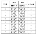
LMEM26に格納されたLMEM変数は、セレクタ36によりY(2)個のサブグループに分割され、順にS19からの処理が行われる。ここで、サブグループは、LMEMアドレスにもとづいて、例えば、アドレス中央値を基準に、上位アドレスサブグループと下位アドレスサブグループとに分割される。後に説明するようにTMEM変数も、セレクタ35によりY(2)個のサブグループに分割され処理される。例えば、LMEM変数、TMEM変数は、アドレスが(0、1、2、3)のサブグループLA、TAと、アドレスが(4、5、6、7)のサブグループLB、TBと、に分割される。
<Step S18> Subgroup Division The LMEM variable stored in the
<ステップS19>チェックノード処理(行処理)/ビットノード処理(列処理)
ビットノードから接続されているチェックノードに事前確率βが送信され、チェックノード演算部29は、受信した確率の積を算出し接続されているビットノードに外部情報αとして送信する。外部情報αはTMEM31に第2のアドレスであるTMEMアドレスと関連付けて格納される。
<Step S19> Check node processing (row processing) / bit node processing (column processing)
The prior probability β is transmitted from the bit node to the connected check node, and the check
チェックノードでは、接続されているビットノードに外部情報αが送信され、ビットノード演算部28は受信した確率の積を算出し接続されているチェックノードに、事後確率βとして送信する。事後確率βはLMEM26に、第1のアドレスであるLMEMアドレスと関連付けて格納される。なおTMEM31、LMEM26に、既に格納されている変数がある場合には、新しい変数が上書きされる。
In the check node, the external information α is transmitted to the connected bit node, and the bit
このとき、図11〜図14に示すように、シフト値が偶数の場合、ステップ1にてサブグループLA(変数アドレス0〜3)、サブグループTA(変数アドレス0〜3)をアクセスし、ステップ2にてサブグループLB(変数アドレス4〜7)、サブグループTB(変数アドレス4〜7)をアクセスし、シフト値が奇数の場合、ステップ1にてサブグループLA(変数アドレス0〜3)、サブグループTB(変数アドレス4〜7)をアクセスし、ステップ2にてサブグループLB(変数アドレス4〜7)、サブグループTA(変数アドレス0〜3)をアクセスする。ここで、サブグループにアクセスするとは、演算ユニット30がアクセスされた2つの変数を用いて演算処理を行うことを意味する。
すなわち、並列処理毎に、TMEM31に格納されていたTMEM変数は、シフト値とローテイト値とに応じたローテイト処理がローテイター32により行われ、セレクタ35、36により演算に必要なサブグループの変数が選択される。
At this time, as shown in FIGS. 11 to 14, when the shift value is an even number, the subgroup LA (variable addresses 0 to 3) and the subgroup TA (variable addresses 0 to 3) are accessed in
That is, for each parallel process, the TMEM variable stored in the
なお、図14等において、ローテイト値4(0)とは、ローテイト処理により、並び順が1周して再び「0」になったという意味である。 In FIG. 14 and the like, the rotate value 4 (0) means that the order of rotation is one round and again becomes “0” by the rotate process.
<ステップS20〜S23>
全てのサブグループ(ステップ:ローテイト値)/グループ(シフト値)の処理が完了するまで、行処理/列処理が行われる。すなわち、p=8、Y=2の場合には、ステップS18〜S23の処理が8回行われ、さらに、それぞれの繰り返し処理の中でステップS19〜S21の処理が2回行われる。
<Steps S20 to S23>
Row processing / column processing is performed until processing of all subgroups (step: rotate value) / group (shift value) is completed. That is, when p = 8 and Y = 2, the processes of steps S18 to S23 are performed eight times, and further, the processes of steps S19 to S21 are performed twice in each repetitive process.
1ラウンドの処理が完了すると、ステップS12において硬判定処理が行われ、さらにステップS13においてパリティチェックが行われ、OKの場合には処理は完了する。NGの場合には、ステップS17からの処理が繰り返し行われる。 When the process of one round is completed, a hard decision process is performed in step S12, a parity check is further performed in step S13, and if OK, the process is completed. In the case of NG, the processing from step S17 is repeated.
以上で説明した誤り検出訂正回路1は、演算ユニット30の演算回路ALUの数をp(8)個から1/Y(1/2)の、p/Y(4)個に低減できる。すなわち、回路規模が小さく、消費電力が低減した処理効率のよい誤り検出訂正回路である。また、誤り検出訂正回路1を有するメモリコントローラ2、および誤り検出訂正回路1を有する半導体メモリ装置であるメモリカード3は処理効率がよい。
The error detection and
なお、ブロックサイズpが64以上のときに、上記実施の形態の誤り検出訂正回路1の効果が明瞭となり、256以上のとき、さらに顕著となる。pの上限は実装の制限から決定されるが、例えば1k程度である。
When the block size p is 64 or more, the effect of the error detection /
以上の説明のように、本実施の形態の誤り検出訂正回路1は、低密度パリティ検査符号の検査行列のタナーグラフに対応して設定された複数の検査ノードおよび複数のビットノードの間で外部値α、確率βを反復伝搬させ、その過程において確率βから算出される事後値(事後確率:LLR)の硬判定値を検査行列でパリティ検査することにより収束判定し受信データの推定値を決定するサムプロダクト・アルゴリズムを用いて、受信データからの符号検出を行い、サイズp(pは8以上の整数)の単位行列からなるブロックと、前記単位行列の各行が「1」から「p−1」のシフト値に対応してシフトしている複数のブロックと、からなる前記検査行列をもとに、前記受信データを、p個のグループに分割する第1のセレクタと、それぞれの前記グループを、さらにY個(Yは2以上の整数)のサブグループに分割する第2のセレクタと、確率βを算出処理するための複数の第1の変数を、第1のアドレスと関連付けて格納する第1のメモリと、外部値αを算出処理するための複数の第2の変数を、第2のアドレスと関連付けて格納する第2のメモリと、前記第2のメモリに格納された複数の前記第2の変数に対して、前記シフト値と前記サブグループとに応じたローテイト値のローテイト処理を行い、演算ユニットに送信するローテイターと、前記シフト値に連動して前記サブグループ単位で、前記第1の変数と前記第2の変数とを用いて並列演算処理を行う(p/Y)個の演算回路からなる前記演算ユニットと、前記シフト値およびローテイト値に応じて、前記第1のセレクタ、前記第2のセレクタ、前記演算ユニット、および前記ローテイターを制御する制御部と、を具備する。
As described above, the error detection /
<第2の実施の形態>
以下、図面を参照して本発明の第2の実施の形態の誤り検出訂正回路1A等について説明する。第2の実施の形態の誤り検出訂正回路1A等は、第1の実施の形態の誤り検出訂正回路1と類似しているので、同じ説明は省略する。
<Second Embodiment>
The error detection /
第1の実施の形態の誤り検出訂正回路1は、演算ユニット30の演算回路ALUの数を1/Yに低減した。しかし、ブロックのシフト値制御の都合で、ローテイターの最大ローテイト値は「ブロックサイズ−1」を維持する必要がある。
In the error detection and
すなわち、ここで、1回目のラウンドでTMEM変数T1〜T4をローテイターに入力し、2回目のラウンドでT5〜T8を入力するように制御する場合を考えてみる。ブロックのシフト値が「7」だった場合、例えばTMEM変数T1を、最大シフト値の7ローテイトする必要があるが(図6(B)参照)、ローテイターは最大で4しかローテイトできないため、要求機能を満足することができない。すなわち、演算回路数は4に半減できるが、これにあわせてローテイターのローテイト機能(回路規模)を半減することはできなかった。また、ローテイター32に入力するTMEM変数の数も、ブロックサイズ分の8個必要になるので、TMEM31のリードデータ幅は「8×u」ビットのままである。さらに、演算ユニット30に必要な4個のTMEM変数を入力するためには、「8uビット to 4uビット」のセレクタ36が必要になる。
That is, consider the case where the TMEM variables T1 to T4 are input to the rotator in the first round, and T5 to T8 are input in the second round. When the block shift value is “7”, for example, the TMEM variable T1 needs to be rotated by 7 of the maximum shift value (see FIG. 6B), but since the rotator can rotate only 4 at the maximum, the requested function Can not be satisfied. That is, the number of arithmetic circuits can be halved to 4, but the rotation function (circuit scale) of the rotator cannot be halved in accordance with this. Further, since the number of TMEM variables input to the
このため、ブロックサイズが256規模あり、u=6ビットの誤り検出訂正回路では、ローテイター単体で例えば50Kゲート規模に達し、データバス幅も256×6ビット=1536ビットと膨大になる。このため、TMEMリードデータ幅、ローテイター規模、セレクタ規模、および前記回路を接続するデータバス幅等を、演算ユニット削減数に比例させて削減することはできなかった。 For this reason, in the error detection and correction circuit having a block size of 256, u = 6 bits, the rotator alone reaches, for example, 50K gate scale, and the data bus width is enormous, 256 × 6 bits = 1536 bits. For this reason, the TMEM read data width, the rotator scale, the selector scale, the data bus width connecting the circuits, and the like cannot be reduced in proportion to the number of arithmetic unit reductions.
これに対して、本実施の形態の誤り検出訂正回路1Aでは、LMEM変数およびTMEM変数をアドレスの大小による分割ではなく、アドレスの下位ビットにもとづき分割する。例えば、例えば、アドレスの最下位1ビットにもとづいて、アドレスが偶数のサブグループ(0、2、4、6)Teと、アドレスが奇数のサブグループ(1、3、5、7)Toと、の、2グループに分割する。
On the other hand, in the error detection /
すなわち、アドレスが偶数とは、アドレスの最下位1ビットが「0」であることを意味し、アドレスが奇数とは、アドレスの最下位1ビットが「1」であるであることを意味している。 That is, an even address means that the least significant bit of the address is “0”, and an odd address means that the least significant bit of the address is “1”. Yes.
そして、誤り検出訂正回路1Aのイタレーション処理においては、シフト値が偶数の場合、ステップ1にてサブグループLe、サブグループTeをアクセスし、ステップ2にてサブグループLo、サブグループToをアクセスし、シフト値が奇数の場合、ステップ1にてサブグループLe、サブグループToをアクセスし、ステップ2にてLo、Teをアクセスする。
In the iteration process of the error detection /
すなわち、ブロック演算処理のステップ1でサブグループLeの処理を実行し、ステップ2でサブグループLoの処理を実行すると、ブロックシフト値が偶数の場合、ステップ1にてサブグループLeはサブグループTeと演算を実行し、ステップ2にてサブグループLoはサブグループToと演算を実行する。そしてブロックシフト値が奇数の場合、ステップ1にてサブグループLeはサブグループToと演算を実行し、ステップ2にてサブグループLoはサブグループTeと演算を実行する。よって、ブロックシフト値が偶数の場合、ステップ1にてサブグループLe、サブグループTeをアクセスし、ステップ2にてサブグループLo、サブグループToをアクセスする。そしてブロックシフト値が奇数の場合、ステップ1にてサブグループLe、サブグループToをアクセスし、ステップ2にてサブグループLo、サブグループTeをアクセスする。
That is, when the processing of the subgroup Le is executed in
すなわち、誤り検出訂正回路1Aでは、TMEM変数は下位ビットにもとづいてサブグループ分けされているために、ローテイター32Aには演算処理に必要なサブグループだけが入力する。
That is, in the error detection and
図15〜図17に、誤り検出訂正回路1Aの各シフト値/各ステップにおけるTMEM変数ローテイト値の関係を示す。また図17にシフト値、ステップ、ローテイト値のまとめを示す。
15 to 17 show the relationship between each shift value / TMEM variable rotate value in each step of the error detection /
誤り検出訂正回路1Aでは、演算ユニット30Aの演算回路数を、1/Y=1/2、に削減できるだけでなく、TMEM31Aへのアクセス単位(1ワード)のデータ幅を8uビットから4uビットと1/2、に削減できる。さらに、ローテイター32Aの最大ローテイト値および入出力データ幅、TMEM31Aとローテイター32Aと演算ユニット30Aとを接続するデータバス幅、も1/2に削減できる。また、「8uビット to 4uビット」のセレクタ36は不要となる。
In the error detection and
すなわち、誤り検出訂正回路1Aは、第1の実施の形態の誤り訂正部1が有する効果に加えてローテイターを含む周辺メモリ、回路、およびデータバスの幅を、演算回路数に合わせて削減できる。すなわち、誤り検出訂正回路1Aは、柔軟に処理速度と回路規模/消費電力の調整が可能なスケーラビリティを備える。
That is, the error detection /
以上の説明のように、本実施の形態の誤り検出訂正回路1Aでは、制御部20が、第1のアドレスおよび第2のアドレスの最下位アドレス1ビットをもとに、各グループを2個のサブグループに分割するように制御する。
As described above, in the error detection /
また、誤り検出訂正回路1Aは、LDPC符号による誤り検出/訂正処理機能を備え、1ラウンドの処理(ラウンド処理)で、選択したビットノードに関して、LDPC符号のパリティ検査行列のタナーグラフに対応して設定された複数のチェックノードから当該チェックノードに接続されている複数のビットノードに向け外部情報(α)を伝搬する行処理、および、当該複数のビットノードから該複数のチェックノードに向け事後確率(β)を伝搬する列処理を連続実行する。そして、ラウンド処理繰り返しの過程において、βから算出される事後値を用いて収束判定し符号データの推定し、入力値からの符号検出を行う。そして、サイズp×p(pは8以上の整数)の正方行列を複数個組み合わせて検査行列を構成するもので、ビットノード単位での事前/事後確率βを求めるための変数を格納/管理するメモリ(LMEM)と、チェックノード単位で外部値αを求めるための変数を格納/管理するメモリ(TMEM)を備え、ブロックのシフト値に連動してp個のビットノードと、p個のチェックノード単位で演算処理する機能を備えるもので、p個のビットノードとチェックノードをp/Y個(Yは2以上の整数)のサブグループに分け、サブグループに対応する変数グループ単位で、LMEM/TMEMアクセスとアクセスした変数のローテーション処理を実行するもので、LMEM/TMEMの下位アドレスでサブグループ分けをする。
Further, the error detection /
さらに、誤り検出訂正回路1Aは、演算処理を実行するとき、LMEM、TMEMいずれかのワードアクセス順とローテイターのローテイト値を、ブロックシフト値に応じて、決定する機能を備えることが好ましく、特に好ましくは演算処理を実行するとき、TMEMのワードアクセス順とローテイターのローテイト値を、ブロックシフト値に応じて、決定する機能を備える。
Further, the error detection /
<第3の実施の形態>
以下、図面を参照して本発明の第3の実施の形態の誤り検出訂正回路1B等について説明する。第3の実施の形態の誤り検出訂正回路1B等は、第2の実施の形態の誤り検出訂正回路1Aと類似しているので、同じ説明は省略する。
<Third Embodiment>
The error detection /
本実施の形態の誤り検出訂正回路1Bは、サブグループ分割数Y=4の場合であり、演算ユニット30Bは、2(8/4)個の演算回路ALUを有している。すなわち、LMEM26B、TMEM31Bに格納された変数のアドレス最下位2ビットが「00」、「01」、「10」、「11」のいずれであるかに、もとづいて、LMEM変数およびTMEM変数を、それぞれ4つのサブグループに分割して、処理する。
The error detection and
誤り検出訂正回路1Bでは、第2の実施の形態の誤り検出訂正回路1A(Y=2)と同様に、制御部20がシフト値毎に、LMEM26B、TMEM31Bからアクセスする変数グループを、ローテイト値に応じてローテイター32Bがローテイト処理する。すなわち、制御部20が、ステップに応じてTMEM変数のローテイト値を制御する。図22に誤り検出訂正回路1Bにおけるシフト値、ステップ毎、ローテイト値のまとめを示す。
In the error detection /
誤り検出訂正回路1Bは、誤り検出訂正回路1Aが有する効果に加えて、より回路規模/消費電力を低減できる。なお、サブグループ分割数Yの上限は、処理速度と回路規模/消費電力とのトレードオフの関係から適宜、決定されるが、ブロックサイズp以下であり例えば8である。
The error detection /
以上の説明のように、本実施の形態の誤り検出訂正回路1Bでは、制御部20が、第1のアドレスおよび第2のアドレスの下位アドレス2ビットをもとに、各グループを4個のサブグループに分割するように制御する。
As described above, in the error detection and
なお以上は、ホスト4と接続されるメモリカード3からなるメモリシステムを例に説明したが、メモリシステムとしては、ホスト4の内部に収納され、ホスト4の起動データ等を記憶する、いわゆるエンベデッドタイプのNAND型フラッシュメモリ装置等でもメモリカード3等と同じ効果を得ることができる。さらには、符号化データの復号を確率にもとづく反復計算により行う誤り検出訂正回路であれば、デジタルテレビ放送受信機等の誤り検出訂正回路でも半導体メモリシステムと同じ効果を得ることができる。また、誤り検出訂正回路としては専用の回路ではなく汎用CPUに読み込まれ動作するものであってもよい。
In the above description, the memory system including the
本発明の、さらに別の実施の形態によるLDPC符号による誤り検出訂正方法は、受信信号からLLRを算出するLLR算出工程と、前記LLRまたは確率βをもとに硬判定を行う硬判定工程と、硬判定結果をもとにパリティ検査を行うパリティ検査工程と、前記受信信号をp個のグループに分割するグループ分割工程と、それぞれの前記グループをY個のサブグループに分割するサブグループ分割工程と、前記確率βを算出処理するための前記サブグループの複数の第1の変数を、第1のアドレスと関連付けて第1のメモリに格納するとともに、外部値αを算出処理するための前記サブグループの複数の第2の変数を、第2のアドレスと関連付けて第2のメモリに格納する変数格納工程と、前記第1のメモリに格納された前記複数の第1の変数に対して選択処理する選択工程と、前記第2のメモリに格納された前記複数の第2の変数に対してローテイト処理するローテイト工程と、選択処理されたp/Y個の前記第1の変数とローテイト処理されたp/Y個の前記第2の変数とをp/Y個の演算回路により並列処理する並列処理工程と、を具備する。ただし前記LDPC符号はサイズp(pは8以上の整数)の単位行列からなるブロックと、前記単位行列の各行が「1」から「p−1」のシフト値に対応してシフトしている複数のブロックと、からなる検査行列をもとにし、前記グループは前記シフト値に対応しており、前記ローテイト処理および前記選択処理は、前記シフト値および前記サブグループに応じたローテイト値にもとづき実行される。 An error detection and correction method using an LDPC code according to still another embodiment of the present invention includes an LLR calculation step of calculating an LLR from a received signal, a hard decision step of performing a hard decision based on the LLR or the probability β, A parity check step for performing a parity check based on a hard decision result, a group division step for dividing the received signal into p groups, and a sub-group division step for dividing each of the groups into Y sub-groups. A plurality of first variables of the subgroup for calculating the probability β are stored in a first memory in association with a first address, and the subgroup for calculating the external value α A plurality of second variables stored in the second memory in association with the second address, and the plurality of first variables stored in the first memory. A selection process for performing a selection process for the plurality of second variables stored in the second memory, a rotation process for performing a rotation process on the plurality of second variables, and the p / Y first variables subjected to the selection process. And p / Y second variables that have been subjected to the rotation process, and a parallel processing step that performs parallel processing using p / Y arithmetic circuits. However, the LDPC code includes a block composed of a unit matrix of size p (p is an integer of 8 or more), and a plurality of rows in which each row of the unit matrix is shifted corresponding to a shift value from “1” to “p−1”. And the group corresponds to the shift value, and the rotation process and the selection process are performed based on the shift value and the rotate value corresponding to the subgroup. The
さらに、上記誤り検出訂正方法において、サブグループ分割工程は、前記第1のアドレスおよび前記第2のアドレスの下位アドレスをもとに行われることが好ましく、より好ましくは前記第1のアドレスおよび前記第2のアドレスの最下位アドレス1ビットをもとに行われる。
Further, in the error detection and correction method, the subgroup division step is preferably performed based on the lower address of the first address and the second address, more preferably, the first address and the second address. This is done based on the
上記のように、本発明は、上述した実施の形態に限定されるものではなく、本発明の要旨を変えない範囲において、種々の変更、改変等が可能である。 As described above, the present invention is not limited to the above-described embodiments, and various changes and modifications can be made without departing from the scope of the present invention.
1、1A、1B…誤り検出訂正回路、2…メモリコントローラ、3…メモリカード、4…ホスト、10…ROM、11…CPUコア、12…符号化器、13…メモリ部、13D…メモリセル、13E…ビット線、14…Host I/F、16…NAND I/F、17…バス、18…RAM、20…制御部、21…受信部、22…算出部、23…セレクタ、24…硬判定部、25…パリティ検査部、26、26A、26B…ビットノード記憶部(LMEM)、28…ビットノード演算部、29…チェックノード演算部、30、30A、30B…演算ユニット、31、31A、31B…チェックノード記憶部(TMEM)、32、32A、32B…ローテイター、35、36…セレクタ、101…誤り検出訂正回路、130…演算ユニット、132…ローテイター、ALU…演算回路
DESCRIPTION OF
Claims (5)
サイズp(pは8以上の整数)の単位行列からなるブロックと、前記単位行列の各行が「1」から「p−1」のシフト値に対応してシフトしている複数のブロックと、からなる検査行列をもとに、前記受信データを、p個のデータからなるグループに分割し出力する第1のセレクタと、
それぞれの前記グループを、さらにY個(Yは2以上の整数)のサブグループに分割し出力する第2のセレクタと、
確率βを算出処理するための複数の第1の変数を、第1のアドレスと関連付けて格納する第1のメモリと、
外部値αを算出処理するための複数の第2の変数を、第2のアドレスと関連付けて格納する第2のメモリと、
前記第2のメモリに格納された前記複数の第2の変数に対して、前記シフト値と前記サブグループとに応じたローテイト値のローテイト処理を行い、演算ユニットに送信するローテイターと、
前記シフト値に連動して前記サブグループ単位で、前記第1の変数と前記第2の変数とを用いた並列演算処理を行う(p/Y)個の演算回路からなる前記演算ユニットと、
前記シフト値およびローテイト値に応じて、前記第1のセレクタ、前記第2のセレクタ、および前記ローテイターを制御する制御部と、を具備する。 An error detection and correction circuit that decodes received data encoded by a low density parity check code using a sum product algorithm,
A block composed of a unit matrix of size p (p is an integer of 8 or more), and a plurality of blocks in which each row of the unit matrix is shifted corresponding to a shift value from “1” to “p−1”. based on the check matrix comprising a first selector for the received data is divided into groups of p pieces of data output,
A second selector that divides and outputs each of the groups into Y (Y is an integer of 2 or more) subgroups;
A first memory for storing a plurality of first variables for calculating the probability β in association with the first address;
A second memory for storing a plurality of second variables for calculating the external value α in association with the second address;
A rotator that performs a rotation process of a rotate value according to the shift value and the subgroup on the plurality of second variables stored in the second memory, and transmits the rotate value to an arithmetic unit;
The arithmetic unit comprising (p / Y) arithmetic circuits that perform parallel arithmetic processing using the first variable and the second variable in units of the subgroup in conjunction with the shift value;
And a control unit for controlling the first selector, the second selector, and the rotator in accordance with the shift value and the rotate value.
Priority Applications (2)
| Application Number | Priority Date | Filing Date | Title |
|---|---|---|---|
| JP2010073411A JP5112468B2 (en) | 2010-03-26 | 2010-03-26 | Error detection and correction circuit, memory controller, and semiconductor memory device |
| US13/039,961 US8453034B2 (en) | 2010-03-26 | 2011-03-03 | Error detection/correction circuit, memory controller and semiconductor memory apparatus |
Applications Claiming Priority (1)
| Application Number | Priority Date | Filing Date | Title |
|---|---|---|---|
| JP2010073411A JP5112468B2 (en) | 2010-03-26 | 2010-03-26 | Error detection and correction circuit, memory controller, and semiconductor memory device |
Publications (2)
| Publication Number | Publication Date |
|---|---|
| JP2011205578A JP2011205578A (en) | 2011-10-13 |
| JP5112468B2 true JP5112468B2 (en) | 2013-01-09 |
Family
ID=44657753
Family Applications (1)
| Application Number | Title | Priority Date | Filing Date |
|---|---|---|---|
| JP2010073411A Expired - Fee Related JP5112468B2 (en) | 2010-03-26 | 2010-03-26 | Error detection and correction circuit, memory controller, and semiconductor memory device |
Country Status (2)
| Country | Link |
|---|---|
| US (1) | US8453034B2 (en) |
| JP (1) | JP5112468B2 (en) |
Families Citing this family (23)
| Publication number | Priority date | Publication date | Assignee | Title |
|---|---|---|---|---|
| CN102881324B (en) * | 2011-07-11 | 2015-07-08 | 澜起科技(上海)有限公司 | Write circuit, readout circuit, memory buffer and memory bank |
| CN102880567B (en) * | 2011-07-11 | 2016-02-10 | 澜起科技(上海)有限公司 | data read-write system |
| WO2013140727A1 (en) * | 2012-03-19 | 2013-09-26 | パナソニック株式会社 | Decoding device |
| JP5801231B2 (en) | 2012-03-22 | 2015-10-28 | 株式会社東芝 | Transmission system, decoding device, memory controller, and memory system |
| US9136011B2 (en) * | 2012-04-26 | 2015-09-15 | Hgst Technologies Santa Ana, Inc. | Soft information module |
| US8689076B2 (en) * | 2012-07-02 | 2014-04-01 | Lsi Corporation | Systems and methods for enhanced bit correlation usage |
| KR101926608B1 (en) * | 2012-08-27 | 2018-12-07 | 삼성전자 주식회사 | Hard decision decoding method and low density parity check decoder using method thereof |
| DE102012216763B4 (en) | 2012-09-19 | 2018-09-13 | Deutsches Zentrum für Luft- und Raumfahrt e.V. | Procedure for recovering lost and / or corrupted data |
| KR102104937B1 (en) | 2013-06-14 | 2020-04-27 | 삼성전자주식회사 | Method and apparatus for encoding and decoding of low density parity check codes |
| US9118446B2 (en) * | 2013-09-19 | 2015-08-25 | Huawei Technologies Co., Ltd. | Methods and user equipment in a wireless communication network |
| US20150254130A1 (en) * | 2013-12-03 | 2015-09-10 | Kabushiki Kaisha Toshiba | Error correction decoder |
| JP2015115905A (en) * | 2013-12-13 | 2015-06-22 | 日本放送協会 | Receiver |
| TWI530959B (en) | 2014-06-17 | 2016-04-21 | 慧榮科技股份有限公司 | Method for controlling a memory apparatus, and associated memory apparatus thereof and associated controller thereof |
| JP2016062463A (en) * | 2014-09-19 | 2016-04-25 | 株式会社東芝 | Memory system, error correction unit and error correction method |
| KR102287625B1 (en) * | 2015-02-16 | 2021-08-10 | 한국전자통신연구원 | Bit interleaver for 4096-symbol mapping and low density parity check codeword with 64800 length, 2/15 rate, and method using the same |
| KR102287623B1 (en) * | 2015-02-16 | 2021-08-10 | 한국전자통신연구원 | Bit interleaver for 1024-symbol mapping and low density parity check codeword with 64800 length, 4/15 rate, and method using the same |
| US20160378591A1 (en) | 2015-06-24 | 2016-12-29 | Intel Corporation | Adaptive error correction in memory devices |
| WO2017084024A1 (en) * | 2015-11-17 | 2017-05-26 | 华为技术有限公司 | Decoding method and decoder for low-density parity check code |
| KR102466325B1 (en) * | 2015-12-14 | 2022-11-15 | 삼성전자주식회사 | Generating method for low density parity check code and generating circuit for low density parity check code |
| CN107124187B (en) * | 2017-05-05 | 2020-08-11 | 南京大学 | LDPC code decoder based on equal-difference check matrix and applied to flash memory |
| WO2019003888A1 (en) * | 2017-06-26 | 2019-01-03 | ソニーセミコンダクタソリューションズ株式会社 | Information processing device and method |
| CN112821889B (en) * | 2019-11-15 | 2024-02-20 | 京东方科技集团股份有限公司 | Output control circuit, data transmission method and electronic equipment |
| JP2022029558A (en) * | 2020-08-05 | 2022-02-18 | 株式会社東芝 | Magnetic disc apparatus and error correction method |
Family Cites Families (9)
| Publication number | Priority date | Publication date | Assignee | Title |
|---|---|---|---|---|
| US7072417B1 (en) * | 2000-06-28 | 2006-07-04 | Marvell International Ltd. | LDPC encoder and method thereof |
| US6633856B2 (en) * | 2001-06-15 | 2003-10-14 | Flarion Technologies, Inc. | Methods and apparatus for decoding LDPC codes |
| US7178080B2 (en) * | 2002-08-15 | 2007-02-13 | Texas Instruments Incorporated | Hardware-efficient low density parity check code for digital communications |
| US7162684B2 (en) * | 2003-01-27 | 2007-01-09 | Texas Instruments Incorporated | Efficient encoder for low-density-parity-check codes |
| US7401283B2 (en) | 2004-09-28 | 2008-07-15 | Broadcom Corporation | Amplifying magnitude metric of received signals during iterative decoding of LDPC (Low Density Parity Check) code and LDPC coded modulation |
| US20080104474A1 (en) * | 2004-10-01 | 2008-05-01 | Joseph J Laks | Low Density Parity Check (Ldpc) Decoder |
| US8181083B2 (en) * | 2007-08-27 | 2012-05-15 | Stmicroelectronics S.R.L. | Methods and architectures for layered decoding of LDPC codes with minimum latency |
| JP2009260692A (en) * | 2008-04-17 | 2009-11-05 | Pioneer Electronic Corp | Decoding apparatus and decoding method |
| JP2009271852A (en) * | 2008-05-09 | 2009-11-19 | Toshiba Corp | Semiconductor storage device |
-
2010
- 2010-03-26 JP JP2010073411A patent/JP5112468B2/en not_active Expired - Fee Related
-
2011
- 2011-03-03 US US13/039,961 patent/US8453034B2/en not_active Expired - Fee Related
Also Published As
| Publication number | Publication date |
|---|---|
| JP2011205578A (en) | 2011-10-13 |
| US20110239080A1 (en) | 2011-09-29 |
| US8453034B2 (en) | 2013-05-28 |
Similar Documents
| Publication | Publication Date | Title |
|---|---|---|
| JP5112468B2 (en) | Error detection and correction circuit, memory controller, and semiconductor memory device | |
| US8782496B2 (en) | Memory controller, semiconductor memory apparatus and decoding method | |
| JP7372369B2 (en) | Structural LDPC encoding, decoding method and device | |
| KR101789959B1 (en) | Encoding Method, Decoding Method, Encoding device and Decoding Device for Structured LDPC | |
| US9996420B2 (en) | Error-correction encoding and decoding | |
| Esfahanizadeh et al. | Finite-length construction of high performance spatially-coupled codes via optimized partitioning and lifting | |
| KR101944526B1 (en) | Transmitting apparatus and interleaving method thereof | |
| US8572463B2 (en) | Quasi-cyclic LDPC encoding and decoding for non-integer multiples of circulant size | |
| US9195536B2 (en) | Error correction decoder and error correction decoding method | |
| US20150227419A1 (en) | Error correction decoder based on log-likelihood ratio data | |
| CN107852176A (en) | LDPC code encoder and decoder | |
| JPWO2010073922A1 (en) | Error correction encoding apparatus, decoding apparatus, encoding method, decoding method, and program thereof | |
| KR102098202B1 (en) | Encoding apparatus and encoding method thereof | |
| WO2017113507A1 (en) | Set decoding method and set decoder | |
| KR102019893B1 (en) | Apparatus and method for receiving signal in communication system supporting low density parity check code | |
| US8448041B1 (en) | Multistage LDPC encoding | |
| US20140281794A1 (en) | Error correction circuit | |
| US20120054580A1 (en) | Error detection correction method and semiconductor memory apparatus | |
| CN114499541A (en) | Layered decoding method, device, terminal equipment and medium | |
| US11190220B2 (en) | Apparatus and method for managing parity check matrix | |
| US11075650B1 (en) | Sub-matrix reduction for quasi-cyclic LDPC codes | |
| US20150254130A1 (en) | Error correction decoder | |
| CN108809327B (en) | LDPC decoding method | |
| EP3496277A1 (en) | Parallel encoding method and system for protograph-based ldpc codes with hierarchical lifting stages | |
| JP2006100941A (en) | Signal processing apparatus, and coding method and decoding method of low density parity check code |
Legal Events
| Date | Code | Title | Description |
|---|---|---|---|
| A621 | Written request for application examination |
Free format text: JAPANESE INTERMEDIATE CODE: A621 Effective date: 20120208 |
|
| A977 | Report on retrieval |
Free format text: JAPANESE INTERMEDIATE CODE: A971007 Effective date: 20120528 |
|
| A131 | Notification of reasons for refusal |
Free format text: JAPANESE INTERMEDIATE CODE: A131 Effective date: 20120612 |
|
| A521 | Request for written amendment filed |
Free format text: JAPANESE INTERMEDIATE CODE: A523 Effective date: 20120810 |
|
| TRDD | Decision of grant or rejection written | ||
| A01 | Written decision to grant a patent or to grant a registration (utility model) |
Free format text: JAPANESE INTERMEDIATE CODE: A01 Effective date: 20120911 |
|
| A01 | Written decision to grant a patent or to grant a registration (utility model) |
Free format text: JAPANESE INTERMEDIATE CODE: A01 |
|
| A61 | First payment of annual fees (during grant procedure) |
Free format text: JAPANESE INTERMEDIATE CODE: A61 Effective date: 20121010 |
|
| FPAY | Renewal fee payment (event date is renewal date of database) |
Free format text: PAYMENT UNTIL: 20151019 Year of fee payment: 3 |
|
| FPAY | Renewal fee payment (event date is renewal date of database) |
Free format text: PAYMENT UNTIL: 20151019 Year of fee payment: 3 |
|
| LAPS | Cancellation because of no payment of annual fees |