JP5108381B2 - Bonding method, bonding apparatus, semiconductor device manufacturing method, and semiconductor device manufacturing apparatus - Google Patents
Bonding method, bonding apparatus, semiconductor device manufacturing method, and semiconductor device manufacturing apparatus Download PDFInfo
- Publication number
- JP5108381B2 JP5108381B2 JP2007136213A JP2007136213A JP5108381B2 JP 5108381 B2 JP5108381 B2 JP 5108381B2 JP 2007136213 A JP2007136213 A JP 2007136213A JP 2007136213 A JP2007136213 A JP 2007136213A JP 5108381 B2 JP5108381 B2 JP 5108381B2
- Authority
- JP
- Japan
- Prior art keywords
- flexible substrate
- row
- semiconductor integrated
- antennas
- integrated circuits
- Prior art date
- Legal status (The legal status is an assumption and is not a legal conclusion. Google has not performed a legal analysis and makes no representation as to the accuracy of the status listed.)
- Expired - Fee Related
Links
Images


Classifications
-
- H—ELECTRICITY
- H01—ELECTRIC ELEMENTS
- H01L—SEMICONDUCTOR DEVICES NOT COVERED BY CLASS H10
- H01L2221/00—Processes or apparatus adapted for the manufacture or treatment of semiconductor or solid state devices or of parts thereof covered by H01L21/00
- H01L2221/67—Apparatus for handling semiconductor or electric solid state devices during manufacture or treatment thereof; Apparatus for handling wafers during manufacture or treatment of semiconductor or electric solid state devices or components; Apparatus not specifically provided for elsewhere
- H01L2221/683—Apparatus for handling semiconductor or electric solid state devices during manufacture or treatment thereof; Apparatus for handling wafers during manufacture or treatment of semiconductor or electric solid state devices or components; Apparatus not specifically provided for elsewhere for supporting or gripping
- H01L2221/68304—Apparatus for handling semiconductor or electric solid state devices during manufacture or treatment thereof; Apparatus for handling wafers during manufacture or treatment of semiconductor or electric solid state devices or components; Apparatus not specifically provided for elsewhere for supporting or gripping using temporarily an auxiliary support
- H01L2221/68359—Apparatus for handling semiconductor or electric solid state devices during manufacture or treatment thereof; Apparatus for handling wafers during manufacture or treatment of semiconductor or electric solid state devices or components; Apparatus not specifically provided for elsewhere for supporting or gripping using temporarily an auxiliary support used as a support during manufacture of interconnect decals or build up layers
-
- H—ELECTRICITY
- H01—ELECTRIC ELEMENTS
- H01L—SEMICONDUCTOR DEVICES NOT COVERED BY CLASS H10
- H01L2224/00—Indexing scheme for arrangements for connecting or disconnecting semiconductor or solid-state bodies and methods related thereto as covered by H01L24/00
- H01L2224/01—Means for bonding being attached to, or being formed on, the surface to be connected, e.g. chip-to-package, die-attach, "first-level" interconnects; Manufacturing methods related thereto
- H01L2224/10—Bump connectors; Manufacturing methods related thereto
- H01L2224/15—Structure, shape, material or disposition of the bump connectors after the connecting process
- H01L2224/16—Structure, shape, material or disposition of the bump connectors after the connecting process of an individual bump connector
-
- H—ELECTRICITY
- H01—ELECTRIC ELEMENTS
- H01L—SEMICONDUCTOR DEVICES NOT COVERED BY CLASS H10
- H01L2924/00—Indexing scheme for arrangements or methods for connecting or disconnecting semiconductor or solid-state bodies as covered by H01L24/00
- H01L2924/01—Chemical elements
- H01L2924/01046—Palladium [Pd]
-
- H—ELECTRICITY
- H01—ELECTRIC ELEMENTS
- H01L—SEMICONDUCTOR DEVICES NOT COVERED BY CLASS H10
- H01L2924/00—Indexing scheme for arrangements or methods for connecting or disconnecting semiconductor or solid-state bodies as covered by H01L24/00
- H01L2924/01—Chemical elements
- H01L2924/01067—Holmium [Ho]
-
- H—ELECTRICITY
- H01—ELECTRIC ELEMENTS
- H01L—SEMICONDUCTOR DEVICES NOT COVERED BY CLASS H10
- H01L2924/00—Indexing scheme for arrangements or methods for connecting or disconnecting semiconductor or solid-state bodies as covered by H01L24/00
- H01L2924/01—Chemical elements
- H01L2924/01068—Erbium [Er]
-
- H—ELECTRICITY
- H01—ELECTRIC ELEMENTS
- H01L—SEMICONDUCTOR DEVICES NOT COVERED BY CLASS H10
- H01L2924/00—Indexing scheme for arrangements or methods for connecting or disconnecting semiconductor or solid-state bodies as covered by H01L24/00
- H01L2924/01—Chemical elements
- H01L2924/01077—Iridium [Ir]
-
- H—ELECTRICITY
- H01—ELECTRIC ELEMENTS
- H01L—SEMICONDUCTOR DEVICES NOT COVERED BY CLASS H10
- H01L2924/00—Indexing scheme for arrangements or methods for connecting or disconnecting semiconductor or solid-state bodies as covered by H01L24/00
- H01L2924/10—Details of semiconductor or other solid state devices to be connected
- H01L2924/102—Material of the semiconductor or solid state bodies
- H01L2924/1025—Semiconducting materials
- H01L2924/10251—Elemental semiconductors, i.e. Group IV
- H01L2924/10253—Silicon [Si]
-
- H—ELECTRICITY
- H01—ELECTRIC ELEMENTS
- H01L—SEMICONDUCTOR DEVICES NOT COVERED BY CLASS H10
- H01L2924/00—Indexing scheme for arrangements or methods for connecting or disconnecting semiconductor or solid-state bodies as covered by H01L24/00
- H01L2924/10—Details of semiconductor or other solid state devices to be connected
- H01L2924/11—Device type
- H01L2924/13—Discrete devices, e.g. 3 terminal devices
- H01L2924/1304—Transistor
- H01L2924/1306—Field-effect transistor [FET]
- H01L2924/13091—Metal-Oxide-Semiconductor Field-Effect Transistor [MOSFET]
-
- H—ELECTRICITY
- H01—ELECTRIC ELEMENTS
- H01L—SEMICONDUCTOR DEVICES NOT COVERED BY CLASS H10
- H01L2924/00—Indexing scheme for arrangements or methods for connecting or disconnecting semiconductor or solid-state bodies as covered by H01L24/00
- H01L2924/10—Details of semiconductor or other solid state devices to be connected
- H01L2924/146—Mixed devices
- H01L2924/1461—MEMS
Landscapes
- Credit Cards Or The Like (AREA)
Abstract
Description
本発明はフレキシブル(可撓性を有する)基板上に設けられた回路(または素子)に対して半導体集積回路を電気的に接続する半導体装置の作製方法に関する。特に、ロールtoロール方式を用いる半導体装置の作製方法に関する。フレキシブル基板上に形成されたアンテナに対して半導体集積回路を電気的に接続する半導体装置の作製方法に関する。アンテナを介した無線通信によりデータの入出力を行う半導体装置の作製方法に関する。また、半導体装置の製造装置に関する。 The present invention relates to a method for manufacturing a semiconductor device in which a semiconductor integrated circuit is electrically connected to a circuit (or an element) provided on a flexible substrate. In particular, the present invention relates to a method for manufacturing a semiconductor device using a roll-to-roll method. The present invention relates to a method for manufacturing a semiconductor device in which a semiconductor integrated circuit is electrically connected to an antenna formed over a flexible substrate. The present invention relates to a method for manufacturing a semiconductor device that inputs and outputs data by wireless communication via an antenna. The present invention also relates to a semiconductor device manufacturing apparatus.
アンテナと当該アンテナと電気的に接続された半導体集積回路とを有する半導体装置は、RFIDタグとして注目されている。RFIDタグは、ICタグ、IDタグ、トランスポンダ、ICチップ、IDチップとも呼ばれる。フレキシブル基板上に複数のアンテナを設け、当該複数のアンテナに対して1つずつ半導体集積回路を電気的に接続するRFIDタグの作製方法が提案されている(特許文献1参照)。 A semiconductor device including an antenna and a semiconductor integrated circuit electrically connected to the antenna has attracted attention as an RFID tag. The RFID tag is also called an IC tag, an ID tag, a transponder, an IC chip, or an ID chip. A method for manufacturing an RFID tag in which a plurality of antennas are provided over a flexible substrate and a semiconductor integrated circuit is electrically connected to the plurality of antennas one by one has been proposed (see Patent Document 1).
また、1枚の基板(以下、素子基板ともいう)に複数の半導体集積回路を形成し、複数の半導体集積回路を1つずつ取り出し、取り出した半導体集積回路を素子基板とは別の基板上に実装する方法が提案されている(特許文献2参照)。
第1のフレキシブル基板上に配列された半導体集積回路と、第2のフレキシブル基板上に配列されたアンテナとを再配列することなく直接接続させるとタクトタイムを短くすることができる。 If the semiconductor integrated circuits arranged on the first flexible substrate and the antenna arranged on the second flexible substrate are directly connected without rearranging, the tact time can be shortened.
しかしながら、コストを低減するため、複数の半導体集積回路は素子基板上に高集積化して形成するのが好ましい。また、半導体集積回路の面積も小さくすることが好ましい。一方、アンテナは所定の周波数の電磁波を受信するために所定の形状及び大きさとする必要がある。そのため、半導体集積回路及びアンテナの大きさが異なってしまい、配置密度が異なる。この場合、再配列せずに、フレキシブル基板上の複数のアンテナに素子基板上に形成された複数の半導体集積回路を同時に電気的に接続することはできなかった。 However, in order to reduce cost, it is preferable that the plurality of semiconductor integrated circuits be formed on the element substrate with high integration. It is also preferable to reduce the area of the semiconductor integrated circuit. On the other hand, the antenna needs to have a predetermined shape and size in order to receive an electromagnetic wave having a predetermined frequency. Therefore, the sizes of the semiconductor integrated circuit and the antenna are different, and the arrangement density is different. In this case, a plurality of semiconductor integrated circuits formed on the element substrate cannot be simultaneously electrically connected to a plurality of antennas on the flexible substrate without rearrangement.
そのため、例えば特許文献2に記載されたような方法を用いて、素子基板上に形成された複数の半導体集積回路のうちの1つを取り出し、フレキシブル基板上の複数のアンテナのうち1つのアンテナに、接続する動作を、素子基板上に形成された全ての半導体集積回路に対して繰り返さなければならなかった。それ故、タクトタイムが長く、半導体装置の製造コストを高くしていた。 Therefore, for example, using a method as described in Patent Document 2, one of a plurality of semiconductor integrated circuits formed on the element substrate is taken out, and one of the plurality of antennas on the flexible substrate is taken as one antenna. The operation of connecting has to be repeated for all the semiconductor integrated circuits formed on the element substrate. Therefore, the tact time is long and the manufacturing cost of the semiconductor device is increased.
上記の実情を鑑み、本発明では、異なる配置密度または配置間隔を有する複数の部品の貼りあわせ方法、及び貼りあわせ装置において、タクトタイムを短くすることが可能な貼りあわせ方法、及び貼りあわせ装置を提案する。また、低コストの半導体装置の作製方法及び低コストで半導体装置を作製可能な製造装置を提供することを課題とする。 In view of the above circumstances, in the present invention, a bonding method and a bonding apparatus capable of reducing the tact time in a bonding method and a bonding apparatus for a plurality of components having different arrangement densities or arrangement intervals. suggest. It is another object of the present invention to provide a method for manufacturing a low-cost semiconductor device and a manufacturing apparatus capable of manufacturing a semiconductor device at low cost.
本発明の一は、第1の部品をX方向の配置間隔を変更しながら第1のフレキシブル基板に仮着した後、第1の部品のY方向の配置間隔を変更しながら第2のフレキシブル基板上の第2の部品に第1の部品を接続させ、異なる配置密度の部品を同時に複数組ずつ貼りあわせすることを特徴とする。 In one aspect of the present invention, the first component is temporarily attached to the first flexible substrate while changing the arrangement interval in the X direction, and then the second flexible substrate is changed while changing the arrangement interval in the Y direction of the first component. The first component is connected to the second component above and a plurality of sets of components having different arrangement densities are bonded together at the same time.
代表的には、支持手段上に、X方向において間隔x(x>0)、Y方向において間隔y(y>0)となるようにマトリクス状に複数の第1の部品を配置し、第1の部品をX方向の配置間隔をxからaに変更しながら第1のフレキシブル基板に仮着した後、Y方向の配置間隔をyからbに変更しながら第2のフレキシブル基板上の第2の部品に接続させ、連続的に異なる配置密度の部品を貼りあわせることを特徴とする。 Typically, a plurality of first components are arranged on the support means in a matrix so that the interval x (x> 0) in the X direction and the interval y (y> 0) in the Y direction. Are temporarily attached to the first flexible board while changing the arrangement interval in the X direction from x to a, and then the second on the second flexible board is changed while changing the arrangement interval in the Y direction from y to b. It is characterized in that it is connected to the parts and the parts having different arrangement densities are continuously pasted together.
なお、間隔aは、第1のフレキシブル基板を供給するロール及び第1のフレキシブル基板を回収するロール各々の回転速度、並びに第1の部品を第1のフレキシブル基板に仮着する周期で制御することができる。また、間隔bは、第1のフレキシブル基板を供給するロール及び第1のフレキシブル基板を回収するロール、並びに第2のフレキシブル基板を供給するロール及び第2のフレキシブル基板を回収するロール各々の回転速度、並びに第1の部品を第2のフレキシブル基板に仮着する周期で制御することができる。 The interval a is controlled by the rotation speed of each of the roll for supplying the first flexible substrate and the roll for collecting the first flexible substrate, and the cycle for temporarily attaching the first component to the first flexible substrate. Can do. The interval b indicates the rotation speed of each of the roll that supplies the first flexible substrate, the roll that collects the first flexible substrate, the roll that supplies the second flexible substrate, and the roll that collects the second flexible substrate. In addition, it is possible to control at a cycle in which the first component is temporarily attached to the second flexible substrate.
また、X方向及びY方向がなす角度θは、0度より大きく180度より小さい。また、角度θは90度でもよい。さらには、X方向及びY方向がなす角度を90度とし、第1のフレキシブル基板及び第2のフレキシブル基板の各々の面が対向し、かつ各基板の長辺がなす角度を0度より大きく90度より小さい、または90度より大きく180度より小さい角度にしてもよい。 Further, the angle θ formed by the X direction and the Y direction is larger than 0 degree and smaller than 180 degrees. Further, the angle θ may be 90 degrees. Furthermore, the angle formed by the X direction and the Y direction is 90 degrees, the surfaces of the first flexible substrate and the second flexible substrate face each other, and the angle formed by the long side of each substrate is greater than 0 degrees. The angle may be less than 90 degrees or greater than 90 degrees and less than 180 degrees.
また、第1のフレキシブル基板の幅及び第2のフレキシブル基板の幅は同一でもよい。また、異なっていても良い。 Further, the width of the first flexible substrate and the width of the second flexible substrate may be the same. It may be different.
また、本発明の一の半導体装置の作製方法は、支持手段上に、行間隔がx(x>0)で列間隔がy(y>0)となるようにマトリクス状に複数の半導体集積回路を配置する。複数の半導体集積回路を1行ずつ、列間隔を変えず、行間隔をa(a>x)と変化させて、第1のフレキシブル基板上に仮着させる。第2のフレキシブル基板上に、列間隔がaとなり行間隔がb(b>y)となるように、マトリクス状に複数のアンテナを配置する。第1のフレキシブル基板の複数の半導体集積回路の行方向に交差するように、第2のフレキシブル基板を複数のアンテナの行方向に移動させて、複数のアンテナのうちの1つに対して第1のフレキシブル基板上に仮着された複数の半導体集積回路のうちの1つを、接続することを特徴とする。 According to another method of manufacturing a semiconductor device of the present invention, a plurality of semiconductor integrated circuits are arranged in a matrix on a supporting unit so that a row interval is x (x> 0) and a column interval is y (y> 0). Place. A plurality of semiconductor integrated circuits are temporarily attached to the first flexible substrate by changing the row interval to a (a> x) one row at a time without changing the column interval. A plurality of antennas are arranged in a matrix on the second flexible substrate so that the column spacing is a and the row spacing is b (b> y). The second flexible substrate is moved in the row direction of the plurality of antennas so as to intersect with the row direction of the plurality of semiconductor integrated circuits on the first flexible substrate, and the first flexible substrate is set to the first of the plurality of antennas. One of a plurality of semiconductor integrated circuits temporarily attached to the flexible substrate is connected.
なお、第2のフレキシブル基板を複数のアンテナの行方向に移動させるだけでなく、当該行方向と交差するように第1のフレキシブル基板を複数の半導体集積回路の行方向に移動させてもよい。こうして、複数のアンテナのうちの1つに対して第1のフレキシブル基板上に仮着された複数の半導体集積回路のうちの1つを接続してもよい。 In addition to moving the second flexible substrate in the row direction of the plurality of antennas, the first flexible substrate may be moved in the row direction of the plurality of semiconductor integrated circuits so as to intersect the row direction. Thus, one of a plurality of semiconductor integrated circuits temporarily attached on the first flexible substrate may be connected to one of the plurality of antennas.
本発明の半導体装置の作製方法は、支持手段上に、行間隔がx(x>0)で列間隔がy(y>0)となるようにm(mは自然数)行n(nは自然数)列のマトリクス状に複数の半導体集積回路を配置する。複数の半導体集積回路を1行ずつ、列間隔を変えず、行間隔をa(a>x)と変化させて、第1のフレキシブル基板上に仮着させる。第2のフレキシブル基板上に、列間隔がaとなり行間隔がb(b>y)となるように、且つ行方向に対して平行な直線上に接続部が配置されるように、q(qはp以上の自然数)行p(pは自然数)列のマトリクス状に複数のアンテナを配置する。複数のアンテナのうち、第j(jは1以上p以下の自然数)行のアンテナの接続部に対して、第1のフレキシブル基板上に仮着された複数の半導体集積回路のうち第j列の半導体集積回路を接続することを特徴とする。 In the method for manufacturing a semiconductor device of the present invention, m (m is a natural number) and row n (n is a natural number) on a supporting unit so that the row interval is x (x> 0) and the column interval is y (y> 0). ) A plurality of semiconductor integrated circuits are arranged in a matrix of columns. A plurality of semiconductor integrated circuits are temporarily attached to the first flexible substrate by changing the row interval to a (a> x) one row at a time without changing the column interval. Q (q) on the second flexible substrate so that the connecting portion is arranged on a straight line parallel to the row direction so that the column interval is a and the row interval is b (b> y). Is a natural number greater than or equal to p) and a plurality of antennas are arranged in a matrix of rows p (p is a natural number) columns. Among the plurality of antennas, the j-th column among the plurality of semiconductor integrated circuits temporarily attached on the first flexible substrate to the connection portion of the antennas in the j-th (j is a natural number of 1 to p) rows. A semiconductor integrated circuit is connected.
特に、複数のアンテナのうち第j(jは1以上qより小さい自然数)行第i(iは1以上p以下の自然数)列のアンテナの接続部に対して、第1のフレキシブル基板上に仮着された複数の半導体集積回路のうちの第i行第j列の半導体集積回路を接続してもよい。複数のアンテナのうち第j行の全てのアンテナの接続部に半導体集積回路を電気的に接続した後、前記第2のフレキシブル基板を前記複数のアンテナの行方向に移動させる。その後、複数のアンテナのうち第(j+1)行第i列のアンテナの接続部に対して、第1のフレキシブル基板上に仮着された複数の半導体集積回路のうちの第i行第(j+1)列の半導体集積回路を接続する。 In particular, among the plurality of antennas, a connection portion of antennas in the j-th (j is a natural number greater than or equal to 1 and smaller than q) rows and i-th (i is a natural number greater than or equal to 1 and less than p) columns is temporarily mounted on the first flexible substrate. Of the plurality of attached semiconductor integrated circuits, the semiconductor integrated circuits in the i-th row and j-th column may be connected. After the semiconductor integrated circuit is electrically connected to the connection portions of all the antennas in the j-th row among the plurality of antennas, the second flexible substrate is moved in the row direction of the plurality of antennas. Thereafter, the i-th (j + 1) th row of the plurality of semiconductor integrated circuits temporarily attached on the first flexible substrate to the connection portion of the (j + 1) -th row and i-th column antenna among the plurality of antennas. Connect the semiconductor integrated circuits in a row.
本発明の半導体装置の作製方法は、支持手段上に、行間隔がx(x>0)で列間隔がy(y>0)となるようにm(mは自然数)行n(nは自然数)列のマトリクス状に複数の半導体集積回路を配置する。複数の半導体集積回路を1行ずつ、列間隔を変えず、行間隔をa(a>x)と変化させて、第1のフレキシブル基板上に仮着させる。第2のフレキシブル基板上に、列間隔が前記aとなり行間隔がb(b>y)となり、且つ列方向に対してarctan(y/a)の角度を有する直線上に接続部が配置されるように、q(qはp以上の自然数)行p(pはm以下の自然数)列のマトリクス状に複数のアンテナを配置する。若しくは、第1のフレキシブル基板及び第2のフレキシブル基板の各々の面が対向し、かつ各基板の長辺を、arctan(y/a)の角度で交差させる。複数のアンテナのうち第j(jは1以上p以下の自然数)行のアンテナの接続部に対して、第1のフレキシブル基板上に仮着された複数の半導体集積回路のうち第j列の半導体集積回路を接続することを特徴とする。 In the method for manufacturing a semiconductor device of the present invention, m (m is a natural number) and row n (n is a natural number) on a supporting unit so that the row interval is x (x> 0) and the column interval is y (y> 0). ) A plurality of semiconductor integrated circuits are arranged in a matrix of columns. A plurality of semiconductor integrated circuits are temporarily attached to the first flexible substrate by changing the row interval to a (a> x) one row at a time without changing the column interval. On the second flexible substrate, the connecting portion is arranged on a straight line having a column spacing of a and a row spacing of b (b> y) and having an arctan (y / a) angle with respect to the column direction. In this manner, a plurality of antennas are arranged in a matrix of q (q is a natural number greater than or equal to p) rows p (p is a natural number less than or equal to m) columns. Alternatively, the surfaces of the first flexible substrate and the second flexible substrate face each other, and the long sides of each substrate intersect at an angle of arctan (y / a). Among the plurality of antennas, the jth column of the semiconductor integrated circuits temporarily attached on the first flexible substrate to the connection portion of the jth (j is a natural number of 1 to p) rows of antennas An integrated circuit is connected.
特に、複数のアンテナのうち、第j(jは1以上qより小さい自然数)行第i(iは1以上pより小さい自然数)列のアンテナの接続部に対して、第1のフレキシブル基板上に仮着された複数の半導体集積回路のうち第i行第j列の半導体集積回路を接続してもよい。複数のアンテナのうち第j行の全てのアンテナの接続部に半導体集積回路を接続した後、第1のフレキシブル基板を複数の半導体集積回路の行方向に移動させ、且つ、当該行方向と直交するように第2のフレキシブル基板を複数のアンテナの行方向に移動させる。その後、複数のアンテナのうち第(j+1)行第i列のアンテナの接続部に対して、第1のフレキシブル基板上に仮着された複数の半導体集積回路のうちの第(i+1)行第j列の半導体集積回路を接続する。 In particular, among a plurality of antennas, the connection portion of the antennas in the j-th (j is a natural number greater than or equal to 1 and smaller than q) row i (i is a natural number greater than or equal to 1 and smaller than p) columns on the first flexible substrate. Of the plurality of temporarily attached semiconductor integrated circuits, the semiconductor integrated circuit in the i-th row and j-th column may be connected. After connecting the semiconductor integrated circuits to the connection portions of all the antennas in the j-th row among the plurality of antennas, the first flexible substrate is moved in the row direction of the plurality of semiconductor integrated circuits and is orthogonal to the row direction. In this manner, the second flexible substrate is moved in the row direction of the plurality of antennas. Thereafter, the (i + 1) th row of the plurality of semiconductor integrated circuits temporarily attached on the first flexible substrate to the connection portion of the (j + 1) th row and i-th column among the plurality of antennas. Connect the semiconductor integrated circuits in a row.
なお、複数のアンテナのうち1行のアンテナに対して、第1のフレキシブル基板上に仮着された複数の半導体集積回路を同時に接続してもよいし、連続して順に接続してもよい。 Note that a plurality of semiconductor integrated circuits temporarily attached to the first flexible substrate may be connected to one row of the plurality of antennas simultaneously or sequentially.
また、複数のアンテナに対して第1のフレキシブル基板上に仮着された複数の半導体集積回路を接続する工程において、アンテナと半導体集積回路とを電気的に接続しても良い。複数のアンテナに対して第1のフレキシブル基板上に仮着された複数の半導体集積回路を仮接続した後、複数のアンテナと第1のフレキシブル基板上に仮着された複数の半導体集積回路とを圧着、加熱等を行うことによって電気的に本接続してもよい。複数のアンテナに対して第1のフレキシブル基板上に仮着された複数の半導体集積回路を仮接続した後に行う圧着や加熱等の工程は、第2のフレキシブル基板上に配置された全てのアンテナに対して同時に行うこともできる。 In the step of connecting a plurality of semiconductor integrated circuits temporarily attached to the first flexible substrate to the plurality of antennas, the antennas and the semiconductor integrated circuits may be electrically connected. After temporarily connecting a plurality of semiconductor integrated circuits temporarily attached on a first flexible substrate to a plurality of antennas, the plurality of antennas and the plurality of semiconductor integrated circuits temporarily attached on the first flexible substrate The main connection may be made electrically by performing crimping, heating, or the like. Steps such as crimping and heating performed after temporarily connecting a plurality of semiconductor integrated circuits temporarily attached to the first flexible substrate to a plurality of antennas are applied to all the antennas arranged on the second flexible substrate. It can also be done simultaneously.
また、本発明の一の貼りあわせ装置は、ピックアップ手段と、第1の基板搬送手段と、第2の基板搬送手段と、制御手段と、ボンディング手段とを有することを特徴とする。ピックアップ手段は、複数の第1の部品が配置された支持手段上から、複数の第1の部品のX方向の間隔をxからaに変えながら1行ずつ第1のフレキシブル基板上に仮着させる。第1の基板搬送手段は、第1のフレキシブル基板上の複数の第1の部品のX方向に、第1のフレキシブル基板を移動させる。第2の基板搬送手段は、マトリクス状に複数の第2の部品が配置された第2のフレキシブル基板を、複数の第1の部品のY方向に移動させる。制御手段は、複数の第2の部品の1つに対して第1のフレキシブル基板上に仮着された複数の第1の部品の1つが対応して重なるように、ピックアップ手段、第1の基板搬送手段、ボンディング手段、及び第2の基板搬送手段を制御する。ボンディング手段は、複数の第1の部品と重なった複数の第2の部品を接続する。 Another bonding apparatus of the present invention includes a pickup unit, a first substrate transfer unit, a second substrate transfer unit, a control unit, and a bonding unit. The pick-up means temporarily attaches to the first flexible substrate line by line while changing the interval in the X direction of the plurality of first parts from x to a from the support means on which the plurality of first parts are arranged. . The first substrate transfer means moves the first flexible substrate in the X direction of the plurality of first components on the first flexible substrate. The second substrate transfer means moves the second flexible substrate on which the plurality of second components are arranged in a matrix in the Y direction of the plurality of first components. The control means includes the pickup means and the first substrate so that one of the plurality of first components temporarily attached to the first flexible substrate is correspondingly overlapped with one of the plurality of second components. The transport unit, the bonding unit, and the second substrate transport unit are controlled. The bonding means connects the plurality of second parts overlapping the plurality of first parts.
本発明の一の半導体装置の製造装置は、ピックアップ手段と、第1の基板搬送手段と、第2の基板搬送手段と、制御手段と、ボンディング手段とを有することを特徴とする。ピックアップ手段は、マトリクス状に複数の半導体集積回路が配置された支持手段上から、複数の半導体集積回路を1行ずつ第1のフレキシブル基板上に仮着させる。第1の基板搬送手段は、第1のフレキシブル基板上の複数の半導体集積回路の行方向に、第1のフレキシブル基板を移動させる。第2の基板搬送手段は、マトリクス状に複数のアンテナが配置された第2のフレキシブル基板を、複数のアンテナの行方向で且つ第1のフレキシブル基板の移動方向と交差する方向に移動させる。制御手段は、複数のアンテナのうちの1つの接続部に対して第1のフレキシブル基板上に仮着された複数の半導体集積回路の1つが対応して重なるように、ピックアップ手段、第1の基板搬送手段、ボンディング手段、及び第2の基板搬送手段を制御する。ボンディング手段は、複数のアンテナの接続部と重なった複数の半導体集積回路を当該アンテナの接続部に接続する。 According to another aspect of the present invention, there is provided a semiconductor device manufacturing apparatus including a pickup unit, a first substrate transfer unit, a second substrate transfer unit, a control unit, and a bonding unit. The pick-up means temporarily attaches the plurality of semiconductor integrated circuits to the first flexible substrate line by line from the support means on which the plurality of semiconductor integrated circuits are arranged in a matrix. The first substrate transfer means moves the first flexible substrate in the row direction of the plurality of semiconductor integrated circuits on the first flexible substrate. The second substrate transfer means moves the second flexible substrate on which the plurality of antennas are arranged in a matrix in a direction intersecting the moving direction of the first flexible substrate in the row direction of the plurality of antennas. The control means includes the pickup means and the first substrate so that one of the plurality of semiconductor integrated circuits temporarily attached to the first flexible substrate overlaps with one connection portion of the plurality of antennas. The transport unit, the bonding unit, and the second substrate transport unit are controlled. The bonding means connects the plurality of semiconductor integrated circuits that overlap with the connection portions of the plurality of antennas to the connection portion of the antennas.
なお、ボンディング手段は、複数のアンテナのうち1行のアンテナに対して、第1のフレキシブル基板上に仮着された複数の半導体集積回路を同時に接続する構成としてもよいし、連続して順に接続する構成としてもよい。 The bonding means may be configured to simultaneously connect a plurality of semiconductor integrated circuits temporarily attached to the first flexible substrate to one row of the plurality of antennas, or to sequentially connect them sequentially. It is good also as composition to do.
また、ボンディング手段は、アンテナ及び半導体集積回路を電気的に接続する構成としてもよい。または、ボンディング手段は、複数のアンテナに対して第1のフレキシブル基板上に仮着された複数の半導体集積回路を仮接続する第1の構成と、複数のアンテナと第1のフレキシブル基板上に仮着された複数の半導体集積回路とを圧着、加熱等を行うことによって電気的に本接続する第2の構成とを有していてもよい。 The bonding means may be configured to electrically connect the antenna and the semiconductor integrated circuit. Alternatively, the bonding means temporarily connects the plurality of semiconductor integrated circuits temporarily attached to the plurality of antennas on the first flexible substrate and the plurality of antennas and the first flexible substrate. You may have the 2nd structure which carries out the main connection electrically by crimping, heating, etc. with the several semiconductor integrated circuit attached.
本発明の貼りあわせ方法は、第1の部品をX方向の配置間隔を変更しながら第1のフレキシブル基板に仮着した後、第1の部品のY方向の配置間隔を変更しながら第2のフレキシブル基板上の第2の部品に第1の部品を接続させ、異なる配置密度の部品同士を連続的に貼りあわせすることができる。代表的には、支持手段上に、X方向において間隔x(x>0)、Y方向において間隔y(x>0)となるようにマトリクス状に複数の第1の部品を配置し、第1の部品をX方向の配置間隔をxからaに変更しながら第1のフレキシブル基板に仮着した後、Y方向の配置間隔をyからbに変更しながら第2のフレキシブル基板上の第2の部品に接続させ、連続的に異なる配置密度の部品を貼りあわせることができる。また、同時に複数組の部品を貼りあわせることができる。このため、貼りあわせ工程のタクトタイムを短縮することができる。 In the bonding method of the present invention, the first component is temporarily attached to the first flexible substrate while changing the arrangement interval in the X direction, and then the second component is changed while changing the arrangement interval in the Y direction of the first component. The first component can be connected to the second component on the flexible substrate, and components having different arrangement densities can be continuously bonded together. Typically, a plurality of first components are arranged on the support means in a matrix so that the interval x (x> 0) in the X direction and the interval y (x> 0) in the Y direction. Are temporarily attached to the first flexible board while changing the arrangement interval in the X direction from x to a, and then the second on the second flexible board is changed while changing the arrangement interval in the Y direction from y to b. It is possible to connect the components and continuously paste the components having different arrangement densities. In addition, a plurality of sets of parts can be bonded simultaneously. For this reason, the tact time of the bonding process can be shortened.
また、本発明の半導体装置の作製方法は、支持手段上にマトリクス状に配置された複数の半導体集積回路を、行間隔を大きくして第1のフレキシブル基板上に仮着させる。そのため、第1のフレキシブル基板上の複数の半導体集積回路の行間隔を第2のフレキシブル基板上の複数のアンテナの列間隔に合わせることができる。そして、第1のフレキシブル基板の複数の半導体集積回路の行方向に直交するように、第2のフレキシブル基板を複数のアンテナの行方向に移動させる。こうして、複数のアンテナの各列に対して第1のフレキシブル基板上に仮着された複数の半導体集積回路の各行を対応させることができる。そのため、複数のアンテナの1行に対して、当該1行に対応する複数の半導体集積回路の位置合わせを同時に行うことができる。このように第1のフレキシブル基板に対して第2のフレキシブル基板を移動させ、複数のアンテナのうちの1つに対して第1のフレキシブル基板上に仮着された複数の半導体集積回路のうちの1つを接続する。こうして、複数のアンテナの1行と、第1のフレキシブル基板上に仮着された複数の半導体集積回路のうち当該1行に対応する複数の半導体集積回路とを同時にまたは連続して接続することができる。 In the method for manufacturing a semiconductor device of the present invention, a plurality of semiconductor integrated circuits arranged in a matrix on a support means are temporarily attached to a first flexible substrate with a large row interval. Therefore, the row intervals of the plurality of semiconductor integrated circuits on the first flexible substrate can be matched with the column intervals of the plurality of antennas on the second flexible substrate. Then, the second flexible substrate is moved in the row direction of the plurality of antennas so as to be orthogonal to the row direction of the plurality of semiconductor integrated circuits on the first flexible substrate. In this manner, each row of the plurality of semiconductor integrated circuits temporarily attached on the first flexible substrate can correspond to each column of the plurality of antennas. Therefore, it is possible to simultaneously align a plurality of semiconductor integrated circuits corresponding to one row of the plurality of antennas. Thus, the second flexible substrate is moved with respect to the first flexible substrate, and one of the plurality of semiconductor integrated circuits temporarily attached to the first flexible substrate with respect to one of the plurality of antennas. Connect one. Thus, one row of the plurality of antennas and a plurality of semiconductor integrated circuits corresponding to the one row among the plurality of semiconductor integrated circuits temporarily attached to the first flexible substrate can be connected simultaneously or successively. it can.
また、第2のフレキシブル基板を複数のアンテナの行方向に移動させるだけでなく、当該行方向と直交するように第1のフレキシブル基板を複数の半導体集積回路の行方向に移動させてもよい。こうして、支持手段上に配置された複数の半導体集積回路の行数が第2のフレキシブル基板の複数のアンテナの列数よりも大きい場合においても、複数の半導体集積回路の各行を複数のアンテナの各列に対応させることができる。 In addition to moving the second flexible substrate in the row direction of the plurality of antennas, the first flexible substrate may be moved in the row direction of the plurality of semiconductor integrated circuits so as to be orthogonal to the row direction. Thus, even when the number of rows of the plurality of semiconductor integrated circuits arranged on the support means is larger than the number of columns of the plurality of antennas of the second flexible substrate, each row of the plurality of semiconductor integrated circuits is replaced with each of the plurality of antennas. Can correspond to a column.
特に、第2のフレキシブル基板上の複数のアンテナの配置の仕方を、列間隔がaとなり行間隔がbとなるように、且つ行方向に対して平行な直線上に接続部が配置されるようにする。そして、複数のアンテナのうち、各行の第j行のアンテナの接続部に対して、第1のフレキシブル基板上に仮着された複数の半導体集積回路のうち第j列の半導体集積回路を接続する。こうして、1つのアンテナに対して1つの半導体集積回路を対応させ、複数のアンテナの1行と第1のフレキシブル基板上に仮着された複数の半導体集積回路の1列とを同時にまたは連続して接続することができる。 In particular, the arrangement of the plurality of antennas on the second flexible substrate is such that the connecting portion is arranged on a straight line parallel to the row direction so that the column interval is a and the row interval is b. To. Then, among the plurality of antennas, the j-th column semiconductor integrated circuit among the plurality of semiconductor integrated circuits temporarily attached on the first flexible substrate is connected to the j-th row antenna connection portion of each row. . In this way, one semiconductor integrated circuit is made to correspond to one antenna, and one row of the plurality of antennas and one column of the plurality of semiconductor integrated circuits temporarily attached on the first flexible substrate are simultaneously or successively provided. Can be connected.
また、複数のアンテナのうち第j行第i列のアンテナの接続部に対して、第1のフレキシブル基板上に仮着された複数の半導体集積回路のうちの第i行第j列の半導体集積回路を接続してもよい。複数のアンテナのうち第j行の全てのアンテナの接続部に半導体集積回路を接続した後、前記第2のフレキシブル基板を前記複数のアンテナの行方向に移動させる。その後、複数のアンテナのうち第(j+1)行第i列のアンテナの接続部に対して、第1のフレキシブル基板上に仮着された複数の半導体集積回路のうちの第i行第(j+1)列の半導体集積回路を接続する。こうして、複数のアンテナの各行のアンテナに対して、半導体集積回路を接続することができる。 Also, the semiconductor integrated circuit in the i-th row and j-th column among the plurality of semiconductor integrated circuits temporarily attached on the first flexible substrate to the connection portion of the antenna in the j-th row and i-th column among the plurality of antennas. A circuit may be connected. After connecting the semiconductor integrated circuit to the connection portions of all antennas in the j-th row among the plurality of antennas, the second flexible substrate is moved in the row direction of the plurality of antennas. Thereafter, the i-th (j + 1) th row of the plurality of semiconductor integrated circuits temporarily attached on the first flexible substrate to the connection portion of the (j + 1) -th row and i-th column antenna among the plurality of antennas. Connect the semiconductor integrated circuits in a row. Thus, the semiconductor integrated circuit can be connected to the antennas in each row of the plurality of antennas.
特に、第2のフレキシブル基板上の複数のアンテナの配置の仕方を、列間隔がaとなり行間隔がbとなり、且つ行方向に対してarctan(y/a)の角度を有する直線上に接続部が配置されるようにする。そして、複数のアンテナのうち各列の第j行のアンテナの接続部に対して、第1のフレキシブル基板上に仮着された複数の半導体集積回路のうち対角線上に配置された半導体集積回路を接続する。こうして、1つのアンテナに対して1つの半導体集積回路を対応させ、複数のアンテナの1行と第1のフレキシブル基板上においてarctan(y/a)の角度を有する直線上に並んだ半導体集積回路とを同時にまたは連続して接続することができる。 In particular, the arrangement method of the plurality of antennas on the second flexible substrate is such that the column spacing is a, the row spacing is b, and the connecting portion is on a straight line having an arctan (y / a) angle with respect to the row direction. To be placed. A semiconductor integrated circuit arranged diagonally among the plurality of semiconductor integrated circuits temporarily attached to the first flexible substrate with respect to the connection portion of the antenna in the j-th row of each column among the plurality of antennas. Connecting. Thus, one semiconductor integrated circuit is made to correspond to one antenna, and the semiconductor integrated circuits are arranged on a straight line having an angle of arctan (y / a) on one row of the plurality of antennas and the first flexible substrate. Can be connected simultaneously or sequentially.
さらに、複数のアンテナのうち、第j行第i列のアンテナの接続部に対して、第1のフレキシブル基板上に仮着された複数の半導体集積回路のうち第i行第j列の半導体集積回路を接続してもよい。複数のアンテナのうち第j行の全てのアンテナの接続部に半導体集積回路を接続した後、第1のフレキシブル基板を複数の半導体集積回路の行方向に移動させ、且つ、当該行方向と直交するように第2のフレキシブル基板を複数のアンテナの行方向に移動させる。その後、複数のアンテナのうち第(j+1)行第i列のアンテナの接続部に対して、第1のフレキシブル基板上に仮着された複数の半導体集積回路のうちの第(i+1)行第j列の半導体集積回路を接続する。こうして、複数のアンテナの各行のアンテナに対して半導体集積回路を接続することができる。 Furthermore, among the plurality of antennas, the semiconductor integrated circuit in the i-th row and j-th column among the plurality of semiconductor integrated circuits temporarily attached on the first flexible substrate to the connection portion of the antenna in the j-th row and the i-th column. A circuit may be connected. After connecting the semiconductor integrated circuits to the connection portions of all the antennas in the j-th row among the plurality of antennas, the first flexible substrate is moved in the row direction of the plurality of semiconductor integrated circuits and is orthogonal to the row direction. In this manner, the second flexible substrate is moved in the row direction of the plurality of antennas. Thereafter, the (i + 1) th row of the plurality of semiconductor integrated circuits temporarily attached on the first flexible substrate to the connection portion of the (j + 1) th row and i-th column among the plurality of antennas. Connect the semiconductor integrated circuits in a row. Thus, the semiconductor integrated circuit can be connected to the antennas in each row of the plurality of antennas.
また、第1のフレキシブル基板上に仮着された複数の半導体集積回路にアンテナを接続する工程において、複数のアンテナに対して第1のフレキシブル基板上に仮着された複数の半導体集積回路を仮接続する工程(以下、仮接続という)と、複数のアンテナと第1のフレキシブル基板上に仮着された複数の半導体集積回路とを圧着、加熱等を行うことによって電気的に接続する工程(以下、本接続という)とを分けてもよい。仮接続では、本接続に対して、圧力や加熱の条件を制御する必要が少ないので、位置合わせの精度を高めやすい。こうして、複数のアンテナに対して第1のフレキシブル基板上に仮着された複数の半導体集積回路を精度よく接続することができ、アンテナと半導体集積回路を電気的により確実に接続することができる。 In the step of connecting the antenna to the plurality of semiconductor integrated circuits temporarily attached to the first flexible substrate, the plurality of semiconductor integrated circuits temporarily attached to the first flexible substrate are temporarily connected to the plurality of antennas. The step of connecting (hereinafter referred to as temporary connection) and the step of electrically connecting the plurality of antennas and the plurality of semiconductor integrated circuits temporarily attached on the first flexible substrate by pressure bonding, heating, etc. , This connection). In the temporary connection, since there is little need to control the pressure and heating conditions for the main connection, it is easy to improve the alignment accuracy. Thus, the plurality of semiconductor integrated circuits temporarily attached to the first flexible substrate can be accurately connected to the plurality of antennas, and the antenna and the semiconductor integrated circuits can be more reliably connected electrically.
以上によって、タクトタイムを短くし、量産性を向上させて、低コストの半導体装置の作製方法を提供することができる。 As described above, a tact time can be shortened and mass productivity can be improved, so that a low-cost manufacturing method of a semiconductor device can be provided.
本発明の半導体装置の製造装置は、ピックアップ手段と、第1の基板搬送手段と、第2の基板搬送手段と、制御手段と、ボンディング手段とを有する。ピックアップ手段は、マトリクス状に複数の半導体集積回路が配置された支持手段上から、複数の半導体集積回路を1行ずつ第1のフレキシブル基板上に仮着させる。第1の基板搬送手段は、マトリクス状に複数のアンテナが配置された第2のフレキシブル基板を、複数のアンテナの行方向で且つ第1のフレキシブル基板の移動方向と交差する方向に移動させる。第2の基板搬送手段は、第1のフレキシブル基板上の複数の半導体集積回路の行方向に直交するように、第1のフレキシブル基板を移動させる。制御手段は、複数のアンテナのうちの1つの接続部に対して第1のフレキシブル基板上に仮着された複数の半導体集積回路の1つが対応して重なるように、ピックアップ手段、第1の基板搬送手段、ボンディング手段、及び第2の基板搬送手段を制御する。ボンディング手段は、複数のアンテナの接続部と重なった複数の半導体集積回路を当該アンテナの接続部に接続する。こうして、複数のアンテナの1行と、第1のフレキシブル基板上に仮着された複数の半導体集積回路のうち当該1行に対応する複数の半導体集積回路とを同時にまたは連続して接続することができる。 The semiconductor device manufacturing apparatus of the present invention includes a pickup means, a first substrate transfer means, a second substrate transfer means, a control means, and a bonding means. The pick-up means temporarily attaches the plurality of semiconductor integrated circuits to the first flexible substrate line by line from the support means on which the plurality of semiconductor integrated circuits are arranged in a matrix. The first substrate transfer means moves the second flexible substrate on which the plurality of antennas are arranged in a matrix in a direction intersecting the moving direction of the first flexible substrate in the row direction of the plurality of antennas. The second substrate transfer means moves the first flexible substrate so as to be orthogonal to the row direction of the plurality of semiconductor integrated circuits on the first flexible substrate. The control means includes the pickup means and the first substrate so that one of the plurality of semiconductor integrated circuits temporarily attached to the first flexible substrate overlaps with one connection portion of the plurality of antennas. The transport unit, the bonding unit, and the second substrate transport unit are controlled. The bonding means connects the plurality of semiconductor integrated circuits that overlap with the connection portions of the plurality of antennas to the connection portion of the antennas. Thus, one row of the plurality of antennas and a plurality of semiconductor integrated circuits corresponding to the one row among the plurality of semiconductor integrated circuits temporarily attached to the first flexible substrate can be connected simultaneously or successively. it can.
また、ボンディング手段は、仮接着を行う構成に加えて、本接着を行う構成を有していてもよい。こうして、複数のアンテナに対して第1のフレキシブル基板上に仮着された複数の半導体集積回路を精度よく接続することができ、アンテナと半導体集積回路を電気的により確実に接続することができる。 The bonding means may have a configuration for performing the main bonding in addition to the configuration for performing the temporary bonding. Thus, the plurality of semiconductor integrated circuits temporarily attached to the first flexible substrate can be accurately connected to the plurality of antennas, and the antenna and the semiconductor integrated circuits can be more reliably connected electrically.
以上によって、タクトタイムを短くし、量産性を向上させて、低コストで半導体装置を作製可能な製造装置を提供することができる。 Through the above steps, it is possible to provide a manufacturing apparatus capable of manufacturing a semiconductor device at low cost by shortening tact time and improving mass productivity.
本発明の実施の形態について、図面を用いて詳細に説明する。但し、本発明は以下の説明に限定されず、本発明の趣旨及びその範囲から逸脱することなくその形態及び詳細を様々に変更しうることは当業者であれば容易に理解される。したがって、本発明は以下に示す実施の形態の記載内容に限定して解釈されるものではない。なお、以下に説明する本発明の構成において、同じ物を指し示す符号は異なる図面間において共通とする。 Embodiments of the present invention will be described in detail with reference to the drawings. However, the present invention is not limited to the following description, and it is easily understood by those skilled in the art that modes and details can be variously changed without departing from the spirit and scope of the present invention. Therefore, the present invention should not be construed as being limited to the description of the embodiments below. Note that in the structures of the present invention described below, the same reference numeral is used in different drawings.
(実施の形態1)
本発明の半導体装置の作製方法について説明する。説明には図1乃至10を用いる。
(Embodiment 1)
A method for manufacturing a semiconductor device of the present invention will be described. 1 to 10 are used for the description.
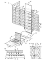
図1に本発明の貼りあわせ装置及び半導体装置の製造装置の一形態を示す。貼りあわせ装置は、第1の部品が配置された支持手段、第1の部品を保持する第1のフレキシブル基板、支持手段上に配置された第1の部品を第1のフレキシブル基板に仮着させるピックアップ手段を有する。また、第2の部品が配置された第2のフレキシブル基板、第2の部品に第1の部品を接続するボンディング手段を有する。また、第1のフレキシブル基板を供給する(繰り出す)第1の供給部、及び第1のフレキシブル基板を回収する(繰り込む)第1の回収部で構成される第1の基板搬送手段を有する。また、第2のフレキシブル基板を供給する(繰り出す)第2の供給部、第2のフレキシブル基板を回収する(繰り込む)第2の回収部で構成される第2の基板搬送手段を有する。第2の供給部の動作、第2の回収部の動作、及びローラーの回転速度により、第2のフレキシブル基板の移動タイミング及び移動速度を制御することができる。 FIG. 1 shows an embodiment of a bonding apparatus and a semiconductor device manufacturing apparatus according to the present invention. The laminating apparatus temporarily attaches the first component arranged on the support means on which the first component is arranged, the first flexible substrate holding the first component, and the first component arranged on the support means to the first flexible substrate. It has a pickup means. Also, a second flexible substrate on which the second component is arranged, and a bonding means for connecting the first component to the second component. In addition, the apparatus includes a first substrate transport unit configured by a first supply unit that supplies (feeds out) the first flexible substrate and a first recovery unit that recovers (feeds in) the first flexible substrate. In addition, there is provided a second substrate transport unit configured by a second supply unit that supplies (feeds out) the second flexible substrate and a second recovery unit that recovers (feeds in) the second flexible substrate. The movement timing and movement speed of the second flexible substrate can be controlled by the operation of the second supply unit, the operation of the second recovery unit, and the rotation speed of the roller.
以下に、第1の部品として半導体集積回路を用い、第2の部品としてアンテナを用いた半導体装置の製造装置の形態について示す。なお、第1の部品として、半導体集積回路の代わりに、アンテナ、第2の半導体集積回路、センサー、電池、配線基板、表示装置、MEMS(Micro Electro Mechanical System、マイクロマシン)等を適宜用いることができる。また、第2の部品として、アンテナの代わりに、半導体集積回路、センサー、電池、配線基板、表示装置、MEMS等を適宜用いることができる。 A semiconductor device manufacturing apparatus using a semiconductor integrated circuit as the first component and an antenna as the second component will be described below. As the first component, an antenna, a second semiconductor integrated circuit, a sensor, a battery, a wiring board, a display device, a MEMS (Micro Electro Mechanical System, micromachine), or the like can be used as appropriate instead of the semiconductor integrated circuit. . As the second component, a semiconductor integrated circuit, a sensor, a battery, a wiring board, a display device, a MEMS, or the like can be used as appropriate instead of the antenna.
半導体装置の製造装置は、半導体集積回路24が配置された支持手段20、半導体集積回路24を保持する第1のフレキシブル基板23、支持手段20上に配置された半導体集積回路24を第1のフレキシブル基板23に仮着させるピックアップ手段21を有する。また、アンテナ26が形成された第2のフレキシブル基板25、アンテナ26に半導体集積回路24を接続するボンディング手段22を有する。また、第1のフレキシブル基板23の移動を制御するローラー30、第2のフレキシブル基板25の移動を制御するローラー31を有してもよい。
The semiconductor device manufacturing apparatus includes a
図1(B)に、図1(A)のA−Bの断面図を示す。なお、図1のA−Bは半導体集積回路の列方向の断面図である。図1(B)に一形態を示すように、支持手段20上の半導体集積回路24上に、一定の間隔を置いて第1のフレキシブル基板23が配置される。さらには、第1のフレキシブル基板23上には、一定の間隔を置いてピックアップ手段21が配置される。ピックアップ手段21は押圧部34を有する。さらには、支持手段20及びピックアップ手段21の位置が第1のフレキシブル基板23及び半導体集積回路24を介して反対に設けてもよい。
FIG. 1B is a cross-sectional view taken along line AB of FIG. 1 is a cross-sectional view of the semiconductor integrated circuit in the column direction. As shown in FIG. 1B, the first
図1(C)に図1(A)のC−Dの断面図を示す。なお、図1(A)のC−Dはアンテナの列方向の断面図である。アンテナの各行間隔はaである。図1(C)に一形態を示すように、第1のフレキシブル基板23上の半導体集積回路24と一定の間隔を置いて、第2のフレキシブル基板25上のアンテナ26が対向する。また、第2のフレキシブル基板25と一定の間隔をおいて、ボンディング手段22が配置される。ボンディング手段22は押圧部33を有する。さらには、第1のフレキシブル基板23及び第2のフレキシブル基板25を介してボンディング手段22の反対側に、第1のフレキシブル基板23上の半導体集積回路24及び第2のフレキシブル基板25上のアンテナ26の接続を促すため、即ちボンディング手段22の加圧をしやすくするため、基板32を設けてもよい。さらには、基板32及びボンディング手段22の位置が第1のフレキシブル基板23及び第2のフレキシブル基板25を介して反対に設けてもよい。
FIG. 1C is a cross-sectional view taken along a line CD in FIG. Note that CD in FIG. 1A is a cross-sectional view in the column direction of the antenna. Each line spacing of the antenna is a. As shown in FIG. 1C, the
また、図示しないが、第1のフレキシブル基板23を供給する(繰り出す)第1の供給部、第1のフレキシブル基板を回収する(繰り込む)第1の回収部で構成される第1の基板搬送手段を有する。第1の供給部の動作、第1の回収部の動作、及びローラー30の回転速度により、第1のフレキシブル基板23の繰り出しタイミング及び移動速度を制御することができる。また、第2のフレキシブル基板25を供給する(繰り出す)第2の供給部、第2のフレキシブル基板25を回収する(繰り込む)第2の回収部で構成される第2の基板搬送手段を有する。第2の供給部の動作、第2の回収部の動作、及びローラー31の回転速度により、第2のフレキシブル基板25の移動タイミング及び移動速度を制御することができる。
Moreover, although not shown in figure, the 1st board | substrate conveyance comprised by the 1st collection | recovery part which collect | recovers (feeds in) the 1st supply part and 1st supply part which supplies (feeds out) the 1st
また、支持手段20、ピックアップ手段21、ボンディング手段22、第1の基板搬送手段、第2の基板搬送手段、ローラー30、31等の動作を制御する制御装置を有する。
In addition, the apparatus includes a control device that controls operations of the
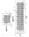
本半導体装置の製造装置においては、図2(A)に一形態を示すように、支持手段20上に半導体集積回路24がm行n列のマトリクス状に配置される。このときの半導体集積回路の行間隔をx、列間隔をyとする。なお、ここでは、半導体集積回路の行間隔及び列間隔は、隣接する半導体集積回路の中心間の距離とする。さらには、第1のフレキシブル基板23が移動する矢印37と平行な方向を、マトリクス状に配置された半導体集積回路の行方向とする。半導体集積回路の各々の内部には、アライメントマークが設けてあることが好ましい。
In the semiconductor device manufacturing apparatus, as shown in FIG. 2A, semiconductor integrated
本半導体装置の製造装置においては、図2(B)に一形態を示すように、第2のフレキシブル基板25上にアンテナ26がq行p列のマトリクス状に配置される。このときの隣接するアンテナの接続部29の行間隔をb、列間隔をaとする。なお、ここでは、アンテナの接続部の行間隔及び列間隔は、隣接するアンテナの接続部の中心間の距離とする。さらには、第2のフレキシブル基板25が移動する矢印35と平行な方向を、マトリクス状に配置されたアンテナの行方向とする。アンテナの各々の内部には、アライメントマークが設けてあることが好ましい。または、第2のフレキシブル基板には、アライメントマークが設けてあることが好ましい。アンテナと半導体集積回路を接続させるとき、それぞれのアライメントマークをそろえることで、歩留まり高く接続させることができる。
In the semiconductor device manufacturing apparatus, as shown in FIG. 2B,
なお、ここでは、アンテナ26の接続部29は、半導体集積回路24と同様の面積の形態について説明する。また、アンテナ26の接続部29及び半導体集積回路24の面積が異なっていても良い。即ち、半導体装置の作製装置の位置合わせ精度によって、アンテナ26の接続部29及び半導体集積回路24が完全に重畳せず若干ずれることもあるが、半導体集積回路24の接続端子及びアンテナ26が電気的に接続されていればよい。
Here, the
支持手段20は、半導体集積回路24を搭載するステージやトレイ、UVシートが張られたエキスパンドリング等がある。また、支持手段20は移動装置に設けられていてもよい。移動装置としては、水平移動(xy方向)が可能なベルトコンベヤー、昇降及び水平移動(xyz方向)が可能なロボットアームやステージ等がある。
The support means 20 includes a stage and tray on which the semiconductor integrated
ピックアップ手段21は、押圧部34を有する。また、ピックアップ手段21には、ロボットアーム、ヘッド、ローラー等の移動装置が接続されている。このような移動装置が設けられることにより、ピックアップ手段の昇降及び水平移動(xyz方向)を自由に行うことが可能である。ピックアップ手段21は、第1のフレキシブル基板23及び半導体集積回路24を圧着し、支持手段20から第1のフレキシブル基板23へ半導体集積回路24を移動させることができる。押圧部34は、半導体集積回路ごとに設けられてもよい。また、押圧する領域全体に一つの押圧部34を設けてもよい。ここでは、半導体集積回路ことに押圧部34が設けられている形態を示す。なお、押圧部34は10g〜100kg、好ましくは50g〜50kgの荷重が可能であることが好ましい。
The pickup means 21 has a
半導体集積回路24は、複数の半導体素子により回路が構成されるものであり、代表的には、複数の半導体素子が形成されるシリコンチップや、複数の薄膜半導体素子を有するチップ等がある。
The semiconductor integrated
複数の半導体素子が形成されるシリコンチップの作製方法の代表例としては、シリコンウエハの表面にMOSトランジスタや、容量、抵抗、ダイオード等を形成する。次に、シリコンウエハの裏面をバックグラインドと呼ばれる研磨処理行い、シリコンウエハの厚さを30〜250μm、好ましくは50〜100μmにする。この後、ダイサーで矩形状にシリコンウエハを分割したチップである。 As a typical example of a method for manufacturing a silicon chip on which a plurality of semiconductor elements are formed, a MOS transistor, a capacitor, a resistor, a diode, and the like are formed on the surface of a silicon wafer. Next, the back surface of the silicon wafer is subjected to a polishing process called back grinding so that the thickness of the silicon wafer is 30 to 250 μm, preferably 50 to 100 μm. Thereafter, the silicon wafer is divided into rectangular shapes by a dicer.
複数の薄膜半導体素子を有するチップの代表例としては、薄膜トランジスタ、容量、抵抗、薄膜ダイオード等を有する層である。薄膜半導体素子を有するチップの作製方法の代表例としては、基板上に、薄膜トランジスタ、容量、抵抗、薄膜ダイオード等を有する層を形成し、当該層を基板から剥離し、矩形状に分断することにより形成される。 A typical example of a chip having a plurality of thin film semiconductor elements is a layer having a thin film transistor, a capacitor, a resistor, a thin film diode, and the like. As a typical example of a method for manufacturing a chip having a thin film semiconductor element, a layer having a thin film transistor, a capacitor, a resistor, a thin film diode, and the like is formed over a substrate, and the layer is separated from the substrate and divided into rectangular shapes. It is formed.
第1のフレキシブル基板23は、表面において半導体集積回路24を保持するため、表面に粘着層を有する可撓性を有する基板(以下、粘着層を有するフィルムとも示す。)が好ましい。粘着層を有するフィルムとしては、紫外線硬化型粘着フィルム(UVフィルム、UVテープ、UVシートともいう。)や、圧力が加わることにより粘着力が変化する感圧フィルム(感圧フィルム、感圧テープ、感圧シートともいう。)、熱硬化型粘着フィルム(熱硬化型粘着テープ、熱硬化型粘着シートともいう。)等がある。さらには、粘着層を有するフィルムはエキスパンドタイプの伸縮可能なものであってもよい。
The first
一方、第2のフレキシブル基板25は、可撓性を有する可撓性基板を用いる。さらには、第2のフレキシブル基板25には、粘着層及び離型紙が設けられていても良い。このような場合は、アンテナが形成される面とは反対側に粘着層及び離型紙が設けられる。代表的な可撓性を有する基板には、PET(ポリエチレンテレフタレート)、PEN(ポリエチレンナフタレート)、PES(ポリエーテルスルホン)、ポリプロピレン、ポリプロピレンサルファイド、ポリカーボネート、ポリエーテルイミド、ポリフェニレンサルファイド、ポリフェニレンオキサイド、ポリサルフォン、ポリフタールアミド等からなる基板がある。また、繊維質な材料からなる紙がある。さらには、熱可塑性材料で形成される層として接着性有機樹脂(アクリル樹脂、エポキシ樹脂、シリコーン樹脂等)が上記可撓性を有する基板のアンテナが形成される面とは反対側に積層された基板を用いることができる。
On the other hand, the second
ボンディング手段22は、押圧部33により半導体集積回路24及びアンテナ26を圧着し、半導体集積回路24とアンテナ26とを実装(本圧着)させる手段である。なお、半導体集積回路24及びアンテナ26の間に導電性ペーストを設けることで、更に半導体集積回路24及びアンテナ26を確実に接続することができる。
The bonding means 22 is means for pressure-bonding the semiconductor integrated
ボンディング手段22は、押圧部33によりアンテナ及び半導体集積回路を加熱しながら圧着することにより、アンテナと半導体集積回路とを電気的に接続しても良い。このような場合、ボンディング手段22の押圧部に圧着手段及び加熱手段を設ける。このようなボンディング手段としては、熱圧着法や超音波接合法を用いたものあり、代表的には押圧部にヒーターや超音波ホーンを用いることができる。このような構成とすることで、別途大型のヒーターを設ける必要が無いため、半導体装置の製造装置の小型化が可能である。
The bonding means 22 may electrically connect the antenna and the semiconductor integrated circuit by pressing the antenna and the semiconductor integrated circuit while heating them with the
また、ボンディング手段22の押圧部33として圧着手段のみを用いる場合、別途アンテナ及び半導体集積回路の接続部を電気的に接続させるための加熱手段を設ける。このような加熱手段としては、ヒーターがある。このような構成とすることで、ボンディング手段による位置合わせの精度を高めるとともに、接着時間の短縮が可能である。この結果、複数のアンテナに対して第1のフレキシブル基板上に仮着された複数の半導体集積回路をボンディング手段により短時間で精度よく接続することができ、別途設けた加熱手段によりアンテナと半導体集積回路を電気的により確実に接続することができる。
When only the pressure bonding means is used as the
なお、アンテナ及び半導体集積回路を接続させるための加熱手段としては、室温から500℃までの加熱が可能なヒーターが好ましい。また、押圧部33は10g〜100kg、好ましくは50g〜50kgの荷重が可能であることが好ましい。
Note that a heater capable of heating from room temperature to 500 ° C. is preferable as a heating means for connecting the antenna and the semiconductor integrated circuit. Moreover, it is preferable that the
アンテナ26は、印刷法、導電性薄膜をエッチングする方法、メッキ方式等の手法により可撓性基板上に形成された導電層を用いることができる。アンテナ26は、Ag、Au、Cu、Ni、Pt、Pd、Ir、Rh、W、Al、Ta、Mo、Cd、Zn、Fe、Ti、Zr、及びBaのいずれか一つ以上の元素を有する導電層で形成することができる。
As the
図20に本発明に適応可能なアンテナの上面図を示す。アンテナとして機能する導電層の形状は、半導体装置における信号の伝送方式が電磁結合方式または電磁誘導方式(例えば13.56MHz帯)を適用する場合には、磁界密度の変化による電磁誘導を利用するため、図20(A)に示すように、方形コイル状281や、円形コイル状(例えば、スパイラルアンテナ)とすることができる。また、図20(B)に示すように方形ループ状282や円形ループ状とすることができる。
FIG. 20 shows a top view of an antenna applicable to the present invention. The shape of the conductive layer functioning as an antenna uses electromagnetic induction due to a change in magnetic field density when a signal transmission method in a semiconductor device employs an electromagnetic coupling method or an electromagnetic induction method (for example, 13.56 MHz band). As shown in FIG. 20A, a
また、マイクロ波方式(例えば、UHF帯(860〜960MHz帯)、2.45GHz帯等)を適用する場合には、信号の伝送に用いる電磁波の波長を考慮してアンテナとして機能する導電層の長さ等の形状を適宜設定すればよく、図20(C)に示すように直線型ダイポール状283や曲線型ダイポール状、面状(例えば、パッチアンテナ)とすることができる。
When a microwave method (for example, UHF band (860 to 960 MHz band), 2.45 GHz band, or the like) is applied, the length of the conductive layer that functions as an antenna in consideration of the wavelength of an electromagnetic wave used for signal transmission Such a shape may be set as appropriate, and as shown in FIG. 20C, a
なお、第2のフレキシブル基板25上にアンテナ26が形成されている形態をここでは示しているが、これに限定されるものではない。例えば、アンテナ26の代わりに、第2の半導体集積回路、センサー、電池、配線基板、表示装置等を適宜用いることができる。
In addition, although the form in which the
ローラー30、31、第1の供給部、第2の供給部、第1の回収部、第2の回収部は、円筒状の回転体であり、代表的には、表面の磨かれた円筒状の鋳造品やプラスチック等に相当する。ローラー30、31、第1の供給部、第2の供給部の各々は、所定の速度で回転する。また、第1の供給部、ローラー30、及び第1の回収部は、同じ方向に回転する。また、第2の供給部、ローラー31、及び第2の回収部は、同じ方向に回転する。
The
基板32は、ボンディング手段22を用いて半導体集積回路24及びアンテナ26を接続するときに、ボンディング手段22が押圧しやすいように設ける。このため、基板32は板状の部材、ローラー等適宜用いることができる。
The
図示しないが、制御手段としては、ピックアップ手段21及び半導体集積回路24の位置を検出する検出素子を有する。また、第1のフレキシブル基板23上の半導体集積回路24及びボンディング手段22の位置を検出する検出素子を有する。また、ピックアップ手段21、第1の供給部、ローラー30、第1の回収部、ボンディング装置、第2の供給部、ローラー31、第2の回収部等それぞれ駆動させる駆動部を有する。また、当該駆動部を駆動させる駆動回路を有する。
Although not shown, the control means includes a detection element for detecting the positions of the pickup means 21 and the semiconductor integrated
検出素子としては、CCDカメラ等を用いることが可能であり、検出素子で検出した画像情報を画像処理して、半導体集積回路、アンテナの接続端子やアライメントマークの位置を検出する。駆動部としては、モーターを用いることが可能であり、駆動回路から送られる信号により、駆動部が駆動される。駆動回路としては、マイクロコンピュータを用いることが可能である。具体的には、中央演算処理装置、記憶部であるROM及びRAMから構成され、検出素子で検出した画像情報や駆動部の駆動情報等を一時的にRAMに保存するとともに、ROMに記録されているプログラム及びRAMに保存された情報により駆動部を駆動させる信号を駆動部に送り出す。 A CCD camera or the like can be used as the detection element, and image information detected by the detection element is subjected to image processing to detect the positions of the semiconductor integrated circuit, the connection terminal of the antenna, and the alignment mark. A motor can be used as the drive unit, and the drive unit is driven by a signal sent from the drive circuit. A microcomputer can be used as the drive circuit. Specifically, it is composed of a central processing unit, ROM and RAM that are storage units, and temporarily stores image information detected by the detection element, drive information of the drive unit, etc. in the RAM, and is recorded in the ROM. A signal for driving the drive unit is sent to the drive unit based on the stored program and information stored in the RAM.
さらに制御手段は、サーバー、他のパーソナルコンピュータ等に接続されていてもよい。 Furthermore, the control means may be connected to a server, another personal computer, or the like.
制御手段により、ピックアップ手段21を用いて半導体集積回路24を第1のフレキシブル基板23に仮着させるタイミング及びピックアップ手段21の圧力を制御する。また、第1の供給部、ローラー30、第1の回収部の回転速度その及び回転動作を制御する。また、ボンディング手段22を第2のフレキシブル基板25及び半導体集積回路24に押圧するタイミング及びボンディング手段22の圧力を制御する。また、第2の供給部、ローラー31、第2の回収部の回転速度その及び回転動作を制御する。
The control means controls the timing at which the semiconductor integrated
なお、支持手段20及びピックアップ手段21の間に、フリップチップ手段を有してもよい。フリップチップ手段としては、回転機能を有するピックアップ手段が好ましい。代表的には、持着部を有するローラーやヘッドがある。持着部の代表例としては、ピンセットや爪等の把持具、コレット、又は吸着することが可能なノズル等がある。
A flip chip unit may be provided between the
次に、上記貼りあわせ装置を用いた、第1の部品及び第2の部品の貼りあわせ方法について、以下に示す。 Next, a method for bonding the first component and the second component using the bonding apparatus will be described below.
ここでは、第1のフレキシブル基板及び第2のフレキシブル基板の各々の面が対向し、かつ各基板の長辺、即ち移動方向が90度に交差し、第1の部品の行及び列が90度に交差し、第2の部品の行及び列が90度に交差する形態について示す。 Here, the surfaces of the first flexible substrate and the second flexible substrate are opposed to each other, and the long sides of each substrate, that is, the moving direction intersects at 90 degrees, and the rows and columns of the first components are 90 degrees. And the second part row and column intersect at 90 degrees.
m行n列のマトリクス状に配置された第1の部品と、q行p列のマトリクス状に配置された第2の部品とを有する。第1のフレキシブル基板を移動させながら、ピックアップ手段をp回押圧して、第1のフレキシブル基板に第1の部品をp行分仮着する。このときの第1のフレキシブル基板の移動距離はpaである。次に、第1のフレキシブル基板の移動を停止する。次に、ボンディング手段を押圧し、第1のフレキシブル基板上の第1の部品を、第2のフレキシブル基板上の第2の部品に接続した後、第2のフレキシブル基板を距離b移動する。ボンディング手段の押圧及び第2のフレキシブル基板の移動をn回繰り返す。この結果、p行分の第1の部品を第2の部品に貼り付けることができる。この後、再度第1のフレキシブル基板を移動させながら、ピックアップ手段をp回押圧して、上記の動作を繰り返すことにより、m行n列のマトリクス状に配置された第1の部品と、q行p列のマトリクス状に配置された第2の部品を貼りあわせることができる。 The first component is arranged in a matrix of m rows and n columns, and the second component is arranged in a matrix of q rows and p columns. While moving the first flexible substrate, the pickup means is pressed p times to temporarily attach the first component to the first flexible substrate for p rows. At this time, the moving distance of the first flexible substrate is pa. Next, the movement of the first flexible substrate is stopped. Next, after pressing the bonding means to connect the first component on the first flexible substrate to the second component on the second flexible substrate, the second flexible substrate is moved by the distance b. The pressing of the bonding means and the movement of the second flexible substrate are repeated n times. As a result, the first part for p rows can be attached to the second part. After that, by moving the first flexible substrate again and pressing the pickup means p times and repeating the above operation, the first component arranged in a matrix of m rows and n columns and q rows The second parts arranged in a matrix of p columns can be bonded together.
以下、第1の部品として半導体集積回路を用い、第2の部品としてアンテナを用いて、半導体装置を作製する方法について、図1、図3、図5及び図6を用いて説明する。なお、以下の説明において、i行j列を(i、j)とも示す。 Hereinafter, a method for manufacturing a semiconductor device using a semiconductor integrated circuit as the first component and an antenna as the second component will be described with reference to FIGS. 1, 3, 5, and 6. In the following description, i row and j column are also indicated as (i, j).
第1のフレキシブル基板23に半導体集積回路24を仮着させる方法について、図1及び図3を用いて説明する。図3は図1のA−Bの断面図である。図3(A)は図1(B)と同様の図であり、支持手段20上に配置された半導体集積回路24と、半導体集積回路24の上に一定の距離を置いて配置される第1のフレキシブル基板23と、第1のフレキシブル基板23上に一定の距離を置いて配置されるピックアップ手段21が配置される。
A method for temporarily attaching the semiconductor integrated
図3(B)に示すように、駆動部によりピックアップ手段21を支持手段20に押圧する。または、支持手段20をピックアップ手段に押圧する。この結果、ピックアップ手段21により第1のフレキシブル基板23に半導体集積回路24を仮着させることができる。このとき、制御装置により、第1のフレキシブル基板23に半導体集積回路24を仮着させるタイミングを制御することにより、図1に示すように、半導体集積回路の行間隔をxからaとする。なお、間隔aは、第2のフレキシブル基板25に設けられる隣接するアンテナの各列の接続部の間隔である。次に、図3(C)に示すように、駆動部によりピックアップ手段21また支持手段20を元の位置に戻す。以上の工程により、第1のフレキシブル基板23に半導体集積回路24を仮着させることができる。
As shown in FIG. 3B, the
ここで、支持手段20上に配置された半導体集積回路24において、接続端子が形成される面によって、第1のフレキシブル基板23に半導体集積回路24を仮着させる方法が異なる形態について、図5及び6を用いて示す。
Here, in the semiconductor integrated
図5(A)乃至(C)は、図1のA−Bの一部において、半導体集積回路24を第1のフレキシブル基板23に仮着させる工程について示す。
5A to 5C show a process of temporarily attaching the semiconductor integrated
図5では、半導体集積回路24の接続端子24aは支持手段20に対向しており、接続端子24aの接続面がピックアップ手段21側に露出していない形態について説明する。なお、このように、半導体集積回路24の接続端子24aが支持手段20に対向する構成としては、半導体集積回路24内部に、半導体素子と接続するスルーホールを形成し、該スルーホールを充填するプラグを接続端子24aとしてもよい。また、半導体集積回路24の表面に接続端子24aを形成した後、接続端子24aが支持手段20に対向するように、半導体集積回路を反転させて支持手段20に設けてもよい。
In FIG. 5, the
この場合は、図1で示す半導体装置の製造装置によって、半導体集積回路24及びアンテナ26を接続させることができる。具体的には、図5(B)に示すように、駆動部によりピックアップ手段21を支持手段20に押圧する。または、支持手段20をピックアップ手段に押圧する。次に、図5(C)に示すように、駆動部によりピックアップ手段21また支持手段20を元の位置に戻す。以上の工程により、接続端子が露出するように第1のフレキシブル基板23に半導体集積回路24を仮着させることができる。
In this case, the semiconductor integrated
次に、半導体集積回路24の接続端子24aは支持手段20に対向しておらず、接続端子の接続面がピックアップ手段21側に露出している形態について図6を用いて説明する。図6(A)乃至(D)は、図1のA−Bの一部において、半導体集積回路24を第1のフレキシブル基板23に仮着させる工程について示す。
Next, a configuration in which the
この場合は、図5に示すような方法で半導体集積回路24を第1のフレキシブル基板23に仮着させても、接続端子24aの接続面が第1のフレキシブル基板23に対向してしまい、後にアンテナと接続端子24aを接続させることができない。このため、半導体装置の製造装置は、支持手段20からピックアップ手段21へ移動する間に、半導体集積回路24をひっくり返すフリップチップ手段を設ける。
In this case, even if the semiconductor integrated
フリップチップ手段としては、ローラーの表面に半導体集積回路を持着することが可能な持着部を有すればよい。また、180度以上回転可能なピックアップ手段であってもよい。 As the flip chip means, it is only necessary to have a holding part capable of holding the semiconductor integrated circuit on the surface of the roller. Further, it may be pick-up means capable of rotating 180 degrees or more.
具体的には、図6(B)に示すように、駆動部によりフリップチップ手段36を支持手段20に押圧する。または、支持手段20をフリップチップ手段に押圧する。この後、駆動部によりフリップチップ手段36または支持手段20を元の位置に戻して、フリップチップ手段36は半導体集積回路24を持着する。このとき、フリップチップ手段36は、半導体集積回路24の接続端子24aが形成される面において半導体集積回路24を持着している。
Specifically, as shown in FIG. 6B, the flip chip means 36 is pressed against the support means 20 by the drive unit. Alternatively, the support means 20 is pressed against the flip chip means. Thereafter, the
次に、駆動部によりフリップチップ手段36を180度回転させて、図6(C)に示すように、半導体集積回路24の接続端子24aが形成される面の反対側と第1のフレキシブル基板23とが対向するように配置する。さらには、検出素子及び駆動部により、半導体集積回路24の接続端子24aが形成される面の反対側と、ピックアップ手段21の押圧部34とが第1のフレキシブル基板23を介して対向するように配置する。
Next, the flip chip means 36 is rotated 180 degrees by the drive unit, and as shown in FIG. 6C, the opposite side of the surface on which the
次に、図6(D)に示すように、駆動部によりピックアップ手段21をフリップチップ手段36に押圧する。または、フリップチップ手段36をピックアップ手段21に押圧する。この後、ピックアップ手段21またはフリップチップ手段36を元の位置に戻して、図6(E)に示すように、接続端子24aが露出するように半導体集積回路24を第1のフレキシブル基板23に仮着させる。
Next, as shown in FIG. 6D, the pickup means 21 is pressed against the flip chip means 36 by the drive unit. Alternatively, the flip chip means 36 is pressed against the pickup means 21. Thereafter, the pickup means 21 or the flip chip means 36 is returned to the original position, and the semiconductor integrated
以上の工程により、第1のフレキシブル基板23に半導体集積回路24を仮着させることができる。
Through the above steps, the semiconductor integrated
次に、第2のフレキシブル基板23上のアンテナ26及び半導体集積回路24を接続する方法について、図1、図4、図7乃至図11を用いて説明する。なお、図7乃至図11において、半導体集積回路は実線で表しているが、実際には半導体集積回路及びアンテナが対向しており、対向している半導体集積回路及びアンテナの外側にそれぞれ第1のフレキシブル基板23及び第2のフレキシブル基板25が設けられている。即ち、図7乃至11においては、第1のフレキシブル基板23が手前で、半導体集積回路、アンテナ、及び第2のフレキシブル基板が順に奥に配置されていることになる。
Next, a method for connecting the
はじめに、半導体集積回路24及びボンディング手段の位置を検出する検出素子を用いて、アンテナの接続部29及び半導体集積回路24の接続端子を位置合わせする。具体的には、図4(A)に示すように、第1のフレキシブル基板23上の半導体集積回路24が、第2のフレキシブル基板25上のアンテナ26の接続部と対向するように、第1のフレキシブル基板23及び第2のフレキシブル基板25の位置を、検出素子及び駆動部により制御する。
First, the
次に、図4(B)に示すように、駆動部によりボンディング手段22を基板32に押圧する。具体的には、図7(A)に示すように、1行1列からp行1列の半導体集積回路40と、1行1列から1行p列のアンテナ41をそれぞれ接続させる。次に、図3(C)に示すように、駆動部によりボンディング手段22を元の位置に戻す。以上の工程により、第2のフレキシブル基板25上のアンテナ26と半導体集積回路24を接続することができる。
Next, as shown in FIG. 4B, the
次に、図7(B)に示すように、第1のフレキシブル基板23を固定したまま、駆動部により第2の基板搬送手段を動かして第2のフレキシブル基板25を矢印35の方向にb−y移動する。
Next, as shown in FIG. 7B, the second
ここで、第2のフレキシブル基板25の移動距離に関して図8を用いて説明する。図8では、図7(A)において1行1列〜1行n列の半導体集積回路及び1行1列のアンテナ及び2行1列のアンテナについて拡大したものを示す。
Here, the moving distance of the second
半導体集積回路45((1,1))が接続されたアンテナ46((1,1))の接続部と、隣の行のアンテナ48((2,1))の接続部29の間隔はbである。一方、アンテナ46と接続された半導体集積回路45((1,1))と、隣の列の半導体集積回路47((1,2))の間隔はyである。
The distance between the connection portion of the antenna 46 ((1, 1)) to which the semiconductor integrated circuit 45 ((1, 1)) is connected and the
半導体集積回路45((1,1))及びアンテナ46((1,1))を接続した後、半導体集積回路47((1,2))及びアンテナ48((2,1))を接続させるためには、第2の基板搬送手段により第2のフレキシブル基板25を矢印35の方向に移動させ、アンテナ48の接続部29と半導体集積回路47とを対向させればよい。即ち、第1のフレキシブル基板23上の半導体集積回路47の位置と、アンテナ48の接続部29が一致するように、第2のフレキシブル基板25を矢印35方向へ移動すればよい。このため、第2のフレキシブル基板25の移動距離はb−yである。
After the semiconductor integrated circuit 45 ((1, 1)) and the antenna 46 ((1, 1)) are connected, the semiconductor integrated circuit 47 ((1, 2)) and the antenna 48 ((2, 1)) are connected. For this purpose, the second
図7(B)に示すように、第2のフレキシブル基板25を矢印35方向へ移動させた後、ボンディング手段22によって、アンテナ及び半導体集積回路を押圧することにより、1行2列からp行2列の半導体集積回路43と、2行1列から2行p列のアンテナ44をそれぞれ接続させることができる。
As shown in FIG. 7B, after the second
この後、半導体集積回路及びアンテナの接続、並びに第2のフレキシブル基板の移動を繰り返すことにより、(3,1)〜(3,p)から(n−1,1)〜(n−1,p)の半導体集積回路をアンテナに接続することができる。 Thereafter, the connection of the semiconductor integrated circuit and the antenna and the movement of the second flexible substrate are repeated, so that (3, 1) to (3, p) to (n-1, 1) to (n-1, p). ) Can be connected to the antenna.
次に、図9(A)に示すように、1行n列からp行n列の半導体集積回路60と、n行1列からn行p列のアンテナ61をそれぞれ接続する。この結果、第1のフレキシブル基板上の1行からp行の半導体集積回路は、すべて第2のフレキシブル基板25上のアンテナに仮着される。よって、第1のフレキシブル基板23を矢印37の方向にpa移動し、第2のフレキシブル基板25を矢印35の方向にb+(n−1)y移動する。この結果、図9(B)に示すように、(1+p,1)〜(p+p,1)の半導体集積回路及び(n+1,1)〜(n+1,p)行のアンテナを対向させることができる。このため、(1+p,1)〜(p+p,1)の半導体集積回路63と、(n+1,1)〜(n+1,p)のアンテナ64の接続部が対向する。これらをボンディング手段により押圧することで、それぞれを接続することができる。
Next, as shown in FIG. 9A, a semiconductor integrated
ここで、第1のフレキシブル基板23及び第2のフレキシブル基板25の移動距離に関して、図10を用いて説明する。なお、ここでは、1行n列の半導体集積回路65及びn行1列のアンテナ66の接続部を接続した後、(1+p)行1列の半導体集積回路67及び(n+1)行1列のアンテナ68の接続部を接続させる例を用いて説明する。
Here, the movement distance of the first
はじめに、アンテナの行方向における移動距離について、図10を用いて示す。図9(A)で半導体集積回路が接続されたアンテナ61の一部であるn行1列のアンテナ66の接続部と、隣の行((n+1)行1列)のアンテナ68の接続部69の間隔はbである。一方、半導体集積回路の列方向における間隔はyである。また、半導体集積回路は1〜n列設けられている。このため、第1のフレキシブル基板23上の半導体集積回路67の位置と、アンテナ68の接続部69を一致させるためには、第2のフレキシブル基板25を矢印35方向においては、b+(n−1)y移動すればよい。
First, the moving distance of the antenna in the row direction will be described with reference to FIG. In FIG. 9A, a connection portion of the
次に、半導体集積回路の行方向における移動距離について、同様に図10を用いて示す。半導体集積回路の行方向における間隔はaである。また、アンテナは1〜p列設けられている。このため、第1のフレキシブル基板23上の半導体集積回路67の位置と、アンテナ68の接続部69が一致するためには、第2のフレキシブル基板25を矢印37方向へ、pa移動すればよい。
Next, the movement distance in the row direction of the semiconductor integrated circuit is similarly shown using FIG. The interval in the row direction of the semiconductor integrated circuit is a. The antenna is provided in 1 to p rows. For this reason, in order for the position of the semiconductor integrated
なお、ここで、1行からp行の半導体集積回路を第2のフレキシブル基板25上のアンテナと接続した後に、第1のフレキシブル基板23を矢印37に移動させる回数をuとすると、次にアンテナと貼りあわせる半導体集積回路は(1+up)行から(p+up)行である。また、当該半導体集積回路と貼りあわせられるアンテナは、(1+un)行から(n+un)行である(uは自然数)。
Here, if the number of times the first
また、図11に示すように、i行j列の半導体集積回路80を、j行i列のアンテナ81と接続する。次に、矢印35方向に第2のフレキシブル基板25を移動した後、i行(j+1)列の半導体集積回路82を、(j+1)行i列のアンテナ83と接続することができる。
Further, as shown in FIG. 11, the semiconductor integrated
さらには、半導体集積回路及びアンテナを封止するように、第2のフレキシブル基板表面に第3のフレキシブル基板を貼りあわせてもよい。この結果、半導体集積回路及びアンテナを密閉することができる。 Further, a third flexible substrate may be bonded to the surface of the second flexible substrate so as to seal the semiconductor integrated circuit and the antenna. As a result, the semiconductor integrated circuit and the antenna can be sealed.
この後、第2のフレキシブル基板、さらには第3のフレキシブル基板を適当な場所(例えば、図11の実線27)で切断することにより、半導体集積回路、アンテナ、及び切断された第2のフレキシブル基板、更には切断された第3のフレキシブル基板を有する半導体装置を作製することができる。
Thereafter, the semiconductor integrated circuit, the antenna, and the cut second flexible substrate are cut by cutting the second flexible substrate and further the third flexible substrate at an appropriate place (for example, the
本発明の半導体装置の製造装置、及び半導体装置の製造装置を用いた作製方法により、複数のアンテナの1行と、第1のフレキシブル基板上に仮着された複数の半導体集積回路のうち当該1行に対応する複数の半導体集積回路とを、同時にまたは連続して接続することができる。このため、一度のボンディング処理により複数の半導体装置を作製することが可能である。このため、半導体装置の量産性を高めることができる。 According to the semiconductor device manufacturing apparatus of the present invention and the manufacturing method using the semiconductor device manufacturing apparatus, one of the plurality of semiconductor integrated circuits temporarily attached to one row of the plurality of antennas and the first flexible substrate. A plurality of semiconductor integrated circuits corresponding to a row can be connected simultaneously or successively. Therefore, a plurality of semiconductor devices can be manufactured by a single bonding process. For this reason, the mass productivity of the semiconductor device can be improved.
(実施の形態2)
本実施の形態では、第1の部品及び第2の部品の行及び列がそれぞれ一定角度θで交差するように配置されている形態について説明する。
(Embodiment 2)
In the present embodiment, a mode in which the rows and columns of the first component and the second component are arranged so as to intersect each other at a constant angle θ will be described.
本実施の形態で示す貼りあわせ装置は、図1に示すように、第1のフレキシブル基板及び第2のフレキシブル基板の各々の面が対向し、かつ各基板の長辺、即ち移動方向が90度に交差しており、m行n列のマトリクス状に配置された第1の部品において、行と列がarctan(y/x)で交差している。また、q行p列のマトリクス状に配置された第2の部品において、行と列がarctan(y/a)で交差している。なお、上記構成に限らず、実施の形態1と同様に、m行n列のマトリクス状に配置された第1の部品において、行と列が90度で交差し、q行p列のマトリクス状に配置された第2の部品において、行と列が90度で交差し、第1のフレキシブル基板及び第2のフレキシブル基板の各々の面が対向し、かつ各基板の長辺、即ち移動方向がarctan(y/a)で交差していてもよい。 In the bonding apparatus shown in this embodiment, as shown in FIG. 1, the surfaces of the first flexible substrate and the second flexible substrate face each other, and the long sides of each substrate, that is, the moving direction is 90 degrees. In the first part arranged in a matrix of m rows and n columns, the rows and the columns intersect at arctan (y / x). In the second component arranged in a matrix of q rows and p columns, the rows and the columns intersect at arctan (y / a). Not limited to the above configuration, as in the first embodiment, in the first part arranged in a matrix of m rows and n columns, the rows and the columns intersect at 90 degrees, and a matrix of q rows and p columns is formed. In the second component arranged in the row, the rows and the columns intersect at 90 degrees, the surfaces of the first flexible substrate and the second flexible substrate face each other, and the long side of each substrate, that is, the moving direction is You may cross at arctan (y / a).
以下に、第1の部品として半導体集積回路を用い、第2の部品としてアンテナを用いた半導体装置の製造装置の形態について示す。なお、第1の部品として、半導体集積回路の代わりに、アンテナ、第2の半導体集積回路、センサー、電池、配線基板、表示装置、MEMS等を適宜用いることができる。また、第2の部品として、アンテナの代わりに、半導体集積回路、センサー、電池、配線基板、表示装置、MEMS等を適宜用いることができる。 A semiconductor device manufacturing apparatus using a semiconductor integrated circuit as the first component and an antenna as the second component will be described below. Note that as the first component, an antenna, a second semiconductor integrated circuit, a sensor, a battery, a wiring board, a display device, a MEMS, or the like can be used as appropriate instead of the semiconductor integrated circuit. As the second component, a semiconductor integrated circuit, a sensor, a battery, a wiring board, a display device, a MEMS, or the like can be used as appropriate instead of the antenna.
本半導体装置の製造装置においては、図12(A)に一形態を示すように、支持手段20上に半導体集積回路がm行n列のマトリクス状に配置される。このときの半導体集積回路の行間隔をx、列間隔をyとする。さらには、第1のフレキシブル基板23が移動する矢印37と平行な方向を、マトリクス状に配置された半導体集積回路の行方向とする。本実施の形態の半導体集積回路の行は半導体集積回路の列に対して角度θ1で交差している。
In this semiconductor device manufacturing apparatus, as shown in FIG. 12A, semiconductor integrated circuits are arranged in a matrix of m rows and n columns on the support means 20. In this case, the row interval of the semiconductor integrated circuit is x and the column interval is y. Furthermore, the direction parallel to the
本半導体装置の製造装置においては、図12(B)に一形態を示すように、第2のフレキシブル基板25上にアンテナ26がq行p列のマトリクス状に配置される。このときの隣接するアンテナの接続部75の行間隔をb、列間隔をaとする。また、第2のフレキシブル基板25が移動する矢印35と平行な方向を、マトリクス状に配置されたアンテナの行方向とする。さらには、アンテナの行はアンテナの列に対して角度θで交差している。
In this semiconductor device manufacturing apparatus, as shown in FIG. 12B,
なお、ここでは、アンテナ26の接続部75は、実施の形態1のアンテナ26の接続部29と同様に、半導体集積回路24と同様の面積である形態について説明する。また、アンテナ26の接続部29及び半導体集積回路24の面積が異なっていても良い。即ち、半導体装置の作製装置の位置合わせ精度によって、アンテナ26の接続部29及び半導体集積回路24が完全に重畳せず若干ずれることもあるが、半導体集積回路24の接続端子及びアンテナ26が電気的に接続されていればよい。
Here, a configuration in which the
次に、上記貼りあわせ装置を用いて、第1の部品及び第2の部品の貼りあわせ方法について、以下に示す。 Next, a method for bonding the first component and the second component using the bonding apparatus will be described below.
ここでは、第1のフレキシブル基板及び第2のフレキシブル基板の各々の面が対向し、かつ各基板の長辺、即ち移動方向が90度に交差し、第1の部品の行及び列がθ1=arctan(y/x)で交差し、第2の部品の行及び列がθ=arctan(y/a)度で交差する形態について示す。 Here, the surfaces of the first flexible substrate and the second flexible substrate face each other, and the long sides of each substrate, that is, the moving direction intersects at 90 degrees, and the row and column of the first component are θ1 = A mode of crossing at arctan (y / x) and a row and a column of the second part crossing at θ = arctan (y / a) degrees will be described.
m行n列のマトリクス状に配置された第1の部品と、q行p列のマトリクス状に配置された第2の部品とを有する。第1のフレキシブル基板を移動しながら、ピックアップ手段をp回以上押圧して、第1のフレキシブル基板に第1の部品をp行以上仮着する。このとき、第1のフレキシブル基板を移動させる距離はpa以上である。次に、第2のフレキシブル基板上の第2の部品に対応する領域に、第1のフレキシブル基板の第1の部品を移動させたらば、ボンディング手段を押圧し、第1のフレキシブル基板上の第1の部品を、第2のフレキシブル基板上の第2の部品に接続する。次に、第2のフレキシブル基板を距離b移動するとともに、第1のフレキシブル基板を距離a移動する。この後、ボンディング手段の押圧、第1のフレキシブル基板の移動、及び第2のフレキシブル基板の移動を繰り返す。このとき、第1のフレキシブル基板の速度をa、第2のフレキシブル基板の速度をbとすれば、第1の部品を第2の部品に連続的に貼り付けることができる。なお、ボンディング手段を押圧して第1の部品及び第2の部品を貼りあわせるときに、ピックアップ手段を押圧して支持手段上の第1の部品を第1のフレキシブル基板に仮着させればよい。 The first component is arranged in a matrix of m rows and n columns, and the second component is arranged in a matrix of q rows and p columns. While moving the first flexible substrate, the pickup means is pressed p times or more to temporarily attach the first component to the first flexible substrate by p rows or more. At this time, the distance to which the first flexible substrate is moved is pa or more. Next, when the first component of the first flexible substrate is moved to the area corresponding to the second component on the second flexible substrate, the bonding means is pressed, and the first component on the first flexible substrate is pressed. One component is connected to a second component on the second flexible substrate. Next, the second flexible substrate is moved by the distance b, and the first flexible substrate is moved by the distance a. Thereafter, the pressing of the bonding means, the movement of the first flexible substrate, and the movement of the second flexible substrate are repeated. At this time, if the speed of the first flexible substrate is a and the speed of the second flexible substrate is b, the first component can be continuously attached to the second component. When the bonding means is pressed to bond the first component and the second component, the pickup means may be pressed to temporarily attach the first component on the support means to the first flexible substrate. .
以下、第1の部品として半導体集積回路を用い、第2の部品としてアンテナを用いて、半導体装置を作製する方法について、図13及び14を用いて説明する。なお、図13及び14において、半導体集積回路は実線で表しているが、実際には半導体集積回路及びアンテナが対向しており、半導体集積回路及びアンテナが対向する面の外側にそれぞれ第1のフレキシブル基板23及び第2のフレキシブル基板25が設けられている。即ち、図13及び14においては、第1のフレキシブル基板23が手前で、半導体集積回路、アンテナ、及び第2のフレキシブル基板が順に奥に配置されていることになる。
Hereinafter, a method for manufacturing a semiconductor device using a semiconductor integrated circuit as the first component and an antenna as the second component will be described with reference to FIGS. 13 and 14, the semiconductor integrated circuit is indicated by a solid line. However, in actuality, the semiconductor integrated circuit and the antenna are opposed to each other, and the first flexible circuit is disposed outside the surface where the semiconductor integrated circuit and the antenna are opposed to each other. A
はじめに、実施の形態1と同様に第1のフレキシブル基板上に半導体集積回路を仮着させる。このとき、半導体集積回路の列の間隔がxからaとなるように仮着させる。 First, as in the first embodiment, a semiconductor integrated circuit is temporarily attached onto a first flexible substrate. At this time, the semiconductor integrated circuits are temporarily attached so that the interval between the columns is from x to a.
図13(A)に示すように、第1のフレキシブル基板23と第2のフレキシブル基板25が重なる領域において、破線76a上にあるi行の半導体集積回路は、当該半導体集積回路と対向するj行のアンテナ81の接続部において、接続される。なお、i行の半導体集積回路において、全ての半導体集積回路が同時にアンテナと接続されても良い。また、i行j列の半導体集積回路が接続されるタイミングとは別に、i行(j−1)列の半導体集積回路77及びi行(j+1)列のアンテナの接続部が接続されてもよい。
As shown in FIG. 13A, in the region where the first
この後、第1のフレキシブル基板23を矢印37の方向へ移動し、第2のフレキシブル基板25を矢印35の方向へ移動する。この結果、図13(B)にしめすように破線76b上の(i+1)行の半導体集積回路及び(j+1)行のアンテナ83の接続部を対向させることができる。
Thereafter, the first
このときの第1のフレキシブル基板23及び第2のフレキシブル基板25の移動距離、並びにアンテナの行及び列が交差する角度θを、図14(A)を用いて説明する。ここでは、i行j列の半導体集積回路70及びj行i列のアンテナ71を接続した後、(i+1)行j列の半導体集積回路72及び(j+1)行i列のアンテナを接続する例を用いて説明する。
The moving distance of the first
i行j列の半導体集積回路70及びj行i列のアンテナ71を接続した後、第1のフレキシブル基板23及び第2のフレキシブル基板25をそれぞれ移動して(i+1)行j列の半導体集積回路72及び(j+1)行i列のアンテナ73が対向するようにする。
After connecting the i row and j column semiconductor integrated
このためには、半導体集積回路70がアンテナ71と接続された領域に半導体集積回路72を移動させる。半導体集積回路70、72の間隔はaであるため、第1のフレキシブル基板23を矢印37の方向にa移動する。
For this purpose, the semiconductor integrated
一方、アンテナ71の接続部と半導体集積回路70を接続させた領域に、アンテナ73の接続部75を移動させる。アンテナ71及び73の接続部の間隔はbであるため、第2のフレキシブル基板25を矢印35の方向にb移動する。
On the other hand, the connecting
この結果、(i+1)行j列の半導体集積回路72及び(j+1)行i列のアンテナ73を対向させることができる。
As a result, the semiconductor integrated
なお、ここで、第1のフレキシブル基板23の移動速度がaであり、第2のフレキシブル基板の移動速度がbのとき、アンテナ及び半導体集積回路の接続を連続的に行うことができる。
Here, when the moving speed of the first
次に、第1のフレキシブル基板23に仮着された半導体集積回路の行及び列、即ちアンテナの行及び列方向がなす角度θについて、図14(B)を用いて説明する。第1のフレキシブル基板23に仮着された半導体集積回路の行は破線76a上に配置され、列は破線76c上に配置される。また、半導体集積回路の行及び列は角度θをなす。
Next, the angle θ formed by the row and column of the semiconductor integrated circuit temporarily attached to the first
同一列において隣接する半導体集積回路70、72の図12(A)に示す行方向の間隔はaである。また、同一行において隣接する半導体集積回路72、77の図12(A)に示す行方向の間隔はyである。これらの2つの距離から角度θは、arctan(y/a)である。
An interval in the row direction shown in FIG. 12A of adjacent semiconductor integrated
この後、図13(B)に示すように、対向した(i+1)行の半導体集積回路および(j+1)行のアンテナをボンディング手段により圧着して、半導体集積回路及びアンテナを接続する。 After that, as shown in FIG. 13B, the semiconductor integrated circuit and the antenna are connected to each other by bonding the (i + 1) -row semiconductor integrated circuits and the (j + 1) -row antennas by bonding means.
さらには、半導体集積回路及びアンテナを封止するように、第2のフレキシブル基板表面に第3のフレキシブル基板を貼りあわせてもよい。この結果、半導体集積回路及びアンテナを密閉することができる。 Further, a third flexible substrate may be bonded to the surface of the second flexible substrate so as to seal the semiconductor integrated circuit and the antenna. As a result, the semiconductor integrated circuit and the antenna can be sealed.
この後、第2のフレキシブル基板、さらには第3のフレキシブル基板を適当な場所(例えば、実線27)で切断することにより、半導体集積回路、アンテナ、及び切断された第2のフレキシブル基板、更には切断された第3のフレキシブル基板を有する半導体装置を作製することができる。 Thereafter, the second flexible substrate, and further the third flexible substrate is cut at an appropriate location (for example, the solid line 27), whereby the semiconductor integrated circuit, the antenna, and the cut second flexible substrate, A semiconductor device having the cut third flexible substrate can be manufactured.
本発明の半導体装置の製造装置、及び半導体装置の製造装置を用いた作製方法により、複数のアンテナの1行と、第1のフレキシブル基板上に仮着された複数の半導体集積回路のうち当該1行に対応する複数の半導体集積回路とを、同時にまたは連続して接続することができる。このため、一度のボンディング処理により複数の半導体装置を作製することが可能である。また、第1のフレキシブル基板及び第2のフレキシブル基板の繰り出しを同期させながら行うことが可能である。このため、半導体装置の量産性を高めることができる。 According to the semiconductor device manufacturing apparatus of the present invention and the manufacturing method using the semiconductor device manufacturing apparatus, one of the plurality of semiconductor integrated circuits temporarily attached to one row of the plurality of antennas and the first flexible substrate. A plurality of semiconductor integrated circuits corresponding to a row can be connected simultaneously or successively. Therefore, a plurality of semiconductor devices can be manufactured by a single bonding process. Further, it is possible to perform the feeding of the first flexible substrate and the second flexible substrate while synchronizing them. For this reason, the mass productivity of the semiconductor device can be improved.
本実施例では、非接触でデータの伝送が可能な半導体装置の作製工程を、図15〜17を用いて説明する。 In this embodiment, a manufacturing process of a semiconductor device capable of transmitting data without contact will be described with reference to FIGS.
図15(A)に示すように、基板1201上に剥離層1202を形成し、剥離層1202上に絶縁層1203を形成し、絶縁層1203上に薄膜トランジスタ1204及び薄膜トランジスタを構成する導電層を絶縁する層間絶縁層1205を形成し、薄膜トランジスタの半導体層に接続するソース電極及びドレイン電極1206を形成する。次に、薄膜トランジスタ1204、層間絶縁層1205、ソース電極及びドレイン電極1206を覆う絶縁層1207を形成し、絶縁層1207を介してソース電極またはドレイン電極1206に接続する導電層1208を形成する。
As shown in FIG. 15A, a
基板1201としては、ガラス基板、石英基板、金属基板やステンレス基板の一表面に絶縁層を形成したもの、本工程の処理温度に耐えうる耐熱性があるプラスチック基板等を用いる。上記に挙げた基板1201には、大きさや形状に制約がないため、例えば、基板1201として、1辺が1メートル以上であって、矩形状のものを用いれば、生産性を格段に向上させることができる。この利点は、円形のシリコン基板を用いる場合と比較すると、大きな優位点である。
As the
剥離層1202は、スパッタリング法やプラズマCVD法、塗布法、印刷法等により、タングステン(W)、モリブデン(Mo)、チタン(Ti)、タンタル(Ta)、ニオブ(Nb)、ニッケル(Ni)、コバルト(Co)、ジルコニウム(Zr)、亜鉛(Zn)、ルテニウム(Ru)、ロジウム(Rh)、パラジウム(Pd)、オスミウム(Os)、イリジウム(Ir)、珪素(Si)から選択された元素、又は元素を主成分とする合金材料、又は元素を主成分とする化合物材料からなる層を、単層又は積層して形成する。珪素を含む層の結晶構造は、非晶質、微結晶、多結晶のいずれの場合でもよい。
The
剥離層1202が単層構造の場合、好ましくは、タングステン層、モリブデン層、又はタングステンとモリブデンの混合物を含む層を形成する。又は、タングステンの酸化物若しくは酸化窒化物を含む層、モリブデンの酸化物若しくは酸化窒化物を含む層、又はタングステンとモリブデンの混合物の酸化物若しくは酸化窒化物を含む層を形成する。なお、タングステンとモリブデンの混合物とは、例えば、タングステンとモリブデンの合金に相当する。
In the case where the
剥離層1202が積層構造の場合、好ましくは、1層目としてタングステン層、モリブデン層、又はタングステンとモリブデンの混合物を含む層を形成し、2層目として、タングステン、モリブデン又はタングステンとモリブデンの混合物の酸化物、窒化物、酸化窒化物又は窒化酸化物を形成する。
In the case where the
剥離層1202として、タングステンを含む層とタングステンの酸化物を含む層の積層構造を形成する場合、タングステンを含む層を形成し、その上層に酸化物で形成される絶縁層を形成することで、タングステン層と絶縁層との界面に、タングステンの酸化物を含む層が形成されることを活用してもよい。さらには、タングステンを含む層の表面を、熱酸化処理、酸素プラズマ処理、N2Oプラズマ処理、オゾン水、水素を含む水等の酸化力の強い溶液での処理等を行ってタングステンの酸化物を含む層を形成してもよい。これは、タングステンの窒化物、酸化窒化物及び窒化酸化物を含む層を形成する場合も同様であり、タングステンを含む層を形成後、その上層に窒化珪素層、酸化窒化珪素層、窒化酸化珪素層を形成するとよい。
In the case of forming a stacked structure of a layer containing tungsten and a layer containing an oxide of tungsten as the
タングステンの酸化物は、WOxで表される。xは、2≦x≦3の範囲内にあり、xが2の場合(WO2)、xが2.5の場合(W2O5)、xが2.75の場合(W4O11)、xが3の場合(WO3)などがある。 The oxide of tungsten is represented by WOx. x is in the range of 2 ≦ x ≦ 3, when x is 2 (WO 2 ), when x is 2.5 (W 2 O 5 ), when x is 2.75 (W 4 O 11) ), And x is 3 (WO 3 ).
また、上記の工程によると、基板1201に接するように剥離層1202を形成しているが、本発明はこの工程に制約されない。基板1201に接するように下地となる絶縁層を形成し、その絶縁層に接するように剥離層1202を設けてもよい。
Further, according to the above process, the
絶縁層1203は、スパッタリング法やプラズマCVD法、塗布法、印刷法等により、無機化合物を用いて単層又は積層で形成する。無機化合物の代表例としては、珪素酸化物又は珪素窒化物が挙げられる。
The insulating
さらには、絶縁層1203を積層構造としても良い。例えば、無機化合物を用いて積層してもよく、代表的には、酸化珪素、窒化酸化珪素、及び酸化窒化珪素を積層して形成しても良い。
Furthermore, the insulating
薄膜トランジスタ1204は、ソース領域、ドレイン領域、及びチャネル形成領域を有する半導体層、ゲート絶縁層、ゲート電極で構成される。
The
半導体層は、結晶構造を有する半導体で形成される層であり、非単結晶半導体若しくは単結晶半導体を用いることができる。特に、加熱処理により結晶化させた結晶性半導体、加熱処理とレーザ光の照射を組み合わせて結晶化させた結晶性半導体を適用することが好ましい。加熱処理においては、シリコン半導体の結晶化を助長する作用のあるニッケルなどの金属元素を用いた結晶化法を適用することができる。また、シリコン半導体の結晶化工程における加熱により、剥離層1202及び絶縁層1203の界面において、剥離層の表面を酸化して金属酸化物層を形成することが可能である。
The semiconductor layer is a layer formed of a semiconductor having a crystal structure, and a non-single crystal semiconductor or a single crystal semiconductor can be used. In particular, it is preferable to use a crystalline semiconductor crystallized by heat treatment or a crystalline semiconductor crystallized by a combination of heat treatment and laser light irradiation. In the heat treatment, a crystallization method using a metal element such as nickel which has an action of promoting crystallization of a silicon semiconductor can be applied. Further, the surface of the separation layer can be oxidized at the interface between the
加熱処理に加えてレーザ光を照射して結晶化する場合には、連続発振レーザ光の照射若しくは繰り返し周波数が10MHz以上であって、パルス幅が1ナノ秒以下、好ましくは1乃至100ピコ秒である高繰返周波数超短パルス光を照射することによって、結晶性半導体が溶融した溶融帯を、当該レーザ光の照射方向に連続的に移動させながら結晶化を行うことができる。このような結晶化法により、大粒径であって、結晶粒界が一方向に延びる結晶性半導体を得ることができる。キャリアのドリフト方向を、この結晶粒界が延びる方向に合わせることで、トランジスタにおける電界効果移動度を高めることができる。例えば、400cm2/V・sec以上を実現することができる。 In the case of crystallization by irradiating with laser light in addition to heat treatment, continuous wave laser light irradiation or repetition frequency is 10 MHz or more and pulse width is 1 nanosecond or less, preferably 1 to 100 picoseconds. By irradiating a certain high repetition frequency ultrashort pulse light, crystallization can be performed while continuously moving the melted zone where the crystalline semiconductor is melted in the irradiation direction of the laser light. By such a crystallization method, a crystalline semiconductor having a large particle diameter and a crystal grain boundary extending in one direction can be obtained. By adjusting the carrier drift direction to the direction in which the crystal grain boundary extends, the field-effect mobility in the transistor can be increased. For example, 400 cm 2 / V · sec or more can be realized.
上記結晶化工程を、ガラス基板の耐熱温度(約600℃)以下の結晶化プロセスを用いる場合、大面積ガラス基板を用いることが可能である。このため、基板あたり大量の半導体装置を作製することが可能であり、低コスト化が可能である。 When the crystallization process is performed using a crystallization process at a heat resistant temperature (about 600 ° C.) or lower of the glass substrate, a large-area glass substrate can be used. Therefore, a large amount of semiconductor devices can be manufactured per substrate, and the cost can be reduced.
また、ガラス基板の耐熱温度以上の加熱により、結晶化工程を行い、半導体層を形成してもよい。代表的には、絶縁表面を有する基板1201に石英基板を用い、非晶質若しくは微結晶質の半導体を700度以上で加熱して半導体層を形成する。この結果、結晶性の高い半導体を形成することが可能である。このため、応答速度や移動度などの特性が良好で、高速な動作が可能な薄膜トランジスタを提供することができる。
Alternatively, the semiconductor layer may be formed by performing a crystallization step by heating at a temperature higher than the heat resistant temperature of the glass substrate. Typically, a quartz substrate is used as the
ゲート絶縁層は、酸化シリコン及び酸化窒化シリコンなどの無機絶縁物で形成する。 The gate insulating layer is formed using an inorganic insulator such as silicon oxide or silicon oxynitride.
ゲート電極は金属又は一導電型の不純物を添加した多結晶半導体で形成することができる。金属を用いる場合は、タングステン(W)、モリブデン(Mo)、チタン(Ti)、タンタル(Ta)、アルミニウム(Al)などを用いることができる。また、金属を窒化させた金属窒化物を用いることができる。或いは、当該金属窒化物からなる第1層と当該金属から成る第2層とを積層させた構造としても良い。積層構造とする場合には、第1層の端部が第2層の端部より外側に突き出した形状としても良い。このとき第1層を金属窒化物とすることで、バリアメタルとすることができる。すなわち、第2層の金属が、ゲート絶縁層やその下層の半導体層に拡散することを防ぐことができる。 The gate electrode can be formed of a metal or a polycrystalline semiconductor to which an impurity of one conductivity type is added. In the case of using a metal, tungsten (W), molybdenum (Mo), titanium (Ti), tantalum (Ta), aluminum (Al), or the like can be used. Alternatively, a metal nitride obtained by nitriding a metal can be used. Or it is good also as a structure which laminated | stacked the 1st layer which consists of the said metal nitride, and the 2nd layer which consists of the said metal. In the case of a laminated structure, the end of the first layer may protrude outward from the end of the second layer. At this time, a barrier metal can be formed by using a metal nitride for the first layer. That is, the metal of the second layer can be prevented from diffusing into the gate insulating layer and the semiconductor layer below it.
半導体層、ゲート絶縁層、ゲート電極などを組み合わせて構成される薄膜トランジスタは、シングルドレイン構造、LDD(低濃度ドレイン)構造、ゲートオーバーラップドレイン構造など各種構造を適用することができる。ここでは、シングルドレイン構造の薄膜トランジスタを示す。さらには、同電位のゲート電圧が印加されるトランジスタが直列に接続された形となるマルチゲート構造、半導体層の上下をゲート電極で挟むデュアルゲート構造、絶縁層1203上にゲート電極が形成され、ゲート電極上にゲート絶縁層、半導体層が形成される逆スタガ型薄膜トランジスタ等を適用することができる。
A thin film transistor including a combination of a semiconductor layer, a gate insulating layer, a gate electrode, and the like can employ various structures such as a single drain structure, an LDD (low concentration drain) structure, and a gate overlap drain structure. Here, a thin film transistor having a single drain structure is shown. Furthermore, a multi-gate structure in which transistors to which a gate voltage of the same potential is applied is connected in series, a dual gate structure in which a semiconductor layer is sandwiched between gate electrodes, and a gate electrode is formed on the insulating
ソース電極及びドレイン電極1206は、チタン(Ti)とアルミニウム(Al)の積層構造、モリブデン(Mo)とアルミニウム(Al)との積層構造など、アルミニウム(Al)のような低抵抗材料と、チタン(Ti)やモリブデン(Mo)などの高融点金属材料を用いたバリアメタルとの組み合わせで形成することが好ましい。
The source and
層間絶縁層1205及び絶縁層1207は、ポリイミド、アクリル、またはシロキサンポリマーを用いて形成する。
The interlayer insulating
さらには、薄膜トランジスタ1204の代わりにスイッチング素子として機能し得る半導体素子であれば、どのような構成で設けてもよい。スイッチング素子の代表例としては、MIM(Metal−Insulator−Metal)、ダイオード等が挙げられる。
Further, any structure may be used as long as it is a semiconductor element that can function as a switching element instead of the
次に、図15(B)に示すように、導電層1208上に導電層1211を形成する。ここでは、印刷法により金属粒子を有する組成物を印刷し、200℃で30分加熱して組成物を焼成して導電層1211を形成する。
Next, as illustrated in FIG. 15B, a
次に、図15(C)に示すように、絶縁層1207及び導電層1211の端部を覆う絶縁層1212を形成する。ここでは、エポキシ樹脂をスピンコート法により塗布し、160℃で30分加熱した後、導電層1211を覆う部分の絶縁層を除去して、導電層1211を露出する。ここでは、絶縁層1203から絶縁層1212までの積層体を素子形成層1210とする。
Next, as illustrated in FIG. 15C, the insulating
次に、図15(D)に示すように、後の剥離工程を容易に行うために、レーザ光1213を絶縁層1203、1205、1207、1212に照射して、図15(E)に示すような開口部1214を形成する。開口部1214を形成するために照射するレーザ光としては、絶縁層1203、1205、1207、1212が吸収する波長を有するレーザ光が好ましい。代表的には、紫外領域、可視領域、又は赤外領域のレーザ光を適宜選択して照射する。
Next, as illustrated in FIG. 15D, the insulating
このようなレーザ光を発振することが可能なレーザ発振器としては、KrF、ArF、XeCl等のエキシマレーザ発振器、He、He−Cd、Ar、He−Ne、HF、CO2等の気体レーザ発振器、YAG、GdVO4、YVO4、YLF、YAlO3などの結晶にCr、Nd、Er、Ho、Ce、Co、Ti又はTmをドープした結晶、ガラス、ルビー等の固体レーザ発振器、GaN、GaAs、GaAlAs、InGaAsP等の半導体レーザ発振器を用いることができる。なお、固体レーザ発振器においては、基本波〜第5高調波を適宜適用するのが好ましい。この結果、絶縁層1203、1205、1207、1212がレーザ光を吸収し溶融して開口部が形成される。
Examples of laser oscillators that can oscillate such laser light include excimer laser oscillators such as KrF, ArF, and XeCl, gas laser oscillators such as He, He—Cd, Ar, He—Ne, HF, and CO 2 , Crystals of YAG, GdVO 4 , YVO 4 , YLF, YAlO 3, etc. doped with Cr, Nd, Er, Ho, Ce, Co, Ti or Tm, solid laser oscillators such as glass, ruby, GaN, GaAs, GaAlAs A semiconductor laser oscillator such as InGaAsP can be used. In the solid-state laser oscillator, it is preferable to appropriately apply the fundamental wave to the fifth harmonic. As a result, the insulating
なお、レーザ光を絶縁層1203、1205、1207、1212に照射する工程を削除することで、スループットを向上させることが可能である。
Note that the throughput can be improved by eliminating the step of irradiating the insulating
次に、絶縁層1212に粘着剤1215を用いて支持体1216を貼りあわせる。
Next, a
粘着剤1215としては、剥離可能な粘着剤であり、代表的には紫外線により剥離する紫外線剥離型粘着剤、熱により剥離する熱剥離型粘着剤、水溶性粘着剤や両面粘着テープなどを用いることができる。ここでは、粘着剤1215として熱剥離型粘着剤を用いる。支持体1216は、ガラス基板、石英基板、金属基板、プラスチック基板、可撓性基板(PET、PES、ポリカーボネート、繊維質な材料からなる紙等)を適宜用いることができる。ここでは、支持体1216として、合成紙を用いる。
The pressure sensitive adhesive 1215 is a peelable pressure sensitive adhesive. Typically, an ultraviolet peelable pressure sensitive adhesive that peels off by ultraviolet rays, a heat peelable pressure sensitive adhesive that peels off by heat, a water-soluble pressure sensitive adhesive, a double-sided pressure sensitive adhesive tape, or the like is used. Can do. Here, a heat-peelable pressure-sensitive adhesive is used as the pressure-
なお、粘着剤1215、支持体1216、及び素子形成層1210との接着強度は、剥離層1202及び絶縁層1203との密着強度より高くなるように設定する。そして、絶縁層1203を含む素子形成層1210のみを基板1201から剥離する。
Note that the adhesive strength between the pressure-
次に、図16(A)に示すように、剥離層1202及び絶縁層1203の界面に形成される金属酸化物層において、剥離層1202を有する基板1201及び素子形成層の一部1221を物理的手段により剥離する。物理的手段とは、力学的手段または機械的手段を指し、何らかの力学的エネルギー(機械的エネルギー)を変化させる手段を指している。物理的手段は、代表的には機械的な力を加えること(例えば人間の手や把治具で引き剥がす処理や、ローラーを支点としてローラーを回転させながら分離する処理)である。
Next, as illustrated in FIG. 16A, in the metal oxide layer formed at the interface between the
以上の剥離工程は、熱処理で収縮しない層と、熱処理で収縮する層と、その中間の層とを有し、剥離工程の完了時または剥離工程中に熱処理を行うことにより、過ストレス状態を中間層又はその近傍領域で有せしめ、その後刺激を与えることにより中間層またはその近傍領域で剥離せしめることを特徴とする。 The above peeling process has a layer that does not shrink by heat treatment, a layer that shrinks by heat treatment, and an intermediate layer between them. By performing heat treatment when the peeling process is completed or during the peeling process, the overstress state is intermediate. It is characterized in that it is applied in the layer or in the vicinity thereof, and then peeled off in the intermediate layer or in the vicinity thereof by applying a stimulus.
本実施例において、熱処理で収縮しない層は剥離層1202であり、熱処理で収縮する層は絶縁層1203または絶縁層1212であり、熱処理で収縮しない層と熱処理で収縮する層との中間の層としては、剥離層1202及び絶縁層1203の界面に形成される層である。代表例として、剥離層1202としてタングステン層を用い、絶縁層1203として珪素酸化物又は珪素窒化物を用い、絶縁層1212としてエポキシ樹脂を用いると、非晶質珪素膜の結晶化や、不純物の活性化、水素出し等の加熱処理において、剥離層1202は収縮しないが、絶縁層1203及び絶縁層1212は収縮し、さらに剥離層1202及び絶縁層1203の界面に酸化タングステン層(WOx、2≦x≦3)が形成される。酸化タングステン層は脆いため、上記物理的手段により分離されやすい。この結果、上記物理的手段により素子形成層の一部1221を基板1201から剥離することができる。
In this embodiment, the layer that does not shrink by heat treatment is the
本実施例においては、剥離層と絶縁層の間に金属酸化膜を形成し、当該金属酸化膜において物理的手段により、素子形成層1210を剥離する方法を用いたがこれに限られない。基板に透光性を有する基板を用い、剥離層に水素を含む非晶質珪素層を用い、図15(E)の工程の後、基板側からのレーザ光を照射して非晶質珪素層に含まれる水素を気化させて、基板と剥離層との間で剥離する方法を用いることができる。
In this embodiment, a method is used in which a metal oxide film is formed between the peeling layer and the insulating layer, and the
また、図15(E)の工程の後、基板を機械的に研磨し除去する方法や、HF等の基板を溶解する溶液を用いて基板を除去する方法を用いることができる。この場合、剥離層を用いなくともよい。 Further, after the step of FIG. 15E, a method of mechanically polishing and removing the substrate or a method of removing the substrate using a solution that dissolves the substrate such as HF can be used. In this case, the release layer may not be used.
また、図15(E)において、粘着剤1215を用いて支持体1216を絶縁層1212に貼りあわせる前に、開口部1214にNF3、BrF3、ClF3等のフッ化ハロゲンガスを導入し、剥離層をフッ化ハロゲンガスでエッチングし除去した後、絶縁層1212に粘着剤1215を用いて支持体1216を貼りあわせて、基板から素子形成層1210を剥離する方法を用いることができる。
In FIG. 15E, before attaching the
また、図15(E)において、粘着剤1215を用いて支持体1216を絶縁層1212に貼りあわせる前に、開口部1214にNF3、BrF3、ClF3等のフッ化ハロゲンガスを導入し、剥離層の一部をフッ化ハロゲンガスでエッチングし除去した後、絶縁層1212に粘着剤1215を用いて支持体1216を貼りあわせて、基板から素子形成層1210を物理的手段により剥離する方法を用いることができる。
In FIG. 15E, before attaching the
次に、図16(B)に示すように、素子形成層の一部1221の絶縁層1203に、第2の接着剤1223で可撓性基板1222を貼り付ける。可撓性基板1222としては、実施の形態1で列挙した基板111を適宜用いることができる。
Next, as illustrated in FIG. 16B, a
絶縁層1203に、可撓性基板1222を貼り付ける方法としては、接着材を用いて可撓性基板1222を貼りあわせる方法や、可撓性基板1222を加熱して、可撓性基板1222の一部を溶融させた後、冷却させて、可撓性基板1222を絶縁層1203に貼りあわせる方法がある。なお、絶縁層1203と可撓性基板1222との接着強度は、粘着剤1215、支持体1216と素子形成層1210との接着強度より高くなるように設定する。接着剤を用いて可撓性基板1222を貼りあわせる場合は、接着材の接着力は、粘着剤1215より高い材料を適宜選択する。次に、粘着剤1215を用いて支持体1216を素子形成層の一部1221から剥す。
As a method for attaching the
次に、図16(C)に示すように、可撓性基板1222をダイシングフレーム1232のUVテープ1231に貼りあわせる。UVテープ1231は粘着性を有するため、UVテープ1231上に可撓性基板1222が固定される。この後、導電層1211にレーザ光を照射して、導電層1211と導電層1208の間の密着性を高めてもよい。
Next, as shown in FIG. 16C, the
次に、導電層1211上に接続端子1233を形成する。接続端子1233を形成することで、後にアンテナとして機能する導電層との位置合わせ及び接着を容易に行うことが可能である。
Next, the
次に、図16(D)に示すように、素子形成層の一部1221、可撓性基板1222、第2の接着剤1223を分断する。ここでは、図16(C)に示すように、素子形成層の一部1221及び可撓性基板1222にレーザ光1234を照射して、図16(D)に示すような溝1241を形成して、素子形成層の一部1221を複数に分断する。レーザ光1234は、レーザ光1213に記載のレーザ光を適宜選択して適用することができる。ここでは、絶縁層1203、1205、1207、1212及び可撓性基板1222が吸収可能なレーザ光を選択することが好ましい。なお、ここでは、レーザカット法を用いて素子形成層の一部を複数に分断したが、この方法の代わりにダイシング法、スクライビング法等を適宜用いることができる。なお、可撓性基板1222に繊維質の紙を用いる場合、ダイシング法で素子形成層を分断するときに水を用いず、ガスを切断部に吹きかけて、切断屑を吹き飛ばすことが好ましい。この結果、素子形成層と紙とが剥れることを防止することができる。さらに、湿度の高いガスを切断部に吹きかけながらダイシングを行うことで、素子形成層に静電気が帯電するのを防止することができる。この結果分断された素子形成層を半導体集積回路1242a、1242bと示す。
Next, as illustrated in FIG. 16D, the
次に、図17(A)に示すように、UVテープ1231にエキスパンダ枠1244を貼り付けた後、ダイシングフレーム1232をUVテープからはずす。このとき、エキスパンダ枠1244でUVテープ1231を伸ばしながら半導体集積回路1242a、1242bを貼りあわせることで、半導体集積回路1242a、1242bの間に形成された溝1241の幅を拡大することができる。
Next, as shown in FIG. 17A, after the
次に、エキスパンダ枠1244のUVテープ1231にUV光を照射して、UVシートの粘着力を低下させる。次に、実施の形態1に示す半導体装置の製造装置を用いて、半導体集積回路1242a、1242bが搭載されたエキスパンダ枠1244を、支持手段20に固定する。ここでは、支持手段として、エキスパンダ枠1244を挟持するロボットアームを用いる。
Next, the
次に、実施の形態1に示す半導体装置の製造装置の図6(B)のフリップチップ手段36を用いて、UVテープ1231から半導体集積回路1242a、1242bをフリップチップ手段の持着部203に持着させる(図17(B)参照。)
Next, the semiconductor integrated
次に、図18(A)に示すように、フリップチップ手段36を回転させたのち、第1のフレキシブル基板206に半導体集積回路1242a、1242bを仮着させる。第1のフレキシブル基板206の表面には接着層が設けられており、半導体集積回路1242a、1242bを第1のフレキシブル基板206に仮着させることができる。
Next, as shown in FIG. 18A, after the flip chip means 36 is rotated, the semiconductor integrated
この後、図18(B)に示すように、フリップチップ手段の持着部203を半導体集積回路1242a、1242bから剥す。
Thereafter, as shown in FIG. 18B, the holding
次に、第1のフレキシブル基板206の供給部、回収部等を回転させて第1のフレキシブル基板を繰り出し、図19(A)に示すように、第1のフレキシブル基板206上の半導体集積回路1242a、1242bと、第2のフレキシブル基板208上のアンテナ209a、209bをそれぞれ対向させる。即ち、半導体集積回路1242a、1242bの接続端子1233a、1233bが、異方性導電フィルム210を介してアンテナ209a、209bと対向するように位置合わせをする。なお、アンテナ209a、209bの表面には、異方性導電フィルム210が設けられている。また、異方性導電フィルムの代わりに異方性導電樹脂が塗布されていても良い。
Next, the supply unit, the collection unit, and the like of the first
次に、ボンディング手段274を用いて、第1のフレキシブル基板206及び第2のフレキシブル基板211を圧着して、半導体集積回路1242a及びアンテナ209aを、接続端子1233a及び異方性導電フィルム210に含まれる導電性粒子を介して接続する。また、半導体集積回路1242b及びアンテナ209bを、接続端子1233b及び異方性導電フィルム210に含まれる導電性粒子を介して接続する。
Next, the first
この後、ボンディング手段274を元の位置に戻す。このとき、異方性導電フィルム210及び半導体集積回路1242a、1242bの粘着力が、第1のフレキシブル基板206及び半導体集積回路1242a、1242bの粘着力より高いことが好ましい。こうすることで、半導体集積回路1242a、1242bを第1のフレキシブル基板206から第2のフレキシブル基板208へ移動するとともに、半導体集積回路1242a、1242b及びアンテナ209a、209bを接続させることができる。
Thereafter, the bonding means 274 is returned to the original position. At this time, the adhesive force of the anisotropic
次に、図19(B)に示すように、アンテナ209a、209bと、半導体集積回路1242a、1242bとが形成されない領域において、第2のフレキシブル基板208を分断する。分断方法としては、レーザカット法、ダイシング法、スクライビング法等を適宜用いることができる。ここでは、異方性導電フィルム210及びフレキシブル基板208にレーザ光1251を照射するレーザカット法により分断を行う。
Next, as shown in FIG. 19B, the second
以上の工程により、非接触でデータの伝送が可能な半導体装置1252a、1252bを作製することができる。
Through the above steps,
なお、図19(A)において、アンテナ209a、209bと、半導体集積回路1242a、1242bとを異方性導電フィルム210を用いて貼りあわせた後、第2のフレキシブル基板208及び半導体集積回路1242a、1242bとを封止するように第3のフレキシブル基板を設け、図19(B)のように、アンテナ209a、209bと、半導体集積回路1242a、1242bとが形成されない領域において、レーザ光1251照射して、図19(C)に示すような半導体装置1262を作製してもよい。この場合、分断された第2のフレキシブル基板208a、及び分断された第3のフレキシブル基板211aによって、薄膜集積回路が封止されるため、薄膜集積回路の劣化を抑制することが可能である。
In FIG. 19A, the
以上の工程により、薄型化で軽量な半導体装置を歩留まり高く作製することが可能である。 Through the above process, a thin and lightweight semiconductor device can be manufactured with high yield.
実施例では、非接触でデータの伝送が可能な半導体装置の構成について、図21を参照して説明する。 In this embodiment, a structure of a semiconductor device capable of transmitting data without contact will be described with reference to FIG.
本実施例の半導体装置は、大別して、アンテナ部2001、電源部2002、ロジック部2003から構成される。
The semiconductor device of this embodiment is roughly composed of an
アンテナ部2001は、外部信号の受信とデータの送信を行うためのアンテナ2011からなる。また、半導体装置における信号の伝送方式は、電磁結合方式、電磁誘導方式またはマイクロ波方式等を用いることができる。
The
電源部2002は、アンテナ2011を介して外部から受信した信号により電源を作る整流回路2021と、作りだした電源を保持するための保持容量2022と、各回路に供給する一定電圧を作り出す定電圧回路2023からなる。
The
ロジック部2003は、受信した信号を復調する復調回路2031と、クロック信号を生成するクロック生成・補正回路2032と、コード認識及び判定回路2033と、メモリからデータを読み出すための信号を受信信号により作り出すメモリコントローラ2034と、符号化した信号を受信信号にのせるための変調回路2035と、読み出したデータを符号化する符号化回路2037と、データを保持するメモリ2038からなる。なお、変調回路2035は変調用抵抗2036を有する。
The
メモリ2038は、DRAM(Dynamic Random Access Memory)、SRAM(Static Random Access Memory)、FERAM(Ferroelectric Random Access Memory)、マスクROM(Read Only Memory)、EPROM(Electrically Programmable Read Only Memory)、EEPROM(Electrically Erasable and Programmable Read Only Memory)、フラッシュメモリ、有機メモリなどを適宜選択する。ここでは、メモリ2038として、マスクROM2039、有機メモリで構成される追記メモリ2040を示す。
コード認識及び判定回路2033が認識・判定するコードは、フレーム終了信号(EOF、end of Frame)、フレーム開始信号(SOF、start of Frame)、フラグ、コマンドコード、マスク長(mask length)、マスク値(mask value)等である。また、各コード認識及び判定回路2033は、送信エラーを識別する巡回冗長検査(CRC、cyclic redundancy check)機能も含む。
The codes recognized and determined by the code recognition and
上記実施例に示される非接触でデータの伝送が可能な半導体装置の用途は広範にわたるが、例えば、紙幣、硬貨、有価証券類、無記名債券類、証書類(運転免許証や住民票等、図22(A)参照)、包装用容器類(包装紙やボトル等、図22(C)参照)、記録媒体(DVDソフトやビデオテープ等、図22(B)参照)、乗物類(自転車等、図22(D)参照)、身の回り品(鞄や眼鏡等)、食品類、植物類、動物類、人体、衣類、生活用品類、電子機器等の商品や荷物の荷札(図22(E)、図22(F)参照)等の物品に設けて使用することができる。電子機器とは、液晶表示装置、EL表示装置、テレビジョン装置(単にテレビ、テレビ受像機、テレビジョン受像機とも呼ぶ)及び携帯電話等を指す。 The application of the semiconductor device capable of transmitting data in a non-contact manner shown in the above embodiment is wide. For example, banknotes, coins, securities, bearer bonds, certificate documents (driver's license, resident's card, etc. 22 (A)), packaging containers (wrapping paper, bottles, etc., see FIG. 22 (C)), recording media (DVD software, videotapes, etc., see FIG. 22 (B)), vehicles (bicycles, etc. 22D), personal items (such as bags and glasses), foods, plants, animals, human bodies, clothing, daily necessities, electronic devices, etc. and luggage tags (FIG. 22E) (See FIG. 22F) and the like. Electronic devices refer to liquid crystal display devices, EL display devices, television devices (also simply referred to as televisions, television receivers, television receivers), mobile phones, and the like.
本実施例の半導体装置9210は、プリント基板への実装、表面への貼着、埋め込み等により、物品に固定される。例えば、本なら紙に埋め込んだり、有機樹脂からなるパッケージなら当該有機樹脂に埋め込んだりして、各物品に固定される。本実施例の半導体装置9210は、小型、薄型、軽量を実現するため、物品に固定した後も、その物品自体のデザイン性を損なうことがない。また、紙幣、硬貨、有価証券類、無記名債券類、証書類等に本実施例の半導体装置9210を設けることにより、認証機能を設けることができ、この認証機能を活用すれば、偽造を防止することができる。また、包装用容器類、記録媒体、身の回り品、食品類、衣類、生活用品類、電子機器等に本実施例の半導体装置を設けることにより、検品システム等のシステムの効率化を図ることができる。
The
Claims (15)
前記複数の第1の部品を、前記X方向の間隔を前記xからa(a>x)に変化させて、第1のフレキシブル基板上に仮着させ、
仮着された前記複数の第1の部品を、前記Y方向の間隔を前記yからb(b>y)に変化させて、第2のフレキシブル基板上の第2の部品に対して、仮着された前記複数の第1の部品のうち1つを電気的に接続させ、
前記X方向と前記Y方向がなす角度は90度であり、
前記第1のフレキシブル基板及び前記第2のフレキシブル基板の各々の面が対向し、
前記第1のフレキシブル基板の長辺と前記第2のフレキシブル基板の長辺がなす角度は、0度より大きく90度より小さい角度、または90度より大きく180度より小さい角度であることを特徴とする貼りあわせ方法。 A plurality of first components are arranged in a matrix on the support means so that the interval in the X direction is x (x> 0) and the interval in the Y direction is y (y> 0),
The plurality of first parts are temporarily attached on the first flexible substrate by changing the interval in the X direction from the x to a (a> x),
Temporarily attaching the plurality of first parts temporarily attached to the second parts on the second flexible substrate by changing the interval in the Y direction from y to b (b> y). Electrically connecting one of the plurality of the first components
The angle formed by the X direction and the Y direction is 90 degrees,
Each surface of the first flexible substrate and the second flexible substrate face each other,
The angle formed between the long side of the first flexible substrate and the long side of the second flexible substrate is an angle greater than 0 degree and less than 90 degrees, or an angle greater than 90 degrees and less than 180 degrees. How to paste.
前記複数の半導体集積回路を1行ずつ、前記列の間隔を変えずに、前記行の間隔を前記xからa(a>x)に変化させて、第1のフレキシブル基板上に仮着させ、
第2のフレキシブル基板上に、列の間隔が前記a、行の間隔がb(b>y)となるように、マトリクス状に複数のアンテナを配置し、
前記第2のフレキシブル基板を前記複数のアンテナの行方向に移動させ、且つ、前記複数の半導体集積回路の行方向と直交するように、前記第1のフレキシブル基板を前記複数の半導体集積回路の行方向に移動させて、前記複数のアンテナのうち1つに対して、仮着された前記複数の半導体集積回路のうち1つを電気的に接続させることを特徴とする半導体装置の作製方法。 A plurality of semiconductor integrated circuits are arranged in a matrix on the support means so that the row interval is x (x> 0) and the column interval is y (y> 0).
The plurality of semiconductor integrated circuits are temporarily attached to the first flexible substrate by changing the row interval from x to a (a> x) without changing the column interval, row by row.
A plurality of antennas are arranged in a matrix on the second flexible substrate so that the column spacing is a and the row spacing is b (b> y),
The second flexible substrate is moved in the row direction of the plurality of antennas, and the first flexible substrate is arranged in a row of the plurality of semiconductor integrated circuits so as to be orthogonal to the row direction of the plurality of semiconductor integrated circuits. A method for manufacturing a semiconductor device, wherein the semiconductor device is moved in a direction to electrically connect one of the plurality of semiconductor integrated circuits temporarily attached to one of the plurality of antennas.
前記複数の半導体集積回路を1行ずつ、前記列の間隔を変えずに、前記行の間隔を前記xからa(a>x)に変化させて、第1のフレキシブル基板上に仮着させ、
第2のフレキシブル基板上に、列の間隔が前記a、行の間隔がb(b>y)となり、且つ行方向に対して平行な直線上に接続部が配置されるように、p列のマトリクス状に複数のアンテナを配置し、
前記複数のアンテナのうち各行の第j(jは1以上p以下の自然数)列のアンテナの前記接続部に対して、仮着された前記複数の半導体集積回路のうち第j行の半導体集積回路を電気的に接続させることを特徴とする半導体装置の作製方法。 A plurality of matrixes of m (m is a natural number) and n (n is a natural number) columns are arranged on the support means so that the row interval is x (x> 0) and the column interval is y (y> 0). Of semiconductor integrated circuits,
The plurality of semiconductor integrated circuits are temporarily attached to the first flexible substrate by changing the row interval from x to a (a> x) without changing the column interval, row by row.
On the second flexible substrate, p columns are arranged so that the column spacing is a, the row spacing is b (b> y), and the connecting portions are arranged on a straight line parallel to the row direction. Arrange multiple antennas in a matrix,
Among the plurality of antennas, the jth row semiconductor integrated circuit among the plurality of semiconductor integrated circuits temporarily attached to the j-th (j is a natural number between 1 and p) column antennas in each row. A method for manufacturing a semiconductor device, wherein the semiconductor devices are electrically connected.
前記複数の半導体集積回路を1行ずつ、前記列の間隔を変えずに、前記行の間隔を前記xからa(a>x)に変化させて、第1のフレキシブル基板上に仮着させ、
第2のフレキシブル基板上に、列の間隔が前記a、行の間隔がb(b>y)となり、且つ行方向に対して平行な直線上に接続部が配置されるように、q(qは自然数)行p列のマトリクス状に複数のアンテナを配置し、
前記複数のアンテナのうち第j(jは1以上qより小さい自然数)行第i(iは1以上p以下の自然数)列のアンテナの前記接続部に対して、仮着された前記複数の半導体集積回路のうち第i行第j列の半導体集積回路を電気的に接続し、
前記第2のフレキシブル基板を前記複数のアンテナの行方向に移動させ、
前記複数のアンテナのうち第(j+1)行第i列のアンテナの前記接続部に対して、仮着された前記複数の半導体集積回路のうち第i行第(j+1)列の半導体集積回路を電気的に接続させることを特徴とする半導体装置の作製方法。 A plurality of matrixes of m (m is a natural number) and n (n is a natural number) columns are arranged on the support means so that the row interval is x (x> 0) and the column interval is y (y> 0). Of semiconductor integrated circuits,
The plurality of semiconductor integrated circuits are temporarily attached to the first flexible substrate by changing the row interval from x to a (a> x) without changing the column interval, row by row.
Q (q) on the second flexible substrate so that the column spacing is a, the row spacing is b (b> y), and the connecting portion is arranged on a straight line parallel to the row direction. Is a natural number) a plurality of antennas arranged in a matrix of rows and p columns,
Among the plurality of antennas, the plurality of semiconductors temporarily attached to the connection portions of the antennas in j-th (j is a natural number greater than or equal to 1 and smaller than q) rows and i-th (i is a natural number greater than or equal to 1 and less than p) columns. Electrically connecting the semiconductor integrated circuits in the i-th row and j-th column among the integrated circuits,
Moving the second flexible substrate in a row direction of the plurality of antennas;
Of the plurality of antennas, the (j + 1) th row of the semiconductor integrated circuits temporarily attached to the connection portion of the (j + 1) th row and the i th column of the antennas are electrically connected. A method for manufacturing a semiconductor device, characterized in that the semiconductor device is connected.
前記複数の半導体集積回路を1行ずつ、前記列の間隔を変えずに、前記行の間隔を前記xからa(a>x)に変化させて、第1のフレキシブル基板上に仮着させ、
第2のフレキシブル基板上に、列の間隔が前記a、行の間隔がb(b>y)となり、且つ列方向に対してarctan(y/a)の角度を有する直線上に接続部が配置されるように、p列のマトリクス状に複数のアンテナを配置し、
前記複数のアンテナのうちj(jは1以上p以下の自然数)列のアンテナの前記接続部に対して、仮着された前記複数の半導体集積回路のうち第j行の半導体集積回路を電気的に接続させることを特徴とする半導体装置の作製方法。 A plurality of matrixes of m (m is a natural number) and n (n is a natural number) columns are arranged on the support means so that the row interval is x (x> 0) and the column interval is y (y> 0). Of semiconductor integrated circuits,
The plurality of semiconductor integrated circuits are temporarily attached to the first flexible substrate by changing the row interval from x to a (a> x) without changing the column interval, row by row.
On the second flexible substrate, the connecting portions are arranged on a straight line having a column spacing of a, a row spacing of b (b> y), and an arctan (y / a) angle with respect to the column direction. As described above, a plurality of antennas are arranged in a matrix of p columns,
Among the plurality of antennas, j (j is a natural number not less than 1 and not more than p) columns of antennas are electrically connected to the j th row of the plurality of semiconductor integrated circuits temporarily attached. A method for manufacturing a semiconductor device, comprising: connecting to a semiconductor device.
前記複数の半導体集積回路を1行ずつ、前記列の間隔を変えずに、前記行の間隔を前記xからa(a>x)に変化させて、第1のフレキシブル基板上に仮着させ、
第2のフレキシブル基板上に、列の間隔が前記a、行の間隔がb(b>y)となり、且つ列方向に対してarctan(y/a)の角度を有する直線上に接続部が配置されるように、q(qはp以上の自然数)行p列のマトリクス状に複数のアンテナを配置し、
前記複数のアンテナのうち第i(iは1以上qより小さい自然数)行第j(jは1以上pより小さい自然数)列のアンテナの前記接続部に対して、仮着された前記複数の半導体集積回路のうち第j行第i列の半導体集積回路を電気的に接続し、
前記複数のアンテナのうち第j行の全てのアンテナの接続部に半導体集積回路を電気的に接続した後、前記第2のフレキシブル基板を前記複数のアンテナの行方向に移動させ、
且つ、当該行方向と直交するように前記第1のフレキシブル基板を前記複数の半導体集積回路の行方向に移動させて、
前記複数のアンテナのうち第(j+1)行第i列のアンテナの前記接続部に対して、仮着された前記複数の半導体集積回路のうち第(i+1)行第j列の半導体集積回路を電気的に接続させることを特徴とする半導体装置の作製方法。 A plurality of matrixes of m (m is a natural number) and n (n is a natural number) columns are arranged on the support means so that the row interval is x (x> 0) and the column interval is y (y> 0). Of semiconductor integrated circuits,
The plurality of semiconductor integrated circuits are temporarily attached to the first flexible substrate by changing the row interval from x to a (a> x) without changing the column interval, row by row.
On the second flexible substrate, the connecting portions are arranged on a straight line having a column spacing of a, a row spacing of b (b> y), and an arctan (y / a) angle with respect to the column direction. As shown, a plurality of antennas are arranged in a matrix of q (q is a natural number greater than or equal to p) rows and p columns,
Among the plurality of antennas, the plurality of semiconductors temporarily attached to the connection portions of the antennas in the i-th (i is a natural number greater than or equal to 1 and smaller than q) rows and j-th (j is a natural number greater than or equal to 1 and smaller than p) columns. Electrically connecting a semiconductor integrated circuit in j-th row and i-th column of the integrated circuit;
After electrically connecting the semiconductor integrated circuit to the connection portions of all the antennas in the j-th row among the plurality of antennas, the second flexible substrate is moved in the row direction of the plurality of antennas,
And moving the first flexible substrate in the row direction of the plurality of semiconductor integrated circuits so as to be orthogonal to the row direction,
Among the plurality of antennas, the (i + 1) -th row and j-th column semiconductor integrated circuit is electrically connected to the connection portion of the (j + 1) -th row and i-th column antenna. A method for manufacturing a semiconductor device, characterized in that the semiconductor device is connected.
前記複数のアンテナのうち1行のアンテナに対して、前記第1のフレキシブル基板上に仮着された前記複数の半導体集積回路を同時に電気的に接続させることを特徴とする半導体装置の作製方法。 In any one of Claims 2 thru | or 6 ,
A method for manufacturing a semiconductor device, wherein the plurality of semiconductor integrated circuits temporarily attached to the first flexible substrate are electrically connected to one row of the plurality of antennas simultaneously.
マトリクス状に複数の第2の部品が配置された第2のフレキシブル基板を、前記複数の第2の部品の行方向であり且つ前記第1のフレキシブル基板の移動方向と角度θの方向に移動させる搬送手段と、
前記複数の第2の部品の接続部に対して仮着された前記複数の第1の部品が1つずつ重なるように、前記ピックアップ手段及び前記搬送手段を制御する制御手段と、
前記複数の第2の部品と重なった前記複数の第1の部品を、前記複数の第2の部品と電気的に接続させるボンディング手段とを有し、
前記角度θは0度より大きく180度より小さいことを特徴とする貼りあわせ装置。 Pickup means for temporarily attaching the plurality of first parts to the first flexible substrate line by line from the support means on which a plurality of first parts are arranged in a matrix;
A second flexible substrate in which a plurality of second components are arranged in a matrix is moved in the row direction of the plurality of second components and in the direction of angle θ with the moving direction of the first flexible substrate. Conveying means;
Control means for controlling the pickup means and the conveying means so that the plurality of first parts temporarily attached to the connection parts of the plurality of second parts overlap one by one;
Bonding means for electrically connecting the plurality of first components overlapping the plurality of second components to the plurality of second components;
The bonding apparatus, wherein the angle θ is larger than 0 degree and smaller than 180 degrees.
前記第1のフレキシブル基板上の前記複数の第1の部品の行方向に前記第1のフレキシブル基板を移動させる第1の搬送手段と、
マトリクス状に複数の第2の部品が配置された第2のフレキシブル基板を、前記複数の第2の部品の行方向であり且つ前記第1のフレキシブル基板の移動方向と角度θの方向に移動させる第2の搬送手段と、
前記複数の第2の部品の接続部に対して仮着された前記複数の第1の部品が1つずつ重なるように、前記ピックアップ手段、前記第1の搬送手段、及び前記第2の搬送手段を制御する制御手段と、
前記複数の第2の部品と重なった前記複数の第1の部品を、前記複数の第2の部品と電気的に接続させるボンディング手段とを有し、
前記角度θは0度より大きく180度より小さいことを特徴とする貼りあわせ装置。 Pickup means for temporarily attaching the plurality of first parts to the first flexible substrate line by line from the support means on which a plurality of first parts are arranged in a matrix;
First conveying means for moving the first flexible substrate in a row direction of the plurality of first components on the first flexible substrate;
A second flexible substrate in which a plurality of second components are arranged in a matrix is moved in the row direction of the plurality of second components and in the direction of angle θ with the moving direction of the first flexible substrate. A second conveying means;
The pick-up means, the first transport means, and the second transport means so that the plurality of first parts temporarily attached to the connection portions of the plurality of second parts overlap one by one. Control means for controlling
Bonding means for electrically connecting the plurality of first components overlapping the plurality of second components to the plurality of second components;
The bonding apparatus, wherein the angle θ is larger than 0 degree and smaller than 180 degrees.
前記角度θは90度であることを特徴とする貼りあわせ装置。 In claim 8 or claim 9 ,
The bonding apparatus characterized in that the angle θ is 90 degrees.
前記角度θはarctan(y/a)であることを特徴とする貼りあわせ装置。 In claim 8 or claim 9 ,
The bonding apparatus according to claim 1, wherein the angle θ is arctan (y / a).
マトリクス状に複数のアンテナが配置された第2のフレキシブル基板を、前記複数のアンテナの行方向であり且つ前記第1のフレキシブル基板の移動方向に対して角度θをなす方向に移動させる搬送手段と、
前記複数のアンテナの接続部に対して、仮着された前記複数の半導体集積回路が1つずつ重なるように、前記ピックアップ手段及び前記搬送手段を制御する制御手段と、
前記複数のアンテナの接続部と重なった前記複数の半導体集積回路の接続部を、前記複数のアンテナの接続部に電気的に接続させるボンディング手段とを有し、
前記角度θは0度より大きく180度より小さいことを特徴とする半導体装置の製造装置。 Pickup means for temporarily attaching the plurality of semiconductor integrated circuits to the first flexible substrate one row at a time from a support means on which a plurality of semiconductor integrated circuits are arranged in a matrix,
Conveying means for moving a second flexible substrate having a plurality of antennas arranged in a matrix in a direction that is a row direction of the plurality of antennas and that forms an angle θ with respect to the moving direction of the first flexible substrate; ,
Control means for controlling the pickup means and the conveying means so that the plurality of semiconductor integrated circuits temporarily attached to the connection portions of the plurality of antennas overlap one by one;
Bonding means for electrically connecting the connection portions of the plurality of semiconductor integrated circuits overlapping the connection portions of the plurality of antennas to the connection portions of the plurality of antennas,
The said angle (theta) is larger than 0 degree and smaller than 180 degree | times, The manufacturing apparatus of the semiconductor device characterized by the above-mentioned.
前記第1のフレキシブル基板上の前記複数の半導体集積回路の行方向に前記第1のフレキシブル基板を移動させる第1の搬送手段と、
マトリクス状に複数のアンテナが配置された第2のフレキシブル基板を、前記複数のアンテナの行方向であり且つ前記第1のフレキシブル基板の移動方向に対して角度θをなす方向に移動させる第2の搬送手段と、
前記複数のアンテナの接続部に対して、仮着された前記複数の半導体集積回路が1つずつ重なるように、前記ピックアップ手段、前記第1の搬送手段、及び前記第2の搬送手段を制御する制御手段と、
前記複数のアンテナの接続部と重なった前記複数の半導体集積回路の接続部を、前記複数のアンテナの接続部に電気的に接続させるボンディング手段とを有し、
前記角度θは0度より大きく180度より小さいことを特徴とする半導体装置の製造装置。 Pickup means for temporarily attaching the plurality of semiconductor integrated circuits to the first flexible substrate one row at a time from a support means on which a plurality of semiconductor integrated circuits are arranged in a matrix,
First conveying means for moving the first flexible substrate in a row direction of the plurality of semiconductor integrated circuits on the first flexible substrate;
A second flexible substrate in which a plurality of antennas are arranged in a matrix is moved in a direction that is a row direction of the plurality of antennas and that forms an angle θ with respect to a moving direction of the first flexible substrate. Conveying means;
The pickup means, the first transfer means, and the second transfer means are controlled so that the plurality of temporarily attached semiconductor integrated circuits overlap one by one with respect to the connection portions of the plurality of antennas. Control means;
Bonding means for electrically connecting the connection portions of the plurality of semiconductor integrated circuits overlapping the connection portions of the plurality of antennas to the connection portions of the plurality of antennas,
The said angle (theta) is larger than 0 degree and smaller than 180 degree | times, The manufacturing apparatus of the semiconductor device characterized by the above-mentioned.
前記角度θは90度であることを特徴とする半導体装置の製造装置。 In claim 12 or claim 13 ,
The said angle (theta) is 90 degree | times, The manufacturing apparatus of the semiconductor device characterized by the above-mentioned.
前記角度θはarctan(y/a)であることを特徴とする半導体装置の製造装置。 In claim 12 or claim 13 ,
The said angle (theta) is arctan (y / a), The manufacturing apparatus of the semiconductor device characterized by the above-mentioned.
Priority Applications (1)
| Application Number | Priority Date | Filing Date | Title |
|---|---|---|---|
| JP2007136213A JP5108381B2 (en) | 2006-05-31 | 2007-05-23 | Bonding method, bonding apparatus, semiconductor device manufacturing method, and semiconductor device manufacturing apparatus |
Applications Claiming Priority (3)
| Application Number | Priority Date | Filing Date | Title |
|---|---|---|---|
| JP2006151506 | 2006-05-31 | ||
| JP2006151506 | 2006-05-31 | ||
| JP2007136213A JP5108381B2 (en) | 2006-05-31 | 2007-05-23 | Bonding method, bonding apparatus, semiconductor device manufacturing method, and semiconductor device manufacturing apparatus |
Publications (3)
| Publication Number | Publication Date |
|---|---|
| JP2008010841A JP2008010841A (en) | 2008-01-17 |
| JP2008010841A5 JP2008010841A5 (en) | 2010-06-03 |
| JP5108381B2 true JP5108381B2 (en) | 2012-12-26 |
Family
ID=39068719
Family Applications (1)
| Application Number | Title | Priority Date | Filing Date |
|---|---|---|---|
| JP2007136213A Expired - Fee Related JP5108381B2 (en) | 2006-05-31 | 2007-05-23 | Bonding method, bonding apparatus, semiconductor device manufacturing method, and semiconductor device manufacturing apparatus |
Country Status (1)
| Country | Link |
|---|---|
| JP (1) | JP5108381B2 (en) |
Families Citing this family (5)
| Publication number | Priority date | Publication date | Assignee | Title |
|---|---|---|---|---|
| KR102072804B1 (en) * | 2013-02-22 | 2020-02-04 | 삼성디스플레이 주식회사 | The apparatus for mounting a device and The method for mounting a device |
| JP2020074054A (en) * | 2017-02-01 | 2020-05-14 | 株式会社村田製作所 | Manufacturing method of rfid tag, manufacturing apparatus of rfid tag and manufacturing method of transfer sheet |
| JP6957962B2 (en) * | 2017-04-28 | 2021-11-02 | 株式会社村田製作所 | RFID tag manufacturing method |
| DE102017129625B3 (en) * | 2017-12-12 | 2019-05-23 | Mühlbauer Gmbh & Co. Kg | Method and device for equipping an antenna structure with an electronic component |
| WO2020026878A1 (en) * | 2018-07-31 | 2020-02-06 | 株式会社ハリーズ | Electronic component mounting device and method for manufacturing electronic component mounted body |
Family Cites Families (3)
| Publication number | Priority date | Publication date | Assignee | Title |
|---|---|---|---|---|
| JPS5752143A (en) * | 1980-09-16 | 1982-03-27 | Toshiba Corp | Mounting method and device for semiconductor pellet |
| JP3906653B2 (en) * | 2000-07-18 | 2007-04-18 | ソニー株式会社 | Image display device and manufacturing method thereof |
| US6951596B2 (en) * | 2002-01-18 | 2005-10-04 | Avery Dennison Corporation | RFID label technique |
-
2007
- 2007-05-23 JP JP2007136213A patent/JP5108381B2/en not_active Expired - Fee Related
Also Published As
| Publication number | Publication date |
|---|---|
| JP2008010841A (en) | 2008-01-17 |
Similar Documents
| Publication | Publication Date | Title |
|---|---|---|
| US7727809B2 (en) | Attachment method, attachment apparatus, manufacturing method of semiconductor device, and manufacturing apparatus of semiconductor device | |
| US8201329B2 (en) | Apparatus and method for manufacturing semiconductor device | |
| KR101150996B1 (en) | Method for manufacturing a semiconductor device | |
| US7736964B2 (en) | Semiconductor device, and method for manufacturing the same | |
| US9559129B2 (en) | Semiconductor device having antenna and method for manufacturing thereof | |
| EP1976001A2 (en) | Method for manufacturing semiconductor device | |
| KR20070080829A (en) | Semiconductor device | |
| JP2008141167A (en) | Method of forming conductive layers and substrate having the conductive layers, and method of manufacturing semiconductor device | |
| CN100576480C (en) | The manufacture method of semiconductor device | |
| US8232181B2 (en) | Manufacturing method of semiconductor device | |
| JP5108381B2 (en) | Bonding method, bonding apparatus, semiconductor device manufacturing method, and semiconductor device manufacturing apparatus | |
| JP5008299B2 (en) | Method for manufacturing semiconductor device | |
| JP5072217B2 (en) | Method for manufacturing semiconductor device | |
| JP4864649B2 (en) | Functional layer, method for forming flexible substrate having the same, and method for manufacturing semiconductor device | |
| JP4912900B2 (en) | Method for manufacturing semiconductor device | |
| JP5089037B2 (en) | Method for manufacturing semiconductor device | |
| JP2006237581A (en) | Semiconductor device and method of fabricating the same | |
| JP4845623B2 (en) | Method for manufacturing semiconductor device | |
| JP2006121062A (en) | Fabrication method of semiconductor device, the semiconductor device and electronic apparatus | |
| JP2006270072A (en) | Method of manufacturing semiconductor apparatus | |
| JP2007043101A (en) | Method for fabricating semiconductor device |
Legal Events
| Date | Code | Title | Description |
|---|---|---|---|
| A521 | Request for written amendment filed |
Free format text: JAPANESE INTERMEDIATE CODE: A523 Effective date: 20100421 |
|
| A621 | Written request for application examination |
Free format text: JAPANESE INTERMEDIATE CODE: A621 Effective date: 20100421 |
|
| A977 | Report on retrieval |
Free format text: JAPANESE INTERMEDIATE CODE: A971007 Effective date: 20111220 |
|
| A131 | Notification of reasons for refusal |
Free format text: JAPANESE INTERMEDIATE CODE: A131 Effective date: 20120105 |
|
| A521 | Request for written amendment filed |
Free format text: JAPANESE INTERMEDIATE CODE: A523 Effective date: 20120116 |
|
| TRDD | Decision of grant or rejection written | ||
| A01 | Written decision to grant a patent or to grant a registration (utility model) |
Free format text: JAPANESE INTERMEDIATE CODE: A01 Effective date: 20120925 |
|
| A01 | Written decision to grant a patent or to grant a registration (utility model) |
Free format text: JAPANESE INTERMEDIATE CODE: A01 |
|
| A61 | First payment of annual fees (during grant procedure) |
Free format text: JAPANESE INTERMEDIATE CODE: A61 Effective date: 20121005 |
|
| R150 | Certificate of patent or registration of utility model |
Free format text: JAPANESE INTERMEDIATE CODE: R150 |
|
| FPAY | Renewal fee payment (event date is renewal date of database) |
Free format text: PAYMENT UNTIL: 20151012 Year of fee payment: 3 |
|
| FPAY | Renewal fee payment (event date is renewal date of database) |
Free format text: PAYMENT UNTIL: 20151012 Year of fee payment: 3 |
|
| R250 | Receipt of annual fees |
Free format text: JAPANESE INTERMEDIATE CODE: R250 |
|
| R250 | Receipt of annual fees |
Free format text: JAPANESE INTERMEDIATE CODE: R250 |
|
| R250 | Receipt of annual fees |
Free format text: JAPANESE INTERMEDIATE CODE: R250 |
|
| LAPS | Cancellation because of no payment of annual fees |