JP5103186B2 - Multi-band pass filtering for high temperature measurements in laser-based annealing systems - Google Patents
Multi-band pass filtering for high temperature measurements in laser-based annealing systems Download PDFInfo
- Publication number
- JP5103186B2 JP5103186B2 JP2007541192A JP2007541192A JP5103186B2 JP 5103186 B2 JP5103186 B2 JP 5103186B2 JP 2007541192 A JP2007541192 A JP 2007541192A JP 2007541192 A JP2007541192 A JP 2007541192A JP 5103186 B2 JP5103186 B2 JP 5103186B2
- Authority
- JP
- Japan
- Prior art keywords
- laser
- wafer
- pyrometer
- wavelength
- laser light
- Prior art date
- Legal status (The legal status is an assumption and is not a legal conclusion. Google has not performed a legal analysis and makes no representation as to the accuracy of the status listed.)
- Active
Links
- 238000001914 filtration Methods 0.000 title claims description 6
- 238000000137 annealing Methods 0.000 title description 4
- 238000009529 body temperature measurement Methods 0.000 title description 2
- 230000003287 optical effect Effects 0.000 claims description 43
- 230000005855 radiation Effects 0.000 claims description 28
- 238000010438 heat treatment Methods 0.000 claims description 12
- 238000000034 method Methods 0.000 claims description 11
- 239000004065 semiconductor Substances 0.000 claims description 11
- 239000000463 material Substances 0.000 claims description 6
- 238000003384 imaging method Methods 0.000 claims description 5
- 230000000903 blocking effect Effects 0.000 claims description 4
- 235000012431 wafers Nutrition 0.000 description 34
- 230000010287 polarization Effects 0.000 description 11
- 239000000758 substrate Substances 0.000 description 9
- 239000010410 layer Substances 0.000 description 8
- XUIMIQQOPSSXEZ-UHFFFAOYSA-N Silicon Chemical compound [Si] XUIMIQQOPSSXEZ-UHFFFAOYSA-N 0.000 description 4
- 230000005540 biological transmission Effects 0.000 description 4
- 229910052710 silicon Inorganic materials 0.000 description 4
- 239000010703 silicon Substances 0.000 description 4
- 230000002269 spontaneous effect Effects 0.000 description 4
- 230000005457 Black-body radiation Effects 0.000 description 3
- 229910001218 Gallium arsenide Inorganic materials 0.000 description 3
- 230000008901 benefit Effects 0.000 description 3
- 238000005224 laser annealing Methods 0.000 description 3
- 230000002441 reversible effect Effects 0.000 description 3
- 239000000853 adhesive Substances 0.000 description 2
- 230000001070 adhesive effect Effects 0.000 description 2
- 239000006117 anti-reflective coating Substances 0.000 description 2
- 230000008859 change Effects 0.000 description 2
- 238000000576 coating method Methods 0.000 description 2
- 238000001816 cooling Methods 0.000 description 2
- 238000002425 crystallisation Methods 0.000 description 2
- 230000008025 crystallization Effects 0.000 description 2
- 238000010586 diagram Methods 0.000 description 2
- 230000004907 flux Effects 0.000 description 2
- 230000007246 mechanism Effects 0.000 description 2
- 238000012545 processing Methods 0.000 description 2
- 238000011160 research Methods 0.000 description 2
- 238000001228 spectrum Methods 0.000 description 2
- 239000002344 surface layer Substances 0.000 description 2
- XLYOFNOQVPJJNP-UHFFFAOYSA-N water Substances O XLYOFNOQVPJJNP-UHFFFAOYSA-N 0.000 description 2
- 239000004593 Epoxy Substances 0.000 description 1
- 229910000530 Gallium indium arsenide Inorganic materials 0.000 description 1
- 238000013459 approach Methods 0.000 description 1
- 238000003491 array Methods 0.000 description 1
- 238000005229 chemical vapour deposition Methods 0.000 description 1
- 239000011248 coating agent Substances 0.000 description 1
- 238000011109 contamination Methods 0.000 description 1
- 230000000593 degrading effect Effects 0.000 description 1
- 230000001419 dependent effect Effects 0.000 description 1
- 239000002019 doping agent Substances 0.000 description 1
- 239000008393 encapsulating agent Substances 0.000 description 1
- 230000008020 evaporation Effects 0.000 description 1
- 238000001704 evaporation Methods 0.000 description 1
- 239000011521 glass Substances 0.000 description 1
- 238000000265 homogenisation Methods 0.000 description 1
- 238000002513 implantation Methods 0.000 description 1
- 238000004519 manufacturing process Methods 0.000 description 1
- 239000002184 metal Substances 0.000 description 1
- 238000012986 modification Methods 0.000 description 1
- 230000004048 modification Effects 0.000 description 1
- 239000005304 optical glass Substances 0.000 description 1
- 230000003647 oxidation Effects 0.000 description 1
- 238000007254 oxidation reaction Methods 0.000 description 1
- 230000008569 process Effects 0.000 description 1
Images


Classifications
-
- G—PHYSICS
- G02—OPTICS
- G02B—OPTICAL ELEMENTS, SYSTEMS OR APPARATUS
- G02B5/00—Optical elements other than lenses
- G02B5/20—Filters
- G02B5/28—Interference filters
- G02B5/281—Interference filters designed for the infrared light
-
- G—PHYSICS
- G01—MEASURING; TESTING
- G01J—MEASUREMENT OF INTENSITY, VELOCITY, SPECTRAL CONTENT, POLARISATION, PHASE OR PULSE CHARACTERISTICS OF INFRARED, VISIBLE OR ULTRAVIOLET LIGHT; COLORIMETRY; RADIATION PYROMETRY
- G01J5/00—Radiation pyrometry, e.g. infrared or optical thermometry
- G01J5/02—Constructional details
- G01J5/06—Arrangements for eliminating effects of disturbing radiation; Arrangements for compensating changes in sensitivity
-
- H—ELECTRICITY
- H01—ELECTRIC ELEMENTS
- H01S—DEVICES USING THE PROCESS OF LIGHT AMPLIFICATION BY STIMULATED EMISSION OF RADIATION [LASER] TO AMPLIFY OR GENERATE LIGHT; DEVICES USING STIMULATED EMISSION OF ELECTROMAGNETIC RADIATION IN WAVE RANGES OTHER THAN OPTICAL
- H01S5/00—Semiconductor lasers
- H01S5/005—Optical components external to the laser cavity, specially adapted therefor, e.g. for homogenisation or merging of the beams or for manipulating laser pulses, e.g. pulse shaping
-
- H—ELECTRICITY
- H01—ELECTRIC ELEMENTS
- H01S—DEVICES USING THE PROCESS OF LIGHT AMPLIFICATION BY STIMULATED EMISSION OF RADIATION [LASER] TO AMPLIFY OR GENERATE LIGHT; DEVICES USING STIMULATED EMISSION OF ELECTROMAGNETIC RADIATION IN WAVE RANGES OTHER THAN OPTICAL
- H01S5/00—Semiconductor lasers
- H01S5/40—Arrangement of two or more semiconductor lasers, not provided for in groups H01S5/02 - H01S5/30
- H01S5/4012—Beam combining, e.g. by the use of fibres, gratings, polarisers, prisms
Landscapes
- Physics & Mathematics (AREA)
- General Physics & Mathematics (AREA)
- Spectroscopy & Molecular Physics (AREA)
- Optics & Photonics (AREA)
- Testing Or Measuring Of Semiconductors Or The Like (AREA)
- Radiation Pyrometers (AREA)
- Laser Beam Processing (AREA)
- Optical Filters (AREA)
- Re-Forming, After-Treatment, Cutting And Transporting Of Glass Products (AREA)
- Semiconductor Lasers (AREA)
Description
Bruce E.Adams、Dean Jennings、Aaron M.Hunter、Abhilash J.Mayur、Vijay Parihar、およびTimothy N.Thomas Bruce E.M. Adams, Dean Jennings, Aaron M .; Hunter, Abhilash J. et al. Mayur, Vijay Parihar, and Timothy N .; Thomas
[001]本出願は、2004年11月12日に出願された米国仮特許出願第60/627,527号の利益を主張するものである。 [001] This application claims the benefit of US Provisional Patent Application No. 60 / 627,527, filed November 12, 2004.
[002]本発明は一般的に、半導体基板の熱処理に関する。とりわけ、本発明は、半導体基板のレーザ熱処理に関する。 [002] The present invention relates generally to heat treatment of semiconductor substrates. In particular, the present invention relates to laser heat treatment of semiconductor substrates.
[003]熱処理は、シリコンウェーハや、ディスプレイ用のガラスパネルなどの他の基板に形成されたシリコンおよび半導体集積回路の製作に必要とされる。必要とされる温度は、250℃未満の比較的低い温度から、1000℃、1200℃、さらには1400℃よりも高い温度に及ぶことがあり、またドーパント注入アニーリング、結晶化、酸化、窒化、シリコン化および化学気相堆積法などのさまざまなプロセスに使用されてもよい。 [003] Heat treatment is required for the fabrication of silicon and semiconductor integrated circuits formed on other substrates such as silicon wafers and glass panels for displays. The required temperatures can range from relatively low temperatures below 250 ° C. to temperatures higher than 1000 ° C., 1200 ° C., and even higher than 1400 ° C., and dopant implantation annealing, crystallization, oxidation, nitridation, silicon It may be used for various processes such as crystallization and chemical vapor deposition.
[004]高度な集積回路に必要な非常に浅い回路特徴について、必要な熱処理を達成する際に全熱量を減らすことが大いに望まれる。熱量は、所望の処理温度を達成するのに必要な高温での全時間とみなされることがある。ウェーハが最高温度にとどまる必要がある時間は極めて短い可能性がある。 [004] For the very shallow circuit features required for advanced integrated circuits, it is highly desirable to reduce the total amount of heat in achieving the necessary heat treatment. The amount of heat may be considered the total time at the elevated temperature necessary to achieve the desired processing temperature. The time that the wafer needs to stay at the maximum temperature can be very short.
[005]急速加熱処理(RTP)は、チャンバの残りの部分ではなくウェーハのみを加熱するために極めて迅速にONおよびOFFにされることが可能な放射ランプを使用する。極めて短い(約20ns)レーザパルスを使用するパルスレーザアニーリングは、下地ウェーハではなく表面層のみを加熱するのに効果的であるため、極めて短いランプアップおよびランプダウンレートを許容することができる。 [005] Rapid thermal processing (RTP) uses a radiant lamp that can be turned on and off very quickly to heat only the wafer and not the rest of the chamber. Pulsed laser annealing using very short (about 20 ns) laser pulses is effective in heating only the surface layer, not the underlying wafer, and can therefore tolerate very short ramp-up and ramp-down rates.
[006]熱流束レーザアニーリングや動的表面アニーリング(DSA)と称されることもある種々の形態の近年開発された手法が、2002年12月18日に出願された米国特許出願第10/325,497号に基づいたJenningsらによるPCT/2003/00196966号に説明されており、これは全体を参照として個々に組み込まれている。Markleは異なる形態を米国特許第6,531,681号に、Talwarはさらに別のバージョンを米国特許第6,747,245号に説明している。 [006] Various forms of recently developed techniques, sometimes referred to as heat flux laser annealing and dynamic surface annealing (DSA), are described in US patent application Ser. No. 10/325, filed Dec. 18, 2002. No. 4,497, Jennings et al., PCT / 2003/00196966, which is individually incorporated by reference in its entirety. Markle describes different forms in US Pat. No. 6,531,681 and Talwar describes yet another version in US Pat. No. 6,747,245.
[007]JenningsおよびMarkleのバージョンは、ウェーハに衝突する極めて強力な光ビームを放射の細長いラインとして生成するためにCWダイオードレーザを使用する。このラインは次いで、ラインビームの長い寸法に直交する方向でウェーハの表面に走査される。 [007] The version of Jennings and Markle uses a CW diode laser to generate a very powerful light beam impinging on the wafer as an elongated line of radiation. This line is then scanned over the surface of the wafer in a direction perpendicular to the long dimension of the line beam.
[008]熱処理システムは、レーザ波長で発光するレーザ放射ソースと、反射表面と基板サポートとの間に配置された、処理する基板を保持することができるビーム投影光学部品と、高温計波長に応答的な高温計と、該レーザ放射ソースと該ビーム投影光学部品との間にある、該レーザ波長を含む第1の波長範囲の光の第1の光学経路と、該ビーム投影光学部品と該高温計との間にある、該高温計波長を含む第2の波長範囲の光の第2の光学経路とを有する波長応答光学要素とを含んでいる。該システムはさらに、該レーザ放射ソースと該波長応答光学要素との間に高温計波長ブロックフィルタを含むことができる。好ましくは、該高温計は光検出器およびレーザ波長ブロックフィルタを含む。好ましい実施形態において、該レーザ放射ソースはレーザエミッタアレイを含み、該高温計波長ブロックフィルタは、該アレイに対して角度が付けられることによって、エミッタの隣接するもの同士の間のゾーンに該高温計波長の光を反射させる反射表面を備えている。好ましい実施形態において、該ビーム投影光学部品は、該レーザ波長の放射のラインビームを該基板サポートにわたって基板平面に投影し、該システムはさらに、該ラインビームを横断する高速軸を有するラインビーム走査装置を含んでいる。 [008] The heat treatment system is responsive to a pyrometer wavelength, a laser radiation source emitting at the laser wavelength, a beam projection optic disposed between the reflective surface and the substrate support that can hold the substrate to be processed. A pyrometer, a first optical path of light in a first wavelength range including the laser wavelength, between the laser radiation source and the beam projection optics, the beam projection optics and the high temperature And a wavelength responsive optical element having a second optical path of light in a second wavelength range including the pyrometer wavelength, between and the meter. The system can further include a pyrometer wavelength blocking filter between the laser radiation source and the wavelength responsive optical element. Preferably, the pyrometer includes a photodetector and a laser wavelength blocking filter. In a preferred embodiment, the laser radiation source includes a laser emitter array, and the pyrometer wavelength blocking filter is angled with respect to the array such that the pyrometer is in a zone between adjacent emitters. A reflective surface for reflecting light of a wavelength is provided. In a preferred embodiment, the beam projection optics projects a line beam of radiation of the laser wavelength across the substrate support onto a substrate plane, the system further comprising a line beam scanning device having a fast axis that traverses the line beam Is included.
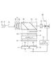
[0015]Jenningsらによる上記参照された出願に説明されている装置の一実施形態が図1の概略的正投影図に図示されている。2次元走査用の構台(gantry)構造10は、1対の固定パラレルレール12、14を含んでいる。2つのパラレル構台ビーム16、18は、固定レール12、14から離れて、かつこれにサポートされている設定距離において共に固定され、図示されていないモータと、固定レール12、14に沿ってローラやボール軸受上をスライドするドライブ機構とによってコントロールされる。ビームソース20は構台ビーム16、18にスライド可能にサポートされており、図示されていないモータと、これらに沿ってスライドするドライブ機構とによってコントロールされるビーム16、18の下方に吊るされることがある。シリコンウェーハ22や他の基板は構台構造10の下方に静止してサポートされる。ビームソース20は、レーザ光ソースと、ウェーハ22に衝突する下方ファン形状ビーム24を、従来低速方向と称される固定レール12、14に略平行に延びるラインビーム26として生成するための光学部品とを含んでいる。本明細書に図示されていないが、構台構造はさらに、ファン形状ビーム24に略平行な方向にレーザ光ソースおよび光学部品を移動させるためのZ軸ステージを含んでいるため、ビームソース20とウェーハ22間の距離をコントロール可能に変更させることができ、したがってウェーハ22に対するラインビーム26の焦点合わせをコントロールすることができる。ラインビーム26の例示的な寸法は長さ1cmかつ幅66ミクロンであり、例示的な電力密度は220kW/cm2である。代替的に、ビームソースおよび関連光学部品は静止していてもよいのに対して、ウェーハは、2次元に走査するステージ上にサポートされる。
[0015] One embodiment of the apparatus described in the above referenced application by Jennings et al. Is illustrated in the schematic orthographic view of FIG. The two-dimensional
[0016]通常の動作において、構台ビーム16、18は固定レール12、14に沿った特定の位置に設定され、ビームソース20は構台ビーム16、18に沿って均一な速度で移動されて、従来高速方向と称される方向の長い寸法に直交するラインビーム26を走査する。したがって、ラインビーム26は、ウェーハ22の一方の側から他方に走査されて、ウェーハ22の1cm範囲を照射する。ラインビーム26は十分狭く、高速方向の走査速度は、ウェーハの特定のエリアがラインビーム26の光学放射に瞬間的にだけ暴露される程度高速であるが、ラインビームのピークの強度は、表面領域を極めて高い温度に加熱するのに十分である。しかしながら、ウェーハ22のより深い部分はそれほど加熱されず、さらに表面領域を迅速に冷却するためのヒートシンクとして作用する。高速走査が完了されると、ラインビーム26が、低速軸に沿って延びる長い寸法に沿って移動されるように、構台ビーム16、18は固定レール12、14に沿って新たな位置に移動される。次いで高速走査が実行されて、ウェーハ22の近接する範囲を照射する。ウェーハ22全体が熱処理されるまで、交互の高速および低速走査が、恐らくビームソース20の蛇行経路で反復される。
[0016] In normal operation, the
[0017]光学ビームソース20はレーザアレイを含んでいる。一例が図2および図3に正投影的に図示されており、ここで約810nmのレーザ放射が2つのレーザバースタック32から光学システム30に生成され、このうちの一方が図4の端面図に図示されている。各レーザバースタック32は、GaAs半導体構造の垂直p−n接合に一般的に対応し、横方向に約1cm延び、かつ約0.9mmで分離されている14個のパラレルバー34を含んでいる。通常、水冷却層はバー34間に配置される。49個のエミッタ36が各バー34に形成され、各々は、直交方向に異なる発散角を有するそれぞれのビームを発する個別GaAsレーザを構成する。図示されているバー34は、長い寸法が多くのエミッタ36に対して延びるように位置決めされ、低速軸に沿って整列され、この短い寸法は高速軸に沿って整列された1ミクロン未満のp−n空乏層に対応する。高速軸に沿った小型ソースサイズは高速軸に沿った効果的なコリメーションを許容する。発散角は高速軸に沿って大きく、低速軸に沿っては比較的小さい。
[0017] The
[0018]図2および図3に戻ると、2つの円筒形小型レンズアレイ40がレーザバー34に沿って位置決めされ、高速軸に沿って狭ビームのレーザ光をコリメートする。これらは接着剤によってレーザスタック32に固着され、発光エリア36に延びるようにバー34と整列されてもよい。
[0018] Returning to FIGS. 2 and 3, two
[0019]光学ビームソース20はさらに従来の光学要素を含むことができる。当業者によるこのような要素の選択はこのような例に制限されないが、このような従来の光学要素は、インタリーバおよび偏光マルチプレクサを含むことができる。図2および3の実施例において、2つのバースタック32からの2セットのビームがインタリーバ42に入力され、これは、多ビームスプリッタータイプの構造を有しており、2つの内部斜面、例えば光を選択的に反射および透過させる反射パラレルバンド上に特殊コーティングを有している。このようなインタリーバはResearch Electro Optics(REO)から市販されている。インタリーバ42において、バー34からスタック32の一方の側へビームが代替的に反射または透過されることによって、対応する選択的な透過/反射を経るバー34からのビームとスタック32のもう一方の側でインタリーブされて、個別エミッタ36から他の方法で間隔をあけられた放射プロファイルを充填することができるように、パターン化金属反射バンドが、2つのバースタック32から1セットのビームごとに角度付き表面に形成される。
[0019] The
[0020]第1のセットのインタリーブビームが4分の1波長板48を通過して、第2のセットのインタリーブビームに対してその偏光を回転させる。両セットのインタリーブビームは、ダブル偏光ビームスプリッタの構造を有する偏光マルチプレクサ(PMUX)52に入力される。このようなPMUXはResearch Electro Opticsから市販されている。第1の対角インタフェース層54および第2の対角インタフェース層56によって2つのセットのインタリーブビームは、その前面から共通軸に沿って反射される。第1のインタフェース54は通常、ハードリフレクタ(HR)として設計された誘電干渉フィルタとして実現されるのに対して、第2のインタフェース56はレーザ波長で偏光ビームスプリッタ(PBS)として設計された誘電干渉フィルタとして実現される。結果として、第1のインタフェース層54から反射された第1のセットのインタリーブビームは第2のインタフェース層56の背面に衝突する。4分の1波長板48によって導入された偏光回転ゆえに、第1のセットのインタリーブビームは第2のインタフェース層56を通過する。PMUX52によって出力されたソースビーム58の強度は、2つのセットのインタリーブビームのどちらかの強度から倍増される。
[0020] The first set of interleaved beams passes through the
[0021]図面において個別に示されているが、インタリーバ42、4分の1波長板48およびPMUX52およびこのインタフェース54、56、ならびに入力および出力面に取り付けられることがある追加フィルタは通常、UV硬化性エポキシなどのプラスチックカプセル材料によって共に接合されて、剛性光学システムを提供する。重要なインタフェースは、レーザスタック32への小型レンズ40のプラスチック固着であり、この上でこれらはバー34に整列されなければならない。ソースビーム58は1セットの円筒形レンズ62、64、66を通過して、低速軸に沿ってソースビーム58に焦点に合わせる。
[0021] Although shown separately in the drawings, the
[0022]1次元光パイプ70は低速軸に沿ってソースビームを均質化する。円筒形レンズ62、64、66によって焦点を合わされたソースビームは光パイプ70に入り、有限発散角は低速軸に沿っているが、実質的には高速軸に沿ってコリメートされている。図5の正投影図により明確に図示されている光パイプ70はビームホモゲナイザーとて作用し、低速軸上で間隔をあけられているバースタック32において多くのエミッタ36によって導入された低速軸に沿ってビーム構造を減らす。光パイプ70は、全内部反射を減らすためにかなり高い屈折率を有する光学ガラスの矩形スラブ72として実現されてもよい。これは低速軸に沿った短い寸法と、高速軸に沿った長い寸法とを有している。スラブ72は、入力面76上の低速軸に沿って収束するソースビーム58の軸74に沿って実質的な距離を延びている。ソースビーム58は、スラブ72の上部および底部表面から数回内部反射されることによって、低速軸に沿ってテクスチャリングの多くを除去することができ、かつ、これが出力面78に延びる場合に低速軸に沿ってビームを均質化することができる。しかしながら、ソースビーム58はすでに、高速軸に沿って(円筒形小型レンズ40によって)十分コリメートされ、スラブ72は、ソースビーム58がスラブ72のサイド表面に内部反射されないが、高速軸に沿ってそのコリメーションを維持するのに十分幅広いものである。光パイプ70は、出入りアパーチャとビームの収束および発散をコントロールするために軸方向に沿って先細りされてもよい。1次元光パイプは代替的に、スラブ72の上面および下面に一般的に対応する2つの平行反射表面として実現可能であり、ソースビームはこれらの間を通過する。
[0022] A one-
[0023]光パイプ70によって出力されたソースビームは一般的に均一である。図6の概略図にさらに図示されているように、さらなるアナモルフィックレンズセット、つまり光学部品80、82は低速軸において出力ビームを拡大させ、またウェーハ22上に所望のラインビーム26を投影するために略球状レンズを含んでいる。アナモルフィック光学部品80、82はソースビームを2次元に成形し、制限長の狭ラインビームを生成する。高速軸の方向において、(システムは有限ソース共役によって設計されてもよいよいが)出力光学部品は、光パイプの出力のソースの無限共役と、ウェーハ22の結像平面の有限共役とを有しているのに対して、低速軸の方向においては、出力光学部品は、光パイプ70の出力におけるソースの有限共役と、結像平面の有限共役とを有している。さらに、低速軸の方向において、レーザバーの多くのレーザダイオードからの不均一放射は光パイプ70によって均質化される。光パイプ70の均質化能力は、光が光パイプ70を横切って反射される回数に大きく左右される。この回数は、光パイプ70の長さ、もしあれば先細りの方向、出入りアパーチャのサイズならびに光パイプ70への発射角によって判断される。さらなるアナモルフィック光学部品は、ウェーハ22の表面上の所望の寸法のラインビームにソースビームの焦点を合わせる。
[0023] The source beam output by the
[0024]RTPおよび他のタイプの放射熱処理に関して頻発する問題は、熱処理されるウェーハの温度を監視することである。ウェーハに結合された光量はウェーハにすでに形成されている表面構造に大きく左右されるために、温度測定が望まれる。さらに、光ソース条件はわずかに変更することがある。広角高温計が、ウェーハの大部分を監視するために一般的にRTPと併用される。このような高温計は、常時ウェーハの小エリアのみを照射するフォーカスレーザビームについては一般的に不適切であり、ウェーハのバルクを環境温度付近のままにする。 [0024] A frequent problem with RTP and other types of radiant heat treatment is to monitor the temperature of the wafer being heat treated. Temperature measurement is desired because the amount of light coupled to the wafer is highly dependent on the surface structure already formed on the wafer. Furthermore, the light source conditions may change slightly. Wide angle pyrometers are commonly used with RTP to monitor the majority of the wafer. Such pyrometers are generally inadequate for focused laser beams that irradiate only a small area of the wafer at all times and leave the bulk of the wafer near ambient temperature.
[0025]本発明の一態様は、フォトダイオードなどの光学検出器61と、レーザ放射の波長、例えば810nmをブロックする光学フィルタ63とを含む、図6に概略的に図示された、レーザソース光の焦点をウェーハに合わせて、ウェーハ22上のラインビーム26の近接部分から発せられた熱放射をリバース方向の高温計60に向けるのに使用される同じ光学部品を使用する。高温計フィルタ63は好ましくは、対象温度で迅速に変化するPlankian黒体放射曲線の領域にセンタリングされた狭通過帯域フィルタである。好ましい高温計通過帯域は1550nmでセンタリングされる(この場合、検出器61はInGaAsフォトダイオードであってもよい)。多数の代替例のうちの1つとして、高温計通過帯域は950nmにセンタリングされてもよい(この場合、検出器61はSiフォトダイオードであってもよい)。通過帯域は、短い波長では数十nmにわたって、長い波長では恐らく100nmにわたって延びることがある。光学部品は一般的に反転性であるため、リバース方向においてラインビーム26上、またはこれに極めて近いウェーハ22の小エリアのみを検出して、あるサイズのバースタックの発光面を一般的に有しているエリアにその画像を光学的に拡大する。小レーザビームアニーリングによって、ラインビーム26の直近の近接部分においても表面層温度の相当な変化があるが、Plankian黒体スペクトルの性質によって、最も熱いエリアは熱発光放射を決定付ける(dominate)。通常、810nmのレーザ波長を桁違いにブロックし、かつ高温計波長からレーザ自然発光を実質的にブロックする1550nmまたは950nm付近の通過帯域を有する狭バンド干渉フィルタ63が使用される。2つのPMUXインタフェース54、56は、その偏光に関係なく高温計波長を通過させるように設計されている。このような機能は、高温計波長ではなく810nmソース放射にチューニングされた干渉ミラーによって実現可能である。第1のインタフェース54はハードリフレクタ(HR)干渉フィルタであるが、第2のインタフェース56は、810nmまたは他のレーザ波長にチューニングされた偏光ビームスプリッタ(PBS)であるように、従来のインタフェース54、56は設計される。本発明について、PBSインタフェース56での干渉フィルタは、レーザ光の第1の偏光(またはこの少なくとも大部分)を反射しつつ高温計波長での第1の偏光の実質的部分(例えば、72%)を通過させる程度にデチューンされる。同様に、HRインタフェース54での干渉フィルタは、両波長の他の偏光の大部分を反射しつつ高温計波長での第1の偏光の大部分(例えば、90%)を通過させるように再設計される。PMUXインタフェース54、56および狭バンド高温計フィルタ63の両方のフィルタリングの結果として、光検出器61は熱(黒体放射)スペクトルの一部における狭バンド光学信号のみを受信する。従って、本発明において特定の波長をブロックまたは許容する光学フィルタまたは経路は、たとえその波長の光のすべてを完全にブロックまたは完全に許容するとしても十分である。
[0025] One aspect of the present invention includes laser source light, schematically illustrated in FIG. 6, including an
[0026]光検出器61の出力はソースコントローラ65に供給され、これは検出された光電流をウェーハ温度に変換して、これを所望の温度と比較することによって、レーザバー32に供給された電力を調整して、所望のウェーハ温度の方向においてその光学出力を増減させる。
[0026] The output of the
[0027]この手法の難しさは、GaAsや他の半導体レーザが、通常高温計波長に重畳する低レベル自然発光のかなり広いスペクトルを有していることである。高温計フィルタ63が高温計波長でブロックしない自然発光の結果として、光検出器61は、追加フィルタリングなしで、(a)高温計波長でのウェーハ黒体放射と、(b)高温計波長でのレーザソース自然発光の一部の両方を検出するであろう。
[0027] The difficulty with this approach is that GaAs and other semiconductor lasers have a fairly broad spectrum of low-level spontaneous emission that usually overlaps the pyrometer wavelength. As a result of spontaneous light emission where the
[0028]高温計性能は、バースタック32とインタリーバ42との間に置かれたノッチフィルタ67、またはインタリーバ42とPMUX52との間に置かれたノッチフィルタ68によって高温計波長でのレーザソース自然放射を取り除くことによって大きく改良可能である。ノッチフィルタ67または68は、具体的にはいずれの波長、例えば1550nmまたは950nmが高温計フィルタ63によって通過されても高温計波長でソース放射をブロックし、少なくとも810nmのレーザ放射を通過させる。高温計波長の透過係数に対するレーザ波長の透過係数の比は桁違いであるはずである。フィルタ67、68の最低限の要件は、短い波長での放射が高温計を本質的に劣化させずに、これらがレーザ波長よりも長い波長、例えば810nmをブロックすることである。ノッチフィルタ67、68は、スタンドアローンフィルタとして実現されてもよいが、インタリーバ42またはPMUX52のいずれかにコーティングされた干渉フィルタとして容易に実現されてもよい。
[0028] The pyrometer performance is measured by the natural radiation of the laser source at the pyrometer wavelength by a
[0029]図7の断面図に図示された、第1のノッチフィルタ67の好都合な形態は、各レーザスタック32が置かれ、かつ小型レンズ40が発光エリア36にわたるレーザスタックに接着剤によって固着されているハウジング79を含んでいる。小型レンズ40は、略コリメートビームを生成するために図面に直交して延びるレーザバー34に沿って延びる小型円筒形レンズである。ハウジング79の上部は、高温計フィルタ67に対応する干渉フィルタ84が高温計波長を選択的に反映し、かつレーザ波長を通過させるように形成されたInfrasil(光学石英)のフラットウィンドウつまりウィンドウスラブ83によってシールされている。レーザ放射に対する反射防止コーティングがウィンドウ83の片面または両面に形成されてもよい。シールされた構造は、小型レンズ40がレーザスタック32から剥がれ、かつ不整合がレーザソースにおける熱逃走をもたらしても、有機汚染がハウジングの内部に制限され、下流光学部品に影響しないという利点を有している。
[0029] An advantageous form of the
[0030]しかしながら、反射放射は、加熱およびモードホッピングの両方ゆえにレーザバーでの問題を生成する。この問題を解決するために、ハウジングの壁86、88は一定でない高さを有しており、ウィンドウ83および取り付けられたフィルタ84は、入射ビーム81に直交する平面に対して約1°または他の適切な角度で傾斜される。結果として、高温計波長の反射放射は、発光エリア間、つまりスタックバー34間のゾーンにおいてレーザスタック32に衝突する反射ビーム90の斜角で反射される。これによって放射はレーザ構造に結合されない。傾斜ウィンドウ83のさらなる利点は、任意の反射レーザ放射はまた発光エリア36から偏向されることである。さらに、バー34間のバースタックの層は、通常、水冷却チャネル(図示せず)を含有しているため、反射放射の熱エネルギーは即座に吸収される。ハウジング79およびシールウィンドウ83は十分に不透過性の構造を構成すべきであるため、不具合に起因する任意の蒸発残渣が、不具合を検出して、レーザスタック32への電力を除去するのに十分な時間の間構造内に閉じ込められる。
[0030] However, reflected radiation creates problems with laser bars because of both heating and mode hopping. To solve this problem, the
[0031]図8の断面図に図示されている代替構造は高温計フィルタ84を、シールされたハウジング内の傾斜ウィンドウ83の底部に置くため、この不具合もまたハウジング79の内側に閉じ込められる。図9の断面図に図示されたさらなる代替構造は等しい高さのハウジング側壁86、88を有している。楔形ウィンドウ92は側壁86、88の上に平らにあるが、高温計フィルタ84は、楔ウィンドウ92の上面の発光ビーム81に対して傾斜される。
[0031] The alternative structure illustrated in the cross-sectional view of FIG. 8 places the
[0032]光学ソースとウェーハ間のアナモルフィック光学部品は、通常、反射防止コーティングを含んでいる。本発明によって、反射防止および他のコーティングは、レーザ波長だけではなく高温計波長に対しても設計される必要がある。 [0032] Anamorphic optics between the optical source and the wafer typically include an anti-reflective coating. According to the present invention, antireflection and other coatings need to be designed not only for the laser wavelength but also for the pyrometer wavelength.
[0033]本発明は走査済みラインビームについて説明されてきたが、これはまた、基板の隣接する部分を順次照射するパルスレーザシステムに適用されてもよい。しかしながら、CW走査動作は、高温計の観点から時間的に不変の温度である走査済み領域によって高温計がイメージングされる点において好都合である。 [0033] Although the present invention has been described with respect to a scanned line beam, it may also be applied to a pulsed laser system that sequentially illuminates adjacent portions of a substrate. However, the CW scanning operation is advantageous in that the pyrometer is imaged by a scanned region that is a time-invariant temperature from a pyrometer perspective.
[0034]システム全体の何らかの再設計によって、PMUXインタフェースによって実行される波長フィルタリングは、レーザ波長での選択透過および高温計波長での選択反射と置換可能である。インタリーバ42または偏向マルチプレクサ52のいずれかなしで、またはこれらの両方なしで本発明を実施することができる。考えられる一例として、反射表面54、56に類似の(またはこれらのうちの1つに類似の)光学要素が、本発明を実施するのに用いられてもよく、この要素は偏向マルチプレクサの一部ではない。
[0034] With some redesign of the entire system, the wavelength filtering performed by the PMUX interface can be replaced with selective transmission at the laser wavelength and selective reflection at the pyrometer wavelength. The present invention may be practiced without either the
[0035]本発明は好ましい実施形態を具体的に参照して詳細に説明されてきたが、この変形および修正が、本発明の主旨および範囲を逸脱せずになされてもよいことが理解される。 [0035] Although the invention has been described in detail with particular reference to the preferred embodiments, it will be understood that variations and modifications can be made without departing from the spirit and scope of the invention. .
22…ウェーハ、26…ラインビーム、40…小型レンズ、42…インタリーバ、52…PMUX、54、56…PMUXインタフェース、60…高温計、61…光学検出器、63…光学フィルタ、65…ソースコントローラ、67、68…ノッチフィルタ、79…ハウジング、81…入射ビーム、83…ウィンドウスラブ、84…干渉フィルタ、86、88…壁、92…楔形ウィンドウ 22 ... Wafer, 26 ... Line beam, 40 ... Small lens, 42 ... Interleaver, 52 ... PMUX, 54, 56 ... PMUX interface, 60 ... Pyrometer, 61 ... Optical detector, 63 ... Optical filter, 65 ... Source controller, 67, 68 ... notch filter, 79 ... housing, 81 ... incident beam, 83 ... window slab, 84 ... interference filter, 86, 88 ... wall, 92 ... wedge-shaped window
Claims (10)
前記半導体材料により熱として吸収されるレーザ波長のレーザ光を生成するステップと、
前記レーザ光から、該レーザ光により加熱された場合に前記半導体材料が黒体放射する高温計波長域をフィルタリングするステップと、
前記レーザ波長において反射し前記高温計波長域において透過するビームスプリッタに前記レーザ光を通すステップと、
前記ビームスプリッタで反射した前記レーザ光の焦点を、前記ウェーハの径のわずかな範囲である狭域幅のラインビームに合わせるステップと、
加熱時間と、前記ラインビームの狭域幅に対応する前記ウェーハの限られた表面領域の深さとを制限するのに十分な特定の走査速度で、該ウェーハの表面を横断して前記ラインビームを走査することで、絶えず動いている該表面領域を該加熱時間の間約1000℃の特定の温度まで加熱するステップと、
前記ウェーハの前記移動表面領域から発するウェーハ放射ビームを提供するために、前記ラインビームにより照射された該ウェーハの移動表面領域を前記ビームスプリッタに結像するステップと、
前記高温計波長域内にある前記ウェーハ放射の一部を、前記ビームスプリッタを介して、該高温計波長域の範囲内で反応する光学検出器に通すステップと、
を含み、
前記レーザ光が個別のレーザエミッタのアレイにより生成され、
前記レーザ光から前記高温計波長域をフィルタリングするステップが、該高温計波長域の範囲内にあるレーザ光の一部を、前記エミッタのうち隣接するもの同士の間の領域に反射させるステップを含む、
方法。A method of heating a wafer of semiconductor material,
Generating laser light of a laser wavelength that is absorbed as heat by the semiconductor material;
Filtering the pyrometer wavelength region from which the semiconductor material emits a black body when heated by the laser light from the laser light;
Passing the laser light through a beam splitter that reflects at the laser wavelength and transmits at the pyrometer wavelength range;
Focusing the laser beam reflected by the beam splitter with a narrow line beam that is a small range of the diameter of the wafer;
The line beam is traversed across the surface of the wafer at a specific scan rate sufficient to limit the heating time and the depth of the limited surface area of the wafer corresponding to the narrow width of the line beam. Heating the constantly moving surface area to a specific temperature of about 1000 ° C. during the heating time by scanning;
Imaging the moving surface area of the wafer irradiated by the line beam onto the beam splitter to provide a wafer radiation beam emanating from the moving surface area of the wafer;
Passing a portion of the wafer radiation within the pyrometer wavelength range through the beam splitter to an optical detector that reacts within the pyrometer wavelength range;
Only including,
The laser light is generated by an array of individual laser emitters;
Filtering the pyrometer wavelength region from the laser light includes reflecting a portion of the laser light within the pyrometer wavelength region to a region between adjacent ones of the emitters. ,
Method.
請求項3に記載の方法。The step of focusing the laser beam on the line beam and the step of imaging include passing the laser beam in a first forward direction through the optical path of the common optical device; and passing the wafer radiation to the optical path. Passing in the opposite direction through
The method of claim 3 .
前記レーザ光が、電力密度が約220kW/cm2である光ビームを含む、
請求項1に記載の方法。The narrow width of the line beam is about 66 microns;
The laser beam includes a light beam having a power density of about 220 kW / cm 2 ;
The method of claim 1.
前記半導体材料が放射光を熱として吸収するレーザ波長でレーザ光を放射するレーザ光ソースと、
前記レーザ波長では放射光を反射し高温計波長では放射光を通すように調整された反射面と、
前記ウェーハに焦点が合わされ前記反射面と前記ウェーハとの間に配置された光ラインビーム出力パターン、を有する光学部品と、
前記ラインビームに直交する速軸を有するラインビーム走査装置と、
前記光学部品と向かい合う前記反射面側に配置されて、前記ラインビームにより照射された前記ウェーハの領域の像を受け付ける高温計であって、前記高温計波長に反応する高温計と、
前記レーザ光ソースと前記反射面との間に配置され、前記レーザ光ソースにより発せられた、前記高温計波長を含む放射光の一部を遮断する第1光学フィルタと、
を備え、
前記レーザ光ソースがレーザエミッタアレイを備え、
前記第1光学フィルタが、前記アレイに対して傾斜していることで前記エミッタのうち隣接するもの同士の間の領域に前記高温計波長の光を反射する反射面を備える、
システム。A system for heat-treating a semiconductor material wafer,
A laser light source that emits laser light at a laser wavelength at which the semiconductor material absorbs the emitted light as heat; and
A reflective surface adjusted to reflect the emitted light at the laser wavelength and to pass the emitted light at the pyrometer wavelength;
An optical component having an optical line beam output pattern focused on the wafer and disposed between the reflective surface and the wafer;
A line beam scanning device having a fast axis perpendicular to the line beam;
A pyrometer disposed on the reflective surface facing the optical component and receiving an image of the area of the wafer irradiated by the line beam, the pyrometer being responsive to the pyrometer wavelength;
A first optical filter disposed between the laser light source and the reflecting surface and blocking a part of the emitted light including the pyrometer wavelength emitted by the laser light source;
Equipped with a,
The laser light source comprises a laser emitter array;
The first optical filter includes a reflecting surface that reflects light of the pyrometer wavelength in a region between adjacent ones of the emitters by being inclined with respect to the array.
system.
請求項9に記載のシステム。The pyrometer includes a photodetector and a second optical filter that passes the pyrometer wavelength and does not pass the laser wavelength.
The system according to claim 9 .
Applications Claiming Priority (5)
| Application Number | Priority Date | Filing Date | Title |
|---|---|---|---|
| US62752704P | 2004-11-12 | 2004-11-12 | |
| US60/627,527 | 2004-11-12 | ||
| US11/195,380 | 2005-08-02 | ||
| US11/195,380 US7438468B2 (en) | 2004-11-12 | 2005-08-02 | Multiple band pass filtering for pyrometry in laser based annealing systems |
| PCT/US2005/036796 WO2006055130A2 (en) | 2004-11-12 | 2005-10-12 | Multiple band pass filtering for pyrometry in laser based annealing systems |
Publications (3)
| Publication Number | Publication Date |
|---|---|
| JP2008520096A JP2008520096A (en) | 2008-06-12 |
| JP2008520096A5 JP2008520096A5 (en) | 2008-11-06 |
| JP5103186B2 true JP5103186B2 (en) | 2012-12-19 |
Family
ID=35695702
Family Applications (1)
| Application Number | Title | Priority Date | Filing Date |
|---|---|---|---|
| JP2007541192A Active JP5103186B2 (en) | 2004-11-12 | 2005-10-12 | Multi-band pass filtering for high temperature measurements in laser-based annealing systems |
Country Status (6)
| Country | Link |
|---|---|
| US (2) | US7438468B2 (en) |
| EP (1) | EP1831658B1 (en) |
| JP (1) | JP5103186B2 (en) |
| KR (1) | KR101226634B1 (en) |
| CN (1) | CN101065649B (en) |
| WO (1) | WO2006055130A2 (en) |
Families Citing this family (40)
| Publication number | Priority date | Publication date | Assignee | Title |
|---|---|---|---|---|
| US6987240B2 (en) * | 2002-04-18 | 2006-01-17 | Applied Materials, Inc. | Thermal flux processing by scanning |
| US7910499B2 (en) * | 2004-11-12 | 2011-03-22 | Applied Materials, Inc. | Autofocus for high power laser diode based annealing system |
| US7422988B2 (en) | 2004-11-12 | 2008-09-09 | Applied Materials, Inc. | Rapid detection of imminent failure in laser thermal processing of a substrate |
| US7438468B2 (en) | 2004-11-12 | 2008-10-21 | Applied Materials, Inc. | Multiple band pass filtering for pyrometry in laser based annealing systems |
| US7569463B2 (en) * | 2006-03-08 | 2009-08-04 | Applied Materials, Inc. | Method of thermal processing structures formed on a substrate |
| US20070291505A1 (en) * | 2006-06-02 | 2007-12-20 | Rance Fortenberry | Light source assembly with integrated optical pipe |
| US7494272B2 (en) * | 2006-06-27 | 2009-02-24 | Applied Materials, Inc. | Dynamic surface annealing using addressable laser array with pyrometry feedback |
| US20080025354A1 (en) * | 2006-07-31 | 2008-01-31 | Dean Jennings | Ultra-Fast Beam Dithering with Surface Acoustic Wave Modulator |
| US7548364B2 (en) | 2006-07-31 | 2009-06-16 | Applied Materials, Inc. | Ultra-fast beam dithering with surface acoustic wave modulator |
| US7674999B2 (en) | 2006-08-23 | 2010-03-09 | Applied Materials, Inc. | Fast axis beam profile shaping by collimation lenslets for high power laser diode based annealing system |
| US7659187B2 (en) | 2006-11-03 | 2010-02-09 | Applied Materials, Inc. | Method of forming PN junctions including a post-ion implant dynamic surface anneal process with minimum interface trap density at the gate insulator-silicon interface |
| US7804042B2 (en) * | 2007-06-18 | 2010-09-28 | Applied Materials, Inc. | Pryometer for laser annealing system compatible with amorphous carbon optical absorber layer |
| US8148663B2 (en) | 2007-07-31 | 2012-04-03 | Applied Materials, Inc. | Apparatus and method of improving beam shaping and beam homogenization |
| US8674257B2 (en) | 2008-02-11 | 2014-03-18 | Applied Materials, Inc. | Automatic focus and emissivity measurements for a substrate system |
| US7713757B2 (en) * | 2008-03-14 | 2010-05-11 | Applied Materials, Inc. | Method for measuring dopant concentration during plasma ion implantation |
| US8319149B2 (en) * | 2008-04-16 | 2012-11-27 | Applied Materials, Inc. | Radiant anneal throughput optimization and thermal history minimization by interlacing |
| US7947584B2 (en) * | 2008-05-02 | 2011-05-24 | Applied Materials, Inc. | Suitably short wavelength light for laser annealing of silicon in DSA type systems |
| US8434937B2 (en) | 2008-05-30 | 2013-05-07 | Applied Materials, Inc. | Method and apparatus for detecting the substrate temperature in a laser anneal system |
| US9089928B2 (en) | 2008-08-20 | 2015-07-28 | Foro Energy, Inc. | Laser systems and methods for the removal of structures |
| US11590606B2 (en) * | 2008-08-20 | 2023-02-28 | Foro Energy, Inc. | High power laser tunneling mining and construction equipment and methods of use |
| US9719302B2 (en) | 2008-08-20 | 2017-08-01 | Foro Energy, Inc. | High power laser perforating and laser fracturing tools and methods of use |
| US9080425B2 (en) | 2008-10-17 | 2015-07-14 | Foro Energy, Inc. | High power laser photo-conversion assemblies, apparatuses and methods of use |
| US9669492B2 (en) | 2008-08-20 | 2017-06-06 | Foro Energy, Inc. | High power laser offshore decommissioning tool, system and methods of use |
| US9664012B2 (en) | 2008-08-20 | 2017-05-30 | Foro Energy, Inc. | High power laser decomissioning of multistring and damaged wells |
| US20120074110A1 (en) * | 2008-08-20 | 2012-03-29 | Zediker Mark S | Fluid laser jets, cutting heads, tools and methods of use |
| US10301912B2 (en) | 2008-08-20 | 2019-05-28 | Foro Energy, Inc. | High power laser flow assurance systems, tools and methods |
| US8254767B2 (en) * | 2008-08-29 | 2012-08-28 | Applied Materials, Inc. | Method and apparatus for extended temperature pyrometry |
| JP5349129B2 (en) * | 2009-05-07 | 2013-11-20 | 住友重機械工業株式会社 | Laser irradiation device |
| JP5537615B2 (en) * | 2011-08-10 | 2014-07-02 | ウルトラテック インク | System and method for forming a time-averaged line image |
| US8946594B2 (en) | 2011-11-04 | 2015-02-03 | Applied Materials, Inc. | Optical design for line generation using microlens array |
| KR101288993B1 (en) * | 2011-12-20 | 2013-08-16 | 삼성디스플레이 주식회사 | Laser annealing device |
| US9028135B1 (en) | 2012-01-12 | 2015-05-12 | United States Of America As Represented By The Administrator Of The National Aeronautics And Space Administration | Pyrometer |
| DE102012020743A1 (en) * | 2012-10-23 | 2014-04-24 | Oerlikon Trading Ag, Trübbach | UV irradiation device for clocked operation |
| US8912495B2 (en) * | 2012-11-21 | 2014-12-16 | Kla-Tencor Corp. | Multi-spectral defect inspection for 3D wafers |
| US9085050B1 (en) | 2013-03-15 | 2015-07-21 | Foro Energy, Inc. | High power laser fluid jets and beam paths using deuterium oxide |
| CN103592713A (en) * | 2013-11-29 | 2014-02-19 | 苏州大学 | Sidelobe-free angle-selection laser filter |
| DE102016223215A1 (en) | 2016-11-23 | 2018-05-24 | Trumpf Laser- Und Systemtechnik Gmbh | Irradiation device and processing machine with it |
| CN106949974B (en) * | 2017-04-11 | 2019-04-05 | 东北林业大学 | The true temperature measurement device of multispectral line temperature and method |
| WO2020222702A1 (en) * | 2019-04-30 | 2020-11-05 | Ams Sensors Singapore Pte. Ltd. | Spectrometer including an illumination channel that includes a light pipe |
| JP7542350B2 (en) * | 2020-07-21 | 2024-08-30 | Jswアクティナシステム株式会社 | Laser annealing apparatus, laser annealing method, and method for manufacturing semiconductor device |
Family Cites Families (75)
| Publication number | Priority date | Publication date | Assignee | Title |
|---|---|---|---|---|
| US3778791A (en) | 1971-10-06 | 1973-12-11 | Nasa | Thermomagnetic recording and magneto-optic playback system having constant intensity laser beam control |
| US4099875A (en) | 1977-02-07 | 1978-07-11 | Sperry Rand Corporation | Coaxial multi-detector system and method for measuring the extinction coefficient of an atmospheric scattering medium |
| US4129780A (en) * | 1977-06-21 | 1978-12-12 | Varo, Inc. | Active imaging system using time programmed dwell |
| US4215275A (en) * | 1977-12-07 | 1980-07-29 | Luxtron Corporation | Optical temperature measurement technique utilizing phosphors |
| US4305640A (en) | 1978-11-24 | 1981-12-15 | National Research Development Corporation | Laser beam annealing diffuser |
| SE420769B (en) * | 1978-12-05 | 1981-10-26 | Asea Ab | FIBEROPTICAL TEMPERATURE METHOD OF PYROMETER TYPE |
| JPS5799747A (en) | 1980-12-12 | 1982-06-21 | Fujitsu Ltd | Light beam diffusor |
| US5231595A (en) * | 1983-06-06 | 1993-07-27 | Minolta Camera Kabushiki Kaisha | Pyrometer |
| JPS605508A (en) * | 1983-06-24 | 1985-01-12 | Agency Of Ind Science & Technol | Manufacture of semiconductor crystal thin film |
| GB2203539B (en) | 1985-02-19 | 1989-08-31 | Atomic Energy Authority Uk | Apparatus for monitoring infra-red emissions |
| US4647774A (en) | 1985-03-04 | 1987-03-03 | Quantum Logic Corporation | Pyrometer #2 |
| JPS62186531A (en) | 1986-02-03 | 1987-08-14 | インタ−ナショナル ビジネス マシ−ンズ コ−ポレ−ション | Method and apparatus for manufacturing integrated circuit structure with smooth boundary surface |
| US4740113A (en) * | 1986-09-25 | 1988-04-26 | Japan Tobacco, Inc. | Receiving/delivering apparatus for rod-shaped objects transported by an air flow |
| JP2664723B2 (en) * | 1988-05-11 | 1997-10-22 | 富士通株式会社 | Laser annealing equipment |
| US5238858A (en) | 1988-10-31 | 1993-08-24 | Sharp Kabushiki Kaisha | Ion implantation method |
| US5007741A (en) * | 1989-09-25 | 1991-04-16 | At&T Bell Laboratories | Methods and apparatus for detecting impurities in semiconductors |
| NL9001200A (en) * | 1990-05-23 | 1991-12-16 | Imec Inter Uni Micro Electr | METHOD AND APPARATUS FOR MEASURING TEMPERATURE RADIATION USING A PYROMETER USING COMPENSATION LAMPS |
| US5508934A (en) * | 1991-05-17 | 1996-04-16 | Texas Instruments Incorporated | Multi-point semiconductor wafer fabrication process temperature control system |
| US5229883A (en) * | 1991-10-28 | 1993-07-20 | Mcdonnell Douglas Corporation | Hybrid binary optics collimation fill optics |
| JP2720744B2 (en) | 1992-12-28 | 1998-03-04 | 三菱電機株式会社 | Laser processing machine |
| DE69312894T2 (en) * | 1992-12-29 | 1998-02-12 | Philips Electronics Nv | Pyrometer with emission meter |
| JPH07134069A (en) * | 1993-11-10 | 1995-05-23 | Hitachi Ltd | Method for monitoring temperature of substrate |
| DE4414391C2 (en) * | 1994-04-26 | 2001-02-01 | Steag Rtp Systems Gmbh | Method for wave vector selective pyrometry in rapid heating systems |
| US5822222A (en) * | 1995-04-05 | 1998-10-13 | New Jersey Institute Of Technology | Multi-wavelength imaging pyrometer |
| GB9508427D0 (en) * | 1995-04-26 | 1995-06-14 | Electrotech Equipments Ltd | Temperature sensing methods and apparatus |
| US6028722A (en) * | 1996-03-08 | 2000-02-22 | Sdl, Inc. | Optical beam reconfiguring device and optical handling system for device utilization |
| GB9624715D0 (en) | 1996-11-28 | 1997-01-15 | Philips Electronics Nv | Electronic device manufacture |
| US5861992A (en) | 1997-06-20 | 1999-01-19 | Creo Products Inc | Microlensing for multiple emitter laser diodes |
| US6240116B1 (en) | 1997-08-14 | 2001-05-29 | Sdl, Inc. | Laser diode array assemblies with optimized brightness conservation |
| US6174081B1 (en) * | 1998-01-30 | 2001-01-16 | The United States Of America As Represented By The Secretary Of The Navy | Specular reflection optical bandgap thermometry |
| WO2000058700A1 (en) | 1999-03-30 | 2000-10-05 | Tokyo Electron Limited | Temperature measuring system |
| US6303411B1 (en) * | 1999-05-03 | 2001-10-16 | Vortek Industries Ltd. | Spatially resolved temperature measurement and irradiance control |
| DE19939750C2 (en) | 1999-08-21 | 2001-08-23 | Laserline Ges Fuer Entwicklung | Optical arrangement for use in a laser diode arrangement and laser diode arrangement with such an optical arrangement |
| JP4040809B2 (en) | 1999-09-22 | 2008-01-30 | 株式会社東芝 | Fine pattern measuring method, fine pattern measuring apparatus, and recording medium recording fine pattern measuring program |
| US6281471B1 (en) | 1999-12-28 | 2001-08-28 | Gsi Lumonics, Inc. | Energy-efficient, laser-based method and system for processing target material |
| US6494371B1 (en) | 2000-03-09 | 2002-12-17 | Coherent, Inc. | Diode-laser light projector for illuminating a linear array of light modulators |
| US6531681B1 (en) | 2000-03-27 | 2003-03-11 | Ultratech Stepper, Inc. | Apparatus having line source of radiant energy for exposing a substrate |
| US6939434B2 (en) | 2000-08-11 | 2005-09-06 | Applied Materials, Inc. | Externally excited torroidal plasma source with magnetic control of ion distribution |
| US6809012B2 (en) | 2001-01-18 | 2004-10-26 | Semiconductor Energy Laboratory Co., Ltd. | Method of making a thin film transistor using laser annealing |
| DE10119599A1 (en) * | 2001-04-21 | 2002-10-31 | Bosch Gmbh Robert | Method for determining temperatures on semiconductor components |
| US6818894B2 (en) * | 2001-04-30 | 2004-11-16 | The Board Of Trustees Of The University Of Illinois | Method and apparatus for characterization of ultrathin silicon oxide films using mirror-enhanced polarized reflectance fourier transform infrared spectroscopy |
| JP2003059858A (en) | 2001-08-09 | 2003-02-28 | Sony Corp | Laser annealing device and method of manufacturing thin film transistor |
| EP1440346A1 (en) | 2001-11-02 | 2004-07-28 | Honeywell International Inc. | Hollow wedge shape light guide for back illumination |
| KR101067901B1 (en) * | 2001-12-26 | 2011-09-28 | 맷슨 테크날러지 캐나다 인코퍼레이티드 | Temperature measurement and heat-treating methods and systems |
| JP4220707B2 (en) * | 2002-02-26 | 2009-02-04 | 浜松ホトニクス株式会社 | Laser processing head |
| US20050063451A1 (en) * | 2002-02-28 | 2005-03-24 | Shin-Etsu Handotai Co., Ltd | Temperature measuring system, heating device using it and production method for semiconductor wafer, heat ray insulating translucent member, visible light reflection membner, exposure system-use reflection mirror and exposure system, and semiconductor device produced by using them and vetical heat treating device |
| US7005601B2 (en) | 2002-04-18 | 2006-02-28 | Applied Materials, Inc. | Thermal flux processing by scanning |
| US6987240B2 (en) | 2002-04-18 | 2006-01-17 | Applied Materials, Inc. | Thermal flux processing by scanning |
| JP4043859B2 (en) * | 2002-06-18 | 2008-02-06 | 浜松ホトニクス株式会社 | Resin welding apparatus and resin welding method |
| JP2004146782A (en) | 2002-08-29 | 2004-05-20 | Advanced Lcd Technologies Development Center Co Ltd | In-situ monitoring method in crystallization state |
| US20040263986A1 (en) | 2002-09-30 | 2004-12-30 | Brown Daniel M. | Method and device for combining and shaping beams |
| US6847457B2 (en) * | 2002-10-29 | 2005-01-25 | Mitutoyo Corporation | Interferometer using integrated imaging array and high-density phase-shifting array |
| US6747245B2 (en) | 2002-11-06 | 2004-06-08 | Ultratech Stepper, Inc. | Laser scanning apparatus and methods for thermal processing |
| US7095026B2 (en) * | 2002-11-08 | 2006-08-22 | L-3 Communications Cincinnati Electronics Corporation | Methods and apparatuses for selectively limiting undesired radiation |
| US6763054B2 (en) | 2002-11-19 | 2004-07-13 | The Boeing Company | Optical system for improving the brightness of a stack of lensed diode lasers |
| GB2399971B (en) * | 2003-01-22 | 2006-07-12 | Proneta Ltd | Imaging sensor optical system |
| US7327916B2 (en) | 2003-03-11 | 2008-02-05 | Semiconductor Energy Laboratory Co., Ltd. | Beam Homogenizer, laser irradiation apparatus, and method of manufacturing a semiconductor device |
| JP4449316B2 (en) * | 2003-03-18 | 2010-04-14 | パナソニック株式会社 | Semiconductor laser device |
| JP4373115B2 (en) | 2003-04-04 | 2009-11-25 | 株式会社半導体エネルギー研究所 | Method for manufacturing semiconductor device |
| EP1665778A2 (en) * | 2003-08-26 | 2006-06-07 | Redshift Systems Corporation | Infrared camera system |
| US7209624B2 (en) | 2004-01-28 | 2007-04-24 | Eastman Kodak Company | Apparatus and method for illumination of light valves |
| JP4242810B2 (en) | 2004-07-07 | 2009-03-25 | オリンパス株式会社 | Light guide member, lighting device, projector |
| US7910499B2 (en) | 2004-11-12 | 2011-03-22 | Applied Materials, Inc. | Autofocus for high power laser diode based annealing system |
| US7422988B2 (en) * | 2004-11-12 | 2008-09-09 | Applied Materials, Inc. | Rapid detection of imminent failure in laser thermal processing of a substrate |
| US7438468B2 (en) | 2004-11-12 | 2008-10-21 | Applied Materials, Inc. | Multiple band pass filtering for pyrometry in laser based annealing systems |
| US7129440B2 (en) | 2004-11-12 | 2006-10-31 | Applied Materials, Inc. | Single axis light pipe for homogenizing slow axis of illumination systems based on laser diodes |
| US7750266B2 (en) * | 2004-11-17 | 2010-07-06 | Metal Improvement Company Llc | Active beam delivery system for laser peening and laser peening method |
| US7135392B1 (en) | 2005-07-20 | 2006-11-14 | Applied Materials, Inc. | Thermal flux laser annealing for ion implantation of semiconductor P-N junctions |
| US7335611B2 (en) * | 2005-08-08 | 2008-02-26 | Applied Materials, Inc. | Copper conductor annealing process employing high speed optical annealing with a low temperature-deposited optical absorber layer |
| US7684039B2 (en) * | 2005-11-18 | 2010-03-23 | Kla-Tencor Technologies Corporation | Overlay metrology using the near infra-red spectral range |
| US7494272B2 (en) * | 2006-06-27 | 2009-02-24 | Applied Materials, Inc. | Dynamic surface annealing using addressable laser array with pyrometry feedback |
| US8104951B2 (en) * | 2006-07-31 | 2012-01-31 | Applied Materials, Inc. | Temperature uniformity measurements during rapid thermal processing |
| US7674999B2 (en) * | 2006-08-23 | 2010-03-09 | Applied Materials, Inc. | Fast axis beam profile shaping by collimation lenslets for high power laser diode based annealing system |
| US8674257B2 (en) * | 2008-02-11 | 2014-03-18 | Applied Materials, Inc. | Automatic focus and emissivity measurements for a substrate system |
| US8434937B2 (en) * | 2008-05-30 | 2013-05-07 | Applied Materials, Inc. | Method and apparatus for detecting the substrate temperature in a laser anneal system |
-
2005
- 2005-08-02 US US11/195,380 patent/US7438468B2/en active Active
- 2005-10-12 JP JP2007541192A patent/JP5103186B2/en active Active
- 2005-10-12 EP EP05809879.9A patent/EP1831658B1/en not_active Ceased
- 2005-10-12 WO PCT/US2005/036796 patent/WO2006055130A2/en active Application Filing
- 2005-10-12 KR KR1020077012613A patent/KR101226634B1/en active IP Right Grant
- 2005-10-12 CN CN2005800402899A patent/CN101065649B/en active Active
-
2008
- 2008-09-12 US US12/283,615 patent/US7717617B2/en active Active
Also Published As
| Publication number | Publication date |
|---|---|
| WO2006055130A3 (en) | 2006-07-13 |
| EP1831658B1 (en) | 2016-08-03 |
| WO2006055130A2 (en) | 2006-05-26 |
| CN101065649B (en) | 2012-11-28 |
| EP1831658A2 (en) | 2007-09-12 |
| US20090084986A1 (en) | 2009-04-02 |
| KR20070085742A (en) | 2007-08-27 |
| US7438468B2 (en) | 2008-10-21 |
| US7717617B2 (en) | 2010-05-18 |
| CN101065649A (en) | 2007-10-31 |
| JP2008520096A (en) | 2008-06-12 |
| US20060102607A1 (en) | 2006-05-18 |
| KR101226634B1 (en) | 2013-01-25 |
Similar Documents
| Publication | Publication Date | Title |
|---|---|---|
| JP5103186B2 (en) | Multi-band pass filtering for high temperature measurements in laser-based annealing systems | |
| US7422988B2 (en) | Rapid detection of imminent failure in laser thermal processing of a substrate | |
| US7494272B2 (en) | Dynamic surface annealing using addressable laser array with pyrometry feedback | |
| US7804042B2 (en) | Pryometer for laser annealing system compatible with amorphous carbon optical absorber layer | |
| KR101150001B1 (en) | Autofocus for high power laser diode based annealing system | |
| US7129440B2 (en) | Single axis light pipe for homogenizing slow axis of illumination systems based on laser diodes |
Legal Events
| Date | Code | Title | Description |
|---|---|---|---|
| A521 | Request for written amendment filed |
Free format text: JAPANESE INTERMEDIATE CODE: A523 Effective date: 20080910 |
|
| A621 | Written request for application examination |
Free format text: JAPANESE INTERMEDIATE CODE: A621 Effective date: 20080910 |
|
| RD03 | Notification of appointment of power of attorney |
Free format text: JAPANESE INTERMEDIATE CODE: A7423 Effective date: 20101130 |
|
| RD04 | Notification of resignation of power of attorney |
Free format text: JAPANESE INTERMEDIATE CODE: A7424 Effective date: 20101210 |
|
| A977 | Report on retrieval |
Free format text: JAPANESE INTERMEDIATE CODE: A971007 Effective date: 20120308 |
|
| A131 | Notification of reasons for refusal |
Free format text: JAPANESE INTERMEDIATE CODE: A131 Effective date: 20120321 |
|
| A521 | Request for written amendment filed |
Free format text: JAPANESE INTERMEDIATE CODE: A523 Effective date: 20120613 |
|
| TRDD | Decision of grant or rejection written | ||
| A01 | Written decision to grant a patent or to grant a registration (utility model) |
Free format text: JAPANESE INTERMEDIATE CODE: A01 Effective date: 20120904 |
|
| A01 | Written decision to grant a patent or to grant a registration (utility model) |
Free format text: JAPANESE INTERMEDIATE CODE: A01 |
|
| A61 | First payment of annual fees (during grant procedure) |
Free format text: JAPANESE INTERMEDIATE CODE: A61 Effective date: 20121001 |
|
| FPAY | Renewal fee payment (event date is renewal date of database) |
Free format text: PAYMENT UNTIL: 20151005 Year of fee payment: 3 |
|
| R150 | Certificate of patent or registration of utility model |
Ref document number: 5103186 Country of ref document: JP Free format text: JAPANESE INTERMEDIATE CODE: R150 Free format text: JAPANESE INTERMEDIATE CODE: R150 |
|
| R250 | Receipt of annual fees |
Free format text: JAPANESE INTERMEDIATE CODE: R250 |
|
| R250 | Receipt of annual fees |
Free format text: JAPANESE INTERMEDIATE CODE: R250 |
|
| R250 | Receipt of annual fees |
Free format text: JAPANESE INTERMEDIATE CODE: R250 |
|
| R250 | Receipt of annual fees |
Free format text: JAPANESE INTERMEDIATE CODE: R250 |
|
| R250 | Receipt of annual fees |
Free format text: JAPANESE INTERMEDIATE CODE: R250 |
|
| R250 | Receipt of annual fees |
Free format text: JAPANESE INTERMEDIATE CODE: R250 |
|
| R250 | Receipt of annual fees |
Free format text: JAPANESE INTERMEDIATE CODE: R250 |
|
| R250 | Receipt of annual fees |
Free format text: JAPANESE INTERMEDIATE CODE: R250 |
|
| R250 | Receipt of annual fees |
Free format text: JAPANESE INTERMEDIATE CODE: R250 |