JP5094441B2 - Operational amplifier - Google Patents
Operational amplifier Download PDFInfo
- Publication number
- JP5094441B2 JP5094441B2 JP2008009991A JP2008009991A JP5094441B2 JP 5094441 B2 JP5094441 B2 JP 5094441B2 JP 2008009991 A JP2008009991 A JP 2008009991A JP 2008009991 A JP2008009991 A JP 2008009991A JP 5094441 B2 JP5094441 B2 JP 5094441B2
- Authority
- JP
- Japan
- Prior art keywords
- current
- conversion circuit
- voltage
- potential
- output
- Prior art date
- Legal status (The legal status is an assumption and is not a legal conclusion. Google has not performed a legal analysis and makes no representation as to the accuracy of the status listed.)
- Expired - Fee Related
Links
Images


Classifications
-
- H—ELECTRICITY
- H03—ELECTRONIC CIRCUITRY
- H03F—AMPLIFIERS
- H03F3/00—Amplifiers with only discharge tubes or only semiconductor devices as amplifying elements
- H03F3/45—Differential amplifiers
- H03F3/45071—Differential amplifiers with semiconductor devices only
- H03F3/45076—Differential amplifiers with semiconductor devices only characterised by the way of implementation of the active amplifying circuit in the differential amplifier
- H03F3/45179—Differential amplifiers with semiconductor devices only characterised by the way of implementation of the active amplifying circuit in the differential amplifier using MOSFET transistors as the active amplifying circuit
-
- H—ELECTRICITY
- H03—ELECTRONIC CIRCUITRY
- H03F—AMPLIFIERS
- H03F3/00—Amplifiers with only discharge tubes or only semiconductor devices as amplifying elements
- H03F3/30—Single-ended push-pull [SEPP] amplifiers; Phase-splitters therefor
- H03F3/3001—Single-ended push-pull [SEPP] amplifiers; Phase-splitters therefor with field-effect transistors
- H03F3/3022—CMOS common source output SEPP amplifiers
-
- H—ELECTRICITY
- H03—ELECTRONIC CIRCUITRY
- H03F—AMPLIFIERS
- H03F2203/00—Indexing scheme relating to amplifiers with only discharge tubes or only semiconductor devices as amplifying elements covered by H03F3/00
- H03F2203/45—Indexing scheme relating to differential amplifiers
- H03F2203/45248—Indexing scheme relating to differential amplifiers the dif amp being designed for improving the slew rate
-
- H—ELECTRICITY
- H03—ELECTRONIC CIRCUITRY
- H03F—AMPLIFIERS
- H03F2203/00—Indexing scheme relating to amplifiers with only discharge tubes or only semiconductor devices as amplifying elements covered by H03F3/00
- H03F2203/45—Indexing scheme relating to differential amplifiers
- H03F2203/45612—Indexing scheme relating to differential amplifiers the IC comprising one or more input source followers as input stages in the IC
Description
本発明は演算増幅器に関し、特に電源電圧が高く駆動力の高い演算増幅器に関する。 The present invention relates to an operational amplifier, and more particularly to an operational amplifier having a high power supply voltage and high driving power.
従来、演算増幅器として、電流源に並列に2つの素子が接続され、その2つの素子の間に入力レベル差があるときのみ電流源の電流供給能力を増加する構成を有するものがあった(例えば、特許文献1〜3参照)。 Conventionally, an operational amplifier has a configuration in which two elements are connected in parallel to a current source and the current supply capability of the current source is increased only when there is an input level difference between the two elements (for example, Patent Documents 1 to 3).
また、従来、演算増幅器として、ボルテージホロワの入力レベル差、すなわち、入力と出力とのレベル差が所定の値を超えたとき電流源の電流供給能力を増加する構成を有するものがあった(例えば、特許文献4および5参照)。
Conventionally, there has been an operational amplifier having a configuration in which the current supply capability of the current source is increased when the input level difference of the voltage follower, that is, the level difference between the input and the output exceeds a predetermined value ( For example, see
演算増幅器は様々な用途で用いられるが、大きな容量性負荷を駆動するためのバッファ回路としても使用される。このような用途において、多数の駆動力の高い演算増幅器を一つのICに集積することが求められる。駆動力を高くするためには、演算増幅器の駆動電流を増加させればよいが、消費電力の増加が問題となる。 The operational amplifier is used in various applications, but is also used as a buffer circuit for driving a large capacitive load. In such applications, it is required to integrate a large number of operational amplifiers with high driving power in one IC. In order to increase the driving force, the driving current of the operational amplifier may be increased, but an increase in power consumption becomes a problem.
高いスルーレートと低消費電力化の両立を図る手段として、電源電圧が低い(例えば5V以下である)応用においては、演算増幅器の入力電位差を検出する回路を用い、入力電位差を検出した時に駆動力制御回路により演算増幅器の動作電流を増加させるものがあった。入力信号に変化が無い期間は駆動電流を少なくし、入力信号が変化したことを検出した場合のみ駆動電流を増加させることにより、非動作時の消費電力を低減しながら、動作時の高スルーレートを実現している。このような考え方に基づく方式は、電源電圧が低い(例えば5V以下である)応用においては従来から提案されており、その方式の一つとして、電流源に並列に2つの素子が接続され、その2つの素子の間に入力レベル差があるときのみ電流源の電流供給能力を増加する構成を有するもの(特許文献1〜3など)や、ボルテージホロワの入力レベル差、すなわち、入力と出力とのレベル差が所定の値を超えたとき電流源の電流供給能力を増加する構成を有するもの(特許文献4、5など)があった。
As a means to achieve both high slew rate and low power consumption, in applications where the power supply voltage is low (for example, 5 V or less), a circuit that detects the input potential difference of the operational amplifier is used, and the driving force is detected when the input potential difference is detected. Some control circuits increase the operational current of the operational amplifier. A high slew rate during operation while reducing power consumption during non-operation by reducing the drive current during periods when there is no change in the input signal and increasing the drive current only when a change in the input signal is detected Is realized. A method based on such a concept has been proposed in the past in applications where the power supply voltage is low (for example, 5 V or less). As one of the methods, two elements are connected in parallel to a current source, and Only when there is an input level difference between two elements (eg, Patent Documents 1 to 3) that increase the current supply capability of the current source, or the input level difference of the voltage follower, that is, input and output Some have a configuration that increases the current supply capacity of the current source when the level difference exceeds a predetermined value (
これらの方式では、信号を増幅する回路に加えて検出回路や制御回路が別に必要となる。検出回路や制御回路は信号を増幅する回路(信号増幅回路)や出力を駆動する回路(出力駆動回路)と並列に設けられるため、電力を消費する。この追加された回路(追加回路)の消費電力は、電源電圧が比較的低い応用においては影響が小さいため、充分な効果を得ることができた。 In these methods, a detection circuit and a control circuit are separately required in addition to a circuit for amplifying a signal. Since the detection circuit and the control circuit are provided in parallel with a circuit for amplifying a signal (signal amplification circuit) and a circuit for driving an output (output drive circuit), power is consumed. The power consumption of the added circuit (additional circuit) has a small effect in an application where the power supply voltage is relatively low, so that a sufficient effect can be obtained.
これまでに述べたように、電源電圧が、例えば5V以下であるような、比較的低い電圧での応用における演算増幅器の低消費電力化は、既に提案されている入力電位差(入力レベル)検出回路や制御回路を用いる方式で対応可能であった。しかし、電源電圧の低い場合に比べて、電源電圧が高い場合、例えば5V以上である場合には消費電力は電源電圧に比例するため、信号増幅回路や出力駆動回路と並列に設けられる追加回路が定常的に消費する電流による発熱の影響が大きくなるという問題があること、さらには、多数の演算増幅器を一つのICに集積することが要求された場合に、消費電力による発熱が原因で集積できる回路数が制限されてしまうという問題があることを、本発明の発明者らは独自に見出した。その結果、入力電位差を検出して演算増幅器の駆動力を制御する方式を電源電圧の高い応用において上記の問題を解消しつつ行うためには、駆動力の制御に必要な回路が定常的に消費する電力をさらに低減する必要があるという課題あることが新たに判明した。 As described above, the reduction in power consumption of the operational amplifier in an application with a relatively low voltage such as a power supply voltage of 5 V or less has already been proposed as an input potential difference (input level) detection circuit. And a method using a control circuit. However, since the power consumption is proportional to the power supply voltage when the power supply voltage is high, for example, when the power supply voltage is 5 V or more, compared to the case where the power supply voltage is low, an additional circuit provided in parallel with the signal amplification circuit and the output drive circuit When there is a problem that the influence of heat generation due to the current that is constantly consumed increases, and when it is required to integrate a large number of operational amplifiers in one IC, it can be integrated due to heat generation due to power consumption. The inventors of the present invention independently found that there is a problem that the number of circuits is limited. As a result, in order to solve the above problems in a high power supply voltage application by detecting the input potential difference and controlling the driving power of the operational amplifier, the circuit necessary for controlling the driving power is constantly consumed. It has been newly found that there is a problem that it is necessary to further reduce the power to be used.
一方、上記の特許文献1〜5は、いずれも低圧回路を前提とした構成を開示しているため、当然ながら、駆動力の制御に必要な回路が定常的に消費する電力をさらに低減する必要があるという上記の課題について、一切、開示していない。そのため、その課題を解決するための手段についても、一切、開示していない。 On the other hand, since each of the above Patent Documents 1 to 5 discloses a configuration premised on a low-voltage circuit, naturally, it is necessary to further reduce the power that is constantly consumed by the circuit necessary for controlling the driving force. There is no disclosure of the above-mentioned problem that there is. Therefore, no means for solving the problem is disclosed.
本発明は上記の課題を解決するためのものであり、比較的高い電源電圧(例えば5V以上)で使用される演算増幅器において、定常動作時の消費電力を低減しながらスルーレートが改善される回路方式を提供することを目的としている。 The present invention is for solving the above-described problems, and in an operational amplifier used at a relatively high power supply voltage (for example, 5 V or more), a circuit in which the slew rate is improved while reducing power consumption during steady operation. The purpose is to provide a method.
本発明の代表的なものの一例を示せば以下の通りである。すなわち、本発明の演算増幅器は、差動入力信号のレベルを変換して差動出力するレベル変換回路と、前記レベル変換回路の差動出力に入力が直列接続された差動増幅器とを備えて構成され、前記レベル変換回路と前記差動増幅器との組合せが、前記差動入力信号のレベル差の検出と、該レベル差に応じた前記差動増幅器の出力段に対する駆動能力の制御とを共通に行うことを特徴とする。 An example of a representative one of the present invention is as follows. That is, the operational amplifier of the present invention includes a level conversion circuit that converts a differential input signal level and outputs a differential output, and a differential amplifier that has an input connected in series to the differential output of the level conversion circuit. And the combination of the level conversion circuit and the differential amplifier shares the detection of the level difference of the differential input signal and the control of the driving capability for the output stage of the differential amplifier according to the level difference. It is characterized by being performed.
より具体的に言えば、本発明の演算増幅器は、入力信号の電位を変換して2つの電位を出力する第一および第二のレベル変換回路と、前記第一、第二のレベル変換回路の2つある出力のうち、直流電位の高い側の出力を入力とし、ソースを共通接続した第一の差動トランジスタ対と、もう一方の直流電位の低い側の出力を入力とし、ソースを共通接続した第二の差動トランジスタ対との互いのソース同士が電気的に接続されて成る差動トランジスタ対回路と、前記第一および第二の差動トランジスタ対の各々のドレインとそれぞれ接続された第一および第二の電流電圧変換回路と、前記第一および第二の電流電圧変換回路の出力と電気的に接続され、かつ、該第一および第二の電流電圧変換回路によって制御される出力段とを備えて構成されていることを特徴とする。 More specifically, the operational amplifier according to the present invention includes first and second level conversion circuits that convert the potential of an input signal and output two potentials, and the first and second level conversion circuits. Of the two outputs, the output with the higher DC potential is used as the input, the first differential transistor pair with the source connected in common, and the other output with the lower DC potential as the input, and the source is connected in common A differential transistor pair circuit in which the sources of the second differential transistor pair are electrically connected to each other and a drain connected to the drain of each of the first and second differential transistor pairs. An output stage electrically connected to the outputs of the first and second current-voltage conversion circuits and controlled by the first and second current-voltage conversion circuits; And configured with And said that you are.
本発明によれば、比較的高い電源電圧(例えば5V以上)で使用される演算増幅器において、定常動作時の消費電力を低減しながらスルーレートを改善することが可能となる。 According to the present invention, in an operational amplifier used at a relatively high power supply voltage (for example, 5 V or more), it is possible to improve the slew rate while reducing the power consumption during steady operation.
本発明の1つの顕著な特徴は、レベル変換回路と入力段差動増幅器とを直列に接続し、これらの組合せで入力レベルの検出と入力信号の増幅(出力段を駆動する能力の制御)とを共通に行う点である。上述の特許文献1〜5に開示される構成は、いずれも入力レベル検出回路が、入力段増幅器とは別に、かつ、それに対して並列に接続されているが、本発明はその別個の入力レベル検出回路を省略できる分、レベル変換回路の追加接続による消費電力の増加分のみに抑えることができ、もって演算増幅器全体の消費電力の低減が可能となる。入力レベルの検出と入力信号の増幅とを共通に行うことが可能なのは、高圧回路においては直流電圧に余裕があるためである。直流電圧に余裕のない低圧回路を前提とした上述の特許文献1〜5記載の構成は、入力段増幅回路に対して直列にレベル変換回路を設けることができないが、高圧回路への応用を目的とした本発明においては、それが可能となる。 One prominent feature of the present invention is that a level conversion circuit and an input stage differential amplifier are connected in series, and the combination of the level conversion circuit and the input stage differential amplifier (control of the ability to drive the output stage). This is a common point. In any of the configurations disclosed in Patent Documents 1 to 5, the input level detection circuit is connected to the input stage amplifier separately from and in parallel to the input stage amplifier. Since the detection circuit can be omitted, the increase in power consumption due to the additional connection of the level conversion circuit can be suppressed, and the power consumption of the entire operational amplifier can be reduced. The reason why the detection of the input level and the amplification of the input signal can be performed in common is that there is a margin in the DC voltage in the high voltage circuit. The configurations described in Patent Documents 1 to 5 on the premise of a low-voltage circuit with no DC voltage margin cannot provide a level conversion circuit in series with the input stage amplifier circuit, but are intended for application to a high-voltage circuit. This is possible in the present invention.
次に、本発明の好適な実施形態について、以下、実施例として図を用いて説明する。 Next, preferred embodiments of the present invention will be described below with reference to the drawings as examples.
図1は本発明の基本原理を示すブロック図である。入力信号Vin1,Vin2はそれぞれレベル変換回路1,2に入力される。レベル変換回路は2つの出力を持ち、それぞれPMOS差動対、NMOS差動対に出力される。PMOSトランジスタM1,M2とNMOSトランジスタM5,M6はそれぞれ差動トランジスタ対を構成している。M1とM2のドレインは電流電圧変換回路3に、M5とM6のドレインは電流電圧変換回路4と接続される。電流電圧変換回路は、差動トランジスタ対の出力電流を電圧に変換して、出力段5を駆動する。
FIG. 1 is a block diagram showing the basic principle of the present invention. Input signals Vin1 and Vin2 are input to
一般的な演算増幅器では、差動トランジスタ対は定電流源によってバイアスされる。このため、差動トランジスタ対の消費電流を制御するためには、定電流源を制御する必要があった。一方、本発明ではレベル変換回路を用いることで、M1とM2、M5とM6の差動トランジスタ対同士を直列に接続している。この構成をとることで、Vin1=Vin2の場合には、レベル変換回路の2つの出力電圧差により、2組の差動トランジスタ対のゲート―ソース間電圧を制御することができる。Vin1=Vin2の場合、差動トランジスタ対で消費する電流は、2組の差動トランジスタ対のゲート―ソース間電圧、つまりレベル変換回路の2つの出力電圧差によって決まる。よって、レベル変換回路の出力電圧差を、2組の差動トランジスタ対を構成するP型、N型MOSトランジスタのスレッショルド電圧の和以下に設定することで、定常時の消費電流の低減が実現できる。また、入力信号に差が生じた場合、Vin1<Vin2ではM1とM6、Vin1>Vin2ではM2とM5のゲート―ソース間電圧がスレッショルド電圧以上となる。入力信号差にM1とM6、またはM2とM5のゲート―ソース間電圧は比例する。よって、入力信号差に比例した駆動電流の制御が可能となっている。 In a typical operational amplifier, the differential transistor pair is biased by a constant current source. For this reason, in order to control the consumption current of the differential transistor pair, it is necessary to control the constant current source. On the other hand, in the present invention, the differential transistor pairs of M1 and M2 and M5 and M6 are connected in series by using a level conversion circuit. By adopting this configuration, when Vin1 = Vin2, the gate-source voltages of the two differential transistor pairs can be controlled by the difference between the two output voltages of the level conversion circuit. When Vin1 = Vin2, the current consumed by the differential transistor pair is determined by the gate-source voltage of the two differential transistor pairs, that is, the difference between the two output voltages of the level conversion circuit. Therefore, by setting the output voltage difference of the level conversion circuit to be equal to or less than the sum of the threshold voltages of the P-type and N-type MOS transistors constituting the two differential transistor pairs, it is possible to reduce the current consumption in the steady state. . When a difference occurs between the input signals, the gate-source voltages of M1 and M5 are equal to or higher than the threshold voltage when Vin1 <Vin2 and Vin1> Vin2. The gate-source voltage of M1 and M6 or M2 and M5 is proportional to the input signal difference. Therefore, it is possible to control the drive current in proportion to the input signal difference.
回路動作を、入力信号差の無い定常状態と差が生じた動作状態に分けて説明する。 The circuit operation will be described by dividing it into a steady state where there is no input signal difference and an operation state where a difference has occurred.
最初に入力信号差の無い場合、つまりVin1とVin2が等しい場合について説明する。入力信号Vin1とVin2はそれぞれレベル変換回路1、レベル変換回路2に入力されている。レベル変換回路はある一定の電圧を入力された電圧に加算してM5とM6で構成されるPMOS差動対とM1とM2で構成されるNMOS差動対に出力する。このとき、前記PMOS差動対と前記NMOS差動対に出力される電位の差分は、差動対を構成するPMOSとNMOSのスレッショルド電圧の和程度に設定することが望ましい。差動対に流れる電流は、レベル変換回路の2つある出力の電圧差と差動対を構成するPMOSとNMOSの特性で決まっており、上記のように設定することにより、入力信号差が無い状態では定常電流をほとんど流さない状態に制御することが可能である。
First, a case where there is no input signal difference, that is, a case where Vin1 and Vin2 are equal will be described. The input signals Vin1 and Vin2 are input to the level conversion circuit 1 and the
次に、入力信号に差が生じた動作状態について説明する。Vin1>Vin2の場合を考える。レベル変換回路は、入力信号に一定の電圧を加えた2つの電位を出力するため、M1のゲート電位はM2のゲート電位よりも(Vin1−Vin2)高く、M5のゲート電位もM6のゲート電位よりも(Vin1−Vin2)高くなる。入力信号に差が無い状態で、レベル変換回路の出力電位差が2つの差動トランジスタ対を形成するPMOSとNMOSのスレッショルド電圧の和に設定されているとする。M6のゲートとM1のゲートとの間にかかる電圧は、PMOSとNMOSのスレッショルド電圧の和よりも(Vin1−Vin2)小さくなる。よって、M1とM6はオフ状態となる。一方、M5のゲートとM2のゲートにかかる電圧は、PMOSとNMOSのスレッショルド電圧の和よりも(Vin1−Vin2)大きくなる。よって、M2とM5はオン状態となり、駆動電流が流れる。駆動電流は電流電圧変換回路3、4により電圧に変換され、出力段を制御する。Vin1<Vin2の場合、同様にM5のゲートとM2のゲートとの間にかかる電圧は、PMOSとNMOSのスレッショルド電圧の和よりも(Vin1−Vin2)小さくなる。よって、M2とM5はオフ状態となる。一方、M6のゲートとM1のゲートにかかる電圧は、PMOSとNMOSのスレッショルド電圧の和よりも(Vin1−Vin2)大きくなる。よって、M1とM2はオン状態となり、駆動電流が流れる。この電流は電流電圧変換回路で電圧信号に変換され、出力段を制御する。
Next, an operation state in which a difference occurs in the input signal will be described. Consider the case of Vin1> Vin2. Since the level conversion circuit outputs two potentials obtained by adding a constant voltage to the input signal, the gate potential of M1 is (Vin1-Vin2) higher than the gate potential of M2, and the gate potential of M5 is also higher than the gate potential of M6. (Vin1-Vin2) becomes higher. Assume that the output potential difference of the level conversion circuit is set to the sum of the threshold voltages of PMOS and NMOS forming two differential transistor pairs in a state where there is no difference in input signals. The voltage applied between the gate of M6 and the gate of M1 is (Vin1-Vin2) smaller than the sum of the threshold voltages of PMOS and NMOS. Therefore, M1 and M6 are turned off. On the other hand, the voltage applied to the gates of M5 and M2 is (Vin1-Vin2) larger than the sum of the threshold voltages of PMOS and NMOS. Therefore, M2 and M5 are turned on, and a drive current flows. The drive current is converted into a voltage by the current-
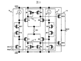
図2に本発明の別の実施例を示す。PMOSトランジスタM1、M2とNMOSトランジスタM5、M6はそれぞれ差動トランジスタ対を構成している。差動トランジスタ対のドレインは、それぞれNMOSトランジスタM3とM4で構成される能動負荷8とPMOSトランジスタM7、M8から成る能動負荷9に接続されている。トランジスタM9、M10、M11と電流源I1はレベル変換回路6を、トランジスタM12、M13、M14と電流源I2はレベル変換回路7を構成しており、M9とM12のゲートにそれぞれ信号Vin1とVin2が入力されている。NMOSトランジスタM15とPMOSトランジスタM16は出力段10を構成しており、M15,M16ともにソース接地で構成することにより高い駆動力と広い出力範囲の実現が可能である。また、ソース接地で出力段を構成しているため、負荷が容量性の場合には定常状態の場合にM15とM16をオフさせて電流が流れる経路を無くし、出力電圧を一定に保つことが可能である。これにより、定常状態では出力段で消費する電流を無くすことができる。本発明では差動トランジスタ対を直列に接続する構成を取っているため、差動対から電流電圧変換回路を用いて2つの出力を取り出すことにより、回路を追加することなく出力段をソース接地一般的なソースフォロワや電流源負荷のソース接地形式では定常的に電流を流す必要があるため、低電力化が可能となる。なお、本実施例では、レベル変換回路の出力電圧差をMOSトランジスタと定電流源で決定したが、電位差を発生させることができれば良いため、抵抗やバイポーラトランジスタを用いて構成することもできる。抵抗の抵抗値は任意に決定できるため、MOSトランジスタよりも詳細にレベル変換回路の出力電圧を設定できるという利点を持つ。バイアス電流源と入力トランジスタの位置関係も任意に組替えが可能である。また、出力段は、MOSトランジスタによるソース接地形式を用いたが、他の形式を用いることもできる。一例として、バイポーラトランジスタに置き換えることもできる。これにより、駆動力が増加するといった効果が得られる。電流電圧変換回路も、本実施例では能動負荷形式を用いたが、抵抗負荷など別の形式で構成してもよい。
FIG. 2 shows another embodiment of the present invention. The PMOS transistors M1 and M2 and the NMOS transistors M5 and M6 each constitute a differential transistor pair. The drains of the differential transistor pair are connected to an
図2の回路動作を、入力信号差の無い定常状態と差が生じた動作状態に分けて説明する。 The circuit operation of FIG. 2 will be described by dividing it into a steady state where there is no input signal difference and an operation state where a difference has occurred.
最初に入力信号差の無い場合、つまりVin1とVin2が等しい場合について説明する。入力信号Vin1とVin2はそれぞれレベル変換回路6のM9、レベル変換回路7のM12のゲートに入力されている。M9に入力されたVin1は、定電流源I1とM9によって決まるゲート―ソース電圧を加えた電位を差動トランジスタ対のM1へのゲートへ出力される。また、前記の電位にI1とダイオード接続されたM10、M11によって決まる電圧を加えたものがM5に出力される。回路形式は対称であり、M1とM2のゲート電位、及びM5とM6のゲート電位は等しい。このときに差動トランジスタ対に流れる定常電流は、レベル変換回路の2つの出力電位差と2つの差動トランジスタ対のトランジスタによって決まる。
First, a case where there is no input signal difference, that is, a case where Vin1 and Vin2 are equal will be described. The input signals Vin1 and Vin2 are input to the gates of M9 of the
この実施例においては、レベル変換回路のM1とM10,M5とM11のサイズ比は同じにすることにより、定常消費電流の制御が可能である。サイズ比を同じにすることで差動トランジスタ対のゲート―ソース間電圧が決まり、サイズ比とI1で決まる電流が定常電流として流れる。レベル変換部のトランジスタサイズと差動トランジスタ対のMOSサイズをm:nにしたとする。この時、入力電圧差が無い場合の定常電流としては、n/m*I1となる。回路は対称であるので、M2とM13,M6とM14のサイズ比に関しても同じとする。レベル変換回路の2つの出力電位差を生成する回路を、差動トランジスタ対と同様のNMOSとPMOSを直列接続した構成とすることにより、プロセスや温度の変動に対しても、レベル変換回路と差動トランジスタ対が変化を打ち消す方向に変化するようにし、定常電流の変化を小さくできる。 In this embodiment, the steady consumption current can be controlled by making the size ratios of M1 and M10 and M5 and M11 of the level conversion circuit the same. By making the size ratio the same, the gate-source voltage of the differential transistor pair is determined, and the current determined by the size ratio and I1 flows as a steady current. It is assumed that the transistor size of the level conversion unit and the MOS size of the differential transistor pair are m: n. At this time, the steady current when there is no input voltage difference is n / m * I1. Since the circuit is symmetrical, the same applies to the size ratio of M2 and M13, and M6 and M14. The level conversion circuit that generates the two output potential differences is configured by connecting NMOS and PMOS in the same way as the differential transistor pair in series, so that the level conversion circuit and the differential can be detected even with respect to process and temperature fluctuations. The transistor pair changes in a direction to cancel the change, and the change in the steady current can be reduced.
次に、入力信号に差が生じた動作状態について説明する。Vin1>Vin2の場合を考える。レベル変換回路は、入力信号に一定の電圧を加えた2つの電位を出力するため、M1のゲート電位はM2のゲート電位よりもVin1−Vin2だけ高く、M5のゲート電位もM6のゲート電位よりもVin1−Vin2だけ高くなる。入力信号に差が無い状態で、レベル変換回路の出力電位差が2つの差動トランジスタ対を形成するPMOSとNMOSのスレッショルド電圧の和に設定されているとする。M6のゲートとM1のゲートとの間にかかる電圧は、PMOSとNMOSのスレッショルド電圧の和よりもVin1−Vin2だけ小さくなる。よって、M1とM6はオフ状態となる。一方、M5のゲートとM2のゲートにかかる電圧は、PMOSとNMOSのスレッショルド電圧の和よりもVin1−Vin2だけ大きくなる。よって、M2とM5はオン状態となり、駆動電流が流れる。M5を流れた電流はM7とM8で構成される能動負荷によりミラーされ、M16をオフさせる。M2を流れた電流はM3とM4で構成される能動負荷によりミラーされ、M15をオンさせる。 Next, an operation state in which a difference occurs in the input signal will be described. Consider the case of Vin1> Vin2. Since the level conversion circuit outputs two potentials obtained by adding a constant voltage to the input signal, the gate potential of M1 is higher by Vin1-Vin2 than the gate potential of M2, and the gate potential of M5 is also higher than the gate potential of M6. It becomes higher by Vin1-Vin2. Assume that the output potential difference of the level conversion circuit is set to the sum of the threshold voltages of PMOS and NMOS forming two differential transistor pairs in a state where there is no difference in input signals. The voltage applied between the gate of M6 and the gate of M1 is smaller by Vin1-Vin2 than the sum of the threshold voltages of PMOS and NMOS. Therefore, M1 and M6 are turned off. On the other hand, the voltage applied to the gate of M5 and the gate of M2 is larger by Vin1-Vin2 than the sum of the threshold voltages of PMOS and NMOS. Therefore, M2 and M5 are turned on, and a drive current flows. The current flowing through M5 is mirrored by an active load consisting of M7 and M8, turning M16 off. The current flowing through M2 is mirrored by an active load consisting of M3 and M4, turning M15 on.
図3に本発明の別の実施例を示す。図3では駆動電流制御回路として抵抗R1を用いている。ここでは抵抗を用いることで、差動トランジスタ対に流れる電流によって電位降下が発生してゲート―ソース間電圧が減少し、消費電流の低減が可能である。レベル変換回路と差動トランジスタ対以外に駆動電流を制御できるパラメータが増え、定常電流と動作時の駆動力制御の調整が可能となる。R1を大きくした場合、差動トランジスタ対に流れる定常電流と動作時に流れる電流も減少する。なお、図2では駆動電流制御回路として抵抗を用いたが、トランジスタやその他の受動素子等を用いても構わない。 FIG. 3 shows another embodiment of the present invention. In FIG. 3, a resistor R1 is used as the drive current control circuit. Here, by using a resistor, a potential drop occurs due to the current flowing through the differential transistor pair, the gate-source voltage is reduced, and current consumption can be reduced. In addition to the level conversion circuit and the differential transistor pair, the number of parameters capable of controlling the driving current increases, and the steady current and the driving force control during operation can be adjusted. When R1 is increased, the steady current flowing through the differential transistor pair and the current flowing during operation are also reduced. In FIG. 2, a resistor is used as the drive current control circuit, but a transistor, other passive elements, or the like may be used.
図4に本発明の別の実施例を示す。差動対に用いているトランジスタのゲート―ソース間耐圧以上の入力電圧振幅差が入力された場合、トランジスタが破壊されてしまう。本発明は電源電圧が比較的高い場合の応用を想定しているため、ゲート―ソース間の耐圧がドレイン―ソース間耐圧よりも低いトランジスタを使用した場合には、耐圧を超える可能性がある。これを防ぐために、本実施例では耐圧保護のために耐圧保護素子の一例としてダイオードD1〜D8を追加している。耐圧保護用ダイオードの働きを説明するため、Vin1>Vin2の場合を考える。Vin1―Vin2がトランジスタM1,M2,M5,M6のゲート―ソース耐圧の2倍以上であるとする。このとき、M2とM5はオン状態、M1とM6はオフ状態である。M2とM5には電流が流れており、R1で電位降下が発生するため、適切なR1を選べばM2とM5への過電圧印加を防ぐことができる。一方、オフ状態のM1とM6のそれぞれのゲート間には、Vin1―Vin2がそのままM1とM6のゲート―ソース間に加わってしまう。このため、差動対のソース部分に耐圧保護ダイオードD1、D2、D3、D4を設置し、これを介してPMOSとNMOSの差動対を接続する。これにより、オフ状態のM1とM6のゲート―ソース間には電圧がかからず、Vin1―Vin2のほとんどがD1とD6に印加される。よって、M1とM6の破壊を防ぐことが可能になる。レベル変換回路の耐圧保護ダイオードD5,D6,D7,D8は、それぞれD1,D3,D2,D4に対応しており、温度が変動した場合などに差動対とレベル変換回路の特性が同様に変化するように対応させたもので、耐圧保護が目的では無い。よって、レベル変換回路部の耐圧保護ダイオードは省略可能である。また、耐圧保護素子はダイオードに限定されず、想定される過電圧に耐えられる耐圧を持つMOSトランジスタを耐圧保護素子として用いても構わない。 FIG. 4 shows another embodiment of the present invention. If an input voltage amplitude difference that exceeds the gate-source breakdown voltage of the transistor used in the differential pair is input, the transistor is destroyed. Since the present invention is supposed to be applied when the power supply voltage is relatively high, the use of a transistor having a gate-source breakdown voltage lower than the drain-source breakdown voltage may exceed the breakdown voltage. In order to prevent this, in this embodiment, diodes D1 to D8 are added as an example of a withstand voltage protection element for the withstand voltage protection. In order to explain the function of the withstand voltage protection diode, consider the case of Vin1> Vin2. It is assumed that Vin1-Vin2 is at least twice the gate-source breakdown voltage of the transistors M1, M2, M5, M6. At this time, M2 and M5 are on, and M1 and M6 are off. Since a current flows through M2 and M5 and a potential drop occurs at R1, application of an overvoltage to M2 and M5 can be prevented by selecting an appropriate R1. On the other hand, Vin1-Vin2 is directly added between the gate and source of M1 and M6 between the gates of M1 and M6 in the off state. For this reason, withstand voltage protection diodes D1, D2, D3, and D4 are installed in the source portion of the differential pair, and the PMOS-NMOS differential pair is connected thereto. As a result, no voltage is applied between the gate and source of M1 and M6 in the off state, and most of Vin1-Vin2 is applied to D1 and D6. Therefore, it becomes possible to prevent destruction of M1 and M6. The withstand voltage protection diodes D5, D6, D7, and D8 of the level conversion circuit correspond to D1, D3, D2, and D4, respectively, and the characteristics of the differential pair and the level conversion circuit change similarly when the temperature fluctuates. However, it is not intended to withstand pressure protection. Therefore, the withstand voltage protection diode in the level conversion circuit unit can be omitted. The withstand voltage protection element is not limited to a diode, and a MOS transistor having a withstand voltage that can withstand an assumed overvoltage may be used as the withstand voltage protection element.
図5に本発明の別の実施例を示す。演算増幅器が大きな負荷を駆動する場合、出力段のMOSトランジスタサイズは演算増幅器を構成する他のトランジスタよりも大きいため、入力電圧差の無い定常状態で出力段のMOSトランジスタのゲートーソース間にスレッショルド電圧Vth以上の電圧が入力されると、出力段にはトランジスタサイズに比例した電流が流れるため、消費電力が問題となる。この実施例では、電流電圧変換回路13を構成するNMOSトランジスタM17,M18を、出力段のNMOSトランジスタM15よりもVthが低いトランジスタで構成している。同様に、電流電圧変換回路14を構成するPMOSトランジスタM19,M20を、出力段のPMOSトランジスタM16よりもVthが低いトランジスタで構成している。入力電圧差の無い定常状態においては、出力段のPMOS、NMOSが消費する電流は、定常状態で電流電圧変換回路が出力する電圧、つまり、出力段のMOSトランジスタのゲート―ソース間電圧によって決まる。このため、電流電圧変換回路を構成するMOSトランジスタのVthを、出力段を構成するMOSトランジスタのVthよりも低くすることで、定常状態における電流電圧変換回路の出力電圧を、出力段のMOSトランジスタのVth以下に設定することができ、出力段のMOSトランジスタをオフした状態にすることが可能となる。なお、本実施例とは逆に出力段のVthを高くしても良い。
FIG. 5 shows another embodiment of the present invention. When the operational amplifier drives a large load, the MOS transistor size of the output stage is larger than the other transistors constituting the operational amplifier, so that the threshold voltage Vth between the gate and the source of the MOS transistor of the output stage in a steady state with no input voltage difference. When the above voltage is input, since a current proportional to the transistor size flows in the output stage, power consumption becomes a problem. In this embodiment, the NMOS transistors M17 and M18 constituting the current-
図6に本発明の別の実施例を示す。本実施例では、電流電圧変換回路8,9の出力に抵抗R2,R3を接続している。この抵抗を追加することにより、図5の実施例で説明したように、定常状態における電流電圧変換回路の出力電圧を、出力段のMOSトランジスタのVth以下にして、定常的な出力段での消費電流を低減している。R2とR3の抵抗値は、差動トランジスタ対に流れる電流に対して設計する必要がある。入力信号に信号差が生じた場合、差動トランジスタ対が駆動電流を流すが、抵抗R2,R3の抵抗値を駆動電流に対して小さくしすぎた場合、駆動電流が抵抗を流れてしまうことで出力段のトランジスタのゲート―ソース間電圧が低くなり、充分な駆動力を得られなくなる。また、本実施例では抵抗R1を駆動電流制限回路として用いているが、省略も可能である。
FIG. 6 shows another embodiment of the present invention. In this embodiment, resistors R2 and R3 are connected to the outputs of the current-
図7に本発明の別の実施例を示す。この回路は、Vinから入力された電圧を、抵抗R
4,R5の抵抗値をr4,r5とすると、(r4+r5)/r5倍し、本発明の演算増幅
器をボルテージホロワとして用いたバッファを介して出力している。この回路では、レベ
ル変換回路の低電力化を行うため、演算増幅器の前段の情報を用いてバイアス電流を制御
している。なお、演算増幅器前段の増幅回路の構成は、実施例の形式に限定されない。
FIG. 7 shows another embodiment of the present invention. This circuit converts a voltage input from Vin into a resistance R
If the resistance values of 4 and
回路動作を説明する。電源VDD2−VSS間の入力信号Vinは、定電流限I3によ
ってバイアスされた差動トランジスタ対M21,M22によって電流に変換される。変換
された電流は、M23とM25、M24とM26のカレントミラー対によって折り返され
る。M25で折り返された電流は、ゲート接地回路M27を介してVDD2よりも高い電
源VDDに接続されたカレントミラーM29,M30で再び折り返される。この電流は、
M26によって折り返された電流と比較され、ソースフォロワを構成するM31に入力さ
れる。抵抗R4、R5で分圧された電圧がVinと等しくなるように帰還がかかるため、
ソースフォロワの出力電位は、Vinの(r4+r5)/r5倍となる。この電圧は、ボ
ルテージホロワとして用いられる本発明の演算増幅器に入力され、バッファされて出力さ
れる。演算増幅器のレベル変換回路15,16は、前段のM29,M30で構成されるカ
レントミラーを用いて、バイアス電流を生成している。演算増幅器の入力Vin1,Vi
n2が増加したときには、M32,M33が流すバイアス電流がレベル変換回路出力の動
作速度が遅くなってしまうため、バイアス電流を多く流すことが求められる。一方。Vi
n1,Vin2が減少したときには、M9,M12がレベル変換回路の動作速度を決定す
るため、バイアス電流は小さくても良い。また、変化しないときには、レベル変換回路は
定常状態であるため電流は少なくても良い。このように、レベル変換回路のバイアス電流
が動作速度を決めているのは、演算増幅器の入力電圧が増加する場合である。前段のM2
9に流れる電流は、演算増幅器の入力電圧が増加する場合に多く、減少または入力が等し
い場合には減少するので、M29を用いてレベル変換回路の電流を生成することで、定常
状態での電力消費量を減少させることができる。
The circuit operation will be described. The input signal Vin between the power supplies VDD2 and VSS is converted into a current by the differential transistor pair M21 and M22 biased by the constant current limit I3. The converted current is folded back by the current mirror pair of M23 and M25 and M24 and M26. The current folded at M25 is folded again by the current mirrors M29 and M30 connected to the power supply VDD higher than VDD2 through the gate ground circuit M27. This current is
It is compared with the current turned back by M26 and input to M31 constituting the source follower. Since feedback is applied so that the voltage divided by the
The output potential of the source follower is (
When n2 increases, the bias current flowing through M32 and M33 slows down the operating speed of the level conversion circuit output, so that it is required to flow a large amount of bias current. on the other hand. Vi
When n1 and Vin2 decrease, the bias current may be small because M9 and M12 determine the operation speed of the level conversion circuit. When the level does not change, the level conversion circuit is in a steady state, so the current may be small. As described above, the bias current of the level conversion circuit determines the operation speed when the input voltage of the operational amplifier increases. Previous M2
9 is large when the input voltage of the operational amplifier increases, and decreases when the input voltage decreases or when the inputs are equal. Therefore, by generating the current of the level conversion circuit using M29, the power in the steady state Consumption can be reduced.
以上、本発明の各実施例によれば、レベル変換回路を用いることで入力信号差の検出回路と駆動能力制御回路を従来のような並列接続ではなく直列接続で実現したことにより、入力電圧が等しいときには演算増幅器で消費する電流を減らすことで消費電力を低減し、入力電圧に差が生じた時には演算増幅器で消費する電流を増加させ、スルーレートを改善することが可能となる。 As described above, according to the embodiments of the present invention, the input voltage difference detection circuit and the drive capability control circuit are realized by using a series connection instead of a conventional parallel connection by using a level conversion circuit. When equal, power consumption can be reduced by reducing the current consumed by the operational amplifier, and when a difference occurs in the input voltage, the current consumed by the operational amplifier can be increased to improve the slew rate.
尚、本発明の各実施例において、トランジスタはMOSを用いたが、バイポーラトランジスタで構成することも可能である。また、各実施例で用いた変形は、互いに組み合わせても有効である。レベル変換回路は上部電源側からバイアス電流を与えたが、下部電極側から与えてもよい。入力に関しても同様で、実施例では下部電源側から入力したが、上部電極側から入力しても良い。 In each embodiment of the present invention, a MOS transistor is used, but a bipolar transistor may be used. Further, the modifications used in each embodiment are effective even when combined with each other. In the level conversion circuit, the bias current is supplied from the upper power supply side, but may be supplied from the lower electrode side. The same applies to the input. In the embodiment, the input is performed from the lower power supply side, but the input may be performed from the upper electrode side.
1,2,6,7,11,12,15,16‥‥レベル変換回路、
3,4,8,9,13,14‥‥電流電圧変換回路、
5,10‥‥出力段、
M1,M2,M7,M8,M9,M10,M12,M13,M16,M19,M20,M21,M22,M29,M30‥‥PMOS、
M3,M4,M5,M6,M9,M10,M11,M14,M15,M17,M18,M23,M24,M25,M26,M27,M28,M31‥‥NMOS、
I1,I2,I3‥‥定電流源、
D1〜D8‥‥耐圧保護用ダイオード、
R1,R2,R3,R4,R5‥‥抵抗。
1, 2, 6, 7, 11, 12, 15, 16,... Level conversion circuit,
3, 4, 8, 9, 13, 14 ... current-voltage converter circuit,
5, 10 ... Output stage,
M1, M2, M7, M8, M9, M10, M12, M13, M16, M19, M20, M21, M22, M29, M30... PMOS
M3, M4, M5, M6, M9, M10, M11, M14, M15, M17, M18, M23, M24, M25, M26, M27, M28, M31 ... NMOS,
I1, I2, I3 ... Constant current source,
D1 to D8 ... withstand voltage protection diode,
R1, R2, R3, R4, R5 ... Resistance.
Claims (18)
前記レベル変換回路の差動出力が入力される差動増幅器と、
前記差動増幅器の出力に入力が接続される出力段と、
を備えて構成され、
前記レベル変換回路と前記差動増幅器との組合せが、前記差動入力信号のレベル差の検出と、該レベル差に応じた前記出力段に対する駆動能力の制御とを共通に行い、
前記レベル変換回路は、
前記差動入力信号の一方を入力とし、前記入力に所定の電圧を加えた第1の電位と前記第1の電位より高電位の第2の電位を出力する第1の出力対と、
前記差動入力信号の他方を入力とし、前記所定の電圧を加えた第3の電位と前記第3の電位より高電位の第4の電位を出力する第2の出力対とを有し、
前記差動増幅器は、
前記第2の電位及び前記第4の電位の出力を入力とし、それぞれの一端が第1の接続部で互いに接続される第1導電型トランジスタの差動対と、
前記第1の電位及び前記第3の電位の出力を入力とし、それぞれの一端が第2の接続部で互いに接続される第2導電型トランジスタの差動対と、
前記第1導電型トランジスタの差動対それぞれの他端が接続される第1の電流電圧変換回路と、
前記第2導電型トランジスタの差動対それぞれの他端が接続される第2の電流電圧変換回路と、
前記第1導電型トランジスタの差動対及び前記第2導電型トランジスタの差動対に流れる電流を低減する駆動電流制御回路と、を有し、
前記第1の電流電圧変換回路は第1の電源に接続され、
前記第2の電流電圧変換回路は前記第1の電源より低電位の第2の電源に接続され、
前記第1の接続部と前記第2の接続部とが、前記駆動電流制御回路を介して前記第1の電源と前記第2の電源に対して直列に接続されていることを特徴とする演算増幅器。 A level conversion circuit that converts the level of the differential input signal and outputs it differentially;
A differential amplifier to which the differential output of the level conversion circuit is input;
An output stage whose input is connected to the output of the differential amplifier;
Configured with
The combination of the level conversion circuit and the differential amplifier commonly performs detection of the level difference of the differential input signal and control of the driving capability for the output stage according to the level difference,
The level conversion circuit includes:
A first output pair that takes one of the differential input signals as an input, and outputs a first potential obtained by adding a predetermined voltage to the input and a second potential that is higher than the first potential;
Having the other of the differential input signals as an input, and a third potential to which the predetermined voltage is added and a second output pair for outputting a fourth potential higher than the third potential,
The differential amplifier is
A differential pair of first conductivity type transistors having inputs of the outputs of the second potential and the fourth potential and having one ends connected to each other at a first connection portion;
A differential pair of second-conductivity-type transistors, each having an output of the first potential and the third potential as inputs, and one ends of which are connected to each other at a second connection portion;
A first current-voltage conversion circuit to which the other end of each differential pair of the first conductivity type transistors is connected;
A second current-voltage conversion circuit to which the other end of each differential pair of the second conductivity type transistors is connected;
A drive current control circuit that reduces a current flowing through the differential pair of the first conductivity type transistor and the differential pair of the second conductivity type transistor;
The first current-voltage conversion circuit is connected to a first power source;
The second current-voltage conversion circuit is connected to a second power source having a lower potential than the first power source,
The calculation characterized in that the first connection part and the second connection part are connected in series to the first power supply and the second power supply via the drive current control circuit. amplifier.
前記第1導電型トランジスタの差動対は、前記第2の電位及び前記第4の電位の出力がゲートに入力され、ソース同士が前記第1の接続部で接続されるN型MOSトランジスタの差動対であり、
前記第2導電型トランジスタの差動対は、前記第1の電位及び前記第3の電位の出力がゲートに入力され、ソース同士が前記第2の接続部で接続されるP型MOSトランジスタの差動対であり、
前記N型MOSトランジスタの差動対それぞれのドレインが前記第1の電流電圧変換回路に接続され、
前記P型MOSトランジスタの差動対それぞれのドレインが前記第2の電流電圧変換回路に接続され、
前記駆動電流制御回路により、前記N型MOSトランジスタの差動対及び前記P型MOSトランジスタの差動対のゲート−ソース間電圧が減少することを特徴とする演算増幅器。 In claim 1,
The differential pair of the first conductivity type transistors is the difference between the N-type MOS transistors in which the outputs of the second potential and the fourth potential are input to the gate and the sources are connected to each other at the first connection portion. Moving pair,
The differential pair of the second conductivity type transistors is a difference between P-type MOS transistors in which the outputs of the first potential and the third potential are input to the gate and the sources are connected by the second connection portion. Moving pair,
The drains of the differential pairs of the N-type MOS transistors are connected to the first current-voltage conversion circuit,
The drains of the differential pairs of the P-type MOS transistors are connected to the second current-voltage conversion circuit,
An operational amplifier, wherein the drive current control circuit reduces a gate-source voltage of the differential pair of the N-type MOS transistor and the differential pair of the P-type MOS transistor.
前記駆動電流制御回路は抵抗素子を含んで構成されていることを特徴とする演算増幅器。 In claim 1,
An operational amplifier characterized in that the drive current control circuit includes a resistance element.
前記第1導電型トランジスタの差動対それぞれの一端に、前記第1の接続部に対して第1の耐圧保護素子が直列に接続され、
前記第2導電型トランジスタの差動対それぞれの一端に、前記第2の接続部に対して第2の耐圧保護素子が直列に接続されていることを特徴とする演算増幅器。 In claim 1,
A first withstand voltage protection element is connected in series to the first connection portion at one end of each differential pair of the first conductivity type transistors,
An operational amplifier, wherein a second withstand voltage protection element is connected in series to the second connection portion at one end of each differential pair of the second conductivity type transistor.
前記差動入力信号が無い定常状態にて前記第1の電流電圧変換回路の出力電圧を第1の所定電圧以下に抑えるための第1の抵抗素子が、前記第1の電流電圧変換回路の出力と前記第1の電源間に接続され、
前記差動入力信号が無い定常状態にて前記第2の電流電圧変換回路の出力電圧を第2の所定電圧以下に抑えるための第2の抵抗素子が、前記第2の電流電圧変換回路の出力と前記第2の電源間に接続され、
前記第1の所定電圧は、前記出力段を構成する第1のトランジスタに電流が流れない状態になるための閾値電圧であり、
前記第2の所定電圧は、前記出力段を構成する第2のトランジスタに電流が流れない状態になるための閾値電圧であることを特徴とする演算増幅器。 In claim 1,
The first resistance element for suppressing the output voltage of the first current-voltage conversion circuit below a first predetermined voltage in a steady state where there is no differential input signal is an output of the first current-voltage conversion circuit. And the first power supply,
The second resistance element for suppressing the output voltage of the second current-voltage conversion circuit below a second predetermined voltage in a steady state where there is no differential input signal is an output of the second current-voltage conversion circuit. And the second power source,
The first predetermined voltage is a threshold voltage for preventing a current from flowing through the first transistor constituting the output stage,
The operational amplifier according to claim 1, wherein the second predetermined voltage is a threshold voltage for preventing a current from flowing through the second transistor constituting the output stage.
前記レベル変換回路は、
前記第1の電源に接続される電流源とドレインが前記第2の電源に接続されるMOSトランジスタとの間に、ドレインとゲートを接続したP型MOSトランジスタ及びドレインとゲートを接続したN型MOSトランジスタとを含んで構成され、
前記出力段は、
前記第1の電流電圧変換回路の出力を入力とするソース接地P型MOSトランジスタと、前記第2の電流電圧変換回路の出力を入力とするソース接地N型MOSトランジスタを備えることを特徴とする演算増幅器。 In claim 1,
The level conversion circuit includes:
A P-type MOS transistor having a drain and a gate connected and a N-type MOS having a drain and a gate connected between a current source connected to the first power supply and a MOS transistor having a drain connected to the second power supply. Comprising a transistor,
The output stage is
An operation comprising: a source-grounded P-type MOS transistor that receives the output of the first current-voltage conversion circuit; and a source-grounded N-type MOS transistor that receives the output of the second current-voltage conversion circuit. amplifier.
前記第1の電流電圧変換回路は、前記第1導電型トランジスタの差動対それぞれのドレインにそれぞれのドレインが接続され、かつ、前記第1導電型トランジスタの差動対の一方のドレインに共通のゲートが接続され、かつ、前記第1導電型トランジスタの差動対の他方のドレインが出力となっている第1の能動負荷トランジスタ対を含んで構成され、
前記第2の電流電圧変換回路は、前記第2導電型トランジスタの差動対それぞれのドレインにそれぞれのドレインが接続され、かつ、前記第2導電型トランジスタの差動対の一方のドレインに共通のゲートが接続され、かつ、前記第2導電型トランジスタの差動対の他方のドレインが出力となっている第2の能動負荷トランジスタ対を含んで構成されることを特徴とする演算増幅器。 In claim 1,
In the first current-voltage conversion circuit, each drain is connected to each drain of the differential pair of the first conductivity type transistor, and is common to one drain of the differential pair of the first conductivity type transistor. A first active load transistor pair having a gate connected and the other drain of the differential pair of the first conductivity type transistors serving as an output;
The second current-voltage conversion circuit has a drain connected to each drain of the differential pair of the second conductivity type transistors, and is common to one drain of the differential pair of the second conductivity type transistors. An operational amplifier comprising a second active load transistor pair having a gate connected and the other drain of the differential pair of the second conductivity type transistors serving as an output.
前記第1および第2の耐圧保護素子はダイオードを含んで構成されていることを特徴とする演算増幅器。 In claim 4,
The operational amplifier according to claim 1, wherein the first and second withstand voltage protection elements include a diode.
前記第1および第2の耐圧保護素子はMOSトランジスタを含んで構成されていることを特徴とする演算増幅器。 In claim 4,
The operational amplifier according to claim 1, wherein the first and second breakdown voltage protection elements include MOS transistors.
前記入力信号の電位を変換して第3の電位と前記第3の電位より高電位の第4の電位を出力する第2のレベル変換回路と、A second level conversion circuit that converts the potential of the input signal to output a third potential and a fourth potential that is higher than the third potential;
前記第2の電位及び前記第4の電位の出力がゲートに入力され、ソース同士が前記第1の接続部で接続されるN型MOSトランジスタの差動対と、A differential pair of N-type MOS transistors in which outputs of the second potential and the fourth potential are input to a gate and sources are connected to each other at the first connection portion;
前記第1の電位及び前記第3の電位の出力がゲートに入力され、ソース同士が前記第2の接続部で接続されるP型MOSトランジスタの差動対と、A differential pair of P-type MOS transistors in which outputs of the first potential and the third potential are input to a gate and sources are connected to each other by the second connection portion;
前記N型MOSトランジスタの差動対それぞれのドレインが接続される第1の電流電圧変換回路と、A first current-voltage conversion circuit to which the drains of the differential pairs of the N-type MOS transistors are connected;
前記P型MOSトランジスタの差動対それぞれのドレインが接続される第2の電流電圧変換回路と、A second current-voltage conversion circuit to which the drains of the differential pairs of the P-type MOS transistors are connected;
前記第1及び第2の電流電圧変換回路の出力と電気的に接続され、前記第1及び第2の電流電圧変換回路により制御される出力段と、An output stage electrically connected to the outputs of the first and second current-voltage conversion circuits and controlled by the first and second current-voltage conversion circuits;
前記N型MOSトランジスタの差動対及び前記P型MOSトランジスタの差動対に流れる電流を低減する駆動電流制御回路と、を有し、A drive current control circuit for reducing a current flowing through the differential pair of the N-type MOS transistor and the differential pair of the P-type MOS transistor;
前記第1の電流電圧変換回路は第1の電源に接続され、The first current-voltage conversion circuit is connected to a first power source;
前記第2の電流電圧変換回路は前記第1の電源より低電位の第2の電源に接続され、The second current-voltage conversion circuit is connected to a second power source having a lower potential than the first power source,
前記第1の接続部と前記第2の接続部とが、前記駆動電流制御回路を介して前記第1の電源と前記第2の電源に対して直列に接続されていることを特徴とする演算増幅器。The calculation characterized in that the first connection part and the second connection part are connected in series to the first power supply and the second power supply via the drive current control circuit. amplifier.
前記駆動電流制御回路により、前記N型MOSトランジスタの差動対及び前記P型MOSトランジスタの差動対に流れる電流によって電位降下が発生して、前記ゲート−ソース間の電圧が減少することを特徴とする演算増幅器。The drive current control circuit causes a potential drop due to a current flowing through the differential pair of the N-type MOS transistor and the differential pair of the P-type MOS transistor, thereby reducing the voltage between the gate and the source. An operational amplifier.
前記駆動電流制御回路は抵抗素子を含んで構成されていることを特徴とする演算増幅器。An operational amplifier characterized in that the drive current control circuit includes a resistance element.
前記N型MOSトランジスタの差動対それぞれのソースに、前記第1の接続部に対して第1の耐圧保護素子が直列に接続され、A first withstand voltage protection element is connected in series to the first connection portion to the source of each differential pair of the N-type MOS transistor,
前記P型MOSトランジスタの差動対それぞれのソースに、前記第2の接続部に対して第2の耐圧保護素子が直列に接続されていることを特徴とする演算増幅器。An operational amplifier, wherein a source of each differential pair of the P-type MOS transistor is connected in series with a second withstand voltage protection element with respect to the second connection portion.
前記入力信号差が無い定常状態にて前記第1の電流電圧変換回路の出力電圧を第1の所定電圧以下に抑えるための第1の抵抗素子が、前記第1の電流電圧変換回路の出力と前記第1の電源間に接続され、A first resistance element for suppressing the output voltage of the first current-voltage conversion circuit to a first predetermined voltage or less in a steady state where there is no difference between the input signals is an output of the first current-voltage conversion circuit. Connected between the first power sources;
前記入力信号差が無い定常状態にて前記第2の電流電圧変換回路の出力電圧を第2の所定電圧以下に抑えるための第2の抵抗素子が、前記第2の電流電圧変換回路の出力と前記第2の電源間に接続され、A second resistance element for suppressing the output voltage of the second current-voltage conversion circuit to a second predetermined voltage or less in a steady state where there is no difference between the input signals is the output of the second current-voltage conversion circuit. Connected between the second power sources;
前記第1の所定電圧は、前記出力段を構成する第1のトランジスタに電流が流れない状態になるための閾値電圧であり、The first predetermined voltage is a threshold voltage for preventing a current from flowing through the first transistor constituting the output stage,
前記第2の所定電圧は、前記出力段を構成する第2のトランジスタに電流が流れない状態になるための閾値電圧であることを特徴とする演算増幅器。The operational amplifier according to claim 1, wherein the second predetermined voltage is a threshold voltage for preventing a current from flowing through the second transistor constituting the output stage.
前記第1及び第2のレベル変換回路それぞれは、Each of the first and second level conversion circuits includes:
前記第1の電源に接続される電流源とドレインが前記第2の電源に接続されるMOSトランジスタとの間に、ドレインとゲートを接続したP型MOSトランジスタ及びドレインとゲートを接続したN型MOSトランジスタとを含んで構成され、A P-type MOS transistor having a drain and a gate connected and a N-type MOS having a drain and a gate connected between a current source connected to the first power supply and a MOS transistor having a drain connected to the second power supply. Comprising a transistor,
前記出力段は、The output stage is
前記第1の電流電圧変換回路の出力を入力とするソース接地P型MOSトランジスタと、前記第2の電流電圧変換回路の出力を入力とするソース接地N型MOSトランジスタを備えることを特徴とする演算増幅器。An operation comprising: a source-grounded P-type MOS transistor that receives the output of the first current-voltage conversion circuit; and a source-grounded N-type MOS transistor that receives the output of the second current-voltage conversion circuit. amplifier.
前記第1の電流電圧変換回路は、前記N型MOSトランジスタの差動対それぞれのドレインにそれぞれのドレインが接続され、かつ、前記N型MOSトランジスタの差動対の一方のドレインに共通のゲートが接続され、かつ、前記N型MOSトランジスタの差動対の他方のドレインが出力となっている第1の能動負荷トランジスタ対を含んで構成され、In the first current-voltage conversion circuit, each drain is connected to a drain of each differential pair of the N-type MOS transistor, and a common gate is connected to one drain of the differential pair of the N-type MOS transistor. A first active load transistor pair connected and having the other drain of the differential pair of N-type MOS transistors as an output;
前記第2の電流電圧変換回路は、前記P型MOSトランジスタの差動対それぞれのドレインにそれぞれのドレインが接続され、かつ、前記P型MOSトランジスタの差動対の一方のドレインに共通のゲートが接続され、かつ、前記P型MOSトランジスタの差動対の他方のドレインが出力となっている第2の能動負荷トランジスタ対を含んで構成されることを特徴とする演算増幅器。In the second current-voltage conversion circuit, a drain is connected to each drain of the differential pair of the P-type MOS transistor, and a common gate is connected to one drain of the differential pair of the P-type MOS transistor. An operational amplifier comprising a second active load transistor pair connected and having the other drain of the differential pair of P-type MOS transistors as an output.
前記第1および第2の耐圧保護素子はダイオードを含んで構成されていることを特徴とする演算増幅器。The operational amplifier according to claim 1, wherein the first and second withstand voltage protection elements include a diode.
前記第1および第2の耐圧保護素子はMOSトランジスタを含んで構成されていることを特徴とする演算増幅器。The operational amplifier according to claim 1, wherein the first and second breakdown voltage protection elements include MOS transistors.
Priority Applications (2)
| Application Number | Priority Date | Filing Date | Title |
|---|---|---|---|
| JP2008009991A JP5094441B2 (en) | 2008-01-21 | 2008-01-21 | Operational amplifier |
| US12/354,309 US7982537B2 (en) | 2008-01-21 | 2009-01-15 | Operational amplifier |
Applications Claiming Priority (1)
| Application Number | Priority Date | Filing Date | Title |
|---|---|---|---|
| JP2008009991A JP5094441B2 (en) | 2008-01-21 | 2008-01-21 | Operational amplifier |
Publications (3)
| Publication Number | Publication Date |
|---|---|
| JP2009171479A JP2009171479A (en) | 2009-07-30 |
| JP2009171479A5 JP2009171479A5 (en) | 2011-01-20 |
| JP5094441B2 true JP5094441B2 (en) | 2012-12-12 |
Family
ID=40875993
Family Applications (1)
| Application Number | Title | Priority Date | Filing Date |
|---|---|---|---|
| JP2008009991A Expired - Fee Related JP5094441B2 (en) | 2008-01-21 | 2008-01-21 | Operational amplifier |
Country Status (2)
| Country | Link |
|---|---|
| US (1) | US7982537B2 (en) |
| JP (1) | JP5094441B2 (en) |
Families Citing this family (12)
| Publication number | Priority date | Publication date | Assignee | Title |
|---|---|---|---|---|
| US8692615B2 (en) * | 2012-03-20 | 2014-04-08 | Analog Devices, Inc. | Enhanced transconductance circuit |
| JP6124290B2 (en) * | 2013-03-15 | 2017-05-10 | 国立大学法人東京工業大学 | Operational amplifier |
| TWI561006B (en) * | 2013-05-24 | 2016-12-01 | Marvell Israel Misl Ltd | Systems and methods for data receipt from devices of disparate types |
| EP2879292B1 (en) * | 2013-11-28 | 2016-12-28 | ams AG | Amplifier arrangement |
| US9912229B2 (en) * | 2013-12-31 | 2018-03-06 | Texas Instruments Incorporated | Multiple output integrated power factor correction |
| WO2015190030A1 (en) * | 2014-06-12 | 2015-12-17 | 富士電機株式会社 | Operational amplifier and charge amplifier using same |
| EP3176945B1 (en) | 2015-12-04 | 2019-09-11 | ams AG | Switched capacitor integrator |
| JP2019012949A (en) * | 2017-06-30 | 2019-01-24 | ルネサスエレクトロニクス株式会社 | Semiconductor device |
| US10659033B2 (en) * | 2017-11-03 | 2020-05-19 | Texas Instruments Incorporated | High voltage gate driver current source |
| US11469727B2 (en) * | 2020-02-27 | 2022-10-11 | Texas Instruments Incorporated | Pre-driver stage with adjustable biasing |
| JP2021175124A (en) | 2020-04-28 | 2021-11-01 | キオクシア株式会社 | Semiconductor integrated circuit and semiconductor storage device |
| CN113067557B (en) * | 2021-04-01 | 2023-11-24 | 西安邮电大学 | High-speed full-differential comparator circuit with voltage conversion |
Family Cites Families (10)
| Publication number | Priority date | Publication date | Assignee | Title |
|---|---|---|---|---|
| US4180780A (en) * | 1978-10-02 | 1979-12-25 | Altec Corporation | Input decoupling circuit for transistor differential amplifier |
| US5343164A (en) * | 1993-03-25 | 1994-08-30 | John Fluke Mfg. Co., Inc. | Operational amplifier circuit with slew rate enhancement |
| JP3338771B2 (en) | 1997-09-04 | 2002-10-28 | 山形日本電気株式会社 | Operational amplifier |
| JP3376259B2 (en) | 1997-11-04 | 2003-02-10 | 日本電気株式会社 | Differential amplifier |
| JP3818793B2 (en) * | 1999-04-07 | 2006-09-06 | シャープ株式会社 | Sample hold circuit |
| JP2000349570A (en) | 1999-06-07 | 2000-12-15 | Toshiba Corp | Buffer circuit |
| US6262633B1 (en) * | 2000-04-27 | 2001-07-17 | Analog Devices, Inc. | High output current operational amplifier output stage |
| JP3847241B2 (en) * | 2002-10-01 | 2006-11-22 | Necエレクトロニクス株式会社 | Operational amplifier |
| JP2005303497A (en) * | 2004-04-08 | 2005-10-27 | Denso Corp | Differential amplifier circuit |
| JP3976097B2 (en) | 2004-11-30 | 2007-09-12 | 日本テキサス・インスツルメンツ株式会社 | amplifier |
-
2008
- 2008-01-21 JP JP2008009991A patent/JP5094441B2/en not_active Expired - Fee Related
-
2009
- 2009-01-15 US US12/354,309 patent/US7982537B2/en not_active Expired - Fee Related
Also Published As
| Publication number | Publication date |
|---|---|
| US7982537B2 (en) | 2011-07-19 |
| JP2009171479A (en) | 2009-07-30 |
| US20090184767A1 (en) | 2009-07-23 |
Similar Documents
| Publication | Publication Date | Title |
|---|---|---|
| JP5094441B2 (en) | Operational amplifier | |
| JP4616067B2 (en) | Constant voltage power circuit | |
| JP4834347B2 (en) | Constant current circuit | |
| TWI411904B (en) | Voltage regulator | |
| JP4805699B2 (en) | Semiconductor device | |
| JP4443301B2 (en) | Voltage regulator | |
| JP5657853B2 (en) | Constant current source circuit | |
| US7907003B2 (en) | Method for improving power-supply rejection | |
| JP4996203B2 (en) | Power supply voltage circuit | |
| JP2008015925A (en) | Reference voltage generation circuit | |
| WO2010026674A1 (en) | Reference voltage generating circuit | |
| JPH10509013A (en) | G <-m> -control circuit for input stage between CMOS feed lines by adjusting the sum of gate-source voltages constant | |
| JP2003298368A (en) | Amplifier circuit | |
| US7683687B2 (en) | Hysteresis characteristic input circuit including resistors capable of suppressing penetration current | |
| KR100885830B1 (en) | Limiter circuit | |
| KR100560260B1 (en) | Bias voltage generating circuit and differential amplifier | |
| JP2009094878A (en) | Differential amplification circuit | |
| JP4555131B2 (en) | Constant voltage power circuit | |
| JP2010141589A (en) | Differential amplifier circuit | |
| JP5369749B2 (en) | Constant voltage circuit | |
| JP2007180796A (en) | Differential amplifier circuit | |
| JP5849585B2 (en) | Overcurrent detection circuit | |
| JP2005333736A (en) | Overcurrent preventing circuit | |
| JP2002314399A (en) | Semiconductor integrated circuit | |
| JP5937302B2 (en) | Operational amplifier |
Legal Events
| Date | Code | Title | Description |
|---|---|---|---|
| A521 | Request for written amendment filed |
Free format text: JAPANESE INTERMEDIATE CODE: A523 Effective date: 20101126 |
|
| A621 | Written request for application examination |
Free format text: JAPANESE INTERMEDIATE CODE: A621 Effective date: 20101126 |
|
| A977 | Report on retrieval |
Free format text: JAPANESE INTERMEDIATE CODE: A971007 Effective date: 20111129 |
|
| A131 | Notification of reasons for refusal |
Free format text: JAPANESE INTERMEDIATE CODE: A131 Effective date: 20120104 |
|
| A521 | Request for written amendment filed |
Free format text: JAPANESE INTERMEDIATE CODE: A523 Effective date: 20120301 |
|
| TRDD | Decision of grant or rejection written | ||
| A01 | Written decision to grant a patent or to grant a registration (utility model) |
Free format text: JAPANESE INTERMEDIATE CODE: A01 Effective date: 20120821 |
|
| A01 | Written decision to grant a patent or to grant a registration (utility model) |
Free format text: JAPANESE INTERMEDIATE CODE: A01 |
|
| A61 | First payment of annual fees (during grant procedure) |
Free format text: JAPANESE INTERMEDIATE CODE: A61 Effective date: 20120918 |
|
| R151 | Written notification of patent or utility model registration |
Ref document number: 5094441 Country of ref document: JP Free format text: JAPANESE INTERMEDIATE CODE: R151 |
|
| FPAY | Renewal fee payment (event date is renewal date of database) |
Free format text: PAYMENT UNTIL: 20150928 Year of fee payment: 3 |
|
| S111 | Request for change of ownership or part of ownership |
Free format text: JAPANESE INTERMEDIATE CODE: R313113 |
|
| R350 | Written notification of registration of transfer |
Free format text: JAPANESE INTERMEDIATE CODE: R350 |
|
| R250 | Receipt of annual fees |
Free format text: JAPANESE INTERMEDIATE CODE: R250 |
|
| S533 | Written request for registration of change of name |
Free format text: JAPANESE INTERMEDIATE CODE: R313533 |
|
| R350 | Written notification of registration of transfer |
Free format text: JAPANESE INTERMEDIATE CODE: R350 |
|
| R250 | Receipt of annual fees |
Free format text: JAPANESE INTERMEDIATE CODE: R250 |
|
| R250 | Receipt of annual fees |
Free format text: JAPANESE INTERMEDIATE CODE: R250 |
|
| R250 | Receipt of annual fees |
Free format text: JAPANESE INTERMEDIATE CODE: R250 |
|
| LAPS | Cancellation because of no payment of annual fees |