JP5092012B2 - Spark plug for internal combustion engine - Google Patents
Spark plug for internal combustion engine Download PDFInfo
- Publication number
- JP5092012B2 JP5092012B2 JP2010515143A JP2010515143A JP5092012B2 JP 5092012 B2 JP5092012 B2 JP 5092012B2 JP 2010515143 A JP2010515143 A JP 2010515143A JP 2010515143 A JP2010515143 A JP 2010515143A JP 5092012 B2 JP5092012 B2 JP 5092012B2
- Authority
- JP
- Japan
- Prior art keywords
- tip
- noble metal
- metal tip
- relaxation layer
- ground electrode
- Prior art date
- Legal status (The legal status is an assumption and is not a legal conclusion. Google has not performed a legal analysis and makes no representation as to the accuracy of the status listed.)
- Active
Links
Images


Classifications
-
- H—ELECTRICITY
- H01—ELECTRIC ELEMENTS
- H01T—SPARK GAPS; OVERVOLTAGE ARRESTERS USING SPARK GAPS; SPARKING PLUGS; CORONA DEVICES; GENERATING IONS TO BE INTRODUCED INTO NON-ENCLOSED GASES
- H01T13/00—Sparking plugs
- H01T13/20—Sparking plugs characterised by features of the electrodes or insulation
- H01T13/39—Selection of materials for electrodes
-
- H—ELECTRICITY
- H01—ELECTRIC ELEMENTS
- H01T—SPARK GAPS; OVERVOLTAGE ARRESTERS USING SPARK GAPS; SPARKING PLUGS; CORONA DEVICES; GENERATING IONS TO BE INTRODUCED INTO NON-ENCLOSED GASES
- H01T13/00—Sparking plugs
- H01T13/20—Sparking plugs characterised by features of the electrodes or insulation
- H01T13/32—Sparking plugs characterised by features of the electrodes or insulation characterised by features of the earthed electrode
Description
本発明は、内燃機関に使用されるスパークプラグに関する。 The present invention relates to a spark plug used for an internal combustion engine.
自動車エンジン等の内燃機関に使用されるスパークプラグは、例えば軸線方向に延びる中心電極と、その外側に設けられた絶縁体と、当該絶縁体の外側に設けられた円筒状の主体金具と、基端部が前記主体金具の先端部に接合された接地電極とを備える。また、接地電極は、その先端部が前記中心電極の先端部と対向するように曲げ返して配置されるとともに、耐消耗性の向上を図るべく、当該先端部には貴金属チップが設けられる。 A spark plug used in an internal combustion engine such as an automobile engine includes, for example, a central electrode extending in the axial direction, an insulator provided outside the center electrode, a cylindrical metal shell provided outside the insulator, and a base. And a ground electrode joined to the tip of the metal shell. In addition, the ground electrode is bent back so that the tip portion thereof faces the tip portion of the center electrode, and a noble metal tip is provided at the tip portion in order to improve wear resistance.
ところで、接地電極の先端部に貴金属チップを設けるにあたっては、両者を抵抗溶接によって直接接合することが一般的である。ところが、この場合、接地電極を構成する金属材料と、貴金属チップを構成する金属材料との間における熱膨張の程度の差異によって、両者の間に大きな応力差が生じてしまうおそれがある。その結果、両者の接合部分にクラックが生じてしまい、ひいては接地電極から貴金属チップが剥離してしまうおそれがある。 By the way, when providing a noble metal tip at the tip of the ground electrode, it is common to directly join the two by resistance welding. However, in this case, a large stress difference may occur between the metal material constituting the ground electrode and the metal material constituting the noble metal tip due to the difference in thermal expansion. As a result, there is a possibility that a crack occurs at the joint portion between the two, and as a result, the noble metal tip may be peeled off from the ground electrode.
そこで、接地電極を構成する金属材料の線膨張係数と、貴金属チップを構成する金属材料の線膨張係数との間の線膨張係数を有する金属材料からなる緩和層チップを、接地電極と貴金属チップとの間に配設する手法が提案されている(例えば、特許文献1等参照)。当該技術によれば、接地電極及び緩和層チップ間、並びに、緩和層チップ及び貴金属チップ間における熱膨張の程度の差異を比較的小さなものとすることができ、ひいては接合部分におけるクラックの発生を抑制することができる。 Therefore, a relaxation layer chip made of a metal material having a linear expansion coefficient between the linear expansion coefficient of the metal material that constitutes the ground electrode and the linear expansion coefficient of the metal material that constitutes the noble metal tip, the ground electrode and the noble metal tip There has been proposed a method of arranging between the two (see, for example, Patent Document 1). According to this technology, the difference in the degree of thermal expansion between the ground electrode and the relaxation layer tip, and between the relaxation layer tip and the noble metal tip can be made relatively small, and thus the occurrence of cracks at the joint portion is suppressed. can do.
しかしながら、上記技術においては、貴金属チップと緩和層チップとが抵抗溶接によって接合されるため、緩和層チップに対する貴金属チップの接合強度を十分に確保することができない。加えて、接合部分において微小ながらもクラックが生じた場合には、当該クラックに対して酸素が侵入してしまい、ひいては接合部分において酸化スケールが進展してしまうおそれがある。従って、上記技術を採用した場合であっても、接地電極からの貴金属チップの剥離が依然として懸念される。 However, in the above technique, since the noble metal tip and the relaxation layer tip are joined by resistance welding, the joining strength of the noble metal tip to the relaxation layer tip cannot be sufficiently ensured. In addition, when a crack occurs even though it is minute in the joint portion, oxygen may enter the crack, and as a result, the oxide scale may develop in the joint portion. Therefore, even when the above technique is employed, there is still a concern about peeling of the noble metal tip from the ground electrode.
本発明は、上記事情を鑑みてなされたものであり、その目的は、貴金属チップ及び接地電極間に緩和層チップを備えてなる内燃機関用スパークプラグにおいて、貴金属チップを接地電極に対してより確実に接合するとともに、接合部分における酸化スケールの進展を抑制することで、接地電極からの貴金属チップの剥離をより確実に防止することができる内燃機関用スパークプラグを提供することにある。 The present invention has been made in view of the above circumstances, and an object of the present invention is to provide a spark plug for an internal combustion engine having a relaxation layer tip between a noble metal tip and a ground electrode, and the noble metal tip can be more reliably attached to the ground electrode. It is another object of the present invention to provide a spark plug for an internal combustion engine that can more reliably prevent exfoliation of a noble metal tip from a ground electrode by suppressing the progress of oxide scale at the joint portion.
以下、上記目的を解決するのに適した各構成につき、項分けして説明する。なお、必要に応じて対応する構成に特有の作用効果を付記する。 Hereinafter, each configuration suitable for solving the above-described object will be described in terms of items. In addition, the effect specific to the corresponding structure is added as needed.
構成1.本構成の内燃機関用スパークプラグは、軸線方向に延びる軸孔を有する絶縁体と、
前記軸孔に設けられた棒状の中心電極と、
前記絶縁体の外周に設けられた円筒状の主体金具と、
前記主体金具の先端部から延び、前記中心電極に向けて曲げられて配置された接地電極と、
前記接地電極の先端部に埋設された状態で抵抗溶接された板状の緩和層チップと、
前記緩和層チップの中心電極側の部位、及び、前記接地電極のうち前記緩和層チップの中心電極側の部位の外周側の部位に抵抗溶接される一端面、及び、前記中心電極の先端部との間で間隙を形成する他端面を有する貴金属チップとを備えた内燃機関用スパークプラグであって、
前記貴金属チップは、白金を主成分とする白金合金からなるとともに、
前記緩和層チップは、前記貴金属チップを形成する白金合金と、前記接地電極を形成する金属材料との間の線膨張係数を有する白金合金からなり、
前記緩和層チップのうち前記貴金属チップに接合される部位の面積が、前記貴金属チップの一端面の面積よりも小さく、かつ、
前記接地電極と、前記貴金属チップとの境界部の外周部分の全域に、少なくとも前記貴金属チップと前記接地電極とがレーザ溶接によって溶融されてなる溶融部が設けられていることを特徴とする。
A rod-shaped center electrode provided in the shaft hole;
A cylindrical metal shell provided on the outer periphery of the insulator;
A ground electrode that extends from the tip of the metal shell and is bent toward the center electrode; and
A plate-shaped relaxation layer tip resistance-welded in a state embedded in the tip of the ground electrode;
A portion of the relaxation layer tip on the center electrode side, and one end surface of the ground electrode that is resistance-welded to a portion on the outer peripheral side of the portion on the center electrode side of the relaxation layer tip, and a tip portion of the center electrode A spark plug for an internal combustion engine comprising a noble metal tip having a second end surface that forms a gap therebetween,
The noble metal tip is made of a platinum alloy mainly composed of platinum,
The relaxation layer tip is made of a platinum alloy having a linear expansion coefficient between a platinum alloy forming the noble metal tip and a metal material forming the ground electrode,
The area of the part to be joined to the noble metal tip of the relaxation layer tip is smaller than the area of one end surface of the noble metal tip, and
A melting portion is provided in which at least the noble metal tip and the ground electrode are melted by laser welding over the entire outer peripheral portion of the boundary portion between the ground electrode and the noble metal tip.
尚、中心電極の先端部に貴金属合金からなるチップを設けることとしてもよい。この場合、前記間隙は、中心電極側に設けられたチップと、接地電極に接合された貴金属チップとの間に形成されることとなる。 In addition, it is good also as providing the chip | tip which consists of noble metal alloys in the front-end | tip part of a center electrode. In this case, the gap is formed between the tip provided on the center electrode side and the noble metal tip joined to the ground electrode.
上記構成1によれば、接地電極及び貴金属チップ間には、貴金属チップを形成する白金合金と、接地電極を形成する金属材料との間の線膨張係数を有する白金合金からなる緩和層チップが設けられる。このため、接地電極及び緩和層チップ間、並びに、緩和層チップ及び貴金属チップ間における熱膨張の程度の差異を比較的小さなものとすることができ、緩和層チップと接地電極との接合部分や、緩和層チップと貴金属チップとの接合部分において大きな応力が発生してしまうことを抑制できる。その結果、接合部分におけるクラックの発生をより確実に抑制することができる。
According to the
また、本構成1によれば、貴金属チップは、接地電極に埋設された緩和層チップのうち中心電極側の部位と、接地電極のうち前記緩和層チップの中心電極側の部位の外周側に位置する部位との双方に対して抵抗溶接されている。加えて、接地電極と、貴金属チップとの境界部分の外周部分全域に、レーザ溶接によって溶融部が形成されている。すなわち、貴金属チップは、抵抗溶接、及び、レーザ溶接の双方によって接地電極及び緩和層チップに接合されるため、接地電極等に対する貴金属チップの接合をより強固なものとすることができる。併せて、貴金属チップを構成する白金合金と接地電極を構成する金属材料とが溶融してなる溶融部は、貴金属チップと接地電極との間において、上述した緩和層チップと同様の働きをし、両者の間における大きな応力の発生を抑制することができる。さらに、前記溶融部は、貴金属チップ及び緩和層チップ間の接合部分(境界部分)を覆うこととなる。そのため、仮に当該接合部分にクラックが生じてしまったとしても、溶融部の存在によって、クラックに対する酸素の侵入を効果的に防止することができ、酸化スケールの進展をより確実に防止することができる。
According to the
以上のように、本構成1によれば、上述の各作用効果が相乗的に作用することにより、接地電極からの貴金属チップの剥離を効果的に防止することができる。
As described above, according to the
尚、緩和層チップとしては、貴金属チップに抵抗溶接される部位の面積が、貴金属チップの一端面の面積よりも小さなものが用いられる。すなわち、比較的小型の緩和層チップを用いることで、緩和層チップを設けるにあたってのコストの増大を抑制することができる。 In addition, as a relaxation layer chip | tip, the area | region of the site | part resistance-welded to a noble metal tip is smaller than the area of the one end surface of a noble metal tip. That is, by using a relatively small relaxation layer chip, it is possible to suppress an increase in cost in providing the relaxation layer chip.
ところで、上記特許文献1に示すような、貴金属チップと接地電極とが接触しない構成において、貴金属チップと緩和層チップとの境界部分の外周にレーザ溶接による溶融部を設けることで、両者の接合部分に対する酸素の侵入を防止し、酸化スケールの進展を防止する手法も考えられる。ところが、貴金属チップや緩和層チップは、比較的溶融しにくい合金(貴金属合金)によって形成されるのが一般的であるため、両者を溶融するにあたっては比較的大きな溶融エネルギーが必要となる。ところが、レーザビームの溶融エネルギーを増大させた場合には、貴金属チップや緩和層チップに熱エネルギーが蓄積されてしまい、ひいては同一の溶融エネルギーでレーザビームを照射したとしても、溶融部のうち最初に形成される部分と、溶融部のうち最後に形成される部分とでは、その溶融の程度に相違が生じてしまうおそれがある。従って、溶融部をムラなく形成するためには、レーザビームの照射エネルギーや照射角度を細かく調整することが必要となるが、その調整は非常に難しい。
By the way, in the configuration in which the noble metal tip and the ground electrode are not in contact with each other as shown in
この点、本構成1によれば、緩和層チップとして、貴金属チップに抵抗溶接される部位の面積が、貴金属チップの一端面の面積も小さくなるものが用いられる。そのため、緩和層チップとして、貴金属チップに抵抗溶接される部位の面積が、貴金属チップの一端面の面積と等しいものを用いた場合と比較して、溶融部は、接地電極を構成する金属材料が比較的多く含有して形成されることとなる。ここで、接地電極を構成する金属材料については、一般的にニッケル合金等が用いられ、緩和層チップよりも溶融に必要なエネルギーが少なくて済む。従って、溶融部を形成するために必要な溶融エネルギーの低減を図ることができ、レーザビームの照射エネルギーや照射角度について細かい調整を特に要することなく、溶融部を比較的容易に、かつ、ムラなく形成することができる。すなわち、緩和層チップとして比較的小さなものを用いることは、コストの増大抑制を実現するという点だけでなく、溶融部をムラなく形成し、酸化スケールの進展を効果的に防止するという点においても有意である。
In this regard, according to the
構成2.本構成の内燃機関用スパークプラグは、上記構成1において、前記緩和層チップのうち前記貴金属チップに抵抗溶接される部位の面積は、前記貴金属チップの一端面の面積の45%以上75%以下であることを特徴とする。
Configuration 2. The spark plug for an internal combustion engine according to this configuration is the
上記構成2によれば、緩和層チップのうち貴金属チップに抵抗溶接される部位の面積が、貴金属チップの一端面の面積の45%以上とされている。このため、貴金属チップと緩和層チップとの接合部分等において大きな応力が発生してしまうことをより確実に抑制でき、ひいては接合部分におけるクラックの発生や酸化スケールの進展を一層確実に防止することができる。 According to Configuration 2, the area of the relaxation layer tip that is resistance-welded to the noble metal tip is 45% or more of the area of one end face of the noble metal tip. For this reason, it can suppress more reliably that big stress will generate | occur | produce in the junction part etc. of a noble metal chip | tip and a relaxation layer chip | tip, and it can prevent generation | occurrence | production of the crack in a junction part, and an oxide scale further reliably. it can.
また、緩和層チップのうち貴金属チップに抵抗溶接される部位の面積が、貴金属チップの一端面の面積の75%以下とされているため、コストの増大抑制をより一層図ることができるとともに、均一な溶融部をより確実に実現することができる。 Further, since the area of the portion of the relaxation layer tip that is resistance-welded to the noble metal tip is 75% or less of the area of the one end face of the noble metal tip, the increase in cost can be further suppressed and uniform. It is possible to realize a more reliable melting part more reliably.
構成3.本構成の内燃機関用スパークプラグは、上記構成1又は2において、前記緩和層チップのうち前記貴金属チップに抵抗溶接される部位の面積は、前記貴金属チップの一端面の面積の60%以上75%以下であることを特徴とする。
上記構成3によれば、緩和層チップのうち貴金属チップに抵抗溶接される部位の面積が、貴金属チップの一端面の面積の60%以上75%以下とされている。このため、貴金属チップと緩和層チップとの接合部分等において大きな応力が発生してしまうことをより効果的に抑制できる。
According to the
構成4.本構成の内燃機関用スパークプラグは、上記構成1乃至3のいずれかにおいて、前記緩和層チップ、及び、前記貴金属チップは、円板状をなすとともに、
前記緩和層チップのうち前記貴金属チップに抵抗溶接される部位の外径は、前記貴金属チップの一端面の外径の68%以上86%以下であることを特徴とする。Configuration 4. The spark plug for the internal combustion engine of the present configuration has any one of the
An outer diameter of a portion of the relaxation layer tip that is resistance-welded to the noble metal tip is 68% to 86% of an outer diameter of one end face of the noble metal tip.
上記構成4によれば、基本的には上記構成2と同様の作用効果が奏されることとなる。 According to the said structure 4, the effect similar to the said structure 2 will be show | played fundamentally.
構成5.本構成の内燃機関用スパークプラグは、上記構成1乃至4のいずれかにおいて、前記緩和層チップ、及び、前記貴金属チップは、円板状をなすとともに、
前記緩和層チップのうち前記貴金属チップに抵抗溶接される部位の外径は、前記貴金属チップの一端面の外径の77%以上86%以下であることを特徴とする。
An outer diameter of a portion of the relaxation layer tip that is resistance-welded to the noble metal tip is not less than 77% and not more than 86% of an outer diameter of one end face of the noble metal tip.
上記構成5によれば、基本的には上記構成3と同様の作用効果が奏されることとなる。
According to the said
構成6.本構成の内燃機関用スパークプラグは、上記構成1乃至5のいずれかにおいて、前記貴金属チップの一端面の面積は、1.7mm2以上であることを特徴とする。
貴金属チップは、緩和層チップや接地電極に接合される部位の面積が大きいほど、貴金属チップ及び緩和層チップの接合部分等において発生する応力が大きくなる。そのため、例えば、耐消耗性の向上を図るべく、比較的大きな貴金属チップを用いた場合には、前記接合部分におけるクラックの発生や酸化スケールの進展、ひいては貴金属チップの剥離が一層懸念される。 In the noble metal tip, as the area of the part to be joined to the relaxing layer tip or the ground electrode is larger, the stress generated at the joining part of the noble metal tip and the relaxing layer tip is increased. Therefore, for example, when a relatively large noble metal tip is used in order to improve wear resistance, there is a further concern about the occurrence of cracks in the joint portion, the progress of oxide scale, and the separation of the noble metal tip.
ここで、上記構成6の貴金属チップは、接地電極や緩和層チップに接合される一端面の面積が1.7mm2以上と比較的大きな面積を有するものであり、貴金属チップの剥離が懸念されるところであるが、上記構成1等を採用することで、貴金属チップの剥離を効果的に防止することができる。すなわち、貴金属チップの一端面(接合面)の面積が比較的大きな場合において、上記構成1等を採用することがより有意であるといえる。Here, the noble metal tip having the
構成7.本構成の内燃機関用スパークプラグは、上記構成1乃至6のいずれかにおいて、前記貴金属チップは、その一端部が前記接地電極に対して埋め込まれた状態で溶融接合されるとともに、
前記接地電極に対する前記貴金属チップの埋め込み量を、埋め込み前の前記貴金属チップの高さの25%以下としたことを特徴とする。
The amount of the precious metal tip embedded in the ground electrode is 25% or less of the height of the precious metal tip before embedding.
上記構成7によれば、貴金属チップは接地電極に対して一端部が埋め込まれた状態で接合されているが、接地電極に対する貴金属チップの埋め込み量は、埋め込み前の貴金属チップの高さの25%以下とされている。ここで、貴金属チップを接地電極に対して過度に埋め込んだ場合には、接地電極の変形(盛上がり)が生じてしまい、当該変形部分と中心電極との間の不正常な火花放電等の不具合が発生し得るが、本構成7によれば、このような不具合の発生をより確実に抑制することができる。
According to the
構成8.本構成の内燃機関用スパークプラグは、上記構成1乃至7のいずれかにおいて、前記溶融部中において、白金の含有量を1とし、その他の金属材料の含有量を3〜10としたことを特徴とする。
上記構成8によれば、溶融部を構成する金属材料について、白金の含有量を1としたとき、その他の金属材料の含有量が3〜10とされている。すなわち、溶融部を形成するにあたっては、主として接地電極を構成する金属材料が溶融されるため、溶融部を形成するために必要な溶融エネルギーを一層低減させることができる。従って、レーザビームの照射エネルギーや照射角度について細かい調整を要することなく、溶融部を一層容易に、ムラなく形成することができる。
According to the said
また、上記構成8によれば、溶融部及び接地電極間、並びに、溶融部及び貴金属チップ間における熱膨張の程度の差異を双方ともに比較的小さなものとすることができ、溶融部における割れ(クラック)の発生をより確実に抑制することができる。その結果、貴金属チップ及び緩和層チップの接合部分等に対する酸素の侵入をより一層確実に防止することができ、ひいては酸化スケールの進展を一層効果的に防止することができる。
Further, according to the above-described
尚、溶融部において、白金の含有量を1としたとき、その他の金属材料の含有量を3未満とした場合には、溶融部を形成するための溶融エネルギーの増大を招いてしまい、溶融部を均一に形成することが難しくなってしまったり、また、溶融部と接地電極との間における熱膨張の程度に比較的大きな差が生じてしまい、溶融部の割れが生じやすくなってしまうおそれがある。一方で、溶融部においてその他の金属材料の含有量が10を超えるようにした場合には、貴金属チップが接地電極に対して十分に接合されず、ひいては貴金属チップの耐剥離性の向上効果が十分に発揮されなかったり、また、溶融部に割れが生じやすくなってしまうおそれがある。 In the melting part, when the platinum content is 1 and the content of the other metal material is less than 3, the melting energy for forming the melting part is increased, and the melting part It may be difficult to form a uniform layer, or a relatively large difference may occur in the degree of thermal expansion between the melted portion and the ground electrode, which may cause cracks in the melted portion. is there. On the other hand, when the content of the other metal material exceeds 10 in the molten part, the noble metal tip is not sufficiently bonded to the ground electrode, and thus the effect of improving the peel resistance of the noble metal tip is sufficient. May not be exhibited, and cracks may easily occur in the melted portion.
構成9.本構成の内燃機関用スパークプラグは、上記構成8において、前記溶融部のうち最も径方向外側に位置する部位の外径をA(mm)とし、
前記溶融部のうち最も径方向内側に位置する部位の内径をB(mm)としたとき、
0.45≦B/A≦0.68
を満たすことを特徴とする。
When the inner diameter of the portion located on the radially inner side of the melted portion is B (mm),
0.45 ≦ B / A ≦ 0.68
It is characterized by satisfying.
上記構成9によれば、溶融部は、白金とその他の金属材料とがよりバランスよく含有されて構成されることとなる。その結果、溶融部における割れの発生をより一層確実に防止することができ、酸化スケールの進展をより一層効果的に防止することができる。
According to the said
尚、B/Aを0.45未満とした場合(すなわち、溶融部を比較的深く形成した場合)には、溶融部中において、白金以外の金属材料の含有量が相対的に増加し得る。従って、溶融部と貴金属チップとの間における熱膨張の程度の差異が若干増大してしまうおそれがある。一方で、B/Aが0.68を超える場合(すなわち、溶融部を比較的浅く形成した場合)には、溶融部中において、白金の含有量が相対的に増加し、その結果、溶融部と接地電極との間における熱膨張の程度の差異が若干増大してしまうおそれがある。但し、溶融部と、貴金属チップ或いは接地電極との間における熱膨張の程度の差異が若干増大したとしても、上記構成8を満たすこと(つまり、溶融部中において、白金の含有量を1としたとき、その他の金属材料の含有量を3〜10とすること)で、溶融部の割れは十分に抑制可能である。
When B / A is less than 0.45 (that is, when the melted part is formed relatively deep), the content of metal materials other than platinum can be relatively increased in the melted part. Therefore, the difference in the degree of thermal expansion between the melted part and the noble metal tip may be slightly increased. On the other hand, when B / A exceeds 0.68 (that is, when the melted part is formed relatively shallow), the platinum content is relatively increased in the melted part. The difference in the degree of thermal expansion between the ground electrode and the ground electrode may slightly increase. However, even if the difference in the degree of thermal expansion between the molten part and the noble metal tip or the ground electrode is slightly increased, the
構成10.本構成の内燃機関用スパークプラグは、上記構成1乃至9のいずれかにおいて、前記溶融部は、レーザビームを照射することで形成された複数の溶融領域が連なることで形成されており、
前記各溶融領域の表面は、自身に隣接する溶融領域の20%以上60%以下の領域で重なり合って形成されることを特徴とする。
The surface of each melting region is formed so as to overlap in a region of 20% or more and 60% or less of a melting region adjacent to itself.
上記構成10によれば、溶融部は複数の溶融領域が連続することで形成されており、各溶融領域の表面は、自身に隣接する溶融領域の20%以上の領域と重なり合うようにして設けられている。従って、溶融部がより強固に形成されることとなり、接合部分における酸化スケールの進展等をより一層確実に抑制することができる。
According to the
一方で、各溶融領域の表面において、隣接する溶融領域と重なり合う領域は、当該隣接する溶融領域の60%以下とされる(すなわち、各溶融領域が過度に重なり過ぎていない)ため、溶融部の形成を比較的短時間に行うことができ、生産効率の向上を図ることができる。 On the other hand, on the surface of each melting region, the region overlapping with the adjacent melting region is 60% or less of the adjacent melting region (that is, each melting region is not excessively overlapped). The formation can be performed in a relatively short time, and the production efficiency can be improved.
以下に、一実施形態について図面を参照して説明する。図1は、主としてガスエンジン等、使用条件の厳しいエンジンに用いられる内燃機関用スパークプラグ(以下、「スパークプラグ」と称す)1を示す一部破断正面図である。尚、図1では、スパークプラグ1の軸線CL1方向を図面における上下方向とし、下側をスパークプラグ1の先端側、上側を後端側として説明する。
Hereinafter, an embodiment will be described with reference to the drawings. FIG. 1 is a partially broken front view showing a spark plug for an internal combustion engine (hereinafter referred to as “spark plug”) 1 mainly used in an engine having severe use conditions such as a gas engine. In FIG. 1, the direction of the axis CL <b> 1 of the
スパークプラグ1は、筒状をなす絶縁体としての絶縁碍子2、これを保持する筒状の主体金具3などから構成されるものである。
The
絶縁碍子2は、周知のようにアルミナ等を焼成して形成されており、その外形部において、後端側に形成された後端側胴部10と、当該後端側胴部10よりも先端側において径方向外向きに突出形成された大径部11と、当該大径部11よりも先端側においてこれよりも細径に形成された中胴部12とを備えている。また、前記絶縁碍子2は、前記中胴部12よりも先端側において、先端側に向けて先細り形状をなす脚長部13を有しており、絶縁碍子2のうち、大径部11、中胴部12、及び、大部分の脚長部13は、主体金具3の内部に収容されている。そして、脚長部13と中胴部12との連接部にはテーパ状の段部14が形成されており、当該段部14にて絶縁碍子2が主体金具3に係止されている。
As is well known, the insulator 2 is formed by firing alumina or the like, and in its outer portion, a rear end
さらに、絶縁碍子2には、軸線CL1に沿って軸孔4が貫通形成されており、当該軸孔4の先端側には中心電極5が挿入、固定されている。当該中心電極5は、全体として棒状(円柱状)をなし、その先端面が平坦に形成されるとともに、絶縁碍子2の先端から突出している。また、中心電極5は、銅又は銅合金からなる内層5Aと、ニッケル(Ni)を主成分とするNi合金からなる外層5Bとを備えている。さらに、前記中心電極5の先端部には、貴金属合金(例えば、白金合金やイリジウム合金等)よりなる円柱状の貴金属チップ31が接合されている。
Further, the insulator 2 is formed with a shaft hole 4 penetrating along the axis CL1, and a
また、軸孔4の後端側には、絶縁碍子2の後端から突出した状態で端子電極6が挿入、固定されている。
A
さらに、軸孔4の中心電極5と端子電極6との間には、円柱状の抵抗体7が配設されている。当該抵抗体7の両端部は、導電性のガラスシール層8,9を介して、中心電極5と端子電極6とにそれぞれ電気的に接続されている。
Further, a
加えて、前記主体金具3は、低炭素鋼等の金属により形成されており、その外周面にはスパークプラグ1をエンジンヘッドに取付けるためのねじ部(雄ねじ部)15が形成されている。また、ねじ部15の後端側の外周面には座部16が形成され、ねじ部15後端のねじ首17にはリング状のガスケット18が嵌め込まれている。さらに、主体金具3の後端側には、主体金具3をエンジンヘッドに取付ける際にレンチ等の工具を係合させるための断面六角形状の工具係合部19が設けられるとともに、後端部において絶縁碍子2を保持するための加締め部20が設けられている。
In addition, the
また、主体金具3の内周面には、絶縁碍子2を係止するためのテーパ状の段部21が設けられている。そして、絶縁碍子2は、主体金具3の後端側から先端側に向かって挿入され、自身の段部14が主体金具3の段部21に係止された状態で、主体金具3の後端側の開口部を径方向内側に加締めること、つまり上記加締め部20を形成することによって固定される。尚、絶縁碍子2及び主体金具3双方の段部14,21間には、円環状の板パッキン22が介在されている。これにより、燃焼室内の気密性を保持し、燃焼室内に晒される絶縁碍子2の脚長部13と主体金具3の内周面との間隙に入り込む燃料空気が外部に漏れないようになっている。
A
さらに、加締めによる密閉をより完全なものとするため、主体金具3の後端側においては、主体金具3と絶縁碍子2との間に環状のリング部材23,24が介在され、リング部材23,24間にはタルク(滑石)25の粉末が充填されている。すなわち、主体金具3は、板パッキン22、リング部材23,24及びタルク25を介して絶縁碍子2を保持している。
Further, in order to make the sealing by caulking more complete,
加えて、主体金具3の先端部26に対して、Ni合金で構成された接地電極27が接合されている。当該接地電極27は、自身の略中間部分が曲げ返されており、接地電極27の先端部のうち中心電極5側の側面27Fが中心電極5(貴金属チップ31)の先端面と対向している。
In addition, a ground electrode 27 made of an Ni alloy is joined to the
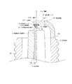
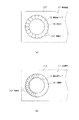
また、図2に示すように、前記接地電極27の側面27Fには、円板状をなす緩和層チップ32が埋設状態で抵抗溶接されている。さらに、緩和層チップ32のうち中心電極5側に位置する部位(以下、便宜上「上面部32F」という)、及び、接地電極27のうち前記上面部32Fの外周側に位置する部位に対して円板状をなす貴金属チップ33が抵抗溶接等によって接合されている。また、前記貴金属チップ31の先端面と貴金属チップ33の他端面33Aとの間には、前記軸線CL1にほぼ沿って火花放電が行われる火花放電間隙34が形成されている。
In addition, as shown in FIG. 2, the side surface 27 </ b> F of the ground electrode 27 is resistance-welded in a buried state with a disk-shaped relaxation layer tip 32. Further, a portion of the relaxation layer chip 32 positioned on the
尚、本実施形態において、前記貴金属チップ33は、白金(Pt)を主成分とするPt合金(例えば、Pt−Ir合金、Pt−Rh合金、Pt−Ni合金、Pt−Ir−Rh合金等)により形成されている。また、前記緩和層チップ32は、貴金属チップ33を形成するPt合金、及び、接地電極27を形成するNi合金の間の線膨張係数を有するPtを主成分とするPt合金(例えば、Pt−Ni合金等)により形成されている。ここで、前記貴金属チップ33は、消耗体積を増大させるべく、比較的厚肉(例えば、0.4mm以上)に形成されている一方で、前記緩和層チップ32は、前記貴金属チップ33と比較して薄肉(例えば、0.2mm〜0.35mm)に形成されている。これにより、緩和層チップ32が埋設される接地電極27については、埋設に伴う変形を極力抑制できるようになっており、ひいては接地電極27や緩和層チップ32に対して貴金属チップ33をより確実に抵抗溶接できるようになっている。 In the present embodiment, the noble metal tip 33 is a Pt alloy mainly composed of platinum (Pt) (for example, a Pt—Ir alloy, a Pt—Rh alloy, a Pt—Ni alloy, a Pt—Ir—Rh alloy, etc.). It is formed by. Further, the relaxation layer chip 32 is made of a Pt alloy mainly composed of Pt having a linear expansion coefficient between the Pt alloy forming the noble metal chip 33 and the Ni alloy forming the ground electrode 27 (for example, Pt—Ni). Alloy). Here, the noble metal tip 33 is formed to be relatively thick (for example, 0.4 mm or more) in order to increase the consumption volume, while the relaxation layer tip 32 is compared with the noble metal tip 33. And thin (for example, 0.2 mm to 0.35 mm). As a result, the ground electrode 27 in which the relaxation layer chip 32 is embedded can be restrained from being deformed as much as possible. As a result, the noble metal tip 33 is more reliably attached to the ground electrode 27 and the relaxation layer chip 32. Resistance welding is now possible.
さらに、緩和層チップ32の中心軸に沿った緩和層チップ32の断面積は、貴金属チップ33の中心軸に沿った貴金属チップ33の断面積よりも小さなものとされており、ひいては緩和層チップ32のうち貴金属チップ33に接合される上面部32Fの面積は、貴金属チップ33の一端面33Bの面積よりも小さくされている。より詳しくは、緩和層チップ32の上面部32Fの面積は、貴金属チップ33の一端面33Bの面積の45%以上75%以下(例えば、60%)とされている(換言すれば、緩和層チップ32の上面部32Fの外径は、貴金属チップ33の一端面33Bの外径の68%以上86%以下とされている)。尚、本実施形態において、貴金属チップ33は、消耗体積の一層の増大を図るべく、比較的大径化(φ1.5mm以上)されており、比較的大きな断面積(例えば、1.7mm2以上)を有している。Furthermore, the cross-sectional area of the relaxation layer chip 32 along the central axis of the relaxation layer chip 32 is smaller than the cross-sectional area of the noble metal chip 33 along the central axis of the noble metal chip 33. Of these, the area of the upper surface portion 32F joined to the noble metal tip 33 is smaller than the area of the one end face 33B of the noble metal tip 33. More specifically, the area of the upper surface portion 32F of the relaxation layer chip 32 is 45% or more and 75% or less (for example, 60%) of the area of the one end surface 33B of the noble metal chip 33 (in other words, the relaxation layer chip). The outer diameter of the upper surface part 32F of 32 is 68% or more and 86% or less of the outer diameter of the one end face 33B of the noble metal tip 33). In this embodiment, the noble metal tip 33 has a relatively large diameter (φ1.5 mm or more) in order to further increase the consumption volume, and has a relatively large cross-sectional area (for example, 1.7 mm 2 or more). )have.
さらに、前記接地電極27と、貴金属チップ33の一端面33Bとの境界部の全周には、緩和層チップ32を構成するPt合金、貴金属チップ33を構成するPt合金、及び、接地電極27を構成するNi合金とがレーザ溶接によって溶融されてなる環状の溶融部36が設けられている。当該溶融部36は、図3(a)に示すように、レーザビームを間欠的に照射することで形成された複数の溶融領域としての溶融点36Pが連なることで形成されている。尚、各溶融点36Pの表面は、自身に隣接する溶融点36Pの20%以上60%以下(本実施形態では、約30%)の領域と重なり合うようにされている。また、レーザビームの照射に伴い、貴金属チップ33の他端面33Aの外周部分が若干溶融されており、ひいては貴金属チップ33の他端面33Aの外周部分には、複数の角部33Eが形成されている。
Further, a Pt alloy constituting the relaxation layer tip 32, a Pt alloy constituting the noble metal tip 33, and the ground electrode 27 are provided on the entire circumference of the boundary portion between the ground electrode 27 and the one end face 33B of the noble metal tip 33. An annular molten portion 36 is provided, which is formed by melting the constituent Ni alloy by laser welding. As shown in FIG. 3A, the melting portion 36 is formed by a series of melting points 36P as a plurality of melting regions formed by intermittently irradiating a laser beam. The surface of each melting point 36P is overlapped with a region of 20% to 60% (in this embodiment, about 30%) of the melting point 36P adjacent to itself. Further, with the irradiation of the laser beam, the outer peripheral portion of the
さらに、前記溶融部36は、上述したように、緩和層チップ32を構成するPt合金や貴金属チップ33を構成するPt合金と、接地電極27を構成するNi合金とが含有されて構成されているが、図3(b)に示すように、前記両Pt合金の含有量よりも前記Ni合金の含有量が比較的大きくされている。その結果、前記溶融部36中において、Ptの含有量を1としたとき、その他の金属材料の含有量が3〜10(好ましくは、5〜8)とされている。加えて、接地電極27に対する貴金属チップ33の埋め込み量は、埋め込み前の貴金属チップ33の高さの25%以下と比較的小さなものとされている。 Further, as described above, the melting portion 36 is configured to contain the Pt alloy constituting the relaxation layer tip 32 or the Pt alloy constituting the noble metal tip 33 and the Ni alloy constituting the ground electrode 27. However, as shown in FIG. 3B, the content of the Ni alloy is made relatively larger than the contents of the two Pt alloys. As a result, when the content of Pt is 1 in the melted portion 36, the content of other metal materials is 3 to 10 (preferably 5 to 8). In addition, the amount of the noble metal tip 33 embedded in the ground electrode 27 is relatively small, 25% or less of the height of the noble metal tip 33 before being embedded.
併せて、溶融部36のうち最も径方向外側に位置する部位の外径をA(mm)とし、溶融部36のうち最も径方向内側に位置する部位の内径をB(mm)としたとき、0.45≦B/A≦0.68の関係式を満たすように、溶融部36が形成されている。 In addition, when the outer diameter of the portion located radially outermost of the melted portion 36 is A (mm), and the inner diameter of the portion located radially innermost of the melted portion 36 is B (mm), The melted part 36 is formed so as to satisfy the relational expression 0.45 ≦ B / A ≦ 0.68.
次に、上記のように構成されてなるスパークプラグ1の製造方法について説明する。まず、主体金具3を予め加工しておく。すなわち、円柱状の金属素材(例えばS17CやS25Cといった鉄系素材やステンレス素材)に冷間鍛造加工等を施すことにより貫通孔を形成し、概形を製造する。その後、切削加工を施すことで外形を整え、主体金具中間体を得る。
Next, the manufacturing method of the
続いて、主体金具中間体の先端面に、Ni合金からなる棒状の接地電極27が抵抗溶接される。当該溶接に際してはいわゆる「ダレ」が生じるので、その「ダレ」を除去した後、主体金具中間体の所定部位にねじ部15が転造によって形成される。これにより、接地電極27の溶接された主体金具3が得られる。接地電極27の溶接された主体金具3には、亜鉛メッキ或いはニッケルメッキが施される。尚、耐食性向上を図るべく、その表面に、さらにクロメート処理が施されることとしてもよい。
Subsequently, a rod-shaped ground electrode 27 made of an Ni alloy is resistance-welded to the front end surface of the metal shell intermediate body. When the welding is performed, so-called “sag” is generated. After the “sag” is removed, the threaded
一方、前記主体金具3とは別に、絶縁碍子2を成形加工しておく。例えば、アルミナを主体としバインダ等を含む原料粉末を用い、成形用素地造粒物を調製し、これを用いてラバープレス成形を行うことで、筒状の成形体が得られる。得られた成形体に対し、研削加工が施され整形される。そして、整形されたものが焼成炉へ投入され焼成される。焼成後、種々の研磨加工を施すことで、絶縁碍子2が得られる。
On the other hand, the insulator 2 is formed separately from the
また、前記主体金具3、絶縁碍子2とは別に、中心電極5を製造しておく。すなわち、Ni合金が鍛造加工され、その中央部に放熱性向上を図るべく銅合金からなる内層5Aが設けられる。そして、その先端部には、上述した貴金属チップ31が抵抗溶接やレーザ溶接等により接合される。
Separately from the
そして、上記のようにして得られた絶縁碍子2及び中心電極5と、抵抗体7と、端子電極6とが、ガラスシール層8,9によって封着固定される。ガラスシール層8,9としては、一般的にホウ珪酸ガラスと金属粉末とが混合されて調製されており、当該調製されたものが抵抗体7を挟むようにして絶縁碍子2の軸孔4内に注入された後、後方から前記端子電極6が押圧された状態とした上で、焼成炉内にて焼き固められる。尚、このとき、絶縁碍子2の後端側胴部10の表面には釉薬層が同時に焼成されることとしてもよいし、事前に釉薬層が形成されることとしてもよい。
Then, the insulator 2 and the
その後、上記のようにそれぞれ作製された中心電極5及び端子電極6を備える絶縁碍子2と、接地電極27を備える主体金具3とが組付けられる。より詳しくは、比較的薄肉に形成された主体金具3の後端側の開口部を径方向内側に加締めること、つまり上記加締め部20を形成することによって固定される。
Thereafter, the insulator 2 including the
次いで、接地電極27の側面27Fに対して、それぞれ所定のPt合金からなる緩和層チップ32及び貴金属チップ33が抵抗溶接される。すなわち、図4(a)に示すように、前記接地電極27の側面27Fのうち前記貴金属チップ31との対向予定位置に緩和層チップ32を配置した上で、抵抗溶接により接地電極27に対して埋設した状態で緩和層チップ32を接合する。そして、図4(b)に示すように、前記緩和層チップ32を覆うようにして貴金属チップ33を配置した上で、当該貴金属チップ33の一端面33Bを、緩和層チップ32の上面部32Fと、接地電極27とに抵抗溶接する。次いで、図4(c)に示すように、接地電極27と、貴金属チップ33の一端面33Bとの境界部分に対してレーザビームを間欠的に照射することで、複数の溶融点36Pからなる環状の溶融部36を形成し、接地電極27に対して緩和層チップ32及び貴金属チップ33を接合する。尚、レーザビームは、形成される溶融点36Pの表面が、1つ前に形成された(隣接する)溶融点36Pの20%以上60%以下の領域と重なり合うように、その照射位置が決定される。
Next, the relaxation layer tip 32 and the noble metal tip 33 each made of a predetermined Pt alloy are resistance-welded to the
そして、最後に、接地電極27を屈曲させることで、中心電極5側の貴金属チップ31及び接地電極27側の貴金属チップ33間の前記火花放電間隙34を調整する加工が実施され、上述のスパークプラグ1が得られる。
Finally, the ground electrode 27 is bent to adjust the spark discharge gap 34 between the
以上詳述したように、本実施形態によれば、接地電極27及び貴金属チップ33間には、貴金属チップ33を形成するPt合金と、接地電極27を形成するにNi合金の間の線膨張係数を有するPt合金からなる緩和層チップ32が設けられる。このため、接地電極27及び緩和層チップ32間、並びに、緩和層チップ32及び貴金属チップ33間における熱膨張の程度の差異を比較的小さなものとすることができ、緩和層チップ32と接地電極27との接合部分や、緩和層チップ32と貴金属チップ33との接合部分において大きな応力が発生してしまうことを抑制できる。その結果、接合部分におけるクラックの発生をより確実に抑制することができる。 As described above in detail, according to the present embodiment, the linear expansion coefficient between the Pt alloy forming the noble metal tip 33 and the Ni alloy forming the ground electrode 27 is between the ground electrode 27 and the noble metal tip 33. A relaxation layer chip 32 made of a Pt alloy having Therefore, the difference in thermal expansion between the ground electrode 27 and the relaxation layer chip 32 and between the relaxation layer chip 32 and the noble metal chip 33 can be made relatively small. It is possible to suppress the occurrence of a large stress at the joint portion between and the relaxation layer tip 32 and the noble metal tip 33. As a result, it is possible to more reliably suppress the occurrence of cracks at the joint portion.
また、貴金属チップ33は、接地電極27に埋設された緩和層チップ32の上面部32Fと、接地電極27のうち緩和層チップ32の上面部32Fの外周側に位置する部位との双方に対して抵抗溶接されている。加えて、接地電極27のうち中心電極5側に位置する部位と、貴金属チップ33の一端面33Bとの境界部の全周に、レーザ溶接によって溶融部36が形成されている。すなわち、貴金属チップ33は、抵抗溶接、及び、レーザ溶接の双方によって接地電極27及び緩和層チップ32に接合されているため、接地電極27等に対する貴金属チップ33の接合をより強固なものとすることができる。併せて、貴金属チップ33を構成するPt合金や接地電極27を構成するNi合金等が溶融してなる溶融部36は、貴金属チップ33と接地電極27との間において、上述した緩和層チップ32と同様の働きをし、両者の間における大きな応力の発生を抑制することができる。さらに、前記溶融部36は、貴金属チップ33及び緩和層チップ32間の接合部分(境界部分)を覆うこととなる。そのため、仮に当該接合部分にクラックが生じてしまったとしても、溶融部36の存在によって、クラックに対する酸素の侵入を効果的に防止することができ、酸化スケールの進展をより確実に防止することができる。
Further, the noble metal tip 33 is provided for both the upper surface portion 32F of the relaxing layer tip 32 embedded in the ground electrode 27 and the portion of the ground electrode 27 located on the outer peripheral side of the upper surface portion 32F of the relaxing layer tip 32. Resistance welded. In addition, a melted portion 36 is formed by laser welding on the entire circumference of the boundary portion between the portion of the ground electrode 27 located on the
以上のように、本実施形態によれば、上述の各作用効果が相乗的に作用することにより、接地電極27からの貴金属チップ33の剥離を効果的に防止することができる。 As described above, according to the present embodiment, the above-described functions and effects act synergistically to effectively prevent peeling of the noble metal tip 33 from the ground electrode 27.
さらに、緩和層チップ32としては、貴金属チップ33に抵抗溶接される部位(上面部32F)の面積が、貴金属チップ33の一端面33Bの面積よりも小さなものが用いられる。すなわち、比較的小型の緩和層チップ32を用いることで、緩和層チップ32を設けるにあたってのコストの増大を抑制することができる。さらに、溶融部36を形成するために必要な溶融エネルギーの低減を図ることができ、レーザビームの照射エネルギーや照射角度について細かい調整を特に要することなく、溶融部36を比較的容易に、かつ、ムラなく形成することができる。特に本実施形態のように、溶融部36中における、白金の含有量を1とし、その他の金属材料の含有量を3〜10とすることで、溶融部36を形成するために必要な溶融エネルギーを一層低減させることができ、溶融部36を一層容易に、ムラなく形成することができる。 Further, as the relaxation layer tip 32, a portion in which the area of the portion (upper surface portion 32 </ b> F) resistance-welded to the noble metal tip 33 is smaller than the area of the one end surface 33 </ b> B of the noble metal tip 33 is used. That is, by using the relatively small relaxation layer chip 32, it is possible to suppress an increase in cost when the relaxation layer chip 32 is provided. Further, it is possible to reduce the melting energy necessary for forming the melting portion 36, and without requiring a fine adjustment of the irradiation energy and irradiation angle of the laser beam, the melting portion 36 can be made relatively easily, and It can be formed without unevenness. In particular, as in this embodiment, the melting energy required to form the melting portion 36 by setting the platinum content in the melting portion 36 to 1 and the contents of other metal materials to 3 to 10. The melting portion 36 can be formed more easily and without unevenness.
併せて、溶融部36中における、白金の含有量を1とし、その他の金属材料の含有量を3〜10とすることで、溶融部36及び接地電極27間、並びに、溶融部36及び貴金属チップ33間における熱膨張の程度の差異を双方ともに比較的小さなものとすることができる。その結果、溶融部36における割れの発生をより確実に抑制することができ、貴金属チップ33及び緩和層チップ32の接合部分等に対する酸素の侵入防止をより確実に図ることができる。 At the same time, the content of platinum in the melting part 36 is set to 1 and the content of other metal materials is set to 3 to 10, so that the melting part 36 and the ground electrode 27 and between the melting part 36 and the noble metal tip are used. The difference in the degree of thermal expansion between 33 can be made relatively small. As a result, the occurrence of cracks in the melted portion 36 can be more reliably suppressed, and oxygen can be prevented from entering the joined portions of the noble metal tip 33 and the relaxing layer tip 32 more reliably.
特に、本実施形態では、前記溶融部36の外径A及び内径Bについて、0.45≦B/A≦0.68とされているため、溶融部36は、白金とその他の金属材料とがよりバランスよく含有されて構成されることとなる。従って、溶融部36における割れの発生をより一層確実に防止することができる。 In particular, in the present embodiment, the outer diameter A and the inner diameter B of the melting portion 36 are set to 0.45 ≦ B / A ≦ 0.68, so that the melting portion 36 is made of platinum and other metal materials. It will be contained in a more balanced manner. Therefore, the occurrence of cracks in the melted part 36 can be more reliably prevented.
加えて、接地電極27に対する貴金属チップ33の埋め込み量は、埋め込み前の貴金属チップ33の高さの25%以下とされている。これにより、接地電極27の変形(盛上がり)を防止することができ、ひいては変形部分と貴金属チップ31との間の不正常な火花放電等の不具合の発生をより確実に抑制することができる。
In addition, the amount of the noble metal tip 33 embedded in the ground electrode 27 is 25% or less of the height of the noble metal tip 33 before being embedded. Thereby, deformation | transformation (swelling) of the ground electrode 27 can be prevented, and by extension, generation | occurrence | production of malfunctions, such as an abnormal spark discharge between a deformation | transformation part and the
また、溶融部36は複数の溶融点36Pが連続することで形成されており、各溶融点36Pの表面は、自身に隣接する溶融点36Pの20%以上の領域と重なり合うようにして設けられている。従って、溶融部36がより強固に形成されることとなり、接合部分における酸化スケールの進展等をより一層確実に抑制することができる。一方で、各溶融点36Pの表面において、隣接する溶融点36Pと重なり合う領域は、当該隣接する溶融点36Pの60%以下とされるため、溶融部36の形成を比較的短時間に行うことができ、生産効率の向上を図ることができる。 Further, the melting part 36 is formed by a plurality of continuous melting points 36P, and the surface of each melting point 36P is provided so as to overlap with an area of 20% or more of the adjacent melting point 36P. Yes. Accordingly, the melted portion 36 is formed more firmly, and the progress of oxide scale at the joint portion can be more reliably suppressed. On the other hand, on the surface of each melting point 36P, the area overlapping with the adjacent melting point 36P is 60% or less of the adjacent melting point 36P, so that the melting part 36 can be formed in a relatively short time. It is possible to improve the production efficiency.
さらに、レーザ溶接に伴って、貴金属チップ33の他端面33Aに電界の集中しやすい角部33Eが複数設けられるため、着火性の向上を図ることができる。
Furthermore, with the laser welding, a plurality of
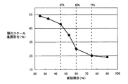
次に、本実施形態によって奏される作用効果を確認すべく、緩和層チップの外径を種々変更することで、貴金属チップの一端面の面積に対する緩和層チップの上面部の面積の割合(面積割合)と、貴金属チップの一端面の外径に対する前記緩和層チップの上面部の外径の割合(直径割合)とを種々変更したスパークプラグのサンプルを作製し、各サンプルについて机上バーナー試験を行った。机上バーナー試験の概要は次の通りである。すなわち、各サンプルの(接地電極側の)貴金属チップの温度が1100℃となるようバーナーで2分間加熱後、1分間徐冷することを1サイクルとして、これを1000サイクル繰り返した。そして、1000サイクル終了後、サンプルの断面を観察し、緩和層チップ等と貴金属チップとの境界面領域の長さに対する、形成された酸化スケールの長さの割合(酸化スケール進展割合)を計測した。図5に、面積割合と、酸化スケール進展割合との関係を表すグラフを示し、図6に、直径割合と、酸化スケール進展割合との関係を表すグラフを示す。 Next, in order to confirm the effects achieved by the present embodiment, the ratio of the area of the upper surface portion of the relaxation layer chip to the area of one end surface of the noble metal chip (area) by variously changing the outer diameter of the relaxation layer chip Ratio) and the ratio of the outer diameter of the upper surface portion of the relaxation layer chip to the outer diameter of one end face of the noble metal chip (diameter ratio) were prepared in various ways, and a desktop burner test was performed on each sample. It was. The outline of the desktop burner test is as follows. That is, heating was performed with a burner for 2 minutes so that the temperature of the noble metal tip (on the ground electrode side) of each sample was 1100 ° C., and then gradually cooling for 1 minute, and this was repeated 1000 cycles. Then, after the end of 1000 cycles, the cross section of the sample was observed, and the ratio of the length of the formed oxide scale to the length of the interface region between the relaxation layer tip and the noble metal tip (oxide scale progress rate) was measured. . FIG. 5 shows a graph showing the relationship between the area ratio and the oxide scale progress rate, and FIG. 6 shows a graph showing the relationship between the diameter ratio and the oxide scale progress rate.
図5及び図6に示すように、面積割合を45%以上としたサンプル(直径割合を68%以上としたサンプル)は、酸化スケール進展割合が50%以下と低減し、貴金属チップの剥離が十分に抑制されることが明らかとなった。これは、緩和層チップが十分なボリュームを備えていたことで、貴金属チップと緩和層チップとの接合部分等において発生する応力を比較的小さくできたことに起因すると考えられる。さらに、面積割合を60%以上としたサンプル(直径割合を77%以上としたサンプル)は、酸化スケール進展割合が30%以下と低減し、貴金属チップの耐剥をより一層抑制できることがわかった。 As shown in FIGS. 5 and 6, the sample with an area ratio of 45% or more (sample with a diameter ratio of 68% or more) has a reduced oxide scale progress rate of 50% or less, and the precious metal tip is sufficiently peeled off. It became clear that it was suppressed. This is considered to be due to the fact that the stress generated at the junction between the noble metal tip and the relaxation layer tip can be made relatively small because the relaxation layer tip has a sufficient volume. Furthermore, it was found that a sample with an area ratio of 60% or more (a sample with a diameter ratio of 77% or more) has a reduced oxide scale progress rate of 30% or less, and can further suppress the resistance to peeling of the noble metal tip.
一方で、面積割合を75%としたサンプル(直径割合を86%としたサンプル)と、面積割合が75%を超えるサンプル(直径割合が86%を超えるサンプル)とを比較した場合には、面積割合(直径割合)が大きいサンプルについて、耐剥離性能の改善が確認されたものの、改善の程度は比較的小さいことがわかった。 On the other hand, when comparing a sample with an area ratio of 75% (sample with a diameter ratio of 86%) and a sample with an area ratio exceeding 75% (a sample with a diameter ratio exceeding 86%), the area Although it was confirmed that the sample with a large ratio (diameter ratio) improved peel resistance, the degree of improvement was found to be relatively small.
以上のように、貴金属チップの耐剥離性能を十分に確保しつつ、緩和層チップを配設するにあたってのコストの増大を抑制するためには、面積割合を45%以上75%以下(直径割合を68%以上86%以下)とした緩和層チップを用いることが有意であるといえる。また、貴金属チップの耐剥離性能の更なる向上を図るという観点からは、面積割合を60%以上75%以下(直径割合を77%以上86%以下)とした緩和層チップを用いることが非常に効果的であるといえる。 As described above, in order to suppress the increase in cost in disposing the relaxation layer tip while sufficiently securing the peeling resistance performance of the noble metal tip, the area ratio is 45% or more and 75% or less (diameter ratio is It can be said that it is significant to use a relaxation layer tip of 68% to 86%). From the viewpoint of further improving the peel resistance of the noble metal tip, it is very preferable to use a relaxation layer tip having an area ratio of 60% to 75% (diameter ratio of 77% to 86%). It can be said that it is effective.
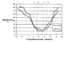
次いで、貴金属チップを接地電極に接合する際のレーザ溶接の条件を変更することで、溶融部における白金の含有量とその他の金属材料の含有量とを種々変更したスパークプラグのサンプルを複数作製し、各サンプルについて上述の机上バーナー試験を行った。そして、1000サイクル終了後、サンプルを樹脂に埋め込んだ上で、貴金属チップの中心軸を含む断面において、溶融部と貴金属チップや接地電極等との境界部分を観察し、当該境界部分において割れの発生した部位の長さを測定するとともに、前記境界部分の長さに対する、当該割れの発生した部位の長さの割合(溶融部割れ割合)を算出した。尚、加熱時においては貴金属チップの温度が950℃となるように加熱をした。また、貴金属チップとしては、Pt−Ni合金からなるもの、又は、Pt−Ir合金からなるものであって、Ptの含有量を50質量%以上100質量%未満の範囲内で変更したものを用いることとした。加えて、サンプルとしては、同一の条件にて形成した机上バーナー試験用のものと組成分析用のものとをそれぞれ用意し、組成分析用のサンプルの溶融部表面をEPMAにより分析することで、溶融部における白金の含有量とその他の金属材料の含有量とを計測した。 Next, by changing the laser welding conditions when joining the noble metal tip to the ground electrode, multiple spark plug samples with various changes in the platinum content and the content of other metal materials in the fusion zone were prepared. The above-described desktop burner test was performed on each sample. After 1000 cycles, the sample is embedded in the resin, and in the cross section including the central axis of the noble metal tip, the boundary portion between the melted portion and the noble metal tip, the ground electrode, etc. is observed, and cracking occurs in the boundary portion. While measuring the length of the part which carried out, the ratio of the length of the part which the said crack generate | occur | produced with respect to the length of the said boundary part (molten part crack ratio) was computed. In addition, it heated so that the temperature of a noble metal tip might be set to 950 degreeC at the time of a heating. Further, as the noble metal tip, one made of a Pt—Ni alloy or one made of a Pt—Ir alloy and having a Pt content changed within a range of 50 mass% or more and less than 100 mass% is used. It was decided. In addition, samples for the desktop burner test and those for composition analysis prepared under the same conditions are prepared, and the melting part surface of the sample for composition analysis is analyzed by EPMA. The platinum content and other metal material content in the part were measured.
図7に、白金の含有量に対するその他の金属材料の含有量の割合(その他金属材料の含有量/白金含有量)と、溶融部割れ割合との関係を表すグラフを示す。尚、図7においては、貴金属チップをPt−Ni合金から形成したサンプルの試験結果を白抜き丸(○)でプロットし、貴金属チップをPt−Ir合金から形成したサンプルの試験結果を白抜き四角(□)でプロットした。 FIG. 7 is a graph showing the relationship between the ratio of the content of other metal materials to the content of platinum (content of other metal materials / platinum content) and the crack ratio of the melted portion. In FIG. 7, the test result of the sample in which the noble metal tip is formed from the Pt—Ni alloy is plotted with a white circle (◯), and the test result of the sample in which the noble metal tip is formed from the Pt—Ir alloy is plotted in the white square. Plotted with (□).
図7に示すように、「その他金属材料の含有量/白金含有量」を3以上10以下としたサンプル、すなわち、溶融部中において、白金の含有量を1とし、その他の金属材料の含有量を3〜10としたサンプルについては、溶融部割れ割合が30%以下となり、溶融部の割れを効果的に抑制できることが明らかとなった。これは、溶融部中における白金の含有量を1とし、その他の金属材料の含有量を3〜10としたことで、溶融部における熱膨張の程度と、接地電極や貴金属チップにおける熱膨張の程度との差を比較的小さなものとすることができたためであると考えられる。 As shown in FIG. 7, a sample having “other metal material content / platinum content” of 3 or more and 10 or less, that is, a platinum content of 1 in the melted portion and a content of other metal materials. For the samples with 3 to 10, the melt crack ratio was 30% or less, and it became clear that cracks in the melt can be effectively suppressed. This is because the content of platinum in the melted part is 1 and the content of other metal materials is 3 to 10, so the degree of thermal expansion in the melted part and the degree of thermal expansion in the ground electrode or noble metal tip This is considered to be because the difference between the two was relatively small.
また特に、溶融部中における白金の含有量を1と、その他の金属材料の含有量を5〜8としたサンプルについては、白金の含有量が種々異なる貴金属チップであっても、溶融部割れ割合が20%以下となり、溶融部の割れを極めて効果的に抑制できることがわかった。 In particular, for samples in which the platinum content in the melted part is 1 and the other metal material content is 5 to 8, even if the platinum content is variously different, the melted part crack ratio It became 20% or less, and it turned out that the crack of a fusion | melting part can be suppressed very effectively.
以上、上記試験の結果を勘案して、溶融部における割れの発生を抑制すべく、前記溶融部中において、白金の含有量を1としたとき、その他の金属材料の含有量を3〜10とすることが好ましく、その他の金属材料の含有量を5〜8とすることがより好ましいといえる。 As mentioned above, in consideration of the result of the above test, in order to suppress the occurrence of cracks in the melted part, when the platinum content in the melted part is 1, the content of other metal materials is 3-10. It is preferable that the content of other metal materials be 5 to 8.
次に、溶融部中における、白金の含有量とその他の金属材料の含有量との比を1:3〜1:10に維持しつつ、レーザビームの照射エネルギー等を変更することで、溶融部の深さ〔すなわち、溶融部のうち最も径方向外側に位置する部位の外径をA(mm)とし、溶融部のうち最も径方向内側に位置する部位の内径をB(mm)としたときにおける、B/Aの値〕を種々変更したスパークプラグのサンプル(サンプル1〜7)を複数作製した。そして、各サンプルについて上述の机上バーナー試験を行い、溶融部割れ割合を算出した。ここで、溶融部割れ割合が30%以下となったサンプルについては、溶融部の割れ抑制効果に優れるとして「○」の評価を下し、一方で、溶融部割れ割合が30%を超えたサンプルについては、溶融部の割れ抑制効果がやや不十分であるとして「△」の評価を下すこととした。表1に、サンプル1〜7の試験結果を示す。
Next, by changing the irradiation energy of the laser beam while maintaining the ratio of the content of platinum and the content of other metal materials in the melted part at 1: 3 to 1:10, the melted part Depth [that is, A (mm) is the outer diameter of the most radially outer portion of the melted portion and B (mm) is the inner diameter of the most radially inner portion of the melted portion. A plurality of spark plug samples (
尚、本試験においては、貴金属チップの加熱温度を1000℃とし、加熱温度を950℃とした上記試験よりもさらに厳しい条件とした。また、貴金属チップとしては、Pt−Ir合金からなるものを用いることとした。 In this test, the heating temperature of the noble metal tip was set to 1000 ° C., and the conditions were more severe than those in the above test in which the heating temperature was 950 ° C. Further, as the noble metal tip, a tip made of a Pt—Ir alloy was used.

従って、当該試験の結果より、溶融部の割れをより確実に抑制するという観点から、溶融部中における白金の含有量とその他の金属材料の含有量との比を1:3〜1:10としつつ、0.45≦B/A≦0.68を満たすように溶融部を形成することが好ましいといえる。 Therefore, from the result of the test, from the viewpoint of more reliably suppressing cracking in the melted portion, the ratio of the platinum content and the other metal material content in the melted portion is set to 1: 3 to 1:10. However, it can be said that it is preferable to form the melted part so as to satisfy 0.45 ≦ B / A ≦ 0.68.
尚、上記実施形態の記載内容に限定されず、例えば次のように実施してもよい。勿論、以下において例示しない他の応用例、変更例も当然可能である。 In addition, it is not limited to the description content of the said embodiment, For example, you may implement as follows. Of course, other application examples and modification examples not illustrated below are also possible.
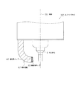
(a)上記実施形態では、貴金属チップ31,33の間に形成された火花放電間隙34において軸線CL1にほぼ沿った方向で火花放電が生じる、いわゆる平行電極タイプのスパークプラグ1において、本発明の技術思想を適用しているが、他のタイプのスパークプラグに対して本発明の技術思想を適用することとしてもよい。従って、例えば、図8に示すように、貴金属チップ63が、接地電極67の先端面に接合された緩和層チップ63と接地電極67とに接合され、軸線CL1とほぼ直交する方向に沿って火花放電が生じるタイプのスパークプラグ102において、本発明の技術思想を適用することとしてもよい。
(A) In the above embodiment, in the so-called parallel electrode
(b)上記実施形態では、溶融部36を設けるにあたって、溶融点36Pの表面が、自身に隣接する溶融点36Pの約30%の領域と重なり合うように形成されているが、図9(a)に示すように、溶融点36Pの表面を、隣接する溶融点36Pの10%程度の領域と重なり合うように形成することとしてもよい。この場合には、レーザ溶接をより効率よく行うことができる。また、図9(b)に示すように、溶融点36Pの表面を、隣接する溶融点36Pの40%以上の領域と重なり合うように形成することとしてもよい。このように溶融点36Pを隣接する溶融点36Pの40%以上の領域と重なり合うように形成することで、接地電極27に対する貴金属チップ33の接合強度の更なる向上を図ることができ、耐剥離性能の一層の向上を図ることができる。 (B) In the above embodiment, when the melting portion 36 is provided, the surface of the melting point 36P is formed so as to overlap with an area of about 30% of the melting point 36P adjacent to the melting point 36P. As shown in FIG. 5, the surface of the melting point 36P may be formed so as to overlap with an area of about 10% of the adjacent melting point 36P. In this case, laser welding can be performed more efficiently. Further, as shown in FIG. 9B, the surface of the melting point 36P may be formed so as to overlap with an area of 40% or more of the adjacent melting point 36P. In this way, by forming the melting point 36P so as to overlap with an area of 40% or more of the adjacent melting point 36P, it is possible to further improve the bonding strength of the noble metal tip 33 to the ground electrode 27, and to prevent peeling. Can be further improved.
(c)上記実施形態では、緩和層チップ32及び貴金属チップ33は円板状をなすように構成されているが、緩和層チップ32や貴金属チップ33の形状はこれに限定されるものではない。従って、例えば、図10に示すように、円板状の貴金属チップ73を用いる一方で、緩和層チップ72(同図、破線で示した部位)として、断面矩形状をなすものを用いることとしてもよい。 (C) In the above embodiment, the relaxing layer chip 32 and the noble metal tip 33 are configured to have a disk shape, but the shapes of the relaxing layer chip 32 and the noble metal tip 33 are not limited thereto. Therefore, for example, as shown in FIG. 10, while using a disc-shaped noble metal tip 73, it is also possible to use a relaxation layer tip 72 (part indicated by a broken line in the same figure) having a rectangular cross section. Good.
(d)上記実施形態では、接地電極27に緩和層チップ32を抵抗溶接するにあたって、平坦状の側面27Fに対して緩和層チップ32が抵抗溶接されているが、図11(a),(b)に示すように、接地電極27のうち前記貴金属チップ31との対向予定位置に接合穴41を設け、当該接合穴41に緩和層チップ32を配置した上で、接地電極27に対して緩和層チップ32を抵抗溶接することとしてもよい。尚、この場合において、接合穴41の内径は、緩和層チップ32の外径よりも一回り大きいものとすることが好ましい。このように接合穴41の内径を、緩和層チップ32の外径よりも一回り大きくすれば、接合穴41の底部と緩和層チップ32の下面部との間に十分な溶融エネルギーを供給することができ、ひいては緩和層チップ32を接地電極27に対して強固に接合することができる。また、接合穴41を比較的大きく形成することで、接合穴41に対する緩和層チップ32の配置作業の容易化を図ることができる。尚、緩和層チップ32と接合穴41の側壁との間に形成される環状の間隙については、接地電極27を構成するNi合金等がレーザ溶接等により溶融することで埋まることとなる。
(D) In the above embodiment, when the relaxation layer tip 32 is resistance welded to the ground electrode 27, the relaxation layer tip 32 is resistance welded to the
(e)上記実施形態では、レーザ溶接によって貴金属チップ33の他端面33Aが溶融し、当該他端面33Aの外周部分に角部33Eが形成されているが、図12に示すように、レーザビームの照射エネルギーや照射角度を変更することによって貴金属チップ33の他端面33Aに角部33Eが形成されないようにレーザ溶接することとしてもよい。
(E) In the above embodiment, the
(f)上記実施形態では特に言及していないが、緩和層チップ32の中心軸と貴金属チップ33の中心軸とが一致するようにして両者を配設することとしてもよい。 (F) Although not specifically mentioned in the above embodiment, both may be arranged such that the central axis of the relaxation layer tip 32 and the central axis of the noble metal tip 33 coincide.
(g)上記実施形態では、中心電極5の先端部には貴金属チップ31が設けられているが、当該貴金属チップ31を省略して構成することとしてもよい。
(G) In the above embodiment, the
(h)上記実施形態では、主体金具3の先端面に、接地電極27が接合される場合について具体化しているが、主体金具の一部(又は、主体金具に予め溶接してある先端金具の一部)を削り出すようにして接地電極を形成する場合についても適用可能である(例えば、特開2006−236906号公報等)。また、主体金具3の先端部26の側面に接地電極27を接合することとしてもよい。
(H) In the above embodiment, the case where the ground electrode 27 is joined to the front end surface of the
(i)上記実施形態では、工具係合部19は断面六角形状とされているが、工具係合部19の形状に関しては、このような形状に限定されるものではない。例えば、Bi−HEX(変形12角)形状〔ISO22977:2005(E)〕等とされていてもよい。
(I) In the above embodiment, the
(j)上記実施形態におけるスパークプラグ1は、主としてガスエンジン等の使用条件の厳しいエンジンに用いられるものであるが、本発明の技術思想を、自動車用のガソリンエンジン等に適用することとしてもよい。この場合においても、貴金属チップ33の耐剥離性の向上や、緩和層チップ32を設けたことに伴うコストの増大を効果的に抑制することができる。
(J) The
1…スパークプラグ(内燃機関用スパークプラグ)
2…絶縁碍子(絶縁体)
3…主体金具
4…軸孔
5…中心電極
27,67…接地電極
32,62,72…緩和層チップ
33,63,73…貴金属チップ
33A…他端面
33B…一端面
34…火花放電間隙(間隙)
36…溶融部
36P…溶融点(溶融領域)
CL1…軸線1 ... Spark plug (spark plug for internal combustion engine)
2. Insulator (insulator)
3 ... metal shell 4 ...
36 ... Melting part 36P ... Melting point (melting region)
CL1 ... axis
Claims (10)
前記軸孔に設けられた棒状の中心電極と、
前記絶縁体の外周に設けられた円筒状の主体金具と、
前記主体金具の先端部から延び、前記中心電極に向けて曲げられて配置された接地電極と、
前記接地電極の先端部に埋設された状態で抵抗溶接された板状の緩和層チップと、
前記緩和層チップの中心電極側の部位、及び、前記接地電極のうち前記緩和層チップの中心電極側の部位の外周側の部位に抵抗溶接される一端面、及び、前記中心電極の先端部との間で間隙を形成する他端面を有する貴金属チップとを備えた内燃機関用スパークプラグであって、
前記貴金属チップは、白金を主成分とする白金合金からなるとともに、
前記緩和層チップは、前記貴金属チップを形成する白金合金と、前記接地電極を形成する金属材料との間の線膨張係数を有する白金合金からなり、
前記緩和層チップのうち前記貴金属チップに接合される部位の面積が、前記貴金属チップの一端面の面積よりも小さく、かつ、
前記接地電極と、前記貴金属チップとの境界部の外周部分の全域に、少なくとも前記貴金属チップと前記接地電極とがレーザ溶接によって溶融されてなる溶融部が設けられていることを特徴とする内燃機関用スパークプラグ。An insulator having an axial hole extending in the axial direction;
A rod-shaped center electrode provided in the shaft hole;
A cylindrical metal shell provided on the outer periphery of the insulator;
A ground electrode that extends from the tip of the metal shell and is bent toward the center electrode; and
A plate-shaped relaxation layer tip resistance-welded in a state embedded in the tip of the ground electrode;
A portion of the relaxation layer tip on the center electrode side, and one end surface of the ground electrode that is resistance-welded to a portion on the outer peripheral side of the portion on the center electrode side of the relaxation layer tip, and a tip portion of the center electrode A spark plug for an internal combustion engine comprising a noble metal tip having a second end surface that forms a gap therebetween,
The noble metal tip is made of a platinum alloy mainly composed of platinum,
The relaxation layer tip is made of a platinum alloy having a linear expansion coefficient between a platinum alloy forming the noble metal tip and a metal material forming the ground electrode,
The area of the part to be joined to the noble metal tip of the relaxation layer tip is smaller than the area of one end surface of the noble metal tip, and
An internal combustion engine characterized in that a melted portion in which at least the noble metal tip and the ground electrode are melted by laser welding is provided over the entire outer peripheral portion of the boundary portion between the ground electrode and the noble metal tip. For spark plug.
前記緩和層チップのうち前記貴金属チップに抵抗溶接される部位の外径は、前記貴金属チップの一端面の外径の68%以上86%以下であることを特徴とする請求項1乃至3のいずれか1項に記載の内燃機関用スパークプラグ。The relaxation layer tip and the noble metal tip have a disk shape,
4. The outer diameter of a portion of the relaxation layer tip that is resistance-welded to the noble metal tip is 68% or more and 86% or less of an outer diameter of one end face of the noble metal tip. A spark plug for an internal combustion engine according to claim 1.
前記緩和層チップのうち前記貴金属チップに抵抗溶接される部位の外径は、前記貴金属チップの一端面の外径の77%以上86%以下であることを特徴とする請求項1乃至4のいずれか1項に記載の内燃機関用スパークプラグ。The relaxation layer tip and the noble metal tip have a disk shape,
5. The outer diameter of a portion of the relaxation layer tip that is resistance-welded to the noble metal tip is 77% or more and 86% or less of the outer diameter of one end face of the noble metal tip. A spark plug for an internal combustion engine according to claim 1.
前記接地電極に対する前記貴金属チップの埋め込み量を、埋め込み前の前記貴金属チップの高さの25%以下としたことを特徴とする請求項1乃至6のいずれか1項に記載の内燃機関用スパークプラグ。The noble metal tip is melt-bonded with one end portion embedded in the ground electrode,
The spark plug for an internal combustion engine according to any one of claims 1 to 6, wherein an amount of the noble metal tip embedded in the ground electrode is 25% or less of a height of the noble metal tip before being embedded. .
前記溶融部のうち最も径方向内側に位置する部位の内径をB(mm)としたとき、
0.45≦B/A≦0.68
を満たすことを特徴とする請求項8に記載の内燃機関用スパークプラグ。The outer diameter of the portion located on the outermost radial direction in the melted portion is A (mm),
When the inner diameter of the portion located on the radially inner side of the melted portion is B (mm),
0.45 ≦ B / A ≦ 0.68
The spark plug for an internal combustion engine according to claim 8, wherein:
前記各溶融領域の表面は、自身に隣接する溶融領域の20%以上60%以下の領域で重なり合って形成されることを特徴とする請求項1乃至9のいずれか1項に記載の内燃機関用スパークプラグ。The melting part is formed by linking a plurality of melting regions formed by irradiating a laser beam,
10. The internal combustion engine according to claim 1, wherein the surface of each melting region is formed so as to overlap in a region of 20% to 60% of a melting region adjacent to the melting region. Spark plug.
Priority Applications (1)
| Application Number | Priority Date | Filing Date | Title |
|---|---|---|---|
| JP2010515143A JP5092012B2 (en) | 2008-11-21 | 2009-11-20 | Spark plug for internal combustion engine |
Applications Claiming Priority (4)
| Application Number | Priority Date | Filing Date | Title |
|---|---|---|---|
| JP2008297478 | 2008-11-21 | ||
| JP2008297478 | 2008-11-21 | ||
| JP2010515143A JP5092012B2 (en) | 2008-11-21 | 2009-11-20 | Spark plug for internal combustion engine |
| PCT/JP2009/069695 WO2010058835A1 (en) | 2008-11-21 | 2009-11-20 | Spark plug for internal combustion engine |
Publications (2)
| Publication Number | Publication Date |
|---|---|
| JPWO2010058835A1 JPWO2010058835A1 (en) | 2012-04-19 |
| JP5092012B2 true JP5092012B2 (en) | 2012-12-05 |
Family
ID=42198274
Family Applications (1)
| Application Number | Title | Priority Date | Filing Date |
|---|---|---|---|
| JP2010515143A Active JP5092012B2 (en) | 2008-11-21 | 2009-11-20 | Spark plug for internal combustion engine |
Country Status (4)
| Country | Link |
|---|---|
| US (1) | US8648519B2 (en) |
| EP (1) | EP2348590B1 (en) |
| JP (1) | JP5092012B2 (en) |
| WO (1) | WO2010058835A1 (en) |
Cited By (1)
| Publication number | Priority date | Publication date | Assignee | Title |
|---|---|---|---|---|
| US10312669B2 (en) | 2016-01-26 | 2019-06-04 | Ngk Spark Plug Co., Ltd. | Spark plug |
Families Citing this family (12)
| Publication number | Priority date | Publication date | Assignee | Title |
|---|---|---|---|---|
| JP5406982B2 (en) * | 2010-11-17 | 2014-02-05 | 日本特殊陶業株式会社 | Spark plug |
| DE102013105698B4 (en) | 2012-06-01 | 2019-05-02 | Federal-Mogul Ignition Company | spark plug |
| US9673593B2 (en) | 2012-08-09 | 2017-06-06 | Federal-Mogul Ignition Company | Spark plug having firing pad |
| US9318879B2 (en) | 2012-10-19 | 2016-04-19 | Federal-Mogul Ignition Company | Spark plug having firing pad |
| US9231379B2 (en) | 2013-01-31 | 2016-01-05 | Federal-Mogul Ignition Company | Spark plug having firing pad |
| US9041274B2 (en) | 2013-01-31 | 2015-05-26 | Federal-Mogul Ignition Company | Spark plug having firing pad |
| US9368943B2 (en) * | 2013-03-12 | 2016-06-14 | Federal-Mogul Ignition Company | Spark plug having multi-layer sparking component attached to ground electrode |
| JP5890368B2 (en) * | 2013-10-11 | 2016-03-22 | 日本特殊陶業株式会社 | Spark plug |
| JP5995912B2 (en) * | 2014-06-04 | 2016-09-21 | 日本特殊陶業株式会社 | Spark plug and method of manufacturing spark plug |
| JP6320354B2 (en) | 2015-09-01 | 2018-05-09 | 日本特殊陶業株式会社 | Spark plug and manufacturing method thereof |
| JP6105694B2 (en) * | 2015-09-04 | 2017-03-29 | 日本特殊陶業株式会社 | Spark plug |
| DE102018101512B4 (en) | 2018-01-24 | 2020-03-19 | Federal-Mogul Ignition Gmbh | Method of making an electrode assembly, electrode assembly, and spark plug |
Citations (2)
| Publication number | Priority date | Publication date | Assignee | Title |
|---|---|---|---|---|
| JPH11329668A (en) * | 1998-05-20 | 1999-11-30 | Denso Corp | Spark plug |
| JP2004288376A (en) * | 2003-03-19 | 2004-10-14 | Ngk Spark Plug Co Ltd | Spark plug and manufacturing method of spark plug |
Family Cites Families (11)
| Publication number | Priority date | Publication date | Assignee | Title |
|---|---|---|---|---|
| JPS5940482A (en) | 1982-08-30 | 1984-03-06 | 日本特殊陶業株式会社 | Spark plug |
| US6346766B1 (en) * | 1998-05-20 | 2002-02-12 | Denso Corporation | Spark plug for internal combustion engine and method for manufacturing same |
| JP2001273966A (en) * | 2000-01-18 | 2001-10-05 | Denso Corp | Spark plug |
| WO2001054242A1 (en) * | 2000-01-19 | 2001-07-26 | Ngk Spark Plug Co., Ltd. | Spark plug for internal combustion engine |
| JP2001273965A (en) * | 2000-01-19 | 2001-10-05 | Ngk Spark Plug Co Ltd | Spark plug for internal combustion engine |
| DE60106430T2 (en) * | 2001-08-23 | 2006-02-02 | Federal-Mogul S.A. | Spark plug for internal combustion engine |
| WO2004107517A1 (en) * | 2003-05-28 | 2004-12-09 | Ngk Spark Plug Co., Ltd. | Spark plug |
| JP2006236906A (en) | 2005-02-28 | 2006-09-07 | Ngk Spark Plug Co Ltd | Manufacturing method of spark plug |
| JP2008077838A (en) * | 2006-09-18 | 2008-04-03 | Denso Corp | Spark plug for internal combustion engine, and manufacturing method therefor |
| WO2009081562A1 (en) * | 2007-12-20 | 2009-07-02 | Ngk Spark Plug Co., Ltd. | Spark plug and process for producing the spark plug |
| JP4705129B2 (en) * | 2008-05-21 | 2011-06-22 | 日本特殊陶業株式会社 | Spark plug |
-
2009
- 2009-11-20 JP JP2010515143A patent/JP5092012B2/en active Active
- 2009-11-20 WO PCT/JP2009/069695 patent/WO2010058835A1/en active Application Filing
- 2009-11-20 US US12/998,301 patent/US8648519B2/en active Active
- 2009-11-20 EP EP09827616.5A patent/EP2348590B1/en active Active
Patent Citations (2)
| Publication number | Priority date | Publication date | Assignee | Title |
|---|---|---|---|---|
| JPH11329668A (en) * | 1998-05-20 | 1999-11-30 | Denso Corp | Spark plug |
| JP2004288376A (en) * | 2003-03-19 | 2004-10-14 | Ngk Spark Plug Co Ltd | Spark plug and manufacturing method of spark plug |
Cited By (1)
| Publication number | Priority date | Publication date | Assignee | Title |
|---|---|---|---|---|
| US10312669B2 (en) | 2016-01-26 | 2019-06-04 | Ngk Spark Plug Co., Ltd. | Spark plug |
Also Published As
| Publication number | Publication date |
|---|---|
| US8648519B2 (en) | 2014-02-11 |
| WO2010058835A1 (en) | 2010-05-27 |
| JPWO2010058835A1 (en) | 2012-04-19 |
| EP2348590A4 (en) | 2013-04-03 |
| EP2348590A1 (en) | 2011-07-27 |
| EP2348590B1 (en) | 2018-05-02 |
| US20110198981A1 (en) | 2011-08-18 |
Similar Documents
| Publication | Publication Date | Title |
|---|---|---|
| JP5092012B2 (en) | Spark plug for internal combustion engine | |
| JP4928596B2 (en) | Spark plug and manufacturing method thereof | |
| JP5341752B2 (en) | Spark plug for internal combustion engine and method for manufacturing the same | |
| JP4617388B1 (en) | Spark plug | |
| JP4402731B2 (en) | Spark plug for internal combustion engine and method of manufacturing spark plug | |
| JP5044665B2 (en) | Spark plug | |
| JP5048063B2 (en) | Spark plug for internal combustion engine | |
| JP5200013B2 (en) | Spark plug for internal combustion engine | |
| JP4644291B2 (en) | Spark plug for internal combustion engine and method for manufacturing the same | |
| JP5022465B2 (en) | Spark plug for internal combustion engine and method for manufacturing the same | |
| EP2560255A1 (en) | Spark plug for internal combustion engine and method of manufacturing spark plug | |
| JPWO2013179640A1 (en) | Gasket, manufacturing method thereof, spark plug, and manufacturing method thereof | |
| JP2008053018A (en) | Spark plug for internal combustion engine | |
| JP4426614B2 (en) | Spark plug for internal combustion engine | |
| JP2015022791A (en) | Spark plug and method of manufacturing the same | |
| JP5054633B2 (en) | Spark plug for internal combustion engine | |
| JP5167336B2 (en) | Spark plug | |
| JP5331179B2 (en) | Manufacturing method of spark plug | |
| JP5449114B2 (en) | Spark plug and manufacturing method thereof | |
| JP6069082B2 (en) | Spark plug and manufacturing method thereof | |
| JP5337057B2 (en) | Spark plug | |
| JP2008103147A (en) | Spark plug for internal combustion engine |
Legal Events
| Date | Code | Title | Description |
|---|---|---|---|
| TRDD | Decision of grant or rejection written | ||
| A01 | Written decision to grant a patent or to grant a registration (utility model) |
Free format text: JAPANESE INTERMEDIATE CODE: A01 Effective date: 20120821 |
|
| A01 | Written decision to grant a patent or to grant a registration (utility model) |
Free format text: JAPANESE INTERMEDIATE CODE: A01 |
|
| A61 | First payment of annual fees (during grant procedure) |
Free format text: JAPANESE INTERMEDIATE CODE: A61 Effective date: 20120914 |
|
| FPAY | Renewal fee payment (event date is renewal date of database) |
Free format text: PAYMENT UNTIL: 20150921 Year of fee payment: 3 |
|
| R150 | Certificate of patent or registration of utility model |
Ref document number: 5092012 Country of ref document: JP Free format text: JAPANESE INTERMEDIATE CODE: R150 Free format text: JAPANESE INTERMEDIATE CODE: R150 |
|
| R250 | Receipt of annual fees |
Free format text: JAPANESE INTERMEDIATE CODE: R250 |
|
| R250 | Receipt of annual fees |
Free format text: JAPANESE INTERMEDIATE CODE: R250 |
|
| R250 | Receipt of annual fees |
Free format text: JAPANESE INTERMEDIATE CODE: R250 |
|
| R250 | Receipt of annual fees |
Free format text: JAPANESE INTERMEDIATE CODE: R250 |
|
| R250 | Receipt of annual fees |
Free format text: JAPANESE INTERMEDIATE CODE: R250 |
|
| R250 | Receipt of annual fees |
Free format text: JAPANESE INTERMEDIATE CODE: R250 |
|
| R250 | Receipt of annual fees |
Free format text: JAPANESE INTERMEDIATE CODE: R250 |
|
| R250 | Receipt of annual fees |
Free format text: JAPANESE INTERMEDIATE CODE: R250 |
|
| S531 | Written request for registration of change of domicile |
Free format text: JAPANESE INTERMEDIATE CODE: R313531 |
|
| R350 | Written notification of registration of transfer |
Free format text: JAPANESE INTERMEDIATE CODE: R350 |
|
| R250 | Receipt of annual fees |
Free format text: JAPANESE INTERMEDIATE CODE: R250 |