JP5085902B2 - Manufacturing method of display device - Google Patents
Manufacturing method of display device Download PDFInfo
- Publication number
- JP5085902B2 JP5085902B2 JP2006227265A JP2006227265A JP5085902B2 JP 5085902 B2 JP5085902 B2 JP 5085902B2 JP 2006227265 A JP2006227265 A JP 2006227265A JP 2006227265 A JP2006227265 A JP 2006227265A JP 5085902 B2 JP5085902 B2 JP 5085902B2
- Authority
- JP
- Japan
- Prior art keywords
- continuous wave
- wave laser
- region
- manufacturing
- substrate
- Prior art date
- Legal status (The legal status is an assumption and is not a legal conclusion. Google has not performed a legal analysis and makes no representation as to the accuracy of the status listed.)
- Expired - Fee Related
Links
Images


Classifications
-
- H—ELECTRICITY
- H01—ELECTRIC ELEMENTS
- H01L—SEMICONDUCTOR DEVICES NOT COVERED BY CLASS H10
- H01L21/00—Processes or apparatus adapted for the manufacture or treatment of semiconductor or solid state devices or of parts thereof
- H01L21/02—Manufacture or treatment of semiconductor devices or of parts thereof
- H01L21/02104—Forming layers
- H01L21/02365—Forming inorganic semiconducting materials on a substrate
- H01L21/02518—Deposited layers
- H01L21/02521—Materials
- H01L21/02524—Group 14 semiconducting materials
- H01L21/02532—Silicon, silicon germanium, germanium
-
- H—ELECTRICITY
- H01—ELECTRIC ELEMENTS
- H01L—SEMICONDUCTOR DEVICES NOT COVERED BY CLASS H10
- H01L21/00—Processes or apparatus adapted for the manufacture or treatment of semiconductor or solid state devices or of parts thereof
- H01L21/02—Manufacture or treatment of semiconductor devices or of parts thereof
- H01L21/02104—Forming layers
- H01L21/02365—Forming inorganic semiconducting materials on a substrate
- H01L21/02656—Special treatments
- H01L21/02664—Aftertreatments
- H01L21/02667—Crystallisation or recrystallisation of non-monocrystalline semiconductor materials, e.g. regrowth
- H01L21/02675—Crystallisation or recrystallisation of non-monocrystalline semiconductor materials, e.g. regrowth using laser beams
- H01L21/02683—Continuous wave laser beam
-
- H—ELECTRICITY
- H01—ELECTRIC ELEMENTS
- H01L—SEMICONDUCTOR DEVICES NOT COVERED BY CLASS H10
- H01L21/00—Processes or apparatus adapted for the manufacture or treatment of semiconductor or solid state devices or of parts thereof
- H01L21/02—Manufacture or treatment of semiconductor devices or of parts thereof
- H01L21/02104—Forming layers
- H01L21/02365—Forming inorganic semiconducting materials on a substrate
- H01L21/02656—Special treatments
- H01L21/02664—Aftertreatments
- H01L21/02667—Crystallisation or recrystallisation of non-monocrystalline semiconductor materials, e.g. regrowth
- H01L21/02691—Scanning of a beam
-
- H—ELECTRICITY
- H01—ELECTRIC ELEMENTS
- H01L—SEMICONDUCTOR DEVICES NOT COVERED BY CLASS H10
- H01L27/00—Devices consisting of a plurality of semiconductor or other solid-state components formed in or on a common substrate
- H01L27/02—Devices consisting of a plurality of semiconductor or other solid-state components formed in or on a common substrate including semiconductor components specially adapted for rectifying, oscillating, amplifying or switching and having at least one potential-jump barrier or surface barrier; including integrated passive circuit elements with at least one potential-jump barrier or surface barrier
- H01L27/12—Devices consisting of a plurality of semiconductor or other solid-state components formed in or on a common substrate including semiconductor components specially adapted for rectifying, oscillating, amplifying or switching and having at least one potential-jump barrier or surface barrier; including integrated passive circuit elements with at least one potential-jump barrier or surface barrier the substrate being other than a semiconductor body, e.g. an insulating body
- H01L27/1214—Devices consisting of a plurality of semiconductor or other solid-state components formed in or on a common substrate including semiconductor components specially adapted for rectifying, oscillating, amplifying or switching and having at least one potential-jump barrier or surface barrier; including integrated passive circuit elements with at least one potential-jump barrier or surface barrier the substrate being other than a semiconductor body, e.g. an insulating body comprising a plurality of TFTs formed on a non-semiconducting substrate, e.g. driving circuits for AMLCDs
- H01L27/1259—Multistep manufacturing methods
- H01L27/127—Multistep manufacturing methods with a particular formation, treatment or patterning of the active layer specially adapted to the circuit arrangement
- H01L27/1274—Multistep manufacturing methods with a particular formation, treatment or patterning of the active layer specially adapted to the circuit arrangement using crystallisation of amorphous semiconductor or recrystallisation of crystalline semiconductor
- H01L27/1285—Multistep manufacturing methods with a particular formation, treatment or patterning of the active layer specially adapted to the circuit arrangement using crystallisation of amorphous semiconductor or recrystallisation of crystalline semiconductor using control of the annealing or irradiation parameters, e.g. using different scanning direction or intensity for different transistors
Description
本発明は、表示装置の製造方法に関し、特に、TFT素子を有する画素の集合からなる表示領域の外側に半導体素子を有する駆動回路を形成する製造方法に適用して有効な技術に関するものである。 The present invention relates to a method for manufacturing a display device, and more particularly to a technique effective when applied to a manufacturing method for forming a drive circuit having a semiconductor element outside a display region composed of a set of pixels having TFT elements.
従来、一対の基板の間に液晶材料を封入した液晶表示パネルを有する液晶表示装置には、アクティブマトリクス型のTFT液晶表示装置がある。アクティブマトリクス型のTFT液晶表示装置は、たとえば、テレビ受像器やパーソナル・コンピュータ(PC)のディスプレイ、携帯電話端末や携帯情報端末(PDA)の表示部などに広く用いられている。 Conventionally, a liquid crystal display device having a liquid crystal display panel in which a liquid crystal material is sealed between a pair of substrates includes an active matrix TFT liquid crystal display device. An active matrix TFT liquid crystal display device is widely used, for example, in a television receiver, a display of a personal computer (PC), a display unit of a mobile phone terminal or a personal digital assistant (PDA).
アクティブマトリクス型のTFT液晶表示装置で用いられる液晶表示パネルは、一方の基板に、複数本の走査信号線、複数本の映像信号線、TFT素子、画素電極などが設けられている。 In a liquid crystal display panel used in an active matrix TFT liquid crystal display device, a plurality of scanning signal lines, a plurality of video signal lines, TFT elements, pixel electrodes, and the like are provided on one substrate.
従来の液晶表示装置は、たとえば、複数本の映像信号線に映像信号(階調データと呼ぶこともある)を入力するためのドライバICや、複数本の走査信号線に走査信号を入力するためのドライバICが実装されたTCPやCOFなどのフレキシブル回路基板を液晶表示パネルに接続したり、前記各ドライバICを直接液晶表示パネル上に実装しているのが一般的である。 In a conventional liquid crystal display device, for example, a driver IC for inputting a video signal (sometimes referred to as gradation data) to a plurality of video signal lines or a scanning signal to a plurality of scanning signal lines is input. In general, a flexible circuit board such as TCP or COF on which a driver IC is mounted is connected to a liquid crystal display panel, or each of the driver ICs is mounted directly on the liquid crystal display panel.
また、近年は、たとえば、前記走査信号線などが形成された基板(以下、TFT基板と呼ぶ)の表示領域の外側に、前記ドライバICと同等の機能を有する駆動回路(周辺回路)を形成した液晶表示パネルが提案されている。 In recent years, for example, a drive circuit (peripheral circuit) having a function equivalent to that of the driver IC is formed outside a display region of a substrate (hereinafter referred to as a TFT substrate) on which the scanning signal lines are formed. Liquid crystal display panels have been proposed.
前記TFT基板の表示領域の外側に形成される前記駆動回路は、主に、トランジスタやダイオードなどの半導体素子で構成されており、前記走査信号線や前記映像信号線を形成する際に各半導体素子の電極を形成し、表示領域のTFT素子の半導体層(チャネル層)を形成する際に半導体素子の半導体層を形成する。TFT基板の表示領域に形成するTFT素子の半導体層には、たとえば、アモルファスシリコン(a−Si)または多結晶シリコン(poly−Si)が用いられる。 The drive circuit formed outside the display area of the TFT substrate is mainly composed of semiconductor elements such as transistors and diodes, and each semiconductor element is formed when forming the scanning signal lines and the video signal lines. The semiconductor layer of the semiconductor element is formed when the semiconductor layer (channel layer) of the TFT element in the display region is formed. For example, amorphous silicon (a-Si) or polycrystalline silicon (poly-Si) is used for the semiconductor layer of the TFT element formed in the display region of the TFT substrate.
ところで、前記駆動回路の半導体素子の半導体層は、動作特性の面から、多結晶シリコンを用いることが望ましい。このとき、一般的には、熱処理によりアモルファスシリコンを脱水素化し、脱水素化したアモルファスシリコンに対してエキシマレーザなどのパルスレーザを1箇所に対して複数回照射されるように少しずつステップ移動させて照射および走査することで、基板上のアモルファスシリコンの全面を多結晶化する方法が採用されている。 By the way, it is desirable that the semiconductor layer of the semiconductor element of the drive circuit is made of polycrystalline silicon from the viewpoint of operating characteristics. At this time, in general, the amorphous silicon is dehydrogenated by heat treatment, and the dehydrogenated amorphous silicon is stepped little by little so that a pulse laser such as an excimer laser is irradiated multiple times to one place. A method of polycrystallizing the entire surface of amorphous silicon on the substrate by irradiating and scanning is employed.
また、熱処理の代わりに、レーザビームを用いてアモルファスシリコンを脱水素化する方法が、たとえば、特許文献1や特許文献2に開示されている。特許文献1では、第1のエキシマレーザで脱水素化を行い、第2のエキシマレーザで多結晶化を行っている。また、特許文献2では、パルスレーザビームを2分割し、先行するビームで脱水素化を行い、それに続くビームで多結晶化を行っている。
Further, for example,
また、脱水素を目的としたものではないが、2つのレーザを用いることに関連して、特許文献3には、エネルギー密度の異なる2つのレーザでアニールを行うことが開示されており、その2つのレーザには、パルスレーザまたは連続発振レーザを用いている。
Although not intended for dehydrogenation, in connection with the use of two lasers,
またさらに、アモルファスシリコン膜の全面を多結晶化するのではなく、駆動回路部のみを多結晶化する方法が、特許文献4に開示されている。特許文献4では、画素を水素化アモルファスシリコン、駆動回路を多結晶シリコンで構成する際に、1つのパルスレーザを用い、レーザ光のパルスのエネルギーを段階的に大きくしていき、駆動回路部のみ、水素化非晶質半導体の脱水素化を行いながら結晶化を行っている。
ここで、表示領域のTFT素子の半導体層はアモルファスシリコンを用い、表示領域の外側の駆動回路の半導体素子の半導体層は多結晶シリコンを用いたTFT基板を製造するときには、アモルファスシリコンは水素化したアモルファスシリコンを用いるのが特性上好ましいが、多結晶化する際には脱水素化を行わないと、レーザを照射したときに突沸してしまうので、駆動回路部分のみを部分的に脱水素化する必要がある。 Here, when manufacturing a TFT substrate using amorphous silicon for the semiconductor layer of the TFT element in the display region and using polycrystalline silicon for the semiconductor layer of the semiconductor element of the driving circuit outside the display region, the amorphous silicon was hydrogenated. Amorphous silicon is preferable in terms of characteristics, but if dehydrogenation is not performed when polycrystallizing, bumping occurs when irradiated with laser, so only the drive circuit portion is partially dehydrogenated. There is a need.
しかしながら、特許文献1、特許文献2、特許文献4では、部分的に脱水素化をしている領域と結晶化をしている領域は完全に一致しているため、結晶化を行うためのレーザを照射するときに照射位置がずれた場合には、脱水素化した領域と脱水素化していない領域との境界部分で、脱水素化していない領域に結晶化のためのレーザが照射される可能性があり、その結果、突沸が発生する可能性がある。
However, in
なお、特許文献3には、脱水素化に関しては記載されていないが、2つのレーザの照射領域は一致しているため、脱水素化と結晶化に応用しようとした場合には、同様の問題が発生すると考えられる。
Although
また、パルスレーザは、ある時間間隔で断続的に発光(発生)するレーザである。そのため、パルスレーザを照射してアモルファスシリコンを溶融、結晶化して多結晶化した場合、個々の粒状結晶の大きさが小さく、結晶粒界が多いという問題があった。その結果、たとえば、前記駆動回路のTFT素子におけるキャリアの移動度が低く、十分なトランジスタ特性を得られないという問題が生じる。 The pulse laser is a laser that emits light (generates) intermittently at certain time intervals. For this reason, when amorphous silicon is melted and crystallized by irradiating a pulsed laser, the size of each granular crystal is small and there are many crystal grain boundaries. As a result, for example, the carrier mobility in the TFT element of the drive circuit is low, and there is a problem that sufficient transistor characteristics cannot be obtained.
本発明の目的は、基板の表示領域の外側にあるアモルファスシリコンを脱水素化、多結晶シリコン化させる際の、多結晶シリコンの質を向上させることが可能な技術を提供することにある。 An object of the present invention is to provide a technique capable of improving the quality of polycrystalline silicon when amorphous silicon existing outside a display region of a substrate is dehydrogenated to polycrystalline silicon.
本発明の他の目的は、表示領域のTFT素子の半導体層にはアモルファスシリコンを用い、表示領域の外側にある駆動回路の半導体素子の半導体層には多結晶シリコンを用いたTFT基板の製造効率を向上させることが可能な技術を提供することにある。 Another object of the present invention is to produce a TFT substrate using amorphous silicon for the semiconductor layer of the TFT element in the display region and using polycrystalline silicon for the semiconductor layer of the semiconductor element of the drive circuit outside the display region. It is to provide a technology capable of improving the quality.
本発明の前記ならびにその他の目的と新規な特徴は、本明細書の記述および添付図面によって明らかになるであろう。 The above and other objects and novel features of the present invention will be apparent from the description of this specification and the accompanying drawings.
本願において開示される発明のうち、代表的なものの概略を説明すれば、以下の通りである。 The outline of typical inventions among the inventions disclosed in the present application will be described as follows.
(1)基板の上に水素化したアモルファスシリコン膜を成膜する第1の工程と、前記水素化したアモルファスシリコン膜のあらかじめ定められた領域を脱水素化した後、前記脱水素化された領域のアモルファスシリコンを溶融、結晶化して多結晶シリコンにする第2の工程とを有し、前記基板の表示領域にアモルファスシリコンを用いたTFT素子を有する複数の画素を形成するとともに、該表示領域の外側に、多結晶シリコンを用いた複数個の半導体素子を有する駆動回路を形成する表示装置の製造方法であって、前記第2の工程は、前記基板の前記表示領域の外側にある前記駆動回路を形成する領域およびその周辺領域のみを第1の連続発振レーザを照射して脱水素化した後、前記脱水素化された領域のみに第2の連続発振レーザを照射して前記アモルファスシリコンを前記多結晶シリコンにし、前記第1の連続発振レーザを照射する領域は、前記第2の連続発振レーザを照射する領域よりも広い表示装置の製造方法。 (1) a first step of forming a hydrogenated amorphous silicon film on a substrate; and a predetermined region of the hydrogenated amorphous silicon film is dehydrogenated and then the dehydrogenated region A second step of melting and crystallizing the amorphous silicon to form polycrystalline silicon, forming a plurality of pixels having TFT elements using amorphous silicon in the display region of the substrate, A method of manufacturing a display device, wherein a driving circuit having a plurality of semiconductor elements using polycrystalline silicon is formed on the outside, wherein the second step is the driving circuit outside the display area of the substrate. The first continuous wave laser is irradiated to only the region forming the region and its peripheral region, and then the second continuous wave laser is irradiated only to the dehydrogenated region. It said amorphous silicon into the polycrystalline silicon, the first region to be irradiated with continuous wave laser of the manufacturing method of a wide display device than the area to be irradiated with the second continuous oscillation laser Te.
(2)前記(1)の表示装置の製造方法において、前記第1の連続発振レーザおよび前記第2の連続発振レーザは、前記基板の上を走査しながら照射し、前記第1の連続発振レーザのエネルギー密度は、前記第2の連続発振レーザのエネルギー密度よりも低く、前記第1の連続発振レーザおよび前記第2の連続発振レーザが照射する領域の各点は、前記第1の連続発振レーザが照射されている時間が、前記第2の連続発振レーザが照射されている時間よりも長い表示装置の製造方法。 (2) In the method for manufacturing a display device according to (1), the first continuous wave laser and the second continuous wave laser are irradiated while scanning over the substrate, and the first continuous wave laser is emitted. The energy density of the first continuous wave laser is lower than that of the second continuous wave laser, and each point of the region irradiated by the first continuous wave laser and the second continuous wave laser is indicated by the first continuous wave laser. A method for manufacturing a display device, wherein the time during which the second continuous wave laser is irradiated is longer than the time during which the second continuous wave laser is irradiated.
(3)前記(2)の表示装置の製造方法において、前記第1の連続発振レーザの走査方向のビーム幅が、前記第2の連続発振レーザの前記走査方向のビーム幅よりも広い表示装置の製造方法。 (3) In the method for manufacturing a display device according to (2), the beam width in the scanning direction of the first continuous wave laser is wider than the beam width in the scanning direction of the second continuous wave laser. Production method.
(4)前記(2)の表示装置の製造方法において、前記第1の連続発振レーザの走査速度と、前記第2の連続発振レーザの走査速度とが異なる表示装置の製造方法。 (4) The method for manufacturing a display device according to (2), wherein a scanning speed of the first continuous wave laser is different from a scanning speed of the second continuous wave laser.
(5)前記(4)の表示装置の製造方法において、前記第1の連続発振レーザの走査速度が、前記第2の連続発振レーザの走査速度よりも遅い表示装置の製造方法。 (5) The method for manufacturing a display device according to (4), wherein the scanning speed of the first continuous wave laser is slower than the scanning speed of the second continuous wave laser.
(6)前記(1)から(5)の表示装置の製造方法において、前記第2の工程は、前記基板の上のある帯状領域を第1の方向に走査する間に前記第1の連続発振レーザおよび前記第2の連続発振レーザを照射する表示装置の製造方法。 (6) In the method of manufacturing a display device according to (1) to (5), the second step includes the first continuous oscillation while scanning a band-shaped region on the substrate in a first direction. A manufacturing method of a display device for irradiating a laser and the second continuous wave laser.
(7)前記(6)の表示装置の製造方法において、前記第2の工程は、前記基板の上のある帯状領域を第1の方向に走査した後、前記基板の上の前記ある帯状領域とは別の帯状領域を前記第1の方向と反対の方向に走査する表示装置の製造方法。 (7) In the method for manufacturing a display device according to (6), the second step includes scanning the belt-like region on the substrate in the first direction, and then scanning the belt-like region on the substrate. A method for manufacturing a display device, which scans another band-like region in a direction opposite to the first direction.
(8)前記(1)から(7)の表示装置の製造方法において、前記第2の工程は、前記第2の連続発振レーザを照射して前記多結晶シリコン化された領域に、第3の連続発振レーザを照射する表示装置の製造方法。 (8) In the method of manufacturing a display device according to (1) to (7), the second step includes irradiating the second continuous wave laser to the polycrystalline silicon region, A method for manufacturing a display device for irradiating a continuous wave laser.
(9)前記(8)の表示装置の製造方法において、前記第2の工程は、前記基板の上のある帯状領域を第1の方向に走査する間に前記第1の連続発振レーザ、前記第2の連続発振レーザ、および前記第3の連続発振レーザを照射する表示装置の製造方法。 (9) In the method for manufacturing a display device according to (8), the second step includes the step of scanning the first continuous wave laser, the first continuous laser, while scanning a band-shaped region on the substrate in a first direction. A method of manufacturing a display device that irradiates the second continuous wave laser and the third continuous wave laser.
(10)前記(8)または(9)の表示装置の製造方法において、前記第2の工程は、前記基板の上のある帯状領域を第1の方向に走査した後、前記ある帯状領域とは別の帯状領域を前記第1の方向と反対の方向に走査し、前記別の帯状領域を走査するときは、前記第3の連続発振レーザを照射して前記水素化したアモルファスシリコン膜を脱水素化し、前記第3の連続発振レーザによって脱水素化されたアモルファスシリコンに前記第2の連続発振レーザを照射して多結晶シリコン化し、前記第2の連続発振レーザを照射して前記多結晶シリコン化された領域に前記第1の連続発振レーザを照射する表示装置の製造方法。 (10) In the method for manufacturing a display device according to (8) or (9), the second step is to scan a strip-shaped region on the substrate in the first direction, and then to define the strip-shaped region. When another band-like region is scanned in a direction opposite to the first direction and the other band-like region is scanned, the hydrogenated amorphous silicon film is dehydrogenated by irradiation with the third continuous wave laser. The amorphous silicon dehydrogenated by the third continuous wave laser is irradiated with the second continuous wave laser to form polycrystalline silicon, and the second continuous wave laser is irradiated to form the polycrystalline silicon. A method for manufacturing a display device, wherein the first continuous wave laser is irradiated onto the region formed.
(11)前記(10)の表示装置の製造方法において、前記基板の上を前記第1の方向に走査するときと、前記第1の方向と反対の方向に走査するときで、前記第1の連続発振レーザの焦点と前記第3の連続発振レーザの焦点を相互に切り替える表示装置の製造方法。 (11) In the method for manufacturing a display device according to (10), when the substrate is scanned in the first direction and in the direction opposite to the first direction, the first A method for manufacturing a display device, wherein the focus of a continuous wave laser and the focus of the third continuous wave laser are switched to each other.
本発明の表示装置の製造方法によれば、結晶化のための連続発振レーザを照射したときに、前記脱水素化された領域の外周の近傍で突沸が起こるのを防ぎ、多結晶シリコン化された領域の外周部におけるシリコン結晶の質の低下を防ぐことができる。 According to the method for manufacturing a display device of the present invention, when irradiated with a continuous wave laser for crystallization, bumping near the outer periphery of the dehydrogenated region is prevented, and polycrystalline siliconization is achieved. It is possible to prevent deterioration of the quality of the silicon crystal at the outer periphery of the region.
以下、本発明について、図面を参照して実施の形態(実施例)とともに詳細に説明する。
なお、実施例を説明するための全図において、同一機能を有するものは、同一符号を付け、その繰り返しの説明は省略する。
Hereinafter, the present invention will be described in detail together with embodiments (examples) with reference to the drawings.
In all the drawings for explaining the embodiments, parts having the same function are given the same reference numerals and their repeated explanation is omitted.
本発明は、たとえば、表示領域にTFT素子を有し、表示領域の外側に別のTFT素子やダイオードなどの半導体素子を有する基板を備える表示装置のうち、表示領域のTFT素子の半導体層はアモルファスシリコン(a−Si)で形成され、表示領域の外側の半導体素子の半導体層は多結晶シリコン(poly−Si)で形成された表示装置の製造方法に適用される。そこで、まず、本発明が適用される表示装置(表示パネル)の一構成例について説明する。 The present invention relates to, for example, a display device including a substrate having a TFT element in the display region and a semiconductor element such as another TFT element or a diode outside the display region. The semiconductor layer of the TFT element in the display region is amorphous. The semiconductor device is formed of silicon (a-Si), and the semiconductor layer of the semiconductor element outside the display region is applied to a method for manufacturing a display device formed of polycrystalline silicon (poly-Si). Therefore, first, a configuration example of a display device (display panel) to which the present invention is applied will be described.
図1(a)は、本発明が適用される液晶表示パネルの概略構成を示す模式平面図である。図1(b)は、図1(a)のA−A’線における断面図である。図2は、図1(a)および図1(b)に示した液晶表示パネルのTFT基板の概略構成を示す模式平面図である。図3は、図2に示したTFT基板の表示領域の1画素の回路構成の一例を示す模式回路図である。 FIG. 1A is a schematic plan view showing a schematic configuration of a liquid crystal display panel to which the present invention is applied. FIG. 1B is a cross-sectional view taken along the line A-A ′ of FIG. FIG. 2 is a schematic plan view showing a schematic configuration of the TFT substrate of the liquid crystal display panel shown in FIGS. 1 (a) and 1 (b). FIG. 3 is a schematic circuit diagram showing an example of the circuit configuration of one pixel in the display area of the TFT substrate shown in FIG.
本発明は、たとえば、アクティブマトリクス型の液晶表示パネル(以下、単に液晶表示パネルと呼ぶ)に用いられるTFT基板と呼ばれる基板の製造方法に適用される。液晶表示パネルは、たとえば、図1(a)および図1(b)に示すように、TFT基板1と対向基板2の一対の基板の間に液晶材料3を封入した表示パネルである。このとき、TFT基板1と対向基板2は、複数の画素の集合で構成される表示領域DAを囲むように設けられたシール材4で接着されており、TFT基板1、対向基板2、およびシール材4で囲まれた空間に液晶材料3が封入されている。また、TFT基板1および対向基板2の外側を向いた面には、たとえば、偏光板5A、5Bが貼り付けられている。またこのとき、TFT基板1と偏光板5Aの間、対向基板2と偏光板5Bの間には、1層から数層の位相差板が設けられていることもある。
The present invention is applied to a method for manufacturing a substrate called a TFT substrate used in, for example, an active matrix liquid crystal display panel (hereinafter simply referred to as a liquid crystal display panel). The liquid crystal display panel is, for example, a display panel in which a
液晶表示パネルのTFT基板1は、たとえば、図2に示すように、x方向に延在して表示領域DAを横断する複数本の走査信号線GLと、y方向に延在して表示領域DAを縦断する複数本の映像信号線DLが設けられている。このとき、表示領域DAの1画素の回路構成は、たとえば、図3に示すようになっており、2本の隣接する走査信号線GLm,GLm+1と、2本の隣接する映像信号線DLn,DLn+1で囲まれる領域が1つの画素領域に相当する。またこのとき、各画素には、TFT素子および画素電極PXが設けられており、TFT素子のゲート(G)は2本の隣接する走査信号線のうちの一方の走査信号線GLm+1に接続され、ドレイン(D)は2本の隣接する映像信号線のうちの一方の映像信号線DLnに接続され、TFT素子のソース(S)は画素電極PXに接続されている。画素電極PXは、対向基板2あるいはTFT基板1に設けられた共通電極CTおよび液晶材料3と画素容量(液晶容量と呼ぶこともある)を形成している。
For example, as shown in FIG. 2, the
また、本発明が適用されるTFT基板1は、たとえば、図2に示すように、表示領域DAの外側に、各映像信号線DLに映像信号を入力するための第1の駆動回路DRV1と、各走査信号線GLに走査信号を入力するための第2の駆動回路DRV2が形成されている。第1の駆動回路DRV1は、従来のデータドライバICと同等の機能を有する回路であり、たとえば、各映像信号線DLに入力する映像信号(階調データ)を生成する回路、入力するタイミングを制御する回路などを有する。また、第2の駆動回路DRV2は、従来の走査ドライバICと同等の機能を有する回路であり、たとえば、各走査信号線GLに走査信号を入力するタイミングを制御する回路などを有する。またこのとき、第1の駆動回路DRV1および第2の駆動回路DRV2はそれぞれ、TFT素子やダイオードなどの半導体素子を多数個組み合わせて構成されている集積回路である。
The
またさらに、本発明が適用されるTFT基板1において、第1の駆動回路DRV1および第2の駆動回路DRV2は、ICチップではなく、TFT基板1の上に、走査信号線GLや映像信号線DL、表示領域DAのTFT素子などとともに形成されている内蔵回路である。このとき、第1の駆動回路DRV1および第2の駆動回路DRV2は、シール材4よりも内側、すなわちシール材4と表示領域DAの間に形成することが望ましいが、シール材4と平面でみて重なる領域やシール材4の外側に形成されていてもよい。
Still further, in the
なお、本発明は、たとえば、図2および図3に示したような構成のTFT基板1のうち、表示領域DAの各画素のTFT素子の半導体層は水素化されたアモルファスシリコン(a−Si:H)で形成し、第1の駆動回路DRV1および第2の駆動回路DRV2の半導体素子の半導体層は多結晶シリコンで形成するTFT基板1の製造方法に適用される。
In the present invention, for example, in the
図4(a)乃至図6は、本発明による実施例1のTFT基板の製造方法を説明するための模式図である。
図4(a)は、アモルファスシリコン膜を成膜した直後のマザーガラスの模式平面図である。図4(b)は、図4(a)のB−B’線における模式断面図である。図5(a)は、アモルファスシリコン膜の一部を多結晶シリコン化した直後のマザーガラスの模式平面図である。図5(b)は、図5(a)のC−C’線における模式断面図である。図6は、多結晶シリコン化した領域およびその周辺領域を拡大して示した模式平面図である。
FIG. 4A to FIG. 6 are schematic views for explaining the manufacturing method of the TFT substrate of Example 1 according to the present invention.
FIG. 4A is a schematic plan view of a mother glass immediately after forming an amorphous silicon film. FIG. 4B is a schematic cross-sectional view taken along the line BB ′ in FIG. FIG. 5A is a schematic plan view of a mother glass immediately after part of an amorphous silicon film is converted into polycrystalline silicon. FIG.5 (b) is a schematic cross section in the CC 'line | wire of Fig.5 (a). FIG. 6 is an enlarged schematic plan view showing the polycrystalline silicon region and its peripheral region.
実施例1では、TFT基板1の製造工程のうち、表示領域DAの各画素のTFT素子の半導体層として用いるアモルファスシリコン膜と、第1の駆動回路DRV1および第2の駆動回路DRV2の半導体素子の半導体層として用いる多結晶シリコン膜とを形成する工程について説明する。
In the first embodiment, in the manufacturing process of the
TFT基板1は、たとえば、図4(a)に示すように、液晶表示パネルで用いるときのTFT基板1よりも面積が広いガラス基板(以下、マザーガラスと呼ぶ)6を用いて製造される。このとき、マザーガラス6の領域601が、液晶表示パネルで用いるときのTFT基板1に相当し、成膜およびパターニングを複数回繰り返して、領域601に走査信号線GL、映像信号線DL、表示領域DAのTFT素子、画素電極PXなどを形成した後、マザーガラス6の領域601をTFT基板1として切り出すという方法がとられている。またこのとき、表示領域DAの外側にある領域R1には第1の駆動回路DRV1が形成され、表示領域DAの外側にある領域R2には第2の駆動回路DRV2が形成される。なお、1枚のマザーガラス6には、TFT基板1として切り出す領域が1箇所の場合もあるし、2箇所、4箇所、さらには十数箇所の場合もある。
For example, as shown in FIG. 4A, the
実施例1の製造方法において、表示領域DAの各画素のTFT素子の半導体層として用いるアモルファスシリコン膜と、第1の駆動回路DRV1および第2の駆動回路DRV2の半導体素子の半導体層として用いる多結晶シリコン膜は、マザーガラス6の表面全面にアモルファスシリコン膜を成膜した後、領域R1および領域R2のアモルファスシリコンを多結晶シリコン化して形成する。そのため、まず、たとえば、図4(a)および図4(b)に示すように、マザーガラス6の表面に積層されたシリコン窒化膜(SiN膜)701、シリコン酸化膜(SiO膜)702の上に、水素化したアモルファスシリコン膜703aを成膜する。水素化したアモルファスシリコン膜703aは、たとえば、プラズマCVD法で成膜する。また、水素化したアモルファスシリコン膜703aは、マザーガラス6の全面に成膜(形成)され、表示領域DAだけでなく、第1の駆動回路を形成する領域R1および第2の駆動回路を形成する領域R2にも成膜される。
In the manufacturing method of
次に、たとえば、図5(a)および図5(b)に示すように、第1の駆動回路を形成する領域R1および第2の駆動回路を形成する領域R2の水素化されたアモルファスシリコン703aを多結晶シリコン704にする。
Next, for example, as shown in FIGS. 5A and 5B, the hydrogenated
実施例1の製造方法において、水素化されたアモルファスシリコン703aを多結晶シリコン704にするときは、たとえば、第1の連続発振レーザを照射してアモルファスシリコンを脱水素化し、そこに第2の連続発振レーザを照射して脱水素化されたアモルファスシリコンを一度溶融させた後、冷却して多結晶化させる。また、実施例1の製造方法では、第1の駆動回路を形成する領域R1のアモルファスシリコンを多結晶シリコン化するときに、たとえば、図6に示すように、脱水素化する領域R3の面積を、多結晶シリコン704を形成する領域R1の面積よりも広くする。そのため、実施例1の製造方法では、第1の駆動回路を形成する領域R1のアモルファスシリコンを多結晶化した直後に、多結晶シリコン704が形成された領域R1の外側に、脱水素化されたアモルファスシリコン703bの領域が残っている。このときの多結晶シリコン化の手順の一例を、図7乃至図9に沿って説明する。
In the manufacturing method of the first embodiment, when the hydrogenated
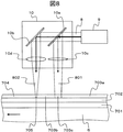
図7乃至図9は、実施例1のTFT基板の製造工程のうちのアモルファスシリコンを多結晶シリコン化する工程を説明するための模式図である。
図7は、実施例1の製造方法における連続発振レーザの照射方法を説明するための模式斜視図である。図8は、図7の連続発振レーザが照射されている領域をx方向と平行な面でみた模式断面図である。図9は、照射する連続発振レーザのエネルギー分布とエネルギー密度の関係を示す模式グラフ図である。なお、図9のエネルギー分布は、連続発振レーザの走査方向(移動方向)と平行な面でみた分布である。
7 to 9 are schematic views for explaining a process of converting amorphous silicon into polycrystalline silicon in the manufacturing process of the TFT substrate according to the first embodiment.
FIG. 7 is a schematic perspective view for explaining a continuous wave laser irradiation method in the manufacturing method of the first embodiment. FIG. 8 is a schematic cross-sectional view of a region irradiated with the continuous wave laser shown in FIG. 7 as viewed in a plane parallel to the x direction. FIG. 9 is a schematic graph showing the relationship between the energy distribution and energy density of the continuous wave laser to be irradiated. Note that the energy distribution in FIG. 9 is a distribution seen in a plane parallel to the scanning direction (movement direction) of the continuous wave laser.
水素化したアモルファスシリコン膜703aのうち、第1の駆動回路を形成する領域R1および第2の駆動回路を形成する領域R2を多結晶シリコン化するときには、たとえば、図7に示すように、それぞれ、マザーガラス6をx方向およびy方向に移動させながら走査して、各駆動回路を形成する各領域R1,R2およびその周辺領域に脱水素化する第1の連続発振レーザ801を照射し、続けて脱水素化されたアモルファスシリコン703bを溶融させる第2の連続発振レーザ802を照射する。なお、走査するときには、マザーガラス6を移動させてもよいし、連続発振レーザ801,802を照射する光学系を移動させてもよい。また、マザーガラス6および前記光学系の両方を移動させてもよい。
When the region R1 for forming the first drive circuit and the region R2 for forming the second drive circuit in the hydrogenated
第1の連続発振レーザ801および第2の連続発振レーザ802は、たとえば、1つのレーザ発振器9で発生させた1本の連続発振レーザ8を、光学系10で2本のビーム(連続発振レーザ)801,802にして照射する。光学系10には、たとえば、ハーフミラー10a、全反射ミラー10b、第1のレンズ10c、第2のレンズ10dを設けておく。そして、レーザ発振器9で発生させた連続発振レーザ8のうち、ハーフミラー10aで反射した方のビームを第1の連続発振レーザ801とし、第1のレンズ10cで焦点を調整してアモルファスシリコン膜703aに照射する。このとき、第1の連続発振レーザ801が照射されている領域のアモルファスシリコン膜703cは、照射により発生した熱により水素が蒸発し、含有量が徐々に減っていく。
In the first
また、レーザ発振器9で発生させた連続発振レーザ8のうち、ハーフミラー10aを透過した方のビームは第2の連続発振レーザ802とし、全反射ミラー10bで光路を変えた後、第2のレンズ10dで焦点を調整して脱水素化されたアモルファスシリコン703bに照射する。このとき、第2の連続発振レーザ802が照射されている領域のシリコン705は、溶融した状態であり、マザーガラス6(第2の連続発振レーザ802)が移動すると、結晶化して多結晶シリコン704になる。
Of the
なお、図8では省略しているが、光学系10には、たとえば、第1の連続発振レーザ801および第2の連続発振レーザ802の照射、遮断(非照射)の制御を行うためのシャッターまたは変調器などが設けられている。そして、たとえば、マザーガラス6を移動させながら走査するときに、マザーガラス6と光学系10の位置関係に基づいてシャッターの開閉を行えば、1度の走査で、x方向に並んだ複数の領域R1のアモルファスシリコン703aを多結晶シリコン化することができる。
Although omitted in FIG. 8, the
ところで、第1の連続発振レーザ801は、アモルファスシリコン703aを脱水素化するために照射するビームである。そのため、脱水素化されたアモルファスシリコン703bを溶融させる第2の連続発振レーザ802よりも弱いパワーで照射する必要がある。また、脱水素化したアモルファスシリコン703bに含まれる水素の量を限りなく0(零)に近づけるためには、可能な限り長い時間照射する必要がある。そのため、光学系10において第1の連続発振レーザ801および第2の連続発振レーザ802を形成するときには、それぞれの連続発振レーザ801,802のエネルギー分布とエネルギー密度の関係が、たとえば、図9に示すような関係になるようにする。図9のグラフにおいて、横軸は各連続発振レーザ801,802のエネルギー分布Edistであり、縦軸は各連続発振レーザ801,802のエネルギー密度Edenである。
By the way, the first
つまり、脱水素化に用いる第1の連続発振レーザ801は、エネルギー密度Edenを第2の連続発振レーザ802のエネルギー密度よりも小さくし、走査方向(移動方向)のエネルギー分布Edist(ビーム幅BW1)を第2の連続発振レーザ802のエネルギー分布(ビーム幅BW2)よりも広くする。ここで、ビーム幅BM1,BM2は、各連続発振レーザを走査方向に測った寸法である。このようなエネルギー分布Edistやエネルギー密度Edenが異なる2本の連続発振レーザ801,802を形成するには、たとえば、光学系10のハーフミラー10aの透過率および反射率、第1のレンズ10cおよび第2のレンズ10dの屈折率や焦点などを調整すればよい。
In other words, the first
図10は、実施例1のTFT基板の製造方法の作用効果を説明するための模式図である。 FIG. 10 is a schematic diagram for explaining the operational effects of the manufacturing method of the TFT substrate of Example 1.
実施例1の製造方法では、たとえば、図10に示すように、第1の連続発振レーザ801を照射して脱水素化されたアモルファスシリコン703bに第2の連続発振レーザ802を照射して溶融させる。第1の連続発振レーザ801および第2の連続発振レーザ802は、たとえば、マザーガラス6を−x方向に移動させながら照射するので、第2の連続発振レーザ802が照射されて溶融した領域は+x方向に移動していく。このとき、溶融したシリコン705は、第2の連続発振レーザ802が移動して照射されなくなると温度が低下して結晶化する。またこのとき、溶融したシリコン705は、第2の発振レーザ802の照射を開始した位置で溶融したシリコンが結晶化する際に形成された核が成長するように結晶化する。そのため、第2の連続発振レーザ802が照射された領域には、図10に示すように、概ね第2の連続発振レーザ802の移動方向(x方向)に沿って長く延びる帯状結晶(擬似単結晶)が多数形成される。
In the manufacturing method of the first embodiment, for example, as shown in FIG. 10, the
このとき、アモルファスシリコンを脱水素化する第1の連続発振レーザ801を照射する領域R3の面積を、第2の連続発振レーザを照射する領域R1の面積よりも広くしておくと、たとえば、図10に示すように、第2の連続発振レーザ802が照射されて溶融している領域と、水素化したアモルファスシリコン703aのままである領域の間に、脱水素化されたアモルファスシリコン703bの領域が介在している。そのため、照射された第2の連続発振レーザ802の熱により水素化したアモルファスシリコン703aが突沸することを防げ、多結晶シリコン化された領域R1の外周部における多結晶シリコン704の質の低下を防ぐことができる。このとき、第1の連続発振レーザ801の長軸方向の寸法は、第2の連続発振レーザ802の長軸方向の寸法よりも大きいことが望ましい。
At this time, if the area of the region R3 irradiated with the first
このように、マザーガラス6を−x方向に移動させながら第1の駆動回路を形成する各領域R1に第1の連続発振レーザ801および第2の連続発振レーザ802を照射すれば、第1の駆動回路を形成する各領域R1には、図7に矢印で示した方向(x方向)に長く延びた帯状結晶の集合でなる多結晶シリコン704が形成される。そのため、第1の駆動回路を形成する領域R1にTFT素子を形成するときに、たとえば、チャネル長の方向(キャリアの移動方向)がx方向になるようにソース電極およびドレイン電極を形成すれば、キャリアの移動度が高くなり、TFT素子の動作を高速化できる。
In this way, if the first
また、詳細な説明は省略するが、たとえば、第2の駆動回路を形成する各領域R2を多結晶シリコン化するときには、たとえば、図7に示したy方向がx方向になるようにマザーガラス6を90度回転させて、マザーガラス6を−y方向に移動させながら第2の駆動回路を形成する各領域R2に第1の連続発振レーザ801および第2の連続発振レーザ802を照射すればよい。こうすると、第2の駆動回路を形成する各領域R2には、図7に矢印で示した方向(y方向)に長く延びた帯状結晶の集合でなる多結晶シリコン704が形成される。そのため、たとえば、第2の駆動回路を形成する領域R2にTFT素子を形成するときに、チャネル長の方向がy方向になるようにソース電極およびドレイン電極を形成すれば、キャリアの移動度が高くなり、TFT素子の動作を高速化できる。
Although detailed description is omitted, for example, when each region R2 forming the second drive circuit is made into polycrystalline silicon, for example, the
なお、実施例1では、TFT基板1の製造工程のうち、表示領域DAの各画素のTFT素子の半導体層として用いるアモルファスシリコン膜703aと、第1の駆動回路DRV1および第2の駆動回路DRV2の半導体素子の半導体層として用いる多結晶シリコン膜704とを形成する工程のみについて説明している。このとき、TFT基板1の製造工程におけるその他の工程、たとえば、走査信号線GLを形成する工程、映像信号線DLを形成する工程、画素電極PXを形成する工程などは、従来のTFT基板1を製造するときと同じ手順で行えばよい。またこのとき、各工程の順序や、表示領域DAのTFT素子の構成、第1の駆動回路DRV1および第2の駆動回路DRV2の半導体素子の構成は任意であり、従来のTFT基板で適用されている順序、構成の中から適宜選択すればよい。
In the first embodiment, in the manufacturing process of the
また、実施例1の製造方法を適用して製造されるTFT基板1は、表示領域DAの各画素のTFT素子の半導体層がアモルファスシリコン703aである。そのため、表示領域DAのTFT素子は、ガラス基板(マザーガラス6)と半導体層(アモルファスシリコン703a)の間にゲート電極が配置されたTFT素子(ボトムゲート型のTFT素子)にすることが望ましい。しかしながら、表示領域DAのTFT素子は、これに限らず、ガラス基板(マザーガラス6)から見て半導体層(アモルファスシリコン703a)よりも上の層にゲート電極が配置されたTFT素子(トップゲート型のTFT素子)でもよいことはもちろんである。
Further, in the
また、表示領域DAのTFT素子をボトムゲート型のTFT素子にした場合、たとえば、第1の駆動回路DRV1および第2の駆動回路DRV2のTFT素子もボトムゲート型のTFT素子にすれば、表示領域DAのTFT素子のゲート電極と第1の駆動回路DRV1および第2の駆動回路DRV2のTFT素子を1つの工程で形成することができる。 When the TFT element in the display area DA is a bottom gate type TFT element, for example, if the TFT elements of the first drive circuit DRV1 and the second drive circuit DRV2 are also bottom gate type TFT elements, the display area The gate electrode of the TFT element of DA and the TFT elements of the first drive circuit DRV1 and the second drive circuit DRV2 can be formed in one step.
しかしながら、第1の駆動回路DRV1および第2の駆動回路DRV2のTFT素子をボトムゲート型にする場合、半導体層となる多結晶シリコンを形成するときに、アモルファスシリコン膜703aの下にゲート電極があるため、アモルファスシリコン膜703aに凹凸が生じ、たとえば、熱伝導率の不均一に伴う結晶化の面内ばらつきが生じることがある。そのため、第1の駆動回路DRV1および第2の駆動回路DRV2のTFT素子をトップゲート型のTFT素子にすれば、結晶化の面内ばらつきが生じにくくなり、各TFT素子の特性のばらつきを生じにくくすることができる。
However, when the TFT elements of the first drive circuit DRV1 and the second drive circuit DRV2 are of bottom gate type, a gate electrode is provided under the
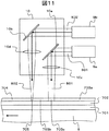
図11は、実施例1の製造方法における連続発振レーザの形成方法の変形例を説明するための模式図である。 FIG. 11 is a schematic diagram for explaining a modification of the continuous wave laser forming method in the manufacturing method of the first embodiment.
実施例1のTFT基板1の製造方法において、第1の連続発振レーザ801および第2の連続発振レーザ802を形成する光学系10を、たとえば、図8のような構成にすると、1つのレーザ発振器9から2つの連続発振レーザ801,802を形成することができる。しかしながら、実施例1の製造方法では、これに限らず、たとえば、図11に示すように、2つのレーザ発振器9a,9bを用い、第1の発振器9aでアモルファスシリコンを脱水素化する第1の連続発振レーザ801を発生させ、第2の発振器9bで脱水素化したアモルファスシリコンを溶融させる第2の連続発振レーザ802を発生させてもよい。この場合、第1の連続発振レーザ801は、たとえば、第1の全反射ミラー10eで光路を変え、第1のレンズ10cを通してアモルファスシリコン膜703aに照射する。また、第2の連続発振レーザ802は、たとえば、第2の全反射ミラー10bで光路を変え、第2のレンズ10dを通して脱水素化されたアモルファスシリコン703bに照射する。またこのとき、第1の連続発振レーザ801および第2の連続発振レーザ802の移動方向のビーム幅は、たとえば、第1のレンズ10cおよび第2のレンズ10dの屈折率や焦点を調整すればよい。
In the manufacturing method of the
図12は、実施例1のTFT基板の製造方法における多結晶シリコンの形成方法の第1の変形例を説明するための模式図である。図13は、実施例1のTFT基板の製造方法における多結晶シリコンの形成方法の第2の変形例を説明するための模式図である。図14は、実施例1のTFT基板1の製造方法における多結晶シリコンの形成方法の第3の変形例を説明するための模式図である。
FIG. 12 is a schematic diagram for explaining a first modification of the method for forming polycrystalline silicon in the method for manufacturing a TFT substrate according to the first embodiment. FIG. 13 is a schematic diagram for explaining a second modification of the method for forming polycrystalline silicon in the method for manufacturing the TFT substrate of Example 1. FIG. FIG. 14 is a schematic diagram for explaining a third modification of the method for forming polycrystalline silicon in the method for manufacturing the
アモルファスシリコン膜703aを脱水素化し、多結晶シリコン化する手順として、図7および図8に示した例は、マザーガラス6の上の、ある帯状領域を一方向(+x方向)に走査する場合のみを示している。このとき、前記ある帯状領域を一度走査するだけで、すべての第1の駆動回路を形成する領域R1を多結晶シリコン化できる場合もあるが、中には、2つの第1の駆動回路を形成する領域R1,R1’がy方向に並んでいるような場合もある。その場合、たとえば、図12の上側に示すように、一方の駆動回路を形成する領域R1が含まれる帯状領域を+x方向に走査しながら第1の連続発振レーザ801および第2の連続発振レーザ802を照射して多結晶シリコン704を形成した後、マザーガラス6をy方向に移動させて、図12の下側に示すように、他方の駆動回路を形成する領域R1’が含まれる帯状領域を−x方向に走査しながら第1の連続発振レーザ801および第2の連続発振レーザ802を照射して多結晶シリコン704を形成すると、各領域R1,R1’に効率よく多結晶シリコン704を形成することができる。
As a procedure for dehydrogenating the
なお、図12に示したような走査方法に限らず、たとえば、図13に示すように、一方の駆動回路を形成する領域R1が含まれる帯状領域を+x方向に走査しながら第1の連続発振レーザ801および第2の連続発振レーザ802を照射して多結晶シリコン704を形成した後、マザーガラス6と光学系の位置関係を走査前の関係に戻し、マザーガラス6をy方向に移動させ、他方の駆動回路を形成する領域R1’が含まれる帯状領域を再び+x方向に走査しながら第1の連続発振レーザ801および第2の連続発振レーザ802を照射して多結晶シリコン704を形成してもよいことはもちろんである。
In addition to the scanning method shown in FIG. 12, for example, as shown in FIG. 13, the first continuous oscillation is performed while scanning the band-like region including the region R1 forming one drive circuit in the + x direction. After irradiating the
またさらに、実施例1では、第1の連続発振レーザ801および第2の連続発振レーザ802を同一方向に移動させ、脱水素化されたアモルファスシリコン703bを順次溶融、多結晶シリコン704を形成しているが、これに限らず、たとえば、図14の上側に示すように+x方向に走査するときには第1の連続発振レーザ801の照射のみを行って脱水素化されたアモルファスシリコン703bを形成し、その後、y方向の位置を固定したまま折り返し、図14の下側に示すように−x方向に走査するときには第2の連続発振レーザ802の照射のみを行って脱水素化されたアモルファスシリコン703bを溶融させ、多結晶シリコン704を形成してもよい。また、図示は省略するが、図14の上側に示すように+x方向に走査して脱水素化されたアモルファスシリコン703bを形成した後、たとえば、マザーガラス6を走査前の位置に戻し、再び+x方向に走査して多結晶シリコン704を形成してもよいことはもちろんである。
Furthermore, in Example 1, the first
このように、1回目の走査で脱水素化を行い、2回目の走査で多結晶シリコン化する場合、たとえば、脱水素化の際の第1の連続発振レーザ801の移動速度(走査速度)と、多結晶シリコン化の際の第2の連続発振レーザ802の移動速度(走査速度)を独立して設定することができる。そのため、たとえば、脱水素化をするときの速度Vprを、多結晶シリコン化するときの速度Vrcより小さくすれば、脱水素化の際に、脱水素化する領域R3の各点に、第1の連続発振レーザ801が照射されている時間を長くすることができ、脱水素化したアモルファスシリコン703bに残存する水素の量を限りなく零に近づけることができる。
Thus, when dehydrogenation is performed in the first scan and polycrystalline silicon is formed in the second scan, for example, the moving speed (scanning speed) of the first
また、実施例1では、アモルファスシリコン703aの脱水素化と、脱水素化されたアモルファスシリコン703bの多結晶シリコン化を、1つの工程としてとらえ、脱水素化されたアモルファスシリコン703bを順次多結晶シリコン化していく方法について説明している。しかしながら、実施例1の製造方法は、これに限らず、たとえば、脱水素化する工程と、多結晶シリコン化する工程の2つの工程にわけてもよいことはもちろんである。このとき、アモルファスシリコン703aを脱水素化する工程は、たとえば、酸素雰囲気中で行うことが望ましい。
Further, in Example 1, the dehydrogenation of the
図15および図16は、本発明による実施例2のTFT基板の製造方法を説明するための模式図である。
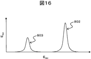
図15は、実施例2の製造方法における連続発振レーザの照射方法を説明するための模式断面図である。図16は、照射する連続発振レーザのエネルギー分布とエネルギー密度の関係を示す模式グラフ図である。なお、図16は、脱水素化されたアモルファスシリコンを溶融させる第2の連続発振レーザと、多結晶シリコン化された領域に照射する第3の連続発振レーザのエネルギー分布とエネルギー密度の関係を示しており、横軸がエネルギー分布Edistであり、縦軸がエネルギー密度Edenである。また、図16のエネルギー分布Edistは、連続発振レーザの走査方向(移動方向)と平行な面でみた分布である。
15 and 16 are schematic views for explaining a manufacturing method of the TFT substrate of Example 2 according to the present invention.
FIG. 15 is a schematic cross-sectional view for explaining a continuous wave laser irradiation method in the manufacturing method of the second embodiment. FIG. 16 is a schematic graph showing the relationship between energy distribution and energy density of the continuous wave laser to be irradiated. FIG. 16 shows the relationship between the energy distribution and the energy density of the second continuous wave laser that melts the dehydrogenated amorphous silicon and the third continuous wave laser that irradiates the polycrystalline siliconized region. The horizontal axis is the energy distribution E dist and the vertical axis is the energy density E den . Also, the energy distribution E dist in FIG. 16 is a distribution viewed on a plane parallel to the scanning direction (movement direction) of the continuous wave laser.
実施例2では、前記実施例1で説明したアモルファスシリコンを多結晶シリコン化する方法を前提にし、形成された多結晶シリコンを構成する各結晶の形状を安定にし、かつ、結晶粒界を少なくする方法について説明する。 In Example 2, on the premise of the method for converting amorphous silicon into polycrystalline silicon described in Example 1, the shape of each crystal constituting the formed polycrystalline silicon is stabilized and the number of crystal grain boundaries is reduced. A method will be described.
アモルファスシリコンを多結晶シリコン化するときには、たとえば、前記実施例1で説明したように、アモルファスシリコン703aに第1の連続発振レーザ801を照射して脱水素化した後、脱水素化されたアモルファスシリコン703bに第2の連続発振レーザ802を照射して一度溶融させ、その溶融したシリコン705が冷却する過程で多結晶シリコン化させる。しかしながら、前記実施例1のような方法で多結晶シリコン化させる場合、たとえば、結晶化の際の温度変化(低下)が急激であるため、多結晶シリコンを構成する各結晶の形状のばらつきが大きくなる、各結晶のサイズが小さくて結晶粒界が多くなるといったことが生じやすい。そのため、多結晶シリコンを半導体層とするTFT素子を形成したときに、各TFT素子の特性にばらつきが生じることがある。
When the amorphous silicon is converted into polycrystalline silicon, for example, as described in the first embodiment, the
このような多結晶シリコンを構成する各結晶の形状のばらつきを低減するとともに、結晶粒界を少なくするには、たとえば、図15に示すように、第2の連続発振レーザ802を照射して溶融したシリコン705が結晶化した多結晶シリコン704aに、第3の連続発振レーザ803を照射してポストアニールすればよいことを、本願発明者らは見出した。
In order to reduce the variation in the shape of each crystal constituting such polycrystalline silicon and reduce the crystal grain boundary, for example, as shown in FIG. 15, the second
このとき、アモルファスシリコン703aを脱水素化する第1の連続発振レーザ801、脱水素化されたアモルファスシリコン703bを溶融させる第2の連続発振レーザ802、溶融したシリコン705が結晶化するときの多結晶シリコン704aの急激な温度低下を緩和する第3の連続発振レーザ803は、たとえば、図15に示したように、1つのレーザ発振器9で発生させた連続発振レーザ8を光学系10で3つの連続発振レーザ(ビーム)にして照射すればよい。このとき、図示は省略するが、光学系10には、たとえば、2つのハーフミラーを設けて1本の連続発振レーザ8を3つにわけ、レンズの屈折率や焦点を調節して各連続発振レーザ801,802,803の走査方向(移動方向)の幅を調整し、マザーガラス6に照射すればよい。
At this time, a first
またこのとき、第3の連続発振レーザ803は、溶融したシリコン705が結晶化するときの多結晶シリコン704aの急激な温度低下を緩和するために照射するレーザである。そのため、第3の連続発振レーザ803のエネルギー密度Eden(パワー)は、たとえば、図16に示すように、第2の連続発振レーザ802のエネルギー密度よりも低くする。また、図16では省略しているが、第1の連続発振レーザ801と第2の連続発振レーザ802のエネルギー分布Edistとエネルギー密度Edenの関係は、図9に示したような関係にする。
At this time, the third
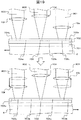
図17は、実施例2の連続発振レーザの照射方法の作用効果を説明するための模式図である。なお、図17に示した2つの図のうち、上側に示した図は実施例1の方法で溶融させたシリコン305を多結晶化した場合の結晶の様子を示す模式平面図であり、下側の図は、実施例2の方法で第3の連続発振レーザ803を照射しながら多結晶化した場合の結晶の状態を示す模式平面図である。また、図17に示した2つの図は、マザーガラス6上の同じ領域を同じ寸法で示している。
FIG. 17 is a schematic diagram for explaining the operational effects of the continuous wave laser irradiation method according to the second embodiment. Of the two diagrams shown in FIG. 17, the diagram shown on the upper side is a schematic plan view showing the state of the crystal when the silicon 305 melted by the method of Example 1 is polycrystallized. FIG. 6 is a schematic plan view showing a crystal state when polycrystallized while irradiating the third
実施例1で説明した製造方法のように、第2の連続発振レーザ802を照射した後、溶融したシリコン705をそのまま多結晶化させる場合、第2の連続発振レーザ802の照射領域から外れた後、溶融したシリコン705は急激に温度が低下する。そのため、凝固点に達したときに、たとえば、多くの核が生成されて、図17の上側に示すように、走査方向の長さが比較的短い帯状結晶704pが多数形成される。そのため、結晶粒界が多くなり、TFT素子の半導体層を形成したときに、キャリアの移動度が低くなることがある。
When the melted
一方、実施例2のように、第2の連続発振レーザ802の照射領域から外れた後、溶融したシリコン705が多結晶化している領域に第3の連続発振レーザ803を照射すると、溶融したシリコン705の温度変化(低下)が緩やかになるので、たとえば、生成される核の数が少なくなり、すでに結晶化した帯状結晶704pが成長するような結晶化が進む。そのため、図17の下側に示すように、走査方向の長さが、第3の連続発振レーザ803を照射しない場合よりも長い帯状結晶704pが形成される。そのため、結晶粒界が少なくなり、TFT素子の半導体層を形成したときに、キャリアの移動度が低くなるのを防げる。
On the other hand, when the third
このように、第3の連続発振レーザ803を照射しながら、溶融したシリコン705を多結晶化することで、多結晶シリコンの結晶粒界を少なくでき、第1の駆動回路DRV1や第2の駆動回路DRV2の各TFT素子の特性のばらつきを低減することができる。
In this way, by crystallizing the melted
なお、実施例2でも、TFT基板1の製造工程のうち、表示領域DAの各画素のTFT素子の半導体層として用いるアモルファスシリコン膜703aと、第1の駆動回路DRV1および第2の駆動回路DRV2の半導体素子の半導体層として用いる多結晶シリコン膜704とを形成する工程のみについて説明している。それ以外の部分は、実施例1と同様なので説明を省略する。
Also in the second embodiment, in the manufacturing process of the
図18は、実施例2のTFT基板の製造方法における多結晶シリコンの形成方法の変形例を説明するための模式図である。図19は、図18に示した多結晶シリコンの形成方法における連続発振レーザの照射方法の一例を説明するための模式図である。 FIG. 18 is a schematic diagram for explaining a modification of the method for forming polycrystalline silicon in the method for manufacturing a TFT substrate according to the second embodiment. FIG. 19 is a schematic diagram for explaining an example of a continuous wave laser irradiation method in the polycrystalline silicon forming method shown in FIG.
実施例2の製造方法において、たとえば、第1の駆動回路を形成する領域R1が複数箇所にあるときに、マザーガラス6の上の、ある帯状領域を一度走査するだけで、すべての第1の駆動回路を形成する領域R1を多結晶シリコン化できる場合もあるが、中には、2つの第1の駆動回路を形成する領域R1,R1’がy方向に並んでいるような場合もある。その場合、たとえば、図18の上側に示すように、一方の駆動回路を形成する領域R1が含まれる帯状領域を+x方向に走査しながら第1の連続発振レーザ801および第2の連続発振レーザ802ならびに第3の連続発振レーザ803を照射して結晶粒界が少ない多結晶シリコン704bを形成した後、マザーガラス6をy方向に移動させて、図18の下側に示すように、他方の駆動回路を形成する領域R1’が含まれる帯状領域を−x方向に走査しながら第1の連続発振レーザ801および第2の連続発振レーザ802ならびに第3の連続発振レーザ803を照射して多結晶シリコン704bを形成すると、各領域R1,R1’に効率よく多結晶シリコン704bを形成することができる。
In the manufacturing method of the second embodiment, for example, when there are a plurality of regions R1 that form the first drive circuit, all the first regions can be obtained by scanning a certain strip region on the
このとき、一方の駆動回路を形成する領域R1が含まれる帯状領域を+x方向に走査して多結晶シリコン704bを形成した後、たとえば、光学系10を180度回転させて、第1の連続発振レーザ801、第2の連続発振レーザ802、第3の連続発振レーザ803の並び順を反転してから、他方の駆動回路を形成する領域R1’が含まれる帯状領域を−x方向に走査して多結晶シリコン704bを形成することも可能であるが、光学系10を反転させるときに、角度や各連続発振レーザのy方向の照射位置がずれてしまう可能性がある。
At this time, after forming the
そのため、図18に示したような走査方法で駆動回路を形成する領域R1,R1’に多結晶シリコン704bを形成するときには、たとえば、第1の連続発振レーザ801のエネルギー分布およびエネルギー密度と、第3の連続発振レーザ803のエネルギー分布およびエネルギー密度を、走査方向(移動方向)に応じて変化させることが望ましい。つまり、一方の駆動回路を形成する領域R1が含まれる帯状領域を+x方向に走査して多結晶シリコン704bを形成するときには、たとえば、図19の上側に示すように、第1のレンズ10c、第2のレンズ10d、第3のレンズ10fの位置を変えて焦点やビーム幅を調整し、第1の連続発振レーザ801はアモルファスシリコン703aの脱水素化に適したビーム、第2の連続発振レーザ802で脱水素化されたアモルファスシリコン703bを溶融させるのに適したビーム、第3の連続発振レーザ803は多結晶シリコン704aをポストアニールするのに適したビームにして照射する。そして、他方の駆動回路を形成する領域R1’が含まれる帯状領域を−x方向に走査して多結晶シリコン704bを形成するときには、たとえば、図19の下側に示すように、第1のレンズ10cと第3のレンズ10fの位置を変えて焦点やビーム幅を調整し、第1の連続発振レーザ801は多結晶シリコン704aをポストアニールするのに適したビーム、第2の連続発振レーザ802で脱水素化されたアモルファスシリコン703bを溶融させるのに適したビーム、第3の連続発振レーザ803はアモルファスシリコン703aの脱水素化に適したビームにして照射する。
Therefore, when the
このように、走査方向によって第1の連続発振レーザ801の役割と第3の連続発振レーザ803の役割を入れ替えることで、たとえば、光学系10を反転させることなく、各領域R1,R1’に多結晶シリコン704bを形成することができる。そのため、角度や各連続発振レーザのy方向の照射位置のずれを防ぐことができる。
In this way, by changing the role of the first
また、実施例2の製造方法において、第1の連続発振レーザ801、第2の連続発振レーザ802、第3の連続発振レーザ803は、たとえば、それぞれ独立したレーザ発振器および光学系の組み合わせによって生成し、照射してもよいことはもちろんである。
In the manufacturing method of the second embodiment, the first
また、実施例2の製造方法では、脱水素化されたアモルファスシリコン703bの多結晶シリコン化と、第3の連続発振レーザ803によるポストアニールを、1つの工程としてとらえ、溶融したシリコン705が多結晶シリコン化して過程でポストアニールを行う方法について説明している。しかしながら、実施例2の製造方法は、これに限らず、たとえば、第1の連続発振レーザ801を照射してアモルファスシリコンを脱水素化する工程と、脱水素化されたアモルファスシリコンに第2の連続発振レーザ802および第3の連続発振レーザ803を照射して多結晶シリコン化する工程を分けてもよいことはもちろんである。また、第3の連続発振レーザ803の照射位置は、基本的には、第2の連続発振レーザ802の照射位置に近いほうが望ましく、第2の連続発振レーザ802の移動速度(走査速度)と第3の連続発振レーザ803の移動速度(走査速度)とは同じ速度にすることが望ましい。しかしながら、これに限らず、第2の連続発振レーザ802の移動速度と第3の連続発振レーザ803の移動速度とが異なる速度であってもよいことはもちろんである。
Further, in the manufacturing method of Example 2, the dehydrogenated
また、アモルファスシリコンの脱水素化と多結晶シリコン化を分けて行う場合、たとえば、脱水素化は酸素雰囲気中で行い、多結晶シリコン化は、たとえば、不活性ガス雰囲気中で行うことが望ましい。 Further, when dehydrogenation of amorphous silicon and polycrystalline silicon are performed separately, for example, dehydrogenation is preferably performed in an oxygen atmosphere, and polycrystalline silicon is desirably performed in, for example, an inert gas atmosphere.
以上、本発明を、前記実施例に基づき具体的に説明したが、本発明は、前記実施例に限定されるものではなく、その要旨を逸脱しない範囲において、種々変更可能であることはもちろんである。 The present invention has been specifically described above based on the above-described embodiments. However, the present invention is not limited to the above-described embodiments, and various modifications can be made without departing from the scope of the present invention. is there.
たとえば、実施例1および実施例2では、第2の連続発振レーザを照射することにより一方向に長く延びる帯状結晶(擬似単結晶)704pに改質する場合を示しているが、これに限られず、第2の連続発振レーザを照射することにより粒状結晶または微結晶で構成された多結晶シリコンに改質してもよい。さらにその後、粒状結晶または微結晶に連続発振レーザを照射して、擬似単結晶に改質しても良い。なお、多結晶シリコンを構成する各結晶の形状や大きさは、連続発振レーザのエネルギー密度や走査速度を変えることで変化させることができる。これにより、帯状結晶704pに限らず、粒径が0.3μm以下の微結晶の集合でなる多結晶シリコンや、粒径が0.3μmから1μm程度の粒状結晶の集合でなる多結晶シリコンを形成することもできる。
For example, in the first and second embodiments, the case where the second continuous wave laser is irradiated to be modified into a band-like crystal (pseudo single crystal) 704p extending in one direction is shown, but the present invention is not limited to this. Alternatively, it may be modified to polycrystalline silicon composed of granular crystals or microcrystals by irradiation with a second continuous wave laser. Thereafter, the granular crystal or the microcrystal may be irradiated with a continuous wave laser to be modified into a pseudo single crystal. Note that the shape and size of each crystal constituting the polycrystalline silicon can be changed by changing the energy density and scanning speed of the continuous wave laser. Thus, not only the band-
また、実施例1および実施例2では、アクティブマトリクス型の液晶表示パネルに用いられるTFT基板1を例に挙げ、その製造方法を説明しているが、本発明は、これに限らず、図2および図3に示したTFT基板1と同等の構成を有する基板(表示パネル)の製造方法に適用できることはもちろんである。すなわち、本発明の表示装置の製造方法は、たとえば、表示領域の外側に駆動回路などの集積回路を有し、表示領域のTFT素子の半導体層をアモルファスシリコンで形成し、集積回路の半導体素子の半導体層を多結晶シリコンで形成する基板(表示パネル)であれば、どのようなものにも適用することができる。アクティブマトリクス型の液晶表示パネルのTFT基板1の他に、本発明の製造方法が適用可能なものとしては、たとえば、有機EL(ElectroLuminescence)を用いた自発光型の表示パネルなどがある。
In the first and second embodiments, the
また、実施例1および実施例2では、アモルファスシリコンを多結晶シリコン化する場合を例に挙げたが、これに限らず、他の半導体材料を用いてもよいことはもちろんである。 In the first and second embodiments, the case where amorphous silicon is converted to polycrystalline silicon is described as an example. However, the present invention is not limited to this, and other semiconductor materials may be used.
1…TFT基板
2…対向基板
3…液晶材料
4…シール材
5a,5b…偏光板
6…マザーガラス
701…シリコン窒化膜(SiN膜)
702…シリコン酸化膜(SiO膜)
703a…水素化したアモルファスシリコン(膜)
703b…脱水素化されたアモルファスシリコン(膜)
704,704a,704b…多結晶シリコン
704p…帯状結晶
704w…帯状結晶(擬似単結晶)
705…溶融したシリコン
801…第1の連続発振レーザ
802…第2の連続発振レーザ
803…第3の連続発振レーザ
9…レーザ発振器
9a…第1のレーザ発振器
9b…第2のレーザ発振器
10…光学系
10a…ハーフミラー
10b…全反射ミラー(第2の全反射ミラー)
10c…第1のレンズ
10d…第2のレンズ
10e…第1の全反射ミラー
10f…第3のレンズ
GL,GLm,GLm+1…走査信号線
DL,DLn,GLn+1…走査信号線
PX…画素電極
CT…共通電極
DA…表示領域
DRV1…第1の駆動回路
DRV2…第2の駆動回路
DESCRIPTION OF
702 ... Silicon oxide film (SiO film)
703a ... Hydrogenated amorphous silicon (film)
703b ... dehydrogenated amorphous silicon (film)
704, 704a, 704b ...
705 ...
10c ... the
Claims (16)
前記水素化したアモルファスシリコン膜のあらかじめ定められた領域を脱水素化した後、前記脱水素化された領域のアモルファスシリコンを溶融、結晶化して多結晶シリコンにする第2の工程とを有し、
前記基板の表示領域にアモルファスシリコンを用いたTFT素子を有する複数の画素を形成するとともに、該表示領域の外側に、多結晶シリコンを用いた複数個の半導体素子を有する駆動回路を形成する表示装置の製造方法であって、
前記第2の工程は、前記基板の前記表示領域の外側にある前記駆動回路を形成する領域およびその周辺領域のみを第1の連続発振レーザを照射して脱水素化した後、前記脱水素化された領域のみに第2の連続発振レーザを照射して前記アモルファスシリコンを前記多結晶シリコンにし、
前記第1の連続発振レーザを照射する領域は、前記第2の連続発振レーザを照射する領域よりも広いことを特徴とする表示装置の製造方法。 A first step of forming a hydrogenated amorphous silicon film on a substrate;
A second step of dehydrogenating a predetermined region of the hydrogenated amorphous silicon film, and then melting and crystallizing amorphous silicon in the dehydrogenated region into polycrystalline silicon,
A display device in which a plurality of pixels having TFT elements using amorphous silicon are formed in a display region of the substrate, and a driving circuit having a plurality of semiconductor elements using polycrystalline silicon is formed outside the display region A manufacturing method of
In the second step, the region where the drive circuit is formed outside the display region of the substrate and the peripheral region thereof are dehydrogenated by irradiating the first continuous wave laser, and then the dehydrogenation is performed. Irradiating a second continuous wave laser only to the formed region to change the amorphous silicon into the polycrystalline silicon,
A method for manufacturing a display device, wherein a region irradiated with the first continuous wave laser is wider than a region irradiated with the second continuous wave laser.
前記第1の連続発振レーザのエネルギー密度は、前記第2の連続発振レーザのエネルギー密度よりも低く、
前記第1の連続発振レーザおよび前記第2の連続発振レーザが照射する領域の各点は、前記第1の連続発振レーザが照射されている時間が、前記第2の連続発振レーザが照射されている時間よりも長いことを特徴とする請求項1に記載の表示装置の製造方法。 The first continuous wave laser and the second continuous wave laser are irradiated while scanning over the substrate,
The energy density of the first continuous wave laser is lower than the energy density of the second continuous wave laser,
Each point of the region irradiated with the first continuous wave laser and the second continuous wave laser is irradiated with the second continuous wave laser during the time when the first continuous wave laser is irradiated. The method for manufacturing a display device according to claim 1, wherein the time is longer than a predetermined time.
8. The method according to claim 1, wherein the second step irradiates the third continuous-wave laser to the polycrystalline siliconized region by irradiating the second continuous-wave laser. 9 . The manufacturing method of the display apparatus of any one .
前記別の帯状領域を走査するときは、前記第3の連続発振レーザを照射して前記水素化したアモルファスシリコン膜を脱水素化し、前記第3の連続発振レーザによって脱水素化されたアモルファスシリコンに前記第2の連続発振レーザを照射して多結晶シリコン化し、前記第2の連続発振レーザを照射して前記多結晶シリコン化された領域に前記第1の連続発振レーザを照射することを特徴とする請求項8または請求項9に記載の表示装置の製造方法。 In the second step, after scanning a certain band-shaped area on the substrate in the first direction, a band-shaped area different from the certain band-shaped area is scanned in a direction opposite to the first direction,
When scanning the other band-shaped region, the hydrogenated amorphous silicon film is dehydrogenated by irradiating the third continuous wave laser, and the amorphous silicon dehydrogenated by the third continuous wave laser is transformed into Irradiating the second continuous wave laser to form polycrystalline silicon, and irradiating the second continuous wave laser to irradiate the first continuous wave laser to the polycrystalline siliconized region. The manufacturing method of the display apparatus of Claim 8 or Claim 9 to do.
前記TFT基板を形成する工程は、前記基板の上に水素化したアモルファスシリコン膜を成膜する第1の工程と、The step of forming the TFT substrate includes a first step of forming a hydrogenated amorphous silicon film on the substrate,
前記水素化したアモルファスシリコン膜のあらかじめ定められた領域を脱水素化した後、前記脱水素化された領域のアモルファスシリコンを溶融、結晶化する第2の工程とを有し、A second step of melting and crystallizing amorphous silicon in the dehydrogenated region after dehydrogenating a predetermined region of the hydrogenated amorphous silicon film,
前記基板の表示領域にアモルファスシリコンを用いたTFT素子を有する複数の画素を形成するとともに、該表示領域の外側に前記第2の工程で結晶化されたシリコンを用いた複数のTFT素子を有する駆動回路を形成し、A plurality of pixels having TFT elements using amorphous silicon in the display area of the substrate and driving having a plurality of TFT elements using silicon crystallized in the second step outside the display area Forming a circuit,
前記第2の工程は、前記基板の前記表示領域の外側にある前記駆動回路を形成する領域およびその周辺領域のみを第1の連続発振レーザを照射して脱水素化した後、前記脱水素化された領域のみに第2の連続発振レーザを照射して前記アモルファスシリコンを溶融、結晶化し、In the second step, the region where the drive circuit is formed outside the display region of the substrate and the peripheral region thereof are dehydrogenated by irradiating the first continuous wave laser, and then the dehydrogenation is performed. Only the region is irradiated with a second continuous wave laser to melt and crystallize the amorphous silicon,
前記第1の連続発振レーザを照射する領域は、前記第2の連続発振レーザを照射する領域よりも広いことを特徴とする表示装置の製造方法。A method for manufacturing a display device, wherein a region irradiated with the first continuous wave laser is wider than a region irradiated with the second continuous wave laser.
前記第1の連続発振レーザのエネルギー密度は、前記第2の連続発振レーザのエネルギー密度よりも低く、The energy density of the first continuous wave laser is lower than the energy density of the second continuous wave laser,
前記第1の連続発振レーザおよび前記第2の連続発振レーザが照射する領域の各点は、前記第1の連続発振レーザが照射されている時間が、前記第2の連続発振レーザが照射されている時間よりも長いことを特徴とする請求項12に記載の表示装置の製造方法。Each point of the region irradiated with the first continuous wave laser and the second continuous wave laser is irradiated with the second continuous wave laser during the time when the first continuous wave laser is irradiated. The method of manufacturing a display device according to claim 12, wherein the time is longer than a certain time.
Priority Applications (2)
| Application Number | Priority Date | Filing Date | Title |
|---|---|---|---|
| JP2006227265A JP5085902B2 (en) | 2006-08-24 | 2006-08-24 | Manufacturing method of display device |
| US11/882,828 US7732268B2 (en) | 2006-08-24 | 2007-08-06 | Manufacturing method of display device |
Applications Claiming Priority (1)
| Application Number | Priority Date | Filing Date | Title |
|---|---|---|---|
| JP2006227265A JP5085902B2 (en) | 2006-08-24 | 2006-08-24 | Manufacturing method of display device |
Publications (3)
| Publication Number | Publication Date |
|---|---|
| JP2008053394A JP2008053394A (en) | 2008-03-06 |
| JP2008053394A5 JP2008053394A5 (en) | 2009-07-09 |
| JP5085902B2 true JP5085902B2 (en) | 2012-11-28 |
Family
ID=39197202
Family Applications (1)
| Application Number | Title | Priority Date | Filing Date |
|---|---|---|---|
| JP2006227265A Expired - Fee Related JP5085902B2 (en) | 2006-08-24 | 2006-08-24 | Manufacturing method of display device |
Country Status (2)
| Country | Link |
|---|---|
| US (1) | US7732268B2 (en) |
| JP (1) | JP5085902B2 (en) |
Families Citing this family (9)
| Publication number | Priority date | Publication date | Assignee | Title |
|---|---|---|---|---|
| JP5068972B2 (en) * | 2006-09-12 | 2012-11-07 | 富士フイルム株式会社 | Laser annealing apparatus, semiconductor film substrate, element substrate, and electro-optical device |
| EP2328169A1 (en) | 2008-09-18 | 2011-06-01 | Sharp Kabushiki Kaisha | Motherboard, motherboard manufacturing method and device board |
| JP2010108957A (en) * | 2008-10-28 | 2010-05-13 | Hitachi Displays Ltd | Display device and method of manufacturing the same |
| US9111803B2 (en) * | 2011-10-03 | 2015-08-18 | Joled Inc. | Thin-film device, thin-film device array, and method of manufacturing thin-film device |
| KR102014167B1 (en) * | 2012-12-06 | 2019-10-22 | 삼성디스플레이 주식회사 | Method for manufacturing poly-crystallation silicon layer, method for manufacturing orgainc light emitting display apparatus comprising the same, and organic light emitting display apparatus manufactured by the same |
| NL2013715B1 (en) * | 2014-10-30 | 2016-10-04 | Univ Delft Tech | Low-temperature formation of thin-film structures. |
| WO2016068713A1 (en) * | 2014-10-30 | 2016-05-06 | Technische Universiteit Delft | Low-temperature formation of thin-film structures |
| JP7203417B2 (en) * | 2019-01-31 | 2023-01-13 | 株式会社ブイ・テクノロジー | Laser annealing method, laser annealing apparatus, and TFT substrate |
| JP2022131271A (en) * | 2021-02-26 | 2022-09-07 | 株式会社ブイ・テクノロジー | Laser annealing apparatus and laser annealing method |
Family Cites Families (12)
| Publication number | Priority date | Publication date | Assignee | Title |
|---|---|---|---|---|
| JPS62160781A (en) * | 1986-01-09 | 1987-07-16 | Agency Of Ind Science & Technol | Laser light projecting apparatus |
| JP3026520B2 (en) * | 1991-08-23 | 2000-03-27 | 東京エレクトロン株式会社 | Liquid crystal display manufacturing equipment |
| JPH0661172A (en) * | 1992-08-07 | 1994-03-04 | Fuji Xerox Co Ltd | Excimer laser annealing device |
| CN1088002A (en) | 1992-11-16 | 1994-06-15 | 东京电子株式会社 | Make the method and apparatus of liquid crystal display substrate and evaluating semiconductor crystals |
| JP3196132B2 (en) * | 1992-11-16 | 2001-08-06 | 東京エレクトロン株式会社 | Method for manufacturing liquid crystal display substrate, method for evaluating semiconductor crystal, method for manufacturing semiconductor crystal thin film, and apparatus for manufacturing semiconductor crystal thin film |
| JPH0883765A (en) * | 1994-07-14 | 1996-03-26 | Sanyo Electric Co Ltd | Manufacture of polycrystalline semiconductor film |
| TW457553B (en) * | 1999-01-08 | 2001-10-01 | Sony Corp | Process for producing thin film semiconductor device and laser irradiation apparatus |
| US20030017658A1 (en) * | 2000-02-15 | 2003-01-23 | Hikaru Nishitani | Non-single crystal film, substrate with non-single crystal film, method and apparatus for producing the same, method and apparatus for inspecting the same, thin film trasistor, thin film transistor array and image display using it |
| JP2002064060A (en) * | 2000-08-22 | 2002-02-28 | Matsushita Electric Ind Co Ltd | Laser annealing method of amorphous thin film and its equipment |
| US6737672B2 (en) * | 2000-08-25 | 2004-05-18 | Fujitsu Limited | Semiconductor device, manufacturing method thereof, and semiconductor manufacturing apparatus |
| JP2002158173A (en) | 2000-09-05 | 2002-05-31 | Sony Corp | Method for manufacturing thin film, semiconductor thin film, semiconductor device, method for manufacturing semiconductor thin film, and system for manufacturing semiconductor thin film |
| US20020072252A1 (en) | 2000-09-05 | 2002-06-13 | Hideharu Nakajima | Process for production of thin film semiconductor thin film, semiconductor device, process for production of semiconductor thin film, and apparatus for production of semiconductor thin film |
-
2006
- 2006-08-24 JP JP2006227265A patent/JP5085902B2/en not_active Expired - Fee Related
-
2007
- 2007-08-06 US US11/882,828 patent/US7732268B2/en not_active Expired - Fee Related
Also Published As
| Publication number | Publication date |
|---|---|
| US20080050893A1 (en) | 2008-02-28 |
| US7732268B2 (en) | 2010-06-08 |
| JP2008053394A (en) | 2008-03-06 |
Similar Documents
| Publication | Publication Date | Title |
|---|---|---|
| JP5085902B2 (en) | Manufacturing method of display device | |
| US8598588B2 (en) | Systems and methods for processing a film, and thin films | |
| US7507645B2 (en) | Method of forming polycrystalline semiconductor layer and thin film transistor using the same | |
| US7943936B2 (en) | Crystallizing method, thin-film transistor manufacturing method, thin-film transistor, and display device | |
| KR100740124B1 (en) | Poly silicon thin film transistor and the method therefor | |
| JPWO2002031871A1 (en) | Polycrystalline silicon film manufacturing method and manufacturing apparatus, semiconductor device and manufacturing method thereof | |
| JP2011101022A (en) | Semiconductor manufacturing method | |
| US7033434B2 (en) | Mask for crystallizing, method of crystallizing amorphous silicon and method of manufacturing array substrate using the same | |
| US8853590B2 (en) | Device for irradiating a laser beam | |
| US7651931B2 (en) | Laser beam projection mask, and laser beam machining method and laser beam machine using same | |
| US20050139788A1 (en) | Laser mask and crystallization method using the same | |
| KR20140018081A (en) | Method of manufacturing thin film semiconductor device, method of manufacturing thin film semiconductor array substrate, method of forming crystalline silicon thin film and apparatus for forming crystalline silicon thin film | |
| US20030148566A1 (en) | Production method for flat panel display | |
| JP4169073B2 (en) | Thin film semiconductor device and method for manufacturing thin film semiconductor device | |
| JP2005197658A (en) | Method for forming polycrystalline silicon film | |
| US7541615B2 (en) | Display device including thin film transistors | |
| JP4769491B2 (en) | Crystallization method, thin film transistor manufacturing method, thin film transistor, and display device | |
| KR20120048239A (en) | Crystallization apparatus using sequential lateral solidification | |
| US7696449B2 (en) | Silicon crystallizing device | |
| JP2006086447A (en) | Method and apparatus for manufacturing semiconductor thin film | |
| JPH0945632A (en) | Laser annealing method and melting crystallizing method of semiconductor film | |
| JP2008053528A (en) | Manufacturing method of display device | |
| KR100781440B1 (en) | Method for forming polycrystalline silicon film | |
| US20080176351A1 (en) | Manufacturing method of display device | |
| KR20050121548A (en) | Method for crystallizing silicon and method of manufacturing tft substrate using the same |
Legal Events
| Date | Code | Title | Description |
|---|---|---|---|
| A521 | Request for written amendment filed |
Free format text: JAPANESE INTERMEDIATE CODE: A523 Effective date: 20090527 |
|
| A621 | Written request for application examination |
Free format text: JAPANESE INTERMEDIATE CODE: A621 Effective date: 20090527 |
|
| A711 | Notification of change in applicant |
Free format text: JAPANESE INTERMEDIATE CODE: A712 Effective date: 20110218 |
|
| RD03 | Notification of appointment of power of attorney |
Free format text: JAPANESE INTERMEDIATE CODE: A7423 Effective date: 20110218 |
|
| A977 | Report on retrieval |
Free format text: JAPANESE INTERMEDIATE CODE: A971007 Effective date: 20120426 |
|
| A131 | Notification of reasons for refusal |
Free format text: JAPANESE INTERMEDIATE CODE: A131 Effective date: 20120508 |
|
| A521 | Request for written amendment filed |
Free format text: JAPANESE INTERMEDIATE CODE: A523 Effective date: 20120515 |
|
| TRDD | Decision of grant or rejection written | ||
| A01 | Written decision to grant a patent or to grant a registration (utility model) |
Free format text: JAPANESE INTERMEDIATE CODE: A01 Effective date: 20120904 |
|
| A01 | Written decision to grant a patent or to grant a registration (utility model) |
Free format text: JAPANESE INTERMEDIATE CODE: A01 |
|
| A61 | First payment of annual fees (during grant procedure) |
Free format text: JAPANESE INTERMEDIATE CODE: A61 Effective date: 20120906 |
|
| R150 | Certificate of patent or registration of utility model |
Ref document number: 5085902 Country of ref document: JP Free format text: JAPANESE INTERMEDIATE CODE: R150 Free format text: JAPANESE INTERMEDIATE CODE: R150 |
|
| FPAY | Renewal fee payment (event date is renewal date of database) |
Free format text: PAYMENT UNTIL: 20150914 Year of fee payment: 3 |
|
| R250 | Receipt of annual fees |
Free format text: JAPANESE INTERMEDIATE CODE: R250 |
|
| R250 | Receipt of annual fees |
Free format text: JAPANESE INTERMEDIATE CODE: R250 |
|
| R250 | Receipt of annual fees |
Free format text: JAPANESE INTERMEDIATE CODE: R250 |
|
| R250 | Receipt of annual fees |
Free format text: JAPANESE INTERMEDIATE CODE: R250 |
|
| R250 | Receipt of annual fees |
Free format text: JAPANESE INTERMEDIATE CODE: R250 |
|
| R250 | Receipt of annual fees |
Free format text: JAPANESE INTERMEDIATE CODE: R250 |
|
| S531 | Written request for registration of change of domicile |
Free format text: JAPANESE INTERMEDIATE CODE: R313531 |
|
| S533 | Written request for registration of change of name |
Free format text: JAPANESE INTERMEDIATE CODE: R313533 |
|
| R350 | Written notification of registration of transfer |
Free format text: JAPANESE INTERMEDIATE CODE: R350 |
|
| R250 | Receipt of annual fees |
Free format text: JAPANESE INTERMEDIATE CODE: R250 |
|
| LAPS | Cancellation because of no payment of annual fees |