JP5073749B2 - Numerically controlled oscillator (NCO) output clock phase smoothing - Google Patents
Numerically controlled oscillator (NCO) output clock phase smoothing Download PDFInfo
- Publication number
- JP5073749B2 JP5073749B2 JP2009529327A JP2009529327A JP5073749B2 JP 5073749 B2 JP5073749 B2 JP 5073749B2 JP 2009529327 A JP2009529327 A JP 2009529327A JP 2009529327 A JP2009529327 A JP 2009529327A JP 5073749 B2 JP5073749 B2 JP 5073749B2
- Authority
- JP
- Japan
- Prior art keywords
- clock
- phase
- nco
- phase error
- input
- Prior art date
- Legal status (The legal status is an assumption and is not a legal conclusion. Google has not performed a legal analysis and makes no representation as to the accuracy of the status listed.)
- Active
Links
Images
Classifications
-
- H—ELECTRICITY
- H03—ELECTRONIC CIRCUITRY
- H03K—PULSE TECHNIQUE
- H03K5/00—Manipulating of pulses not covered by one of the other main groups of this subclass
- H03K5/156—Arrangements in which a continuous pulse train is transformed into a train having a desired pattern
- H03K5/1565—Arrangements in which a continuous pulse train is transformed into a train having a desired pattern the output pulses having a constant duty cycle
-
- H—ELECTRICITY
- H03—ELECTRONIC CIRCUITRY
- H03L—AUTOMATIC CONTROL, STARTING, SYNCHRONISATION OR STABILISATION OF GENERATORS OF ELECTRONIC OSCILLATIONS OR PULSES
- H03L7/00—Automatic control of frequency or phase; Synchronisation
- H03L7/06—Automatic control of frequency or phase; Synchronisation using a reference signal applied to a frequency- or phase-locked loop
- H03L7/08—Details of the phase-locked loop
- H03L7/099—Details of the phase-locked loop concerning mainly the controlled oscillator of the loop
-
- G—PHYSICS
- G06—COMPUTING OR CALCULATING; COUNTING
- G06F—ELECTRIC DIGITAL DATA PROCESSING
- G06F1/00—Details not covered by groups G06F3/00 - G06F13/00 and G06F21/00
- G06F1/02—Digital function generators
- G06F1/025—Digital function generators for functions having two-valued amplitude, e.g. Walsh functions
-
- H—ELECTRICITY
- H03—ELECTRONIC CIRCUITRY
- H03K—PULSE TECHNIQUE
- H03K5/00—Manipulating of pulses not covered by one of the other main groups of this subclass
- H03K5/13—Arrangements having a single output and transforming input signals into pulses delivered at desired time intervals
- H03K5/133—Arrangements having a single output and transforming input signals into pulses delivered at desired time intervals using a chain of active delay devices
-
- H—ELECTRICITY
- H03—ELECTRONIC CIRCUITRY
- H03L—AUTOMATIC CONTROL, STARTING, SYNCHRONISATION OR STABILISATION OF GENERATORS OF ELECTRONIC OSCILLATIONS OR PULSES
- H03L7/00—Automatic control of frequency or phase; Synchronisation
- H03L7/06—Automatic control of frequency or phase; Synchronisation using a reference signal applied to a frequency- or phase-locked loop
- H03L7/08—Details of the phase-locked loop
- H03L7/0805—Details of the phase-locked loop the loop being adapted to provide an additional control signal for use outside the loop
-
- H—ELECTRICITY
- H03—ELECTRONIC CIRCUITRY
- H03L—AUTOMATIC CONTROL, STARTING, SYNCHRONISATION OR STABILISATION OF GENERATORS OF ELECTRONIC OSCILLATIONS OR PULSES
- H03L7/00—Automatic control of frequency or phase; Synchronisation
- H03L7/06—Automatic control of frequency or phase; Synchronisation using a reference signal applied to a frequency- or phase-locked loop
- H03L7/08—Details of the phase-locked loop
- H03L7/081—Details of the phase-locked loop provided with an additional controlled phase shifter
- H03L7/0812—Details of the phase-locked loop provided with an additional controlled phase shifter and where no voltage or current controlled oscillator is used
- H03L7/0816—Details of the phase-locked loop provided with an additional controlled phase shifter and where no voltage or current controlled oscillator is used the controlled phase shifter and the frequency- or phase-detection arrangement being connected to a common input
-
- H—ELECTRICITY
- H03—ELECTRONIC CIRCUITRY
- H03K—PULSE TECHNIQUE
- H03K5/00—Manipulating of pulses not covered by one of the other main groups of this subclass
- H03K2005/00013—Delay, i.e. output pulse is delayed after input pulse and pulse length of output pulse is dependent on pulse length of input pulse
- H03K2005/00019—Variable delay
- H03K2005/00026—Variable delay controlled by an analog electrical signal, e.g. obtained after conversion by a D/A converter
Landscapes
- Physics & Mathematics (AREA)
- Nonlinear Science (AREA)
- Engineering & Computer Science (AREA)
- Theoretical Computer Science (AREA)
- General Engineering & Computer Science (AREA)
- General Physics & Mathematics (AREA)
- Stabilization Of Oscillater, Synchronisation, Frequency Synthesizers (AREA)
Description
ここに記載する実施例は、数値制御型オシレータの分野に関するものである。更に詳細には、一般的に、数値制御型オシレータによって発生されるクロックにおけるジッタを最小とすることに関するものである。 The embodiments described herein relate to the field of numerically controlled oscillators. More particularly, it relates generally to minimizing jitter in the clock generated by a numerically controlled oscillator.
数値制御型オシレータ(NCO)は、アキュムレータ及び制御レジスタに基づくクロック周波数合成及び制御のために通常使用されるデジタル回路である。NCOの出力クロック平均周波数は、多数の出力クロックサイクルを包含する或る期間にわたり任意的に正確であるようにさせることが可能である。周波数精度は、入力クロック周波数及びNCOアキュムレータ幅によって決定される。特に、NCOは、しばしば、デジタルPPL実現例において使用され且つ機能においてアナログPLLにおける電圧制御型オシレータ(VCO)に類似している。NCOは、周波数出力を正確に制御することが可能であり且つVCOの場合に存在するようなノイズ、ドリフト等の本質的な問題が存在しないという点において、アナログVCOよりも有益性を有している。 A numerically controlled oscillator (NCO) is a digital circuit commonly used for clock frequency synthesis and control based on accumulators and control registers. The NCO's output clock average frequency can be arbitrarily accurate over a period of time that includes multiple output clock cycles. Frequency accuracy is determined by the input clock frequency and the NCO accumulator width. In particular, NCOs are often used in digital PPL implementations and are similar in function to voltage-controlled oscillators (VCOs) in analog PLLs. NCOs have the advantage over analog VCOs in that they can accurately control the frequency output and do not have the inherent problems of noise, drift, etc. that exist in the case of VCOs. Yes.
然しながら、NCOは性質上デジタルであるために、クロック位相の時間離散化によって誘起されるジッタの問題を抱えている。即ち、NCOクロック信号のクロックパルスのどの前端も入力クロックエッジの発生と整合することに拘束されている。従って、1個のNCOクロックエッジから次のものへの時間は、一つの入力クロック周期だけ変化する場合がある。NCOクロックの平均周波数は所望通りの精度とさせることが可能であるが、入力クロックの周期と等しいジッタが常にクロック上に存在している。 However, because the NCO is digital in nature, it has the problem of jitter induced by time discretization of the clock phase. That is, any leading edge of the clock pulse of the NCO clock signal is constrained to match the occurrence of the input clock edge. Thus, the time from one NCO clock edge to the next may change by one input clock period. Although the average frequency of the NCO clock can be as accurate as desired, jitter equal to the period of the input clock is always present on the clock.
特に、1実施例においては、位相平滑化システムについて記載し、それは、入力クロックに基づいて選択可能な周波数において複数個のNCOクロックパルスを発生する形態とされている数値制御型オシレータ(NCO)を包含している。 In particular, in one embodiment, a phase smoothing system is described that includes a numerically controlled oscillator (NCO) configured to generate a plurality of NCO clock pulses at selectable frequencies based on an input clock. Is included.
該複数個のNCOクロックパルスのエッジは、入力クロックのエッジに整合されている。位相エラー計算モジュールが該NCOへ結合されており、且つ該複数個のNCOクロックパルスの各々に対して対応する位相エラーを発生する形態とされている。クロック位相選択可能遅延が該位相エラー計算モジュールへ結合されており、且つ選択可能な周波数において出力クロックを発生するために該対応する位相エラーに従って該複数個のNCOクロックパルスの各々の位相を調節する形態とされている。該出力クロックのエッジは、理想的な位相をより良く近似するために該位相エラーに従って調節され且つ入力クロックのエッジに対して必ずしも整合することを必要とするものではない。 The edges of the plurality of NCO clock pulses are aligned with the edges of the input clock. A phase error calculation module is coupled to the NCO and is configured to generate a corresponding phase error for each of the plurality of NCO clock pulses. A clock phase selectable delay is coupled to the phase error calculation module and adjusts the phase of each of the plurality of NCO clock pulses in accordance with the corresponding phase error to generate an output clock at a selectable frequency. It is in the form. The edge of the output clock is adjusted according to the phase error to better approximate the ideal phase and does not necessarily need to be aligned with the edge of the input clock.
NCOによって発生されるクロックにおけるジッタを最小とさせる本発明の好適実施例、システム及び方法について詳細に説明するが、それらの例は添付の図面に例示されている。 Reference will now be made in detail to the preferred embodiments, systems and methods of the present invention that minimize jitter in the clock generated by the NCO, examples of which are illustrated in the accompanying drawings.
従って、本発明の種々の実施例は、NCO出力クロック位相平滑化を実施するシステム及び方法を開示するものである。本発明の実施例は、上述したことを達成し、且つ更にNCOによって発生される出力クロック信号におけるジッタを最小化させる。 Accordingly, various embodiments of the present invention disclose systems and methods for performing NCO output clock phase smoothing. Embodiments of the present invention accomplish the above and further minimize jitter in the output clock signal generated by the NCO.
以下の詳細な説明は、添付の図面を参照して現在特許請求の範囲に記載されている発明の例示的実施例についてのものである。この様な説明は、本発明の範囲に関しては、制限的なものではなく例示的なものであることが意図されている。この様な実施例は、当業者が本発明を実施することが可能であるのに十分であるように記載され、且つ本発明の精神又は範囲を逸脱すること無しに幾らかの変形を伴ってその他の実施例として実施することが可能であることが理解される。 The following detailed description is of exemplary embodiments of the presently claimed invention with reference to the accompanying drawings. Such description is intended to be illustrative rather than limiting with respect to the scope of the present invention. Such embodiments are described as being sufficient to enable one of ordinary skill in the art to practice the invention, and with some variation without departing from the spirit or scope of the invention. It is understood that other embodiments can be implemented.
表記法及び用語法
本発明の実施例は、LCDディスプレイ(例えば、テレビジョンディスプレイ)などのイメージングシステムと関連するハードウエア又はコンピュータ上で稼動するソフトウエア上で実現させることが可能である。該コンピュータシステムは、パソコン、ノートブックコンピュータ、サーバコンピュータ、メインフレーム、ネットワーク型コンピュータ、ワークステーション等とすることが可能である。このソフトウエアプログラムは、NCOクロック位相平滑化を与えるべく動作可能である。1実施例においては、該コンピュータシステムは、バスに結合されているプロセッサ、及び該バスに結合されているメモリ格納部を包含している。該メモリ格納部は、揮発性又は非揮発性とすることが可能であり、且つ着脱自在な格納媒体を包含することが可能である。該コンピュータは、又、ディスプレイ、データ入力及び出力用設備等を包含することが可能である。
Notation and Terminology Embodiments of the present invention can be implemented on hardware associated with an imaging system such as an LCD display (eg, a television display) or software running on a computer. The computer system can be a personal computer, notebook computer, server computer, mainframe, network computer, workstation, or the like. This software program is operable to provide NCO clock phase smoothing. In one embodiment, the computer system includes a processor coupled to the bus and a memory store coupled to the bus. The memory storage can be volatile or non-volatile and can include a removable storage medium. The computer can also include a display, data input and output facilities, and the like.
以下の詳細な説明の内の幾つかの部分は、手順、ステップ、論理ブロック、処理、及びコンピュータメモリ上で実施することが可能なデータビットに関する演算のその他の記号的表現により示される。これらの説明及び表現は、当該技術における他の当業者に対して作業実体を最も効果的に伝達するためにデータ処理技術における当業者によって使用されている手段である。手順、コンピュータにより実行されるステップ、論理ブロック、プロセス等は、ここでは且つ一般的に、所望の結果に通じる演算又は命令の首尾一貫したシーケンスであると考えられる。該演算は、物理的量の物理的操作を必要とするようなものである。通常、といっても必ずしもというわけではないが、これらの量は、コンピュータシステム内において格納され、転送され、結合され、比較され、且つその他の態様で操作されることが可能な電気的又は磁気的信号の形式を取る。これらの信号のことをビット、値、要素、記号、文字、項目、数等として参照することが、主に一般的な使用態様の理由から、時折便利であることが証明されている。 Some portions of the detailed descriptions that follow are presented in terms of procedures, steps, logic blocks, processing, and other symbolic representations of operations on data bits that can be performed on computer memory. These descriptions and representations are the means used by those skilled in the data processing arts to most effectively convey the substance of work to others skilled in the art. Procedures, computer-executed steps, logic blocks, processes, etc. are here and generally considered to be a consistent sequence of operations or instructions leading to a desired result. The operation is such that it requires physical manipulation of physical quantities. Usually, though not necessarily, these quantities are electrically or magnetically stored, transferred, combined, compared, and otherwise manipulated within a computer system. Take the form of dynamic signals. It has proven convenient at times, principally for reasons of common usage, to refer to these signals as bits, values, elements, symbols, characters, items, numbers, or the like.
然しながら、これらの及び同様の項目は全て適宜の物理的量と関連すべきものであり、これらの量に対して適用される単なる便利なラベルであることを銘記すべきことである。以下の説明から明らかなようにそうでないことが特筆されない限り、本発明全体を通じて、「決定する」、「発生する」、「適用する」等の用語を使用する説明は、コンピュータシステムのレジスタ及びメモリ内の物理的(電子的)量として表されているデータを操作し且つ該コンピュータシステムのメモリ又はレジスタ又はその他のその様な情報格納部、伝送又はディスプレイ装置内の物理的量として同様に表されるその他のデータへ変換するコンピュータシステム、又は埋込型システムを包含する同様の電子的コンピューティング装置の動作及び処理のことを意味するものである。 However, it should be noted that these and similar items are all to be associated with the appropriate physical quantities and are merely convenient labels applied to these quantities. Throughout the present invention, the use of terms such as “determine”, “occur”, “apply”, etc., unless otherwise noted, as will be apparent from the following description Manipulating data represented as physical (electronic) quantities within and similarly represented as physical quantities within the memory or registers of the computer system or other such information storage, transmission or display devices Means the operation and processing of similar electronic computing devices including computer systems that convert to other data or embedded systems.
NCOクロック位相平滑化
本発明の実施例は、最小のジッタを示す一次クロックから二次クロックを派生する目的のためのNCOクロックを実現する。特に、本発明の実施例は、従来のNCOクロック出力によって発生される離散化によって発生されるジッタと比較した場合にNCOクロックの出力上のジッタを減少させることが可能である。
NCO Clock Phase Smoothing Embodiments of the present invention implement an NCO clock for the purpose of deriving a secondary clock from a primary clock that exhibits minimal jitter. In particular, embodiments of the present invention can reduce jitter on the output of the NCO clock when compared to jitter generated by discretization generated by a conventional NCO clock output.
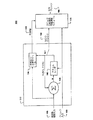
図1は、本発明の1実施例に従って、NCOにより発生されるクロックのジッタを最小化させることが可能な位相平滑化システム100のブロック図である。NCOクロックジッタは、NCO110に続くクロック位相選択可能遅延モジュールの付加によって減少される。NCOクロックジッタは、以下により詳細に説明する選択可能係数Lによって従来のNCOシステムにおける入力クロックの1クロック周期から減少される。
FIG. 1 is a block diagram of a
位相平滑化システム100は、選択可能な周波数における複数個のNCOクロックパルスを有するNCOクロック180を発生する形態とされているNCO110を有している。該NCOクロックは、入力クロック160及び基準入力、即ち周波数制御入力150、に基づいている。NCOクロック180は非常に精密な平均クロック周波数を発生するが、NCOクロック180はこの点においてクロックのサイクル毎のジッタを示している。即ち、NCOクロック180の複数個のNCOクロックパルスのエッジ(例えば、前端)は入力クロック160のエッジに整合されている。そうであるから、結果的に発生するジッタは入力クロック160の周期、例えばTckin、と等しい。
The
1実施例においては、NCO110は、入力クロック160を受け取り且つ入力クロックの前端において前の蓄積した値(例えば、N−1)を与える形態とされているアキュムレータ140を有している。該アキュムレータの出力は加算ブロック及び位相エラー計算モジュール130へ送られる。例示目的のために、本発明の実施例は入力クロック160のリーディングエッジ即ち前端でトリガーされるものとして説明する。然しながら、その他の実施例は、入力クロック160のフォーリングエッジ即ち後端でトリガーされる場合にも適している。
In one embodiment, the NCO 110 includes an
加算ブロック120はアキュムレータ140へ結合されており且つ入力クロックのエッジにおいて前の蓄積した値(例えば、N−1)を周波数制御入力150と加算する形態とされている。加算ブロック120はアキュムレータ140内に格納するために次の前に蓄積した値(例えば、N)を発生する。
Summing
その結果、アキュムレータ140は、入力クロックの各前端において格納されている値と周波数制御入力150とを断続的に加算する。その結果、アキュムレータ140は、NCOクロック180の複数個のNCOクロックパルスを発生することが可能である。特に、1実施例においては、アキュムレータ140は、該アキュムレータ内の蓄積された値に基づいてNCOクロックパルス(例えば、N−1)を発生する。1実施例においては、アキュムレータ140は1ビットの蓄積された値に基づいてNCOクロックパルスを発生する。別の実施例においては、アキュムレータ140はアキュムレータ140によって出力される蓄積された値の最大桁ビット(MSB)に基づいてNCOクロックパルスを発生する。更に別の実施例においては、アキュムレータ140は、MSBが1である場合にNCOクロックパルスを発生する。
As a result, the
特に、NCO110の平均出力周波数は以下のように式1で与えられる。
In particular, the average output frequency of the
![]()
![]()
式1において、以下の項、
In
![]()
![]()
はHzでのNCO出力180平均周波数を意味している。又、以下の項、
![]()
![]()
はHzでの入力クロック160周波数を意味している。以下の項、
Means the
![]()
![]()
はアキュムレータ140の大きさを意味しており、それは、1実施例においては、2の冪である(例えば、MNCO=2N)。又、以下の項、
Means the size of the
![]()
![]()
はアキュムレータ140内のビット数を意味している。以下の項、
Means the number of bits in the
![]()
![]()
はNCO周波数制御入力150を意味している。
Means the NCO
NCO110は、又、位相エラー計算モジュール130を有している。1実施例においては、位相エラー計算モジュールはアキュムレータ140へ結合されており且つアキュムレータ140の出力(例えば、N−1)を受け取る形態とされている。NCOクロック180の各パルスに対して、該位相エラー計算モジュールは対応する位相エラーを発生する形態とされている。
The
特に、位相エラー計算モジュール130はセレクト入力SCOMP135を発生し、それはNCOクロックパルス(例えば、N−1)の対応する位相エラーを表している。このセレクト入力は、NCOクロック180のジッタを減少させるためにNCOクロックパルスへ適用される位相遅延を発生するために使用される。
In particular, the phase
1実施例において、位相エラー計算モジュール130は、アキュムレータ140によって発生されるNCOクロックパルス(例えば、N−1)の位相エラーを決定する形態とされている。該位相エラーは、以下に更に詳細に説明するように、NCOクロックパルスの実際の位相を選択可能な周波数においての理想的なNCOクロックの位相と比較することによって決定される。付加的に、該位相エラーは、1実施例においては、アキュムレータ140内の蓄積された値のフラクショナルビット(fractional bits)に基づいており、又は、別の実施例によれば、アキュムレータ140内の蓄積された値と周波数制御入力150との結合に基づいている。
In one embodiment, the phase
1実施例においては、遅延パイプラインが位相エラー計算モジュールの後に導入される。該遅延パイプラインは、クロック入力の少なくとも一つの位相を有しており且つ出力クロック190に一様に適用される。該遅延パイプラインは、1実施例においては、位相エラー計算モジュール130がその計算を実行することを可能とするために導入される。
In one embodiment, a delay pipeline is introduced after the phase error calculation module. The delay pipeline has at least one phase of the clock input and is applied uniformly to the
位相平滑化システム100は、又、クロック位相選択可能遅延170を有しており、それは位相エラー計算モジュール130へ結合されている。クロック位相選択可能遅延170は、選択可能周波数においてジッタを減少させた出力クロックを発生するために、それに対応する位相エラー(例えば、位相エラー計算モジュール130によって発生されるセレクト入力)に従ってNCOクロック180の複数個のNCOクロックパルスの各々を調節する形態とされている。特に、該出力クロックの前端は入力クロックの前端と必ずしも整合するものではない。より特定的には、出力クロックのエッジは理想的な出力位相に一層近く近似すべく位相調節されており、入力クロックのエッジと必ずしも整合することは必要ではない。
The
特に、NCO110によって発生されるNCOクロックパルスの位相エラーは以下の如くに決定される。任意の与えられた時間において、アキュムレータ140の値は、以下の式2によって表されるように、デジタル形式におけるNCOクロックパルス(例えば、N−1)の位相を表すものと考えることが可能である。
In particular, the phase error of the NCO clock pulse generated by the

式2において、A(t)はアキュムレータ140の瞬間的な値である。1実施例においては、NCOクロック180はアキュムレータ140のMSBであるから、このことは真の位相の大雑把な近似と考えることが可能であり、それは180度の分解能での正確度である。
In
式1から、該アキュムレータの増分的正規化された位相変化は以下の式3によって与えられる。
From
これは、又、NCOクロックエッジが発生する位相エラーの上限である。NCOクロック180の全てのエッジにおいて、対応するNCOクロックパルスの正規化された位相エラーは以下の式4によって与えられる。
This is also the upper limit of the phase error that causes the NCO clock edge. At every edge of the
![]()
![]()
付加的に、対応するNCOクロックパルスの実際の位相は、1実施例においては、アキュムレータ140のフラクショナルビットから決定することが可能である。フラクショナルビット(AFRAC)は、アキュムレータ140内のMSB未満の値全てである。実際の位相は以下の式5によって与えられる。
Additionally, the actual phase of the corresponding NCO clock pulse can be determined from the fractional bits of
該実際の位相は、1実施例においては、NCOクロック180のエッジの離散化によって発生される位相エラーを取除くために使用される。特に、式5は正規化された位相エラーを表しており、それは理想的なクロックエッジ(例えば、0度)とNCO110によって発生されたNCOクロック180のNCOクロックパルスの実際の位相との間の差である。これはNCOクロック周波数に対して正規化される。然しながら、この位相エラーは式4によって拘束されるので、該位相エラーの補償はこの境界内において必要であるに過ぎない。そうであるから、該位相エラーは以下の式6における入力クロック周期に関しての正規化されたエラーとして表される。
The actual phase is used in one embodiment to remove the phase error caused by discretization of the
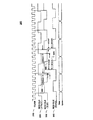
図3は、本発明の1実施例に従うシステム100によって発生される信号のタイミングを例示したタイミング線図300である。例えば、図3はクロック入力信号(CLKIN)310のタイミングを例示している。又、実際のNCOクロック(NCO CLK)320が示されている。1実施例においては、実際のNCO CLKは図1のNCOクロック180に類似している。更に、図3は、又、NCO110によって発生された位相エラーを補償する補償されたNCOクロック(NCO CLK)340を例示している。
FIG. 3 is a timing diagram 300 illustrating the timing of signals generated by the
特に、式6において計算される位相エラーは、理想的なNCO CLK320とNCO CLK330の実際のクロック位相との間の位相差を例示している。例えば、該差異はφERRCLK350で示されている。
In particular, the phase error calculated in Equation 6 illustrates the phase difference between the
式6において計算された正規化されたエラー(例えば、φERRCLK350)は、実際のNCO CLK330の実際の位相における「遅れ」を表している。この遅れが発生する理由は、ゼロのエラーは、実際のNCO CLK330のNCOクロックエッジはそれが理想的なNCO CLK320において理想的であるべき箇所に正確に発生することを暗示しているからである。そうであるから、正のエラーは、実際のNCO CLK330からの実際のNCOクロックエッジは式6において計算される位相エラーに等しい量だけ理想的なものより遅れて発生することを示している。1実施例においては、式6において計算されるこの位相エラーを補償するために、以下の式7において計算されるように、1−位相エラーである位相遅延を付加することが必要である。
The normalized error calculated in Equation 6 (eg, φ ERRCLK 350) represents the “lag” in the actual phase of the
![]()
![]()
式7において計算される補償された位相エラーは図3においてφCOMP360として示してある。
The compensated phase error calculated in
更に、図3に示されているように、NCO位相補償の位相遅延は、以下の式8に示されるように、一定とさせることが可能である。 Further, as shown in FIG. 3, the phase delay of the NCO phase compensation can be made constant as shown in Equation 8 below.
![]()
![]()
全位相φCOMP370も一定のものとして図3に示してある。式8に示されるように、NCO110の離散化によって導入される位相エラーに拘わらずに、この位相エラーは、最小のジッタ又はジッタ無しでの固定した位相遅延を発生させるための補償スキームによって取除くことが可能である。
The
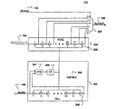
次に図2を参照すると、本発明の1実施例に基づくクロック位相選択可能遅延(CPSD)モジュール170のブロック線図が一層詳細に例示されている。CPSDモジュール170は、位相エラー計算モジュールによって出力されるセレクト入力SCOMP135に基づくNCOクロック180のNCOクロックパルス(例えば、N−1)の位相遅延させたバージョンを発生する。
Referring now to FIG. 2, a block diagram of a clock phase selectable delay (CPSD)
CPSDモジュール170は、式7における位相補償を発生する。CPSDモジュール170は、入力クロック160を受け取る形態とされている遅延ロックループ(DLL)240を有している。特に、DLL240は、1実施例においては、入力クロック160をL個の等しい位相へロックする。即ち、該LDDは、入力クロック160の周期TckinのL個の等しい位相がバッファLによって示されているようにバッファストリング245内の遅延ステージによって表されるように、入力クロック160をロックする。
特に、入力クロック160は、位相周波数検知器(PFD)247及びチャージポンプ249によって断続的にロックされる。即ち、PFD247はバッファのストリング245へ結合されており且つL個の等しい位相が入力クロック周期Tckinと等しく無い場合の位相エラーを計算する形態とされている。更に、チャージポンプ249はPFD147へ結合されており且つバッファのストリング245を入力クロックへロックさせるためにその差を補正する形態とされており、そのことは、入力クロック周期TckinにわたりL個の等しく離隔された位相を発生する。
In particular, the
更に、CPSDモジュール170は、アキュムレータ140へ結合されている電圧制御型遅延線(VCDL)230を有している。VCDL230は、NCOクロック180の複数個のNCOクロックパルスを受け取る形態とされている。更に、VCDL230は、入力クロック周期TckinのL個の等しい位相を発生する形態とされている。即ち、DLL240は、VCDL230におけるバッファLによって表されるバッファストリング235の遅延ステージを横断しての電圧を制御する制御型電圧245を発生する。
In addition,
VCDL235は、DLL240におけるバッファストリング235と同一であり且つマッチングする遅延ステージをバッファストリング235内に有している。そうであるから、VCDL230は、その遅延が1個の入力クロック周期Tckinと正確に等しく且つその位相が各々Tckin/Lによって表される遅延線を形成している。
The
CPSDモジュール170は、又、位相エラー計算モジュール130へ結合されているマルチプレクサ190を有している。該マルチプレクサは、入力NCOクロックパルス(例えば、N−1)の対応する位相エラーを受け取り且つ該対応する位相エラーに基づいて適宜の位相遅延を選択する形態とされている。該適宜の位相遅延は、出力クロック190を発生するために、前記複数個のNCOクロックパルスの内の対応するNCOクロックパルス(例えば、N−1)へ適用される。
特に、該NCOクロックパルス(例えば、N−1)は、前述したように、セレクト信号SCOMP135から選択される適宜の位相遅延でVCDL235を介して通過される。即ち、1実施例においては、該マルチプレクサは、該バッファストリング235内の適宜のタップ点を選択して、適宜の位相遅延をNCOクロックパルス(例えば、N−1)へ付加してジッタを減少させる。
In particular, the NCO clock pulse (eg, N-1) is passed through the
1実施例においては、使用可能な位相選択の数は離散的であるので、式7の位相補償は、SCOMP135を発生させるために式9において修正される。
In one embodiment, since the number of phase selections available is discrete, the phase compensation of
![]()
![]()
式9において、1実施例においては、SCOMPは最も近い整数値へ切り捨てられる。図2に示されているように、SCOMPのより低い値は一層大きな位相遅延を選択して式7の逆の関係を実現する。本発明の実施例においては、全体的なシステムのジッタ要件を満足させるためにバッファストリング235の遅延線内に位相タップの数を増加させるためにLを変化させることが可能である。
In Equation 9, in one embodiment, S COMP is rounded down to the nearest integer value. As shown in FIG. 2, a lower value of S COMP selects a larger phase delay to achieve the inverse relationship of
別の実施例においては、出力クロック190はグリッチが無いものであるように構成されている。特に、セレクト入力SCOMPは、VCDLバッファストリング235の要素の全てが同一の値(例えば、全て低)にある場合にのみ変化される。1実施例において、マルチプレクサ220がこれらの条件下においてグリッチの無いものである場合には、出力クロック190におけるジッタは最小化されており且つグリッチの無いものである。
In another embodiment,
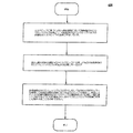
図4は、本発明の1実施例に従ってNCOクロックに対して位相平滑化を与える方法における段階を例示しているフローチャート400である。即ち、本実施例は、NCOによって発生される出力クロックにおけるジッタを最小化させる。
FIG. 4 is a
410において、本実施例は入力クロックに基づく選択可能周波数において複数個のNCOクロックパルスを発生する。特に、NCO110は選択可能周波数において複数個のNCOクロックパルスを発生する。該複数個のNCOクロックパルスの前端は入力クロックの前端と整合されている。
At 410, the present embodiment generates a plurality of NCO clock pulses at a selectable frequency based on the input clock. In particular, the
更に詳細には、入力クロックの前端において、本実施例は、前の蓄積した値を周波数制御入力と加算して現在の蓄積された値を発生する。この現在の蓄積された値は、入力クロックの次の前端によって導入される次のサイクルに対する次の前に蓄積された値を有している。 More specifically, at the leading edge of the input clock, the present embodiment adds the previous accumulated value with the frequency control input to generate the current accumulated value. This current accumulated value has the next previously accumulated value for the next cycle introduced by the next leading edge of the input clock.
又、本実施例は、該前の蓄積された値のMSBが1である場合に該複数個のNCOクロックパルスの内の1個のNCOクロックパルスを発生する。即ち、図1のアキュムレータ140内の蓄積された値のMSBが1の値をアサートする場合にはいつでも、該アキュムレータはNCOクロックパルス(例えば、N−1)を発生する。
In this embodiment, when the MSB of the previous accumulated value is 1, one NCO clock pulse is generated from the plurality of NCO clock pulses. That is, whenever the stored value MSB in the
420において、本実施例は、該複数個のNCOクロックパルスの各々に対しての対応する位相エラーを決定する。特に、位相エラー計算モジュール130は位相エラーを決定する。該位相エラーは、対応するNCOクロックパルスの実際の位相を選択可能周波数の理想的なNCOクロックの理想的な位相と比較することにより計算される。
At 420, the present embodiment determines a corresponding phase error for each of the plurality of NCO clock pulses. In particular, the phase
特に、本実施例は、周波数制御入力及び前の蓄積した値のフラクショナルビットに基づいてNCOクロックパルスの正規化された位相エラーを決定する。該正規化された位相エラーは、1から該正規化された位相エラーを減算して対応するNCOクロックパルスの対応する位相エラーを発生させることにより補償される。 In particular, the present embodiment determines the normalized phase error of the NCO clock pulse based on the frequency control input and the fractional bit of the previous accumulated value. The normalized phase error is compensated by subtracting the normalized phase error from 1 to generate the corresponding phase error of the corresponding NCO clock pulse.
430において、本実施例は、該対応する位相エラーを該複数個のNCOクロックパルスの各々へ適用する。特に、CPSDモジュール170は、該対応する位相エラーを適用して選択可能周波数における出力クロックを発生し、そのことはジッタを最小化させる。特に、出力クロックの前端は入力クロックの前端に必ずしも整合していることは必要ではない。
At 430, the present embodiment applies the corresponding phase error to each of the plurality of NCO clock pulses. In particular,
特に、本実施例は、入力クロックのL個の等しい位相に対応するL個のタップ点、又はVCDLにおける例を有している遅延線を形成している。即ち、入力クロックは、例えば、VCDLを制御するDLLにおいて、L個の等しい位相へロックされる。NCOクロックパルスを受け取った後に、本実施例は、対応するNCOクロックパルスに対して適宜の位相遅延を適用するために対応する位相エラーに基づいて該遅延線内の適宜のタップ点を選択することが可能である。その後に、本実施例は、出力クロックの一部として適宜の位相遅延を具備する対応するNCOクロックパルスを出力することが可能である。 In particular, this embodiment forms L tap points corresponding to L equal phases of the input clock, or a delay line having an example in VCDL. That is, the input clock is locked to L equal phases, for example, in the DLL that controls the VCDL. After receiving an NCO clock pulse, the present embodiment selects an appropriate tap point in the delay line based on the corresponding phase error to apply an appropriate phase delay to the corresponding NCO clock pulse. Is possible. Thereafter, this embodiment can output a corresponding NCO clock pulse with an appropriate phase delay as part of the output clock.
要するに、フローチャート400の方法は、VCDL230を制御するDLL240から構成されているCPSDモジュール170を使用する。CPSDモジュール170は、CPSDモジュール170に対するセレクト入力によって選択される入力クロック周期TckinのL個の等しく離隔された遅延を発生する。該適宜の遅延は、全てのNCOクロック出力に関するNCOフラクショナルビットに基づいて選択される。CPSD機能の出力は、i×Tckinだけ遅延された出力クロックであり、尚i=0,1,...,L−1である。そうであるから、このことは、1実施例においては、NCOクロックジッタをTckinからTckin/Lへ減少させる所望の効果を具備している。
In short, the method of
広義には、本記載は出力クロック位相平滑化を実施するシステム及び方法を開示している。位相平滑化回路を記載しており、それは入力クロックに基づいている選択可能周波数において複数個のNCOクロックパルスを発生する形態とされている数値制御型オシレータ(NCO)を包含している。該複数個のNCOクロックパルスのエッジは入力クロックのエッジに対して整合される。位相エラー計算モジュールがNCOへ結合されており且つ該複数個のNCOクロックパルスの各々に対して対応する位相エラーを発生する形態とされている。クロック位相選択可能遅延が該位相エラー計算モジュールへ結合されており且つ一層近接して理想的な出力クロック位相と整合するように位相調節された選択可能周波数における出力パルスを発生するために、対応する位相エラーに従って該複数個のNCOクロックパルスの各々を調節する形態とされている。出力クロックのエッジは入力クロックのエッジに対して必ずしも整合していることは必要ではない。 In a broad sense, this description discloses a system and method for performing output clock phase smoothing. A phase smoothing circuit is described, which includes a numerically controlled oscillator (NCO) configured to generate a plurality of NCO clock pulses at a selectable frequency based on an input clock. The edges of the plurality of NCO clock pulses are aligned with the edges of the input clock. A phase error calculation module is coupled to the NCO and is configured to generate a corresponding phase error for each of the plurality of NCO clock pulses. A clock phase selectable delay is coupled to the phase error calculation module and corresponding to generate an output pulse at a selectable frequency that is phase adjusted to more closely match the ideal output clock phase. Each of the plurality of NCO clock pulses is adjusted according to a phase error. The edge of the output clock is not necessarily aligned with the edge of the input clock.
従って、本発明の種々の実施例はNCO出力クロック位相平滑化を実施するためのシステム及び方法を開示している。本発明の実施例は、上の成果を与え且つ更にNCOによって発生される出力クロック信号におけるジッタを最小化させることを与える。 Accordingly, various embodiments of the present invention disclose systems and methods for performing NCO output clock phase smoothing. Embodiments of the present invention provide the above results and further minimize jitter in the output clock signal generated by the NCO.
本発明の実施例、NCOによって発生されるクロックにおけるジッタを最小化させるためのシステム及び方法を記載している。本発明は好適実施例に関連して記載してあるが、本発明をこれらの実施例に制限することを意図したものでないことが理解される。それとは反対に、本発明は特許請求の範囲によって定義されるように、本発明の精神及び範囲内に包含される場合のある変形例、修正例、及び均等物をカバーするものであることが意図されている。更に、本発明の詳細な説明においては、本発明の完全なる理解を与えるために多数の特定的な詳細について記載されている。然しながら、当業者によって認識されるように、本発明はこれらの特定的な詳細無しで実施することも可能である。その他の場合において、周知の方法、手順、コンポーネント、及び回路については詳細に記載していないが、本発明の側面を不必要にぼかすことがないためである。 Embodiments of the present invention describe a system and method for minimizing jitter in a clock generated by an NCO. While the invention has been described in connection with preferred embodiments, it will be understood that it is not intended to limit the invention to these embodiments. On the contrary, the invention is intended to cover variations, modifications, and equivalents that may be included within the spirit and scope of the invention as defined by the claims. Is intended. Furthermore, in the detailed description of the present invention, numerous specific details are set forth in order to provide a thorough understanding of the present invention. However, it will be appreciated by those skilled in the art that the present invention may be practiced without these specific details. In other instances, well known methods, procedures, components, and circuits have not been described in detail as not to unnecessarily obscure aspects of the present invention.
Claims (17)
入力クロックに基づく選択可能周波数において複数個のNCOクロックパルスを生成するように構成されており、前記複数個のNCOクロックパルスのエッジが前記入力クロックのエッジに整合されている、数値制御型オシレータ(NCO)と、
前記NCOへ結合されており、前記複数個のNCOクロックパルスの各々に対して対応する位相エラーを生成するように構成されている、位相エラー計算モジュールと、
前記位相エラー計算モジュールへ結合されており、前記選択可能周波数において出力クロックを発生するために前記対応する位相エラーに従って前記複数個のNCOクロックパルスの各々を調節するように構成されているクロック位相選択可能遅延であって、前記出力クロックのエッジが、理想的な出力位相を一層近接して近似するべく位相調節されており且つ前記入力クロックの前記エッジと必ずしも整合する必要がない、クロック位相選択可能遅延と、
を含み、
前記クロック位相選択可能遅延が、
L個のバッファの第1のストリングを有し、前記入力クロックを受け取り且つ前記入力クロックをL個の等しい位相へロックするように構成されている遅延ロックループ(DLL)と、
L個のバッファの第2のストリングを有し、前記複数個のNCOクロックパルスを受け取り且つ前記入力クロックの前記L個の等しい位相を発生するように構成されている電圧制御型遅延線(VCDL)と、
前記対応する位相エラーを受け取り且つ前記複数個のNCOクロックパルスの内の対応するNCOクロックパルスへ適用される前記対応する位相エラーに基づいて適宜の位相遅延を選択するように構成されているマルチプレクサと、
を含み、
L個のバッファの前記第2のストリングに印加される制御電圧がL個のバッファの前記第1のストリングに印加される制御電圧と等しい、
位相平滑化システム。It met phase smoothing system,
A numerically controlled oscillator configured to generate a plurality of NCO clock pulses at selectable frequencies based on an input clock, wherein edges of the plurality of NCO clock pulses are aligned with edges of the input clock ( and NCO),
Is coupled to the NCO, is configured to produce a corresponding phase error has for each of said plurality of NCO clock pulses, a phase error computing module,
A clock phase selection coupled to the phase error calculation module and configured to adjust each of the plurality of NCO clock pulses according to the corresponding phase error to generate an output clock at the selectable frequency can be a delay, an edge of the output clock, the ideal is not always necessary to align with the phase adjusted to have and the edge of the input clock to be more close to approximating the output phase, the clock phase can be selected With delay,
Including
The clock phase selectable delay is
A delay locked loop (DLL) having a first string of L buffers, configured to receive the input clock and lock the input clock to L equal phases;
A voltage controlled delay line (VCDL) having a second string of L buffers, configured to receive the plurality of NCO clock pulses and generate the L equal phases of the input clock When,
A multiplexer configured to receive the corresponding phase error and to select an appropriate phase delay based on the corresponding phase error applied to a corresponding NCO clock pulse of the plurality of NCO clock pulses; ,
Including
A control voltage applied to the second strings of L buffers is equal to a control voltage applied to the first strings of L buffers;
Phase smoothing system.
前記NCOが、
前記入力クロックを受け取り且つ前記入力クロックのエッジにおいて蓄積された値を与えるように構成されているアキュムレータを含む、
位相平滑化システム。 The phase smoothing system of claim 1,
The NCO is
Comprising an accumulator configured to provide accumulated values in the input clock to receive and of the input clock edge,
Phase smoothing system.
前記NCOが、更に、
前記アキュムレータへ結合されており、前記アキュムレータ内の値を周波数制御入力に継続的に加算するように構成されている加算ブロックを含む、
位相平滑化システム。 The phase smoothing system according to claim 2,
Said NCO further,
Is coupled to said accumulator comprises a summing block configured to continuously adding the value in the accumulator to the frequency control input,
Phase smoothing system.
前記加算ブロックが、前記入力クロックの前記エッジにおいて前記周波数制御入力を前記蓄積された値に加算し且つ前記アキュムレータ内に格納するために次の前に蓄積された値を発生するように構成されている、位相平滑化システム。 The phase smoothing system according to claim 3,
The addition block, is configured to generate the stored value before the next in order to store the frequency control input to the added to the accumulated value and the said accumulator in said edge of said input clock There is a phase smoothing system.
前記アキュムレータが、前記複数個のNCOクロックパルスの内の1個のNCOクロックパルスを出力するように構成されている、位相平滑化システム。 The phase smoothing system according to claim 2,
Said accumulator, one is configured to output the NCO clock pulse, the phase smoothing system of said plurality of NCO clock pulses.
前記位相エラー計算モジュールが、前記選択可能周波数において理想的なNCOクロックと比較される前記アキュムレータによって発生されるNCOクロックパルスの位相エラーを決定するように構成されており、前記位相エラーが前記アキュムレータ内の前記蓄積された値のフラクショナルビットに基づいている、位相平滑化システム。 The phase smoothing system according to claim 2,
It said phase error calculation module, said selectable frequency is configured to determine a phase error of an ideal NCO clock pulses that will be generated by the accumulator is compared to the NCO clock in the phase error in the accumulator wherein based on the fractional bits of the accumulated value, the phase smoothing system.
前記DLLが、
前記第1のストリングに結合されており、前記Lに等しい位相が入力クロック周期に等しく無い場合に差エラーを計算するように構成されている位相周波数検知器(PFD)と、
前記ストリングを前記入力クロックへロックするために前記差エラーを補正するために前記PFDへ結合されているチャージポンプと、
を含む、位相平滑化システム。 The phase smoothing system of claim 1 ,
The DLL is
Wherein and are bonded to the first string, the phase frequency detector L equal phase is configured to calculate the difference error if not equal to the input clock period and (PFD),
A charge pump the coupled to the PFD to correct the difference error the string in order to lock to the input clock,
Including a phase smoothing system.
入力クロックを受け取り且つ前記入力クロックのエッジにおいて蓄積された値を供給するように構成されており、選択可能周波数においてNCOクロックのNCOクロックパルスを生成する、アキュムレータと、
前記アキュムレータへ結合されており、前記アキュムレータ内に格納するために次の蓄積された値を発生するために前記蓄積された値を周波数制御入力に加算するように攻勢されている、加算ブロックと、
前記アキュムレータへ結合されており、前記NCOクロックパルスに対する位相エラーを発生するように構成されている、位相エラー計算モジュールと、
前記位相エラー計算モジュールへ結合されており、前記選択可能周波数において出力クロックの出力クロックパルスを発生するために前記位相エラーに従って前記NCOクロックパルスを調節するように構成されているクロック位相選択可能遅延であって、前記出力クロックのエッジが理想的な出力位相を一層近接して近似するように位相調節されており且つ前記入力クロックの前記エッジに必ずしも整合する必要がない、クロック位相選択可能遅延と、
を含み、
前記クロック位相選択可能遅延が、
L個のバッファの第1のストリングを有し、前記入力クロックを受け取り且つ前記入力クロックをL個の等しい位相へロックするように構成されている遅延ロックループ(DLL)と、
L個のバッファの第2のストリングを有し、前記NCOクロックパルスを受け取り且つ前記入力クロックの前記L個の等しい位相を発生するように構成されている電圧制御型遅延線(VCDL)と、
前記位相エラーを受け取り且つ前記出力クロックとして前記NCOクロックパルスへ印加される前記位相エラーに基づいて適宜の位相遅延を選択するように構成されているマルチプレクサと、
を含み、
L個のバッファの前記第2のストリングに印加される制御電圧がL個のバッファの前記第1のストリングに印加される制御電圧と等しい、
位相平滑化システム。It met phase smoothing system,
The accumulated value in the receive input clock and the input clock edge is configured for supplying, to produce an NCO clock pulses of the NCO clock at selectable frequencies, and the accumulator,
Said accumulator is coupled to, and is offensive to be summed the accumulated value to generate the next accumulated values for storage in said accumulator to a frequency control input, and the addition block ,
Is coupled to the accumulator, and is configured to generate a phase error with respect to the NCO clock pulse, the phase error calculation module,
In the is coupled to the phase error calculation module, said selectable wherein the NCO clock pulse modulate so Configured clock phase selectable delay according to the phase error to generate the output clock pulses of the output clock at a frequency there are, edges of the output clock does not need to be necessarily aligned with the phase adjustment has been provided and the edge of the input clock to more closely to approximate the ideal output phase, the clock phase selectable delay,
Including
The clock phase selectable delay is
A delay locked loop (DLL) having a first string of L buffers, configured to receive the input clock and lock the input clock to L equal phases;
A voltage controlled delay line (VCDL) having a second string of L buffers, configured to receive the NCO clock pulse and generate the L equal phases of the input clock;
A multiplexer configured to receive the phase error and to select an appropriate phase delay based on the phase error applied to the NCO clock pulse as the output clock;
Including
A control voltage applied to the second strings of L buffers is equal to a control voltage applied to the first strings of L buffers;
Phase smoothing system.
前記位相エラー計算モジュールが前記蓄積された値のフラクショナルビットに基づいて前記位相エラーを決定するように構成されている、位相平滑化システム。 The phase smoothing system according to claim 8 , comprising:
Said phase error calculation module is configured to determine that the phase error based on the fractional bits of the accumulated value, the phase smoothing system.
前記アキュムレータが前記蓄積された値の1個のビットに基づいて前記NCOクロックパルスを生成する、位相平滑化システム。 The phase smoothing system according to claim 8 , comprising:
The accumulator generates the NCO clock pulse based on one bit of said accumulated value, the phase smoothing system.
入力クロックに基づく選択可能周波数において複数個のNCOクロックパルスを生成し、前記複数個のNCOクロックパルスの前端が前記入力クロックの前端に整合しており、
前記選択可能周波数の理想的なNCOクロックと比較された場合に前記複数個のNCOクロックパルスの各々に対する対応する位相エラーを決定し、
前記選択可能周波数において出力クロックを発生するために前記対応する位相エラーを前記複数個のNCOクロックパルスの各々へ適用し、前記出力クロックの前記前端が前記理想的なNCOクロックの理想的な位相に一層近接して近似するように位相調節されており且つ前記入力クロックの前記前端と必ずしも整合する必要がない、
ことを含み、
前記対応する位相エラーを適用することが、
前記入力クロックのL個の等しい位相に対応するL個のタップ点を含む第1の遅延線を形成し、
前記NCOクロックパルスのL個の等しい位相に対応するL個のタップ点を含む第2の遅延線を形成し、
前記NCOクロックパルスへ適宜の位相遅延を適用するために前記対応する位相エラーに基づいて前記第2の遅延線の適宜のタップ点を選択する、
ことを含み、
前記第1及び第2の遅延線が同じ制御電圧で制御される、
方法。We met how to provide a phase smoothing,
Generating a plurality of NCO clock pulses at a selectable frequency based on the input clock, the front end of the plurality of NCO clock pulses are aligned with the front end of the input clock,
Determining a corresponding phase error for each of the plurality of NCO clock pulses when compared to an ideal NCO clock of the selectable frequency;
Applying the corresponding phase error to generate an output clock at said selectable frequency to each of said plurality of NCO clock pulses, the ideal phase of the front end of the output clock is the ideal NCO clock there is no need to always aligned with the front end of the phase-adjusted and and the input clock to approximate to further close,
Including
Applying the corresponding phase error,
Forming a first delay line including L tap points corresponding to L equal phases of the input clock;
Forming a second delay line including L tap points corresponding to L equal phases of the NCO clock pulse;
Selecting an appropriate tap point of the second delay line based on the corresponding phase error to apply an appropriate phase delay to the NCO clock pulse;
Including
The first and second delay lines are controlled by the same control voltage;
Method.
前記複数個のNCOクロックパルスを生成することが、
前記入力クロックの前端において、蓄積された値を周波数制御入力に加算して次の蓄積された値を発生し、
前記次の蓄積された値を格納する、
ことを含む、方法。 The method of claim 11 , comprising:
Generating the plurality of NCO clock pulses;
In front of the input clock, the accumulated value is added to the frequency control input to generate the next accumulated value,
Storing said next of the accumulated value,
Including the method.
前記複数個のNCOクロックパルスの内の1個のNCOクロックパルスを発生する、
ことを含む、方法。 The method of claim 12 , further comprising:
Generating one NCO clock pulse of the plurality of NCO clock pulses;
Including the method.
前記対応する位相エラーを決定することが、
前記蓄積された値のフラクショナルビットに基づいてNCOクロックパルスの正規化された位相エラーを決定し、
1から前記正規化された位相エラーを減算することにより前記対応する位相エラーを発生するために前記正規化された位相エラーを補償する、
ことを含む、方法。 The method of claim 12 , comprising:
Determining the corresponding phase error;
Wherein determining a normalized phase error of the NCO clock pulse based on fractional bits of the accumulated value,
Wherein compensating the normalized phase error to generate the corresponding phase error by subtracting the normalized phase error from 1,
Including the method.
前記入力クロックを受け取り、
前記入力クロックをL個の等しい位相へロックする、
ことを含む、方法。 The method of claim 11 , further comprising:
Receiving the input clock;
Lock the input clock to L equal phases;
Including the method.
前記出力クロックとして前記適宜の位相遅延を具備する前記NCOクロックパルスを出力する、
ことを含む、方法。 The method of claim 11 , further comprising:
Outputting the NCO clock pulse having the appropriate phase delay as the output clock;
Including the method.
前記適宜のタップ点を選択することが、
前記L個のタップ点を提供する電圧制御型遅延線(VCDL)の全てのバッファが同一の値である場合に前記適宜のタップ点を選択する、
ことを含む、方法。 The method of claim 11 , comprising:
Selecting the appropriate tap point,
Wherein selecting a tap point in the appropriate case all the buffers of the L that provides tap point voltage controlled delay lines (VCDL) are the same value,
Including the method.
Applications Claiming Priority (3)
| Application Number | Priority Date | Filing Date | Title |
|---|---|---|---|
| US11/523,123 US7826582B2 (en) | 2006-09-18 | 2006-09-18 | Numerically controlled oscillator (NCO) output clock phase smoothing |
| US11/523,123 | 2006-09-18 | ||
| PCT/US2007/078688 WO2008036613A1 (en) | 2006-09-18 | 2007-09-18 | Numerically controlled oscillator (nco) output clock phase smoothing |
Publications (2)
| Publication Number | Publication Date |
|---|---|
| JP2010504068A JP2010504068A (en) | 2010-02-04 |
| JP5073749B2 true JP5073749B2 (en) | 2012-11-14 |
Family
ID=39188588
Family Applications (1)
| Application Number | Title | Priority Date | Filing Date |
|---|---|---|---|
| JP2009529327A Active JP5073749B2 (en) | 2006-09-18 | 2007-09-18 | Numerically controlled oscillator (NCO) output clock phase smoothing |
Country Status (5)
| Country | Link |
|---|---|
| US (1) | US7826582B2 (en) |
| JP (1) | JP5073749B2 (en) |
| KR (1) | KR20090067182A (en) |
| TW (1) | TWI441455B (en) |
| WO (1) | WO2008036613A1 (en) |
Families Citing this family (13)
| Publication number | Priority date | Publication date | Assignee | Title |
|---|---|---|---|---|
| US7907028B1 (en) * | 2008-02-19 | 2011-03-15 | Marvell International, Ltd. | Jitter compensated numerically controlled oscillator |
| US8082462B1 (en) * | 2008-11-13 | 2011-12-20 | Xilinx, Inc. | Direct synthesis of audio clock from a video clock via phase interpolation of a dithered pulse |
| KR20130111519A (en) * | 2010-06-10 | 2013-10-10 | 콘티넨탈 테베스 아게 운트 코. 오하게 | Speed sensor comprising a costas loop |
| CN102468845B (en) * | 2010-10-29 | 2013-10-16 | 鼎桥通信技术有限公司 | Method for eliminating frequency deviation of numerically controlled oscillator |
| DE102011003738B4 (en) | 2011-02-08 | 2018-12-27 | Robert Bosch Gmbh | A method and apparatus for reducing signal edge jitter in an output signal of a numerically controlled oscillator |
| US9024699B2 (en) | 2013-01-21 | 2015-05-05 | Apple Inc. | Numerically-controlled oscillator |
| KR101982492B1 (en) | 2013-01-25 | 2019-05-27 | 삼성전자 주식회사 | Method and apparatuses for generating a clock signal by normalizing duty code to period code |
| US9563227B2 (en) * | 2013-02-06 | 2017-02-07 | Nvidia Corporation | Approach to clock frequency modulation of a fixed frequency clock source |
| US9287884B2 (en) * | 2013-02-21 | 2016-03-15 | Microchip Technology Incorporated | Enhanced numerical controlled oscillator |
| US10061444B2 (en) * | 2013-07-31 | 2018-08-28 | Apple Inc. | Self capacitance touch sensing |
| US9590602B2 (en) * | 2014-06-13 | 2017-03-07 | Stmicroelectronics International N.V. | System and method for a pulse generator |
| US9577648B2 (en) | 2014-12-31 | 2017-02-21 | Semtech Corporation | Semiconductor device and method for accurate clock domain synchronization over a wide frequency range |
| US10156135B2 (en) | 2015-04-08 | 2018-12-18 | Halliburton Energy Services, Inc. | Phase compensated fixed-point numerically controlled oscillator for downhole logging |
Family Cites Families (14)
| Publication number | Priority date | Publication date | Assignee | Title |
|---|---|---|---|---|
| US5365182A (en) | 1993-06-22 | 1994-11-15 | Motorola, Inc. | Method and apparatus for low power clock generation for high speed applications |
| US6424185B1 (en) | 1998-05-22 | 2002-07-23 | National Semiconductor Corporation | NCO based frequency synthesizer with jitter modulation |
| US6650721B1 (en) | 1999-08-05 | 2003-11-18 | Agere Systems Inc. | Phase locked loop with numerically controlled oscillator divider in feedback loop |
| US6429693B1 (en) * | 2000-06-30 | 2002-08-06 | Texas Instruments Incorporated | Digital fractional phase detector |
| DE10033109C2 (en) * | 2000-07-07 | 2002-06-20 | Infineon Technologies Ag | Clock signal generator |
| US6983032B2 (en) * | 2001-08-28 | 2006-01-03 | Texas Instruments Incorporated | Digital timing recovery method for communication receivers |
| US7839178B2 (en) * | 2002-08-20 | 2010-11-23 | Seagate Technology Llc | High speed digital phase/frequency comparator for phase locked loops |
| JP3863522B2 (en) * | 2003-12-25 | 2006-12-27 | Necエレクトロニクス株式会社 | Digital VCO, VCO circuit, PLL circuit, information recording apparatus, and synchronous clock signal generation method |
| US7643595B2 (en) * | 2004-09-13 | 2010-01-05 | Nortel Networks Limited | Method and apparatus for synchronizing clock timing between network elements |
| KR100644127B1 (en) * | 2005-01-03 | 2006-11-10 | 학교법인 포항공과대학교 | Dual loop DL based on voltage controlled delay line with infinite phase shift |
| US7102403B2 (en) * | 2005-02-03 | 2006-09-05 | Mediatek Incorporation | Clock recovering circuit utilizing a delay locked loop for generating an output clock locked to an analog input signal and related method thereof |
| US7271634B1 (en) * | 2005-09-16 | 2007-09-18 | Advanced Micro Devices, Inc. | Delay-locked loop having a plurality of lock modes |
| US7323915B2 (en) * | 2006-01-19 | 2008-01-29 | Honeywell International, Inc. | Delay locked loop with selectable delay |
| US7570725B1 (en) * | 2006-03-07 | 2009-08-04 | Marvell International Ltd. | Numerically controlled oscillator |
-
2006
- 2006-09-18 US US11/523,123 patent/US7826582B2/en active Active
-
2007
- 2007-09-18 WO PCT/US2007/078688 patent/WO2008036613A1/en not_active Ceased
- 2007-09-18 KR KR1020097007839A patent/KR20090067182A/en not_active Withdrawn
- 2007-09-18 JP JP2009529327A patent/JP5073749B2/en active Active
- 2007-09-19 TW TW096134782A patent/TWI441455B/en active
Also Published As
| Publication number | Publication date |
|---|---|
| WO2008036613A1 (en) | 2008-03-27 |
| KR20090067182A (en) | 2009-06-24 |
| JP2010504068A (en) | 2010-02-04 |
| US20080069284A1 (en) | 2008-03-20 |
| TWI441455B (en) | 2014-06-11 |
| TW200838148A (en) | 2008-09-16 |
| US7826582B2 (en) | 2010-11-02 |
Similar Documents
| Publication | Publication Date | Title |
|---|---|---|
| JP5073749B2 (en) | Numerically controlled oscillator (NCO) output clock phase smoothing | |
| CN100409572C (en) | Frequency Converter and How to Use It | |
| US9735787B2 (en) | Frequency synthesizer with dynamic phase and pulse-width control | |
| US20100045395A1 (en) | Frequency adjustment for clock generator | |
| WO2010036449A2 (en) | Method and apparatus for counter-based clock signal adaptation | |
| US8184762B2 (en) | Digital phase lock loop with multi-phase master clock | |
| US6779010B2 (en) | Accumulator with programmable full-scale range | |
| US8664990B2 (en) | Coherent phase locked loop | |
| US12308850B2 (en) | Low jitter clock multiplier circuit and method with arbitrary frequency acquisition | |
| US7071787B2 (en) | Method and apparatus for the reduction of phase noise | |
| JP4198068B2 (en) | Method and apparatus for digital frequency conversion | |
| US20080068048A1 (en) | Fixed Frequency Clock Output Having A Variable High Frequency Input Clock And An Unrelated Fixed Frequency Reference Signal | |
| US8443023B2 (en) | Frequency synthesis rational division | |
| CN1951014A (en) | Apparatus and method for programmable clock generator | |
| JP2017169189A (en) | Spread spectrum clock generator | |
| KR20050016309A (en) | Method and apparatus for digital frequency conversion |
Legal Events
| Date | Code | Title | Description |
|---|---|---|---|
| A621 | Written request for application examination |
Free format text: JAPANESE INTERMEDIATE CODE: A621 Effective date: 20100909 |
|
| A977 | Report on retrieval |
Free format text: JAPANESE INTERMEDIATE CODE: A971007 Effective date: 20120412 |
|
| A131 | Notification of reasons for refusal |
Free format text: JAPANESE INTERMEDIATE CODE: A131 Effective date: 20120424 |
|
| A521 | Request for written amendment filed |
Free format text: JAPANESE INTERMEDIATE CODE: A523 Effective date: 20120627 |
|
| TRDD | Decision of grant or rejection written | ||
| A01 | Written decision to grant a patent or to grant a registration (utility model) |
Free format text: JAPANESE INTERMEDIATE CODE: A01 Effective date: 20120814 |
|
| A01 | Written decision to grant a patent or to grant a registration (utility model) |
Free format text: JAPANESE INTERMEDIATE CODE: A01 |
|
| A61 | First payment of annual fees (during grant procedure) |
Free format text: JAPANESE INTERMEDIATE CODE: A61 Effective date: 20120822 |
|
| R150 | Certificate of patent or registration of utility model |
Ref document number: 5073749 Country of ref document: JP Free format text: JAPANESE INTERMEDIATE CODE: R150 Free format text: JAPANESE INTERMEDIATE CODE: R150 |
|
| FPAY | Renewal fee payment (event date is renewal date of database) |
Free format text: PAYMENT UNTIL: 20150831 Year of fee payment: 3 |
|
| R250 | Receipt of annual fees |
Free format text: JAPANESE INTERMEDIATE CODE: R250 |
|
| R250 | Receipt of annual fees |
Free format text: JAPANESE INTERMEDIATE CODE: R250 |
|
| R250 | Receipt of annual fees |
Free format text: JAPANESE INTERMEDIATE CODE: R250 |
|
| R250 | Receipt of annual fees |
Free format text: JAPANESE INTERMEDIATE CODE: R250 |
|
| R250 | Receipt of annual fees |
Free format text: JAPANESE INTERMEDIATE CODE: R250 |
|
| R250 | Receipt of annual fees |
Free format text: JAPANESE INTERMEDIATE CODE: R250 |
|
| R250 | Receipt of annual fees |
Free format text: JAPANESE INTERMEDIATE CODE: R250 |
|
| R250 | Receipt of annual fees |
Free format text: JAPANESE INTERMEDIATE CODE: R250 |
|
| R250 | Receipt of annual fees |
Free format text: JAPANESE INTERMEDIATE CODE: R250 |
|
| R250 | Receipt of annual fees |
Free format text: JAPANESE INTERMEDIATE CODE: R250 |