JP5065725B2 - Plasma processing equipment - Google Patents
Plasma processing equipment Download PDFInfo
- Publication number
- JP5065725B2 JP5065725B2 JP2007078860A JP2007078860A JP5065725B2 JP 5065725 B2 JP5065725 B2 JP 5065725B2 JP 2007078860 A JP2007078860 A JP 2007078860A JP 2007078860 A JP2007078860 A JP 2007078860A JP 5065725 B2 JP5065725 B2 JP 5065725B2
- Authority
- JP
- Japan
- Prior art keywords
- plasma
- processing apparatus
- reaction chamber
- frequency power
- power source
- Prior art date
- Legal status (The legal status is an assumption and is not a legal conclusion. Google has not performed a legal analysis and makes no representation as to the accuracy of the status listed.)
- Active
Links
Images


Description
本発明は、プラズマを利用して、半導体基板やガラス基板のエッチング処理又は成膜処理を行うプラズマ処理装置に関し、更に詳しくは、磁場ゼロの環状磁気中性線と交番電場とを結合させてプラズマを発生させるプラズマエッチング装置に関する。 The present invention relates to a plasma processing apparatus that performs etching processing or film forming processing of a semiconductor substrate or a glass substrate using plasma, and more specifically, plasma is obtained by combining an annular magnetic neutral line having a zero magnetic field and an alternating electric field. The present invention relates to a plasma etching apparatus which generates
近年、プラズマを利用して基板のエッチング処理を行うプラズマエッチング装置が広く知られている。この種のプラズマエッチング装置としては、プラズマを発生させるプラズマ源の構成に応じて幾つかの方式に分類され、中でも、真空槽内に形成した電場と磁場との結合によりプラズマを発生させるようにしたプラズマエッチング装置が知られている。例えば特許文献1には、図6に示すプラズマエッチング装置10が開示されている。
In recent years, plasma etching apparatuses that perform etching of a substrate using plasma have been widely known. This type of plasma etching apparatus is classified into several methods depending on the configuration of the plasma source that generates the plasma. Among them, the plasma is generated by the combination of the electric field and the magnetic field formed in the vacuum chamber. A plasma etching apparatus is known. For example, Patent Document 1 discloses a
図6において、11は真空槽であり、内部に反応室11aを形成している。真空槽11には真空ポンプ17が接続され、真空槽11の内部が所定の真空度に真空排気されている。反応室11aの周囲を構成する筒状容器12は石英等の透明材料からなり、その外周側には、高周波電源RF1に接続されたプラズマ発生用の高周波コイル13と、この高周波コイル13の外周側に3つの磁気コイル14A,14B,14Cからなる磁気コイル群14がそれぞれ配置されている。
In FIG. 6,
磁気コイル14Aと磁気コイル14Cにはそれぞれ同一方向の電流が供給され、磁気コイル14Bには他の磁気コイル14A,14Cと逆方向に電流が供給される。その結果、反応室11aにおいて、磁場ゼロの環状の磁気中性線15が形成され、高周波コイル13により磁気中性線15に沿って誘導電場が印加されることで、放電プラズマが形成される。
A current in the same direction is supplied to the
また、真空槽11の内部には、基板を支持するステージ16が設置されている。このステージ16は、バイアス電源RF4に接続されている。また、ステージ16の対向電極として筒状容器12の上部を閉塞する天板18は、接地電位に接続されている。天板18には、反応室11aへエッチングガスを導入するガス導入ヘッド19が設けられている。
A
以上のような構成のプラズマエッチング装置10においては、磁気コイル群14に供給する電流の大きさによって磁気中性線15の形成位置および形成径を調整することができる。具体的に、磁気コイル14A,14B,14Cに供給する電流をそれぞれIA,IB,ICとしたとき、IA>ICの場合は磁気中性線15の形成位置は磁気コイル14C側へ下がり、逆に、IA<ICの場合は磁気中性線15の形成位置は磁気コイル14A側へ上がる。また、中間の磁気コイル14Bに供給する電流IBを増していくと、磁気中性線15のリング径は小さくなると同時に、磁場ゼロの位置での磁場の勾配が緩やかになる。従って、これらの特性を利用することで、プラズマ密度分布の最適化を図ることが可能となる。
In the
しかしながら、上述した構成のプラズマエッチング装置10において、磁気中性線15の位置制御が可能であるのは、反応室11aの圧力が比較的低圧(例えば1.5Pa以下)の場合に限られる。すなわち、反応室11aの圧力が高圧になるほど、磁気コイル群14に対する電流制御によってプラズマ分布を調整することが困難になるという問題を有している。
However, in the
一般に、プラズマエッチングは、エッチングガスの導入量が多いほど高いエッチングレートが得られる。実際的には、例えば2〜10Pa程度の圧力下でエッチング処理が行われている。従って、磁気中性線を利用したプラズマエッチング装置においては、反応室内の圧力が比較的高圧の場合にはプラズマ分布の調整が不可能であるため、磁気中性線15の直下位置ではエッチングレートが高く、磁気中性線15から離れた位置ではエッチングレートが低いというような面内不均一性が顕在化する。特に、エッチング処理と側壁保護膜の形成を交互に行うことによってSi基板の表面に高アスペクト比の孔又は溝を形成するプラズマ処理工程においては、エッチング速度の面内のバラツキが大きくなり、所望とするエッチング分布を得ることができない。
In general, in plasma etching, a higher etching rate is obtained as the amount of introduced etching gas increases. Actually, the etching process is performed under a pressure of about 2 to 10 Pa, for example. Therefore, in the plasma etching apparatus using the magnetic neutral line, it is impossible to adjust the plasma distribution when the pressure in the reaction chamber is relatively high. Therefore, the etching rate is directly below the magnetic
本発明は上述の問題に鑑みてなされ、反応室内の圧力が比較的高圧の場合でもプラズマ分布の調整を行うことができるプラズマ処理装置を提供することを課題とする。 The present invention has been made in view of the above problems, and an object of the present invention is to provide a plasma processing apparatus capable of adjusting the plasma distribution even when the pressure in the reaction chamber is relatively high.
以上の課題を解決するに当たり、本発明のプラズマ処理装置は、反応室を形成する真空槽と、この真空槽の上部を閉塞する天板と、前記反応室の周囲に配置され第1の高周波電源に接続された第1のプラズマ源と、前記反応室に設置され所定のバイアス電源に接続された基板支持用のステージと、前記反応室へプロセスガスを導入するガス導入手段と、前記反応室に磁場ゼロの環状磁気中性線を形成する磁場形成手段とを備えたプラズマ処理装置であって、前記天板には、第2の高周波電源に接続されたプラズマ分布調整用の第2のプラズマ源が設置されていることを特徴とする。 In solving the above problems, the plasma processing apparatus of the present invention includes a vacuum chamber that forms a reaction chamber, a top plate that closes the upper portion of the vacuum chamber, and a first high-frequency power source disposed around the reaction chamber. A first plasma source connected to the substrate, a substrate support stage installed in the reaction chamber and connected to a predetermined bias power source, a gas introduction means for introducing a process gas into the reaction chamber, and a reaction chamber A plasma processing apparatus comprising a magnetic field forming means for forming an annular magnetic neutral line having a zero magnetic field, wherein the top plate has a second plasma source for plasma distribution adjustment connected to a second high-frequency power source. Is installed.
本発明のプラズマ処理装置においては、真空槽の上部を閉塞する天板に第2のプラズマ源を設置することによって、磁気中性線の径内方側において電場の形成密度を高めるようにしている。これにより、反応室の圧力が比較的高圧の場合においても、第2のプラズマ源によってプラズマ分布を調整することが可能となるとともに、基板に対するプラズマ処理の面内均一化を図れるようになる。 In the plasma processing apparatus of the present invention, the formation density of the electric field is increased on the radially inner side of the magnetic neutral wire by installing the second plasma source on the top plate that closes the upper part of the vacuum chamber. . As a result, even when the pressure in the reaction chamber is relatively high, the plasma distribution can be adjusted by the second plasma source, and the in-plane plasma processing on the substrate can be made uniform.
本発明においては、上記天板は、中央部に開口を有し、当該開口に対して上記第2のプラズマ源が誘電体を介して設置されている。このように、第2のプラズマ源を天板の所定領域に限って設置することによって、当該第2のプラズマ源によって形成される電場領域を磁気中性線の所望の径内方領域に限定でき、当該領域のプラズマ密度を高めることが可能となる。 In the present invention, the top plate has an opening at the center, and the second plasma source is installed through the dielectric with respect to the opening. In this way, by installing the second plasma source only in a predetermined region of the top plate, the electric field region formed by the second plasma source can be limited to a desired radially inward region of the magnetic neutral line. The plasma density in the region can be increased.
第2のプラズマ源は、上記第2の高周波電源にアンテナを接続して構成されるRF(Radio Frequency)アンテナ、あるいは、上記第2の高周波電源にコンデンサを介して接続された電極からなるRF電極によって構成することができる。第2のプラズマ源をRFアンテナで構成する場合、上記誘電体は、石英などの透明材料からなる窓部材が好適に用いられる。 The second plasma source is an RF (Radio Frequency) antenna configured by connecting an antenna to the second high-frequency power source, or an RF electrode comprising an electrode connected to the second high-frequency power source via a capacitor Can be configured. When the second plasma source is constituted by an RF antenna, a window member made of a transparent material such as quartz is preferably used as the dielectric.
また、天板には高周波電源を接続することによって、天板が接地電位に接続される構成に比べて天板への膜付着に起因するダストの発生を抑制できる。また、この天板にスパッタ用ターゲットを設置することによって、エッチング処理のほかに成膜処理を実行するプラズマ処理装置を構成することが可能となる。この場合、天板に接続される高周波電源は、第2のプラズマ源に接続される第2の高周波電源でもよいし、当該第2の高周波電源とは異なる第3の高周波電源でもよい。前者の場合、第2の高周波電源に対する天板及び第2のプラズマ源の接続を選択的に切り替える切替手段を設置するのが好ましい。 Further, by connecting a high frequency power source to the top plate, it is possible to suppress the generation of dust due to film adhesion to the top plate, compared to a configuration in which the top plate is connected to the ground potential. In addition, by installing a sputtering target on the top plate, it is possible to configure a plasma processing apparatus that performs a film forming process in addition to an etching process. In this case, the high frequency power source connected to the top plate may be a second high frequency power source connected to the second plasma source, or may be a third high frequency power source different from the second high frequency power source. In the former case, it is preferable to provide a switching means for selectively switching the connection of the top plate and the second plasma source to the second high-frequency power source.
本発明のプラズマ処理装置によれば、真空槽の上部を閉塞する天板に、プラズマ調整用の第2のプラズマ源を設置しているので、反応室の圧力が比較的高圧の場合においてもプラズマ分布を調整することが可能となり、基板に対するプラズマ処理の面内均一化を図れるようになる。 According to the plasma processing apparatus of the present invention, since the second plasma source for plasma adjustment is installed on the top plate that closes the upper part of the vacuum chamber, the plasma can be obtained even when the pressure in the reaction chamber is relatively high. The distribution can be adjusted, and in-plane uniformity of the plasma processing on the substrate can be achieved.
以下、本発明の実施形態について図面を参照して説明する。 Embodiments of the present invention will be described below with reference to the drawings.
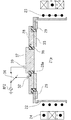
図1は、本発明の実施形態によるプラズマ処理装置20の概略構成を示す側断面図である。本実施形態では、エッチング処理と側壁保護膜の形成を交互に行うことによって、Si基板の表面に高アスペクト比の孔又は溝を形成するプラズマ処理装置に本発明を適用した例について説明する。
FIG. 1 is a side sectional view showing a schematic configuration of a
図1において、21は真空槽であり、内部に反応室21aを形成している。真空槽21には例えばターボ分子ポンプ等の真空ポンプ27が接続され、真空槽21の内部が所定の真空度に真空排気されている。
In FIG. 1,
反応室21aの周囲を構成する筒状容器22は石英等の透明材料からなり、その外周側には、第1の高周波電源RF1に接続されたプラズマ発生用の高周波コイル23と、この高周波コイル23の外周側に3つの磁気コイル24A,24B,24Cからなる磁気コイル群24がそれぞれ配置されている。ここで、高周波コイル23は、本発明の「第1のプラズマ源」に対応し、磁気コイル群24は、本発明の「磁場形成手段」に対応する。
The
磁気コイル24Aと磁気コイル24Cにはそれぞれ同一方向の電流が供給され、磁気コイル24Bには他の磁気コイル24A,24Cと逆方向に電流が供給される。その結果、反応室21aにおいて、磁場ゼロの環状の磁気中性線25が形成され、高周波コイル23により磁気中性線25に沿って誘導電場が印加されることで、反応室21aに放電プラズマが形成される。
A current in the same direction is supplied to the
反応室21aには、基板30を支持するステージ26が設置されている。ステージ26は金属製で、コンデンサ31を介してバイアス電源としての第4の高周波電源RF4に接続されている。ステージ26に第4の高周波電源RF4を接続することで、基板バイアスによりイオンをステージ26側に加速させ、基板30上のラジカル生成物をスパッタ除去してエッチング性を高めることができる。
A
筒状容器22の上部には、反応室21aへプロセスガスを導入するガス導入ノズル29が設置されている。プロセスガスとしては、Ar、He等の希ガスとエッチングガスが用いられる。エッチングガスとしては、エッチング対象物によって適宜選択され、例えばSi系の材料をエッチングする場合には、SF系、CF系、CHF系などのハロゲン系ガス又はこれと希ガスとの混合ガスが用いられる。
A
また、筒状容器22の上部は天板28で閉塞されている。天板28は金属製で、ステージ26の対向電極として構成されている。この天板28には、コンデンサ32を介してバイアス電源としての第3の高周波電源RF3が接続されている。高周波電源RF3は、エッチング領域の正イオンによるチャージアップを抑制し、高アスペクト比のエッチング加工を実現する。
The upper part of the
天板28は、中央部に開口28aを有している。この開口28aには、誘電体からなる窓部材33が設置されている。窓部材33は、例えば石英、透光性セラミックス等の透明材料で形成されている。そして、この窓部材33には、第2の高周波電源RF2に接続されたプラズマ発生用のループ状のRFアンテナ34が設置されている。RFアンテナ34は、反応室21aに発生したプラズマの密度分布を調整するための第2のプラズマ源を構成する。
The
本実施形態では、RFアンテナ34のループ径は、磁気コイル群24によって形成される環状磁気中性線25の直径よりも小さくなるように設定されているとともに、RFアンテナ34のループ中心が磁気中性線25の中心とほぼ一致するように窓部材33に設置されている。RFアンテナ34のループ径は適宜選択され、磁気中性線25の径内方領域において所望のプラズマ分布が得られる大きさに設定される。
In the present embodiment, the loop diameter of the
窓部材33の上方には、ステージ26上の基板30の被処理面を検出するセンサ41が設置されている。このセンサ41は、CCD等の固体撮像素子やフォトカプラー等の光学式検出器で構成される。窓部材33をセンサ41の検出窓として用いることで、基板を横方向からモニタする場合と異なり、基板30のエッチング深さをリアルタイムで検出することが可能となる。例えば、基板表面のレジスト膜を全面除去したい場合に、面内でどのようにレジスト膜が除去されていくかがリアルタイムで確認できるようになる。
Above the
天板28の反応室21aと対向する側の面には、スパッタ用のターゲット35が設置されている。ターゲット35は、反応室21aに形成されたプラズマ中のイオンによりスパッタされ、そのスパッタ物は、ステージ26上の基板30の表面に堆積される。本実施形態では、ターゲット35の構成材料として合成樹脂材料、例えばポリテトラフルオロエチレン(PTFE)が用いられている。なお、ターゲット35の構成材料は合成樹脂材料に限られず、金属、シリコン、セラミックス等の単質材又はこれらの複合材を用いることが可能である。
A
以上のように構成される本実施形態のプラズマ処理装置20においては、反応室21aにエッチングガスのプラズマを発生させることで、ステージ26上の基板30の表面をエッチングする。基板30の表面には予め所定形状のレジストパターンが形成されており、当該レジストパターンの開口部においてエッチングが進行する。一方、反応室21aに希ガスのプラズマを発生させることで、天板28に設置したターゲット35をスパッタし、そのスパッタ物を基板30の表面及びエッチングパターンの底部及び側壁部に付着させる。これらエッチング処理およびスパッタ処理を交互に行うことによって、基板30の表面に高アスペクト比の孔又は溝を高精度に形成することが可能となる。
In the
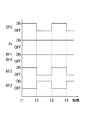
図2は、エッチングガス、希ガスの導入タイミングと高周波電源RF1〜RF4の印加タイミングとの関係を示すタイミングチャートである。本例では、エッチングガスとしてSF6ガスが用いられ、希ガスとしてArガスが用いられている。 FIG. 2 is a timing chart showing the relationship between the introduction timing of the etching gas and the rare gas and the application timing of the high frequency power sources RF1 to RF4. In this example, SF 6 gas is used as the etching gas, and Ar gas is used as the rare gas.
RF1及びRF4は高周波アンテナ23及びステージ26に常に印加されている。高周波アンテナ23への電力供給時は磁気コイル群24に対しても所定の電力供給が行われる。したがって、反応室26aには、磁気中性線25に沿って高密度なプラズマが形成されるとともに、プラズマ中のイオンがステージ26側へ周期的に引き込まれる。
RF1 and RF4 are always applied to the high-
基板30のエッチング処理時(時間t1〜t2)、反応室21aにエッチングガス(SF6)が導入され、当該エッチングガスのプラズマが形成される。このときの反応室21aの圧力は、例えば2Pa〜10Paに設定される。このような比較的高圧の減圧雰囲気下では、磁気コイル群24に対する電流供給制御を行ってもプラズマ分布の調整は不可能である。そこで、第2のプラズマ源であるRFアンテナ34へ高周波電源RF2を印加することにより、磁気中性線25の径内方位置におけるプラズマ密度が高められるようにプラズマ分布が調整される。これにより、基板30の面内におけるエッチング速度の均一性が高められる。
During the etching process of the substrate 30 (time t1 to t2), an etching gas (SF 6 ) is introduced into the
本実施形態によれば、第2のプラズマ源であるRFアンテナ34を天板28の所定領域に限って設置するようにしているので、当該第2のプラズマ源によって形成される電場領域を磁気中性線25の所望の径内方領域に限定でき、当該領域のプラズマ密度を高めることが可能となる。
According to the present embodiment, since the
また、窓部材33にRFアンテナ34が設置されることによって、窓部材33への膜の付着を抑えられ、これにより窓部材33の透光性を安定に維持し、センサ41を用いたエッチングプロセスの連続モニタを行うことが可能となる。
Further, since the
一方、側壁保護膜の形成時(時間t2〜t3)においては、エッチングガスの導入は停止され、希ガスのみのプラズマが形成される。また、RFアンテナ34に対する高周波電源RF2の投入が停止され、代わりに、天板28に対してバイアス電源RF3が印加される。バイアス電源RF3の印加により、天板28に対するプラズマ中のイオンのスパッタ作用が得られる。これにより、天板28に付着したエッチングガスの反応生成物が除去されると同時に、ターゲット35がスパッタされてそのスパッタ物が基板30のエッチングパターンの底部および側壁部に付着し保護膜を形成する。
On the other hand, at the time of forming the sidewall protective film (time t2 to t3), the introduction of the etching gas is stopped, and plasma of only a rare gas is formed. In addition, the high frequency power supply RF2 is turned off to the
この側壁保護膜の形成工程では、反応室21aの圧力が例えば0.1Pa〜1.5Paに設定される。このような比較的低圧の減圧雰囲気下では、磁気コイル群24に対する電流制御のみによって磁気中性線25の形成領域の調整すなわちプラズマ分布の調整が可能となる。具体的には、磁気コイル24A,24B,24Cに供給する電流をそれぞれIA,IB,ICとしたとき、IA>ICの場合は磁気中性線25の形成位置は磁気コイル24C側へ下がり、逆に、IA<ICの場合は磁気中性線25の形成位置は磁気コイル14A側へ上がる。また、中間の磁気コイル24Bに供給する電流IBを増していくと、磁気中性線25のリング径は小さくなると同時に、磁場ゼロの位置での磁場の勾配が緩やかになる。従って、これらの特性を利用することで、プラズマ密度分布の最適化を図ることが可能となり、基板30の面内に対する保護膜の成膜速度の均一性が高められる。
In the side wall protective film forming step, the pressure in the
保護膜の形成が所定時間行われた後、再び、反応室21aへエッチングガスが導入され、上述したのと同様なエッチング処理が再び行われる。このとき、エッチング初期段階において、基板30の表面およびエッチングパターンの底部に形成された保護膜は、プラズマ中のイオンのスパッタ作用により除去される。当該イオンは基板に対してほぼ垂直に入射するため、エッチングパターンの側壁部に付着した保護膜は完全に除去されることなく残留する。
After the protective film is formed for a predetermined time, the etching gas is again introduced into the
以上のようにして、基板30の表面に対して高アスペクト比の深掘り加工が行われる。本実施形態によれば、エッチング処理時は第2のプラズマ源を用いてプラズマ分布を調整することでエッチングレートの面内均一性を高めるようにし、また、保護膜成膜時は磁気コイル群24に対する電流制御でプラズマ分布を調整することで成膜レートの面内均一性を高めるようにしているので、基板30の面内において高精度な深掘り加工を実現することが可能となる。
As described above, deep digging with a high aspect ratio is performed on the surface of the
図3は、第2のプラズマ源(RFアンテナ34)の設置の有無によるエッチング速度の面内(X−Y方向)均一性を示す一実験結果である。実験条件は以下のとおりである。
[実験条件]
・RF1:13.56MHz、3kW
・RF2:12.5MHz、0.5kW
・RF3:12.5MHz、0.5kW
・エッチングガス:SF6+Ar
・エッチング圧力:10Pa
・基板サイズ:8インチ
FIG. 3 shows one experimental result showing in-plane (XY direction) uniformity of the etching rate depending on whether or not the second plasma source (RF antenna 34) is installed. The experimental conditions are as follows.
[Experimental conditions]
・ RF1: 13.56MHz, 3kW
・ RF2: 12.5MHz, 0.5kW
・ RF3: 12.5MHz, 0.5kW
Etching gas: SF 6 + Ar
・ Etching pressure: 10Pa
・ Board size: 8 inches
図3の結果から明らかなように、第2のプラズマ源が無い場合、基板の外周側でエッチング速度が高い。これは、磁気中性線の形成位置に対応したプラズマ分布が生じていることを示している。これに対し、第2のプラズマ源を設置することで、エッチング速度の面内均一性が改善されることがわかる。これは、第2のプラズマ源の設置により、磁気中性線の径内方側(基板中央側)において電場の形成密度が高められ、その結果、基板外周部のエッチング速度が低下し、かつ基板中心部のエッチング速度が高められたことに起因する。 As is apparent from the results of FIG. 3, when there is no second plasma source, the etching rate is high on the outer peripheral side of the substrate. This indicates that a plasma distribution corresponding to the formation position of the magnetic neutral line is generated. On the other hand, it can be seen that the in-plane uniformity of the etching rate is improved by installing the second plasma source. This is because the formation density of the electric field is increased on the radially inner side (substrate central side) of the magnetic neutral wire by the installation of the second plasma source, and as a result, the etching rate of the outer peripheral portion of the substrate is reduced, and the substrate This is because the etching rate at the center is increased.
図4は、本発明の他の実施形態によるプラズマ処理装置の要部の概略構成図である。図示するプラズマ処理装置は、RFアンテナ(第2のプラズマ源)34の高周波電源RF2を天板28のバイアス電源に兼用した構成を備えている。この場合、高周波電源RF2と天板28(コンデンサ32)及びRFアンテナ34との間に、切替手段としてのスイッチ36が接続される。スイッチ36は、高周波電源RF2に対する天板28及びRFアンテナ34の接続を選択的に切り替える機能を有する。
FIG. 4 is a schematic configuration diagram of a main part of a plasma processing apparatus according to another embodiment of the present invention. The illustrated plasma processing apparatus has a configuration in which the high frequency power source RF2 of the RF antenna (second plasma source) 34 is also used as the bias power source of the
以上の構成により、スイッチ36による切替操作でRFアンテナ34に対する電力投入と天板28に対する電力投入を選択的に切り替えることが可能となるので、エッチング処理と成膜処理を交互に行うプラズマ処理装置において、電力の切替えを容易かつ的確に行うことが可能となる。また、電力設置コストの低減と制御回路の簡素化を図ることが可能となる。
With the above configuration, it is possible to selectively switch between the power input to the
図5は、本発明の更に他の実施形態によるプラズマ処理装置の要部の概略構成図である。図示するプラズマ処理装置は、第2のプラズマ源をRFアンテナに代えて、RF電極37で構成した例を示している。RF電極37は金属製で、誘電体38を介して天板28の開口28a内に設置されているとともに、コンデンサ39及びスイッチ36を介して高周波電源RF2に接続されている。なお、高周波電源RF2は、RF電極37及び天板28に対して共通とする場合に限られず、RF電極37に対して専用の高周波電源で構成されていても構わない。
FIG. 5 is a schematic configuration diagram of a main part of a plasma processing apparatus according to still another embodiment of the present invention. The illustrated plasma processing apparatus shows an example in which the second plasma source is configured by an
本実施形態のプラズマ処理装置は、図1に示したようにRFアンテナ34による誘導結合(ICP)方式のプラズマ源を構成する例に代えて、ステージ26を対向電極とする容量結合(CCP)方式のプラズマ源を構成している。この例によっても、反応室21aにおいて形成されるプラズマの密度分布の調整を行うことが可能であり、エッチングレートの面内均一性の向上を図れるようになる。
As shown in FIG. 1, the plasma processing apparatus according to the present embodiment replaces an example in which an inductively coupled (ICP) type plasma source with an
以上、本発明の実施形態について説明したが、勿論、本発明はこれに限定されることはなく、本発明の技術的思想に基づいて種々の変形が可能である。 As mentioned above, although embodiment of this invention was described, of course, this invention is not limited to this, A various deformation | transformation is possible based on the technical idea of this invention.
例えば以上の実施形態では、基板に対してエッチング処理と成膜処理を交互に施して高アスペクト比の孔又は溝を形成するプラズマ処理装置を例に挙げて説明したが、勿論、基板のエッチング処理に特化したプラズマエッチング装置にも本発明は適用可能である。 For example, in the above embodiment, the plasma processing apparatus that forms the high aspect ratio hole or groove by alternately performing the etching process and the film forming process on the substrate has been described as an example. The present invention can also be applied to a plasma etching apparatus specialized for the above.
20 プラズマ処理装置
21 真空槽
23 高周波コイル(第1のプラズマ源)
24 磁気コイル群(磁場形成手段)
25 磁気中性線
26 ステージ
27 真空ポンプ
28 天板
29 ガス導入ノズル(ガス導入手段)
30 基板
33 窓部材(誘電体)
34 RFアンテナ(第2のプラズマ源)
35 ターゲット
36 スイッチ(切替手段)
37 RF電極(第2のプラズマ源)
38 誘電体
41 センサ
RF1 第1の高周波電源
RF2 第2の高周波電源
RF3,RF4 バイアス電源
20
24 Magnetic coil group (magnetic field forming means)
25 Magnetic
30
34 RF antenna (second plasma source)
35
37 RF electrode (second plasma source)
38
Claims (7)
中央部に開口を有し、前記開口に誘電体が設置された、前記真空槽の上部を閉塞する天板と、
前記反応室の周囲に配置され第1の高周波電源に接続された第1のプラズマ源と、
前記反応室に設置され所定のバイアス電源に接続された基板支持用のステージと、
前記反応室へプロセスガスを導入するガス導入手段と、
前記反応室に磁場ゼロの環状磁気中性線を形成する磁場形成手段と、
前記開口に前記誘電体を介して設置され、第2の高周波電源に接続された、前記磁気中性線の径内方位置におけるプラズマ密度が高められるようにプラズマ分布を調整可能な第2のプラズマ源と、
を備えたプラズマ処理装置。 A vacuum chamber forming a reaction chamber;
A top plate that has an opening in the center, and a dielectric is installed in the opening, closing the upper part of the vacuum chamber;
A first plasma source disposed around the reaction chamber and connected to a first high frequency power source;
A stage for supporting a substrate installed in the reaction chamber and connected to a predetermined bias power source;
Gas introduction means for introducing process gas into the reaction chamber;
A magnetic field forming means for forming an annular magnetic neutral line having no magnetic field in the reaction chamber ;
A second plasma that is installed in the opening via the dielectric and is connected to a second high-frequency power source and capable of adjusting the plasma distribution so that the plasma density at the radially inner position of the magnetic neutral wire is increased. The source ,
A plasma processing apparatus comprising:
請求項1に記載のプラズマ処理装置。 The plasma processing apparatus according to claim 1 , wherein the dielectric is made of a transparent material, and the second plasma source is an RF antenna.
請求項2に記載のプラズマ処理装置。 The plasma processing apparatus of Claim 2. The sensor which optically monitors the to-be-processed surface of the board | substrate inside a vacuum chamber through the said dielectric material.
請求項1に記載のプラズマ処理装置。 The plasma processing apparatus according to claim 1, wherein the second plasma source is an RF electrode.
請求項1に記載のプラズマ処理装置。 The plasma processing apparatus according to claim 1, wherein the top plate is connected to a third high-frequency power source different from the second high-frequency power source.
請求項1に記載のプラズマ処理装置。 The top plate and the second plasma source are connected to the second high-frequency power source via a switching unit, and the switching unit includes the top plate and the second plasma for the second high-frequency power source. The plasma processing apparatus according to claim 1, wherein the source connection is selectively switched.
請求項1に記載のプラズマ処理装置。 The plasma processing apparatus according to claim 1, wherein a sputtering target is installed on a surface of the top plate that faces the reaction chamber.
Priority Applications (1)
| Application Number | Priority Date | Filing Date | Title |
|---|---|---|---|
| JP2007078860A JP5065725B2 (en) | 2007-03-26 | 2007-03-26 | Plasma processing equipment |
Applications Claiming Priority (1)
| Application Number | Priority Date | Filing Date | Title |
|---|---|---|---|
| JP2007078860A JP5065725B2 (en) | 2007-03-26 | 2007-03-26 | Plasma processing equipment |
Publications (2)
| Publication Number | Publication Date |
|---|---|
| JP2008243917A JP2008243917A (en) | 2008-10-09 |
| JP5065725B2 true JP5065725B2 (en) | 2012-11-07 |
Family
ID=39914937
Family Applications (1)
| Application Number | Title | Priority Date | Filing Date |
|---|---|---|---|
| JP2007078860A Active JP5065725B2 (en) | 2007-03-26 | 2007-03-26 | Plasma processing equipment |
Country Status (1)
| Country | Link |
|---|---|
| JP (1) | JP5065725B2 (en) |
Families Citing this family (6)
| Publication number | Priority date | Publication date | Assignee | Title |
|---|---|---|---|---|
| JP2012142317A (en) * | 2010-12-28 | 2012-07-26 | Ulvac Japan Ltd | Etching apparatus and etching method |
| JP5727853B2 (en) * | 2011-04-28 | 2015-06-03 | 株式会社アルバック | Plasma generation method |
| KR101794088B1 (en) * | 2012-04-03 | 2017-11-07 | 주식회사 원익아이피에스 | plasma processing apparatus, and substrate processing method |
| KR101649947B1 (en) * | 2014-07-08 | 2016-08-23 | 피에스케이 주식회사 | Apparatus for generating plasma using dual plasma source and apparatus for treating substrate comprising the same |
| CN107369602B (en) * | 2016-05-12 | 2019-02-19 | 北京北方华创微电子装备有限公司 | Reaction chamber and semiconductor processing equipment |
| CN110416053B (en) | 2019-07-30 | 2021-03-16 | 江苏鲁汶仪器有限公司 | Inductively coupled plasma processing system |
Family Cites Families (9)
| Publication number | Priority date | Publication date | Assignee | Title |
|---|---|---|---|---|
| JPH0773997A (en) * | 1993-06-30 | 1995-03-17 | Kobe Steel Ltd | Plasma cvd device and cvd processing method employing the device and cleaning method for inside of the device |
| JPH07263192A (en) * | 1994-03-24 | 1995-10-13 | Ulvac Japan Ltd | Etching device |
| JPH09270416A (en) * | 1996-03-29 | 1997-10-14 | Sony Corp | Dry etching device and dry etching method |
| JP3955351B2 (en) * | 1996-12-27 | 2007-08-08 | キヤノンアネルバ株式会社 | Plasma processing equipment |
| JP3940464B2 (en) * | 1997-05-14 | 2007-07-04 | 株式会社アルバック | Reactive ion etching apparatus and method |
| JP3676919B2 (en) * | 1997-10-09 | 2005-07-27 | 株式会社アルバック | Reactive ion etching system |
| JP4474026B2 (en) * | 2000-07-13 | 2010-06-02 | アルバック成膜株式会社 | Method for controlling spatial distribution of inductively coupled plasma, and plasma generating apparatus and etching apparatus for implementing the method |
| JP4171590B2 (en) * | 2001-05-18 | 2008-10-22 | 株式会社アルバック | Etching method |
| JP4796965B2 (en) * | 2004-07-02 | 2011-10-19 | 株式会社アルバック | Etching method and apparatus |
-
2007
- 2007-03-26 JP JP2007078860A patent/JP5065725B2/en active Active
Also Published As
| Publication number | Publication date |
|---|---|
| JP2008243917A (en) | 2008-10-09 |
Similar Documents
| Publication | Publication Date | Title |
|---|---|---|
| JP5207406B2 (en) | Plasma processing method | |
| JP2022183200A (en) | Control method, plasma processing device, processor, and non-transitory computer-readable recording medium | |
| EP1573795B1 (en) | A system and method for controlling plasma with an adjustable coupling to ground circuit | |
| JP5808697B2 (en) | Dry etching apparatus and dry etching method | |
| KR101061673B1 (en) | Plasma processing apparatus, plasma processing method and storage medium | |
| JP7345382B2 (en) | Plasma processing equipment and control method | |
| US20090308732A1 (en) | Apparatus and method for uniform deposition | |
| JP5065725B2 (en) | Plasma processing equipment | |
| KR100552641B1 (en) | Plasma processing apparatus and plasma processing method | |
| JP7236477B2 (en) | PVD equipment | |
| JP2012038461A (en) | Plasma processing apparatus | |
| US20130299091A1 (en) | Plasma processing apparatus | |
| JP2012142495A (en) | Plasma etching method and plasma etching apparatus | |
| JP2002217171A (en) | Etching equipment | |
| KR101189847B1 (en) | Plasma processing method | |
| KR20160071321A (en) | Plasma etching method | |
| JP2006100485A (en) | Branch switch for high frequency power and etching apparatus | |
| KR100455350B1 (en) | Device for prducing inductively coupled plasma and method | |
| KR101871900B1 (en) | High frequency sputtering apparatus and sputtering method | |
| JP5072066B2 (en) | Plasma forming method | |
| JP4171590B2 (en) | Etching method | |
| JPS6350025A (en) | Production apparatus for semiconductor | |
| KR20160071452A (en) | Insulating material target | |
| JP2010168663A (en) | Plasma treatment apparatus | |
| JPH10163058A (en) | Device for manufacturing magnetic thin film |
Legal Events
| Date | Code | Title | Description |
|---|---|---|---|
| A621 | Written request for application examination |
Free format text: JAPANESE INTERMEDIATE CODE: A621 Effective date: 20100122 |
|
| A977 | Report on retrieval |
Free format text: JAPANESE INTERMEDIATE CODE: A971007 Effective date: 20110704 |
|
| A131 | Notification of reasons for refusal |
Free format text: JAPANESE INTERMEDIATE CODE: A131 Effective date: 20120515 |
|
| A521 | Request for written amendment filed |
Free format text: JAPANESE INTERMEDIATE CODE: A523 Effective date: 20120717 |
|
| TRDD | Decision of grant or rejection written | ||
| A01 | Written decision to grant a patent or to grant a registration (utility model) |
Free format text: JAPANESE INTERMEDIATE CODE: A01 Effective date: 20120807 |
|
| A01 | Written decision to grant a patent or to grant a registration (utility model) |
Free format text: JAPANESE INTERMEDIATE CODE: A01 |
|
| A61 | First payment of annual fees (during grant procedure) |
Free format text: JAPANESE INTERMEDIATE CODE: A61 Effective date: 20120810 |
|
| R150 | Certificate of patent or registration of utility model |
Ref document number: 5065725 Country of ref document: JP Free format text: JAPANESE INTERMEDIATE CODE: R150 Free format text: JAPANESE INTERMEDIATE CODE: R150 |
|
| FPAY | Renewal fee payment (event date is renewal date of database) |
Free format text: PAYMENT UNTIL: 20150817 Year of fee payment: 3 |
|
| R250 | Receipt of annual fees |
Free format text: JAPANESE INTERMEDIATE CODE: R250 |
|
| R250 | Receipt of annual fees |
Free format text: JAPANESE INTERMEDIATE CODE: R250 |
|
| R250 | Receipt of annual fees |
Free format text: JAPANESE INTERMEDIATE CODE: R250 |
|
| R250 | Receipt of annual fees |
Free format text: JAPANESE INTERMEDIATE CODE: R250 |
|
| R250 | Receipt of annual fees |
Free format text: JAPANESE INTERMEDIATE CODE: R250 |
|
| R250 | Receipt of annual fees |
Free format text: JAPANESE INTERMEDIATE CODE: R250 |
|
| R250 | Receipt of annual fees |
Free format text: JAPANESE INTERMEDIATE CODE: R250 |