JP5056552B2 - Electronic device mounting structure - Google Patents
Electronic device mounting structure Download PDFInfo
- Publication number
- JP5056552B2 JP5056552B2 JP2008100268A JP2008100268A JP5056552B2 JP 5056552 B2 JP5056552 B2 JP 5056552B2 JP 2008100268 A JP2008100268 A JP 2008100268A JP 2008100268 A JP2008100268 A JP 2008100268A JP 5056552 B2 JP5056552 B2 JP 5056552B2
- Authority
- JP
- Japan
- Prior art keywords
- electronic device
- substrate
- moisture
- mounting structure
- lead
- Prior art date
- Legal status (The legal status is an assumption and is not a legal conclusion. Google has not performed a legal analysis and makes no representation as to the accuracy of the status listed.)
- Expired - Fee Related
Links
Images


Landscapes
- Structures Or Materials For Encapsulating Or Coating Semiconductor Devices Or Solid State Devices (AREA)
Description
本発明は基板上に半田付けされた電子装置のリードに防湿剤を塗布する構成の電子装置の実装構造に関する。 The present invention relates to a mounting structure for an electronic device having a structure in which a moisture-proofing agent is applied to leads of the electronic device soldered onto a substrate.
QFN(Quad Flat Non-Leaded Package)構造の電子装置(半導体パッケージ)の実装構造は、特許文献1により知られている。
このQFN構造の電子装置に似た四方向リードタイプのパッケージ構造にQFP(Quad Flat Package)構造の電子装置がある。このQFP構造の電子装置では、QFN構造のものとは異なり、多数のリードが四側面から外方に突出する構造である。このQFP構造の電子装置では、車両に搭載される機器などに用いられる場合、使用環境の温度変化によってリードに結露し、結露水によってリード間が短絡されるといった事故を起す恐れがあるので、これを避けるために、基板に半田付けした後、リード部分を覆うようにヒューミシール(エアブラウン社の商標)などの防湿剤を塗布するようにしている。
There is an electronic device having a QFP (Quad Flat Package) structure as a four-way lead type package structure similar to the electronic device having the QFN structure. Unlike the QFN structure, the electronic device having the QFP structure has a structure in which a large number of leads protrude outward from the four side surfaces. In this electronic device with QFP structure, when used in equipment mounted on a vehicle, there is a risk that condensation will occur on the leads due to temperature changes in the environment of use and there will be a short circuit between the leads due to condensed water. In order to avoid this, after soldering to the substrate, a moisture-proofing agent such as Humiseal (trademark of Air Brown) is applied so as to cover the lead portion.
一般にこれらの防湿剤は塗布時に、液状で流動性が高いことが知られている。このため、電子装置のリード部分に防湿剤を塗布する際に、防湿剤が基板と電子装置との間の小さな隙間内にも浸入し硬化する。硬化した防湿剤は、周囲の温度変化に伴って膨張収縮し、膨張時には基板に対して電子装置に押し上げの力を発生させ、収縮時には基板に対して電子装置を引っ張る押し下げの力を発生させるため、リードの半田付け部分が応力を受ける。そして、長期の使用では電子装置のリードの半田が防湿剤の膨張収縮に伴い繰り返し応力を受けて疲労するという恐れがある。ただし、リード部を覆うように塗布されている防湿剤の熱膨張による応力はリード線の回りから均等にかかるため、半田付け部の疲労にはほとんど関与しないと考えられ、特に問題になるのは電子装置と基板部の隙間に浸入した防湿剤である。 In general, it is known that these moisture-proofing agents are liquid and have high fluidity when applied. For this reason, when the moisture-proofing agent is applied to the lead portion of the electronic device, the moisture-proofing agent also enters and cures in a small gap between the substrate and the electronic device. The cured moisture-proof agent expands and contracts as the ambient temperature changes, and when it expands, it generates a pushing force on the electronic device against the substrate, and when it shrinks it generates a pushing force that pulls the electronic device against the substrate. The soldered part of the lead is subjected to stress. In long-term use, the solder of the lead of the electronic device may be fatigued due to repeated stress accompanying expansion and contraction of the moisture-proof agent. However, since the stress due to thermal expansion of the moisture-proofing agent applied so as to cover the lead part is applied evenly from around the lead wire, it is considered that it hardly affects the fatigue of the soldered part, and it is particularly problematic It is a moisture-proofing agent that has entered the gap between the electronic device and the substrate.
本発明は上記の事情に鑑みてなされたもので、その目的は、半田付け部分に繰り返し応力が作用することを極力防止できる電子装置の実装構造を提供することにある。 The present invention has been made in view of the above circumstances, and an object of the present invention is to provide an electronic device mounting structure capable of preventing stress from being repeatedly applied to a soldered portion as much as possible.
請求項1の発明では、防湿剤が基板と電子装置の間に浸入しない構造を提案する。また、基板に、電子装置方向に開口部を持つ溝を形成することを特徴としている。これにより、電子装置と基板の間の隙間に浸入しようとした防湿剤はこの溝内に貯留され、隙間内に浸入することを抑制する。請求項2の発明では、上記の防湿剤浸入防止構造が、電子装置のリードよりも内側に設置されているものを規定している。請求項3の発明では、溝の代わりに裏面にまで到達する貫通孔を設けることで、同様の効果を企図したものである。
請求項4は具体的な例で、電子装置の基板に向き合った面にダム状の突出した形状の土手を形成したものである。この形状のダム的な効果によって防湿剤が基板と電子装置との間の隙間内に浸入することが防止される。これにより防湿剤の温度変化による膨張収縮に関する影響は排除できる。また、請求項5は、その突出形状を電子装置の側面に則して設けたものであり、これにより隙間内に浸入する防湿剤を最小限に抑える効果がある請求項6の発明では、電子装置が基板に実装されたときには突出部が接触しないような寸法とすることが規定されている。こうすることによって実装の半田付け時にリードが浮くことによる半田付け不良を防止することができる。
The invention of claim 1 proposes a structure in which the moisture-proofing agent does not enter between the substrate and the electronic device. In addition, a groove having an opening in the direction of the electronic device is formed in the substrate. As a result, the desiccant that is about to enter the gap between the electronic device and the substrate is stored in the groove, and is prevented from entering the gap. In the invention of
請求項7の発明では、防湿剤が浸入する防壁を基板側に設けた構造を提案したものである。
The invention of
請求項8の発明では、上記の防湿剤浸入防止構造が、電子装置のリードよりも内側に設置されているものを規定している。熱膨張による半田疲労に関与する防湿剤はリード線よりも内側に浸入したものが主な原因となるため、それを抑制することを目的としている。
In the invention of
以下、本発明を、自動車に搭載されるヨーレートセンサに適用して実施形態により具体的に説明する。なお、ヨーレートセンサは、自動車の回転角速度(ヨーレート)を検出するためのもので、センサ素子が検出した回転角速度をデジタル信号にして出力するものである。 Hereinafter, the present invention will be described in detail with reference to embodiments by applying it to a yaw rate sensor mounted on an automobile. The yaw rate sensor is for detecting the rotational angular velocity (yaw rate) of the automobile, and outputs the rotational angular velocity detected by the sensor element as a digital signal.
[第1の実施形態]
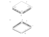
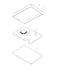
図1〜図3は本発明の第1の実施形態を示す。ヨーレートセンサ1は、分解して示す図3のように、開放された一面を蓋板2によって塞がれるケース3内に、複数の電気・電子部品を搭載したプリント配線基板(基板)4を収納して構成される。プリント配線基板4上の電気・電子部品には、角速度を検出するセンサ素子5、センサ素子5から出力されるアナログ信号を処理してデジタル信号化する演算素子(電子装置)6などが含まれる。なお、図3には、センサ素子4および演算素子6以外の他の電気電子部品は図示されていない。
[First Embodiment]
1 to 3 show a first embodiment of the present invention. The yaw rate sensor 1 houses a printed wiring board (board) 4 on which a plurality of electric / electronic components are mounted in a case 3 whose one open surface is closed by a
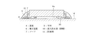
演算素子6は、半導体チップとリードフレームとをモールド樹脂により封止してなるもので、図2に示すように、矩形状をなし、その四側面から多数のリード7が取り出されたQFP構造を有する。この演算素子6は表面実装型で、そのリード7は、図1に示すように、プリント配線基板(基板)4の表面に形成された多数のランド8に半田9付けによって電気的に接続されると共に機械的に固定される。
The
この演算素子6の厚さ方向の両面のうち、プリント配線基板4に搭載されたときに当該プリント配線基板4と対向する面(基板側端面、以下、裏面という。)6aには、外周に沿って突出した構造である凸条(浸入防止部)10が設けられている。この凸条10は、ICチップを樹脂封止する際の型成形により、封止用のモールド樹脂と一体に矩形枠状に形成されたものである。
Of both surfaces of the
本実施形態の場合、凸条10は、演算素子6のプリント配線基板4に略垂直に沿った側面(前後左右の側面)から延設されると共に、演算素子6の裏面6aを囲みプリント配線基板4方向に突出する囲壁となっており、この凸条10によって囲まれた領域は中空となっている。また、この凸条10の裏面6aからの突出量、つまり高さ寸法hは、リード7の裏面6aからの突出寸法H(プリント配線基板4のリード7の半田付け部分であるランド8と演算素子6の裏面6aとの間の距離に相当)よりもやや小さくなっている。
In the case of this embodiment, the
上記の演算素子6をプリント配線基板4に実装するには、まず、演算素子6の各リード7をプリント配線基板4の各ランド8上に載置し、各リード7を各ランド8に半田付けする。この状態では、各リード7とプリント配線基板4との接点、つまり半田9付けされた部分は、全て囲壁である凸条10の外側に位置している。半田付け後、演算素子6をプリント配線基板4に半田付けし、そして、リード7には防湿剤11を塗布する。この防湿剤11は、流動性を有した粘液状のもので、固化すると、硬質なものとなる。
In order to mount the
この防湿剤11は、リード7、ランド8、リード7をランド8に接続した半田9を、これらの全体を覆うような状態で塗布される。この際、防湿剤11は、演算素子6とプリント配線基板4との間の隙間内に浸入しようとするが、演算素子6の裏面6aに凸条10が突設されていて、この凸条10とプリント配線基板4との間の隙間が極く狭くなっているので、防湿剤11が凸条10によって演算素子6とプリント配線基板4との間の隙間内に浸入することが阻止される。
The moisture-
このように本実施形態によれば、防湿剤11がリード7、ランド8、半田9を覆っているので、周囲温度の変化によって結露が生じても、リード7同士が結露などによる水分によって電気的に接続された状態(短絡)になる恐れがない。その上、防湿剤11が演算素子6とプリント配線基板4との間の隙間内に浸入することが凸条10によって極力防止されるので、温度変化によって防湿剤11が膨張収縮しても、演算素子6が持ち上げられたりする恐れがない。それは、リードの回りを覆う防湿剤11の熱膨張による力はリード7とランド8に対して周りから均等にかかるため、半田疲労を誘発する応力とはなりにくく、問題となるのは隙間内に浸入した防湿剤であるためである。このため、半田9が防湿剤11の膨張収縮の影響を受ける恐れが本来的になくなり、半田9が繰り返し応力を受けて早期に疲労するという事態の発生を極力防止することができる。
As described above, according to the present embodiment, since the moisture-
[第2の実施形態]
図4および図5は本発明の第2の実施形態を示すものである。この実施形態は、上記第1の実施形態の演算素子6に凸条10を設けることに代えて、プリント配線基板4上に矩形枠状の凸条12を設けたところにある。プリント配線基板4上の凸条12は、インクをシルク印刷により盛り上げることによって形成したものである。
[Second Embodiment]
4 and 5 show a second embodiment of the present invention. In this embodiment, instead of providing the
この実施形態においても、第1の実施形態と同様に、凸条12は囲壁を構成し、この凸条12によって囲まれた領域は中空になっていると共に、各リード7とプリント配線基板4との接点、つまり半田9付けされた部分は、全て凸条12の外側に位置している。また、凸条12のプリント配線基板4からの突出量(高さ)は、リード7の裏面6aからの突出寸法よりもやや小さくなっている。
Also in this embodiment, as in the first embodiment, the
このようにプリント配線基板4側に、プリント配線基板4と演算素子6との間に防湿剤11が侵入することを防止する凸条12を設けた場合であっても、前述の第1実施形態と同様の効果を奏することができる。
さらに、本実施形態2のように、シルク印刷により凸条12を形成すれば、演算素子6の載置前にシルク印刷を行うだけで済むため、特段に工程を複雑化させることなく、上記効果を奏することができる。
As described above, even when the
Furthermore, if the
[第3の実施形態]
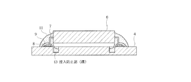
図6は本発明の第3の実施形態を示すものである。この実施形態は、上記第2の実施形態の凸条12を設けることに代えて、プリント配線基板4上に演算素子6方向に向けて開口する溝(浸入防止部)13を設けたところにある。この溝13は、演算素子6によって覆われた領域に、その全周にわたって形成されている。そして、この溝13の外側に各リード7とプリント配線基板4との接点である半田9付け部分が位置している。
[Third Embodiment]
FIG. 6 shows a third embodiment of the present invention. In this embodiment, instead of providing the
このようにプリント配線基板4側に溝13を設けた場合には、余分の防湿剤11は溝13内に浸入しそこに溜められてプリント配線基板4と演算素子6との間に浸入することが防止されるので、前述の各実施形態と同様の効果を奏することができる。
更に、このような溝13を設ければ、防湿剤11の塗布量のバラツキを吸収することができる。
When the groove 13 is provided on the printed
Furthermore, if such a groove | channel 13 is provided, the dispersion | variation in the application quantity of the
[第4の実施形態]
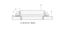
図7は本発明の第4の実施形態を示すものである。この実施形態は、プリント配線基板4の演算素子6と対向する部位に1または複数個の貫通孔(浸入防止部)14を形成したことを特徴とするものである。貫通孔14を1個設ける場合には、演算素子6と対向する部位の中央部に設けることが好ましい。本実施形態では、複数個の貫通孔14を、演算素子6と対向する部位の周囲部に設けている。
[Fourth Embodiment]
FIG. 7 shows a fourth embodiment of the present invention. This embodiment is characterized in that one or a plurality of through holes (intrusion prevention portions) 14 are formed in a portion of the printed
このように構成した場合には、防湿剤11の塗布時に、防湿剤11が演算素子6とプリント配線基板4との間の隙間内に浸入するが、その浸入した防湿剤11は、貫通孔14を通じて演算素子6とプリント配線基板4との間の隙間内から外へと抜け出る。このため、演算素子6とプリント配線基板4との間の隙間内に残る防湿剤11の量が少なくなり、その結果、演算素子6が持ち上げられるようなことがなくなり、或いは演算素子6の持ち上げられる応力や上方への動き量が軽減されるようになるので、半田9の疲労を極力防止することができる。
When configured in this way, the moisture-
[その他の実施形態]
本発明は上記し且つ図面に示す実施形態に限定されるものではなく、以下のような拡張或いは変更が可能である。
本発明を適用する電子装置は、演算素子6に限られず、QFP型の半導体パッケージに広く適用でき、更には、QFP型の半導体パッケージやその他の型の半導体パッケージに限られず、側面から多数のリードが取り出された電子装置を基板に半田付けする場合に広く適用することができる。また、パッケージ底部に電極のあるものなど、半田により表面実装で基板上に取り付ける電子装置にも一般的に応用できる。
更に、防湿剤に限らず、基板と電子装置の間に樹脂が浸透し、硬化後熱応力がかかるもの、例えばゲル状の保護剤やポッティング、コーティング剤の場合にも使用することができる。
浸入防止部は、防湿剤を塗布する部分、即ち電子装置のリードが設けられている部分に対応して設ければ良い。例えば、電子装置の四側面のうちニ側面だけにリードが設けられている場合、浸入防止部は、電子装置のリードのある二側面に対応して設ければ良いものである。
[Other Embodiments]
The present invention is not limited to the embodiment described above and shown in the drawings, and can be expanded or changed as follows.
The electronic device to which the present invention is applied is not limited to the
Further, the present invention is not limited to a moisture-proofing agent, and can be used in the case of a resin that penetrates between a substrate and an electronic device and is subjected to thermal stress after curing, such as a gel-like protective agent, potting, or coating agent.
The intrusion prevention unit may be provided corresponding to a portion where the moisture-proofing agent is applied, that is, a portion where the lead of the electronic device is provided. For example, when leads are provided on only two side surfaces of the four side surfaces of the electronic device, the intrusion prevention unit may be provided corresponding to the two side surfaces of the electronic device with the leads.
図面中、2は蓋板、3はケース、4はプリント配線基板、6は演算素子(電子装置)、6aは裏面(基板側端面)、7はリード、8はランド、9は半田、10は囲壁(浸入防止部)、11は防湿剤、12は囲壁(浸入防止部)、13は溝(浸入防止部)、14は貫通孔(浸入防止部)を示す。
In the drawings, 2 is a cover plate, 3 is a case, 4 is a printed wiring board, 6 is an arithmetic element (electronic device), 6a is a back surface (substrate-side end surface), 7 is a lead, 8 is a land, 9 is solder, 10 is
Claims (8)
前記基板および前記電子装置のうちの少なくとも一方に、前記電子装置と前記基板との間の隙間内への前記防湿剤の浸入を防止するため浸入防止部を設け、
前記浸入防止部は、前記基板において前記電子装置に覆われた領域に設けられた該電子装置方向に開口を有する溝であることを特徴とする電子装置の実装構造。 In the mounting structure of an electronic device formed by soldering an electronic device in which a plurality of leads protrude from the side surface onto a substrate and applying a moisture-proofing agent to the lead,
At least one of the substrate and the electronic device is provided with an intrusion prevention portion for preventing the moisture-proofing agent from entering the gap between the electronic device and the substrate ,
The electronic device mounting structure , wherein the intrusion prevention portion is a groove provided in a region of the substrate covered by the electronic device and having an opening in the direction of the electronic device.
前記基板および前記電子装置のうちの少なくとも一方に、前記電子装置と前記基板との間の隙間内への前記防湿剤の浸入を防止するため浸入防止部を設け、At least one of the substrate and the electronic device is provided with an intrusion prevention portion for preventing the moisture-proofing agent from entering the gap between the electronic device and the substrate,
前記浸入防止部は、前記防湿剤を裏面に排出する貫通孔であることを特徴とする電子装置の実装構造。The electronic device mounting structure, wherein the intrusion prevention unit is a through hole for discharging the moisture-proof agent to the back surface.
前記囲壁により囲まれた領域は中空となっていることを特徴とする請求項4に記載の電子装置の実装構造。5. The electronic device mounting structure according to claim 4, wherein a region surrounded by the surrounding wall is hollow.
Priority Applications (1)
| Application Number | Priority Date | Filing Date | Title |
|---|---|---|---|
| JP2008100268A JP5056552B2 (en) | 2008-04-08 | 2008-04-08 | Electronic device mounting structure |
Applications Claiming Priority (1)
| Application Number | Priority Date | Filing Date | Title |
|---|---|---|---|
| JP2008100268A JP5056552B2 (en) | 2008-04-08 | 2008-04-08 | Electronic device mounting structure |
Publications (2)
| Publication Number | Publication Date |
|---|---|
| JP2009253077A JP2009253077A (en) | 2009-10-29 |
| JP5056552B2 true JP5056552B2 (en) | 2012-10-24 |
Family
ID=41313483
Family Applications (1)
| Application Number | Title | Priority Date | Filing Date |
|---|---|---|---|
| JP2008100268A Expired - Fee Related JP5056552B2 (en) | 2008-04-08 | 2008-04-08 | Electronic device mounting structure |
Country Status (1)
| Country | Link |
|---|---|
| JP (1) | JP5056552B2 (en) |
Families Citing this family (1)
| Publication number | Priority date | Publication date | Assignee | Title |
|---|---|---|---|---|
| CN115802739B (en) * | 2022-10-26 | 2025-03-25 | 北京控制工程研究所 | A mounting structure for SOP packaged devices of aerospace electronic products |
Family Cites Families (4)
| Publication number | Priority date | Publication date | Assignee | Title |
|---|---|---|---|---|
| JPH04118951A (en) * | 1990-09-10 | 1992-04-20 | Hitachi Ltd | semiconductor package structure |
| JPH06209054A (en) * | 1993-01-08 | 1994-07-26 | Mitsubishi Electric Corp | Semiconductor device |
| JPH06283628A (en) * | 1993-03-26 | 1994-10-07 | Matsushita Electric Ind Co Ltd | Hybrid integrated circuit device |
| JP2973940B2 (en) * | 1996-09-20 | 1999-11-08 | 日本電気株式会社 | Element resin sealing structure |
-
2008
- 2008-04-08 JP JP2008100268A patent/JP5056552B2/en not_active Expired - Fee Related
Also Published As
| Publication number | Publication date |
|---|---|
| JP2009253077A (en) | 2009-10-29 |
Similar Documents
| Publication | Publication Date | Title |
|---|---|---|
| US8035208B2 (en) | Integrated circuit package | |
| US9446941B2 (en) | Method of lower profile MEMS package with stress isolations | |
| JP5157967B2 (en) | Sensor device and its mounting structure | |
| CN101852811B (en) | Sensor assembly | |
| JP6105087B2 (en) | Overmolded device with MEMS parts and manufacturing method | |
| ITMI20001335A1 (en) | PROCEDURE TO DROP A GROUP EQUIPPED WITH MASSACULATED ANTI-VIBRATION BY CASTING | |
| JP6092684B2 (en) | Physical quantity sensor device | |
| US8049290B2 (en) | Integrated circuit package | |
| JP2017228779A (en) | Optical sealing structure | |
| KR20150097628A (en) | Method for producing an electronic assembly | |
| CN105466627A (en) | Sensor module for measuring a pressure of a fluid | |
| US8664758B2 (en) | Semiconductor package having reliable electrical connection and assembling method | |
| CN105611774A (en) | System including sensor and electrical cable | |
| JP5056552B2 (en) | Electronic device mounting structure | |
| US20150300905A1 (en) | Semiconductor sensor with gel filled cavity | |
| JP6425595B2 (en) | Electronic component and method of manufacturing electronic component | |
| CN111799229B (en) | Electronic device and method for manufacturing electronic device | |
| JP2016100403A (en) | Temperature / humidity / pressure integrated sensor | |
| JP2009516159A (en) | Sensor, sensor element and sensor manufacturing method | |
| CN112897451A (en) | Sensor packaging structure, manufacturing method thereof and electronic equipment | |
| CN107295741B (en) | Electronic unit with ESD protection device | |
| JP6083357B2 (en) | Electronic equipment | |
| US20060097405A1 (en) | IC chip package and method for packaging same | |
| CN118647569A (en) | Assembly device for housing and manufacturing method | |
| JP3320610B2 (en) | Electronic device sealing structure |
Legal Events
| Date | Code | Title | Description |
|---|---|---|---|
| A621 | Written request for application examination |
Free format text: JAPANESE INTERMEDIATE CODE: A621 Effective date: 20100125 |
|
| A977 | Report on retrieval |
Free format text: JAPANESE INTERMEDIATE CODE: A971007 Effective date: 20100408 |
|
| A131 | Notification of reasons for refusal |
Free format text: JAPANESE INTERMEDIATE CODE: A131 Effective date: 20120417 |
|
| A521 | Written amendment |
Free format text: JAPANESE INTERMEDIATE CODE: A523 Effective date: 20120612 |
|
| TRDD | Decision of grant or rejection written | ||
| A01 | Written decision to grant a patent or to grant a registration (utility model) |
Free format text: JAPANESE INTERMEDIATE CODE: A01 Effective date: 20120703 |
|
| A01 | Written decision to grant a patent or to grant a registration (utility model) |
Free format text: JAPANESE INTERMEDIATE CODE: A01 |
|
| A61 | First payment of annual fees (during grant procedure) |
Free format text: JAPANESE INTERMEDIATE CODE: A61 Effective date: 20120716 |
|
| FPAY | Renewal fee payment (event date is renewal date of database) |
Free format text: PAYMENT UNTIL: 20150810 Year of fee payment: 3 |
|
| R151 | Written notification of patent or utility model registration |
Ref document number: 5056552 Country of ref document: JP Free format text: JAPANESE INTERMEDIATE CODE: R151 |
|
| FPAY | Renewal fee payment (event date is renewal date of database) |
Free format text: PAYMENT UNTIL: 20150810 Year of fee payment: 3 |
|
| R250 | Receipt of annual fees |
Free format text: JAPANESE INTERMEDIATE CODE: R250 |
|
| R250 | Receipt of annual fees |
Free format text: JAPANESE INTERMEDIATE CODE: R250 |
|
| R250 | Receipt of annual fees |
Free format text: JAPANESE INTERMEDIATE CODE: R250 |
|
| R250 | Receipt of annual fees |
Free format text: JAPANESE INTERMEDIATE CODE: R250 |
|
| R250 | Receipt of annual fees |
Free format text: JAPANESE INTERMEDIATE CODE: R250 |
|
| LAPS | Cancellation because of no payment of annual fees |