JP5048847B2 - Digital phase locked loop with gate time / digital converter - Google Patents
Digital phase locked loop with gate time / digital converter Download PDFInfo
- Publication number
- JP5048847B2 JP5048847B2 JP2010541500A JP2010541500A JP5048847B2 JP 5048847 B2 JP5048847 B2 JP 5048847B2 JP 2010541500 A JP2010541500 A JP 2010541500A JP 2010541500 A JP2010541500 A JP 2010541500A JP 5048847 B2 JP5048847 B2 JP 5048847B2
- Authority
- JP
- Japan
- Prior art keywords
- signal
- reference signal
- clock
- main
- enable
- Prior art date
- Legal status (The legal status is an assumption and is not a legal conclusion. Google has not performed a legal analysis and makes no representation as to the accuracy of the status listed.)
- Active
Links
Images


Classifications
-
- H—ELECTRICITY
- H03—ELECTRONIC CIRCUITRY
- H03L—AUTOMATIC CONTROL, STARTING, SYNCHRONISATION OR STABILISATION OF GENERATORS OF ELECTRONIC OSCILLATIONS OR PULSES
- H03L7/00—Automatic control of frequency or phase; Synchronisation
- H03L7/06—Automatic control of frequency or phase; Synchronisation using a reference signal applied to a frequency- or phase-locked loop
- H03L7/08—Details of the phase-locked loop
- H03L7/0802—Details of the phase-locked loop the loop being adapted for reducing power consumption
-
- H—ELECTRICITY
- H03—ELECTRONIC CIRCUITRY
- H03L—AUTOMATIC CONTROL, STARTING, SYNCHRONISATION OR STABILISATION OF GENERATORS OF ELECTRONIC OSCILLATIONS OR PULSES
- H03L7/00—Automatic control of frequency or phase; Synchronisation
- H03L7/06—Automatic control of frequency or phase; Synchronisation using a reference signal applied to a frequency- or phase-locked loop
- H03L7/08—Details of the phase-locked loop
- H03L7/085—Details of the phase-locked loop concerning mainly the frequency- or phase-detection arrangement including the filtering or amplification of its output signal
- H03L7/087—Details of the phase-locked loop concerning mainly the frequency- or phase-detection arrangement including the filtering or amplification of its output signal using at least two phase detectors or a frequency and phase detector in the loop
Landscapes
- Stabilization Of Oscillater, Synchronisation, Frequency Synthesizers (AREA)
- Manipulation Of Pulses (AREA)
Description
本開示は、一般に、電子装置に関し、さらに詳細にはデジタル位相ロックドループに関する。 The present disclosure relates generally to electronic devices, and more particularly to digital phase locked loops.
位相ロックドループ(PLL)は、多くの電子回路の一体化部分であり、通信回路において、特に重要である。例えば、デジタル回路は、フリップフロップなどの同期回路をトリガするためにクロックを使用する。送信機と受信機は、周波数アップコンバージョン(upconversion)および周波数ダウンコンバージョン(downconversion)のそれぞれのために、ローカル発振器(LO)信号を使用する。無線通信システムのための無線デバイス(例えば携帯電話)は、デジタル回路に対してクロックを、また、送信機と受信機に対してLO信号を典型的に使用する。クロックとLO信号は発振器で生成され、それらの周波数はしばしばPLLで制御される。 The phase locked loop (PLL) is an integral part of many electronic circuits and is particularly important in communication circuits. For example, digital circuits use a clock to trigger a synchronization circuit such as a flip-flop. The transmitter and receiver use local oscillator (LO) signals for frequency upconversion and frequency downconversion, respectively. Wireless devices (eg, mobile phones) for wireless communication systems typically use clocks for digital circuits and LO signals for transmitters and receivers. Clock and LO signals are generated by an oscillator, and their frequency is often controlled by a PLL.
PLLは、発振器からの発振器信号の周波数および/または位相を調節するために使用される様々な回路ブロックを典型的に含む。これらの回路ブロックは、比較的に大量の電力を消費し、それは携帯電話などのポータブルデバイスにとって望ましくない。従って、パフォーマンスにインパクトを与えずに、PLLの電力消費を削減することが、当技術分野において必要である。 A PLL typically includes various circuit blocks used to adjust the frequency and / or phase of an oscillator signal from an oscillator. These circuit blocks consume a relatively large amount of power, which is undesirable for portable devices such as mobile phones. Therefore, there is a need in the art to reduce PLL power consumption without impacting performance.
高性能、および、より少ない電力消費のデジタルPLL(DPLL)が本明細書に記述される。DPLLは、アナログ回路の代わりにデジタル回路を用いて実施されるPLLである。デジタル実装は、より低いコスト、より小さい回路エリアなどの利点を提供する。 A high performance and lower power digital PLL (DPLL) is described herein. DPLL is a PLL implemented using a digital circuit instead of an analog circuit. Digital implementation offers advantages such as lower cost, smaller circuit area.
ある設計において、DPLLは、動作にインパクトを与えずに電力消費を削減するために、動的に有効および無効にされる時間/デジタル変換器(TDC:time-to-digital converter)を利用する。TDCは、発振器の位相情報を量子化するために、短い時間の間、周期的に有効にされ、電力消費を削減するために、残り時間の間、無効にされる。 In one design, the DPLL utilizes a time-to-digital converter (TDC) that is dynamically enabled and disabled to reduce power consumption without impacting operation. The TDC is enabled periodically for a short time to quantize the oscillator phase information, and disabled for the remaining time to reduce power consumption.
ある設計において、DPLLはTDCおよび制御ユニットを含む。TDCは第1のクロック信号と第1の基準信号を受信し、第1のクロック信号と第1の基準信号との位相差を示すTDC出力を提供する。制御ユニットは、主基準信号に基づいて(例えば、それだけに基づいて)イネーブル信号(enable signal)を生成し、このイネーブル信号でTDCを有効(enable)および無効(disable)にする。 In one design, the DPLL includes a TDC and a control unit. The TDC receives the first clock signal and the first reference signal and provides a TDC output indicating the phase difference between the first clock signal and the first reference signal. The control unit generates an enable signal based on (eg, based on) the main reference signal, and enables and disables the TDC with this enable signal.
ある設計において、制御ユニットは、第1の基準信号を獲得するために主基準信号を第1の持続時間だけ遅らせ、第2の基準信号を獲得するために第1の基準信号を第2の持続時間だけさらに遅らせる。制御ユニットは、主基準信号と第2の基準信号に基づいてイネーブル信号を生成する。次に、制御ユニットは、第1のクロック信号を獲得するために、イネーブル信号で主クロック信号をゲートする。第1の持続時間および/または第2の持続時間はプログラム可能であり、主クロック信号の周波数に基づいて選択される。イネーブル信号は、第1と第2の持続時間の間、アクティブである。第1のクロック信号は、第1の基準信号の各リーディングエッジの周りに少なくとも1つのクロックサイクルを有し、残り時間の間、オフにゲートされる。本開示の様々な態様と特徴は、さらに詳細に以下に記述される。 In one design, the control unit delays the primary reference signal by a first duration to acquire the first reference signal and the first reference signal to the second duration to acquire the second reference signal. Delay further by time. The control unit generates an enable signal based on the main reference signal and the second reference signal. The control unit then gates the main clock signal with the enable signal to obtain the first clock signal. The first duration and / or the second duration are programmable and are selected based on the frequency of the main clock signal. The enable signal is active for the first and second durations. The first clock signal has at least one clock cycle around each leading edge of the first reference signal and is gated off for the remaining time. Various aspects and features of the disclosure are described in further detail below.
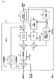
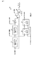
図1は、DPLL 100の設計のブロック図を示す。この設計において、DPLL 100は、広帯域変調を達成するために、2点またはデュアルポート変調を実施する。DPLL 100内で、変調信号は、ローパス変調経路とハイパス変調経路との両方に提供される。ハイパス変調経路において、スケーリングユニット110は、変調信号を受信し、利得でスケールしてスケールされた変調信号を提供する。ローパス変調経路において、加算器112は、変調信号を受信して、通信に使用される周波数チャネルの中心周波数の静的数値と合計する。入力累算器114は、加算器112の出力を累算し、入力位相を提供する。累算は、本質上、周波数を位相に変換する。入力累算器114は、frefという固定周波数を有する基準(REF)信号によってトリガされる。DPLL 100内の様々な回路ブロックと信号は、REF信号でアップデートされ、tは、REF信号のためのインデックスである。
FIG. 1 shows a block diagram of the
加算器116は、フィードバック位相を受信して、入力位相からフィードバック位相を減算し、位相誤差を提供する。ループフィルタ118は、位相誤差をフィルタし、フィルタされた位相誤差を提供する。ループフィルタ118は、DPLL 100のループダイナミクスを設定する。加算器120は、ループフィルタ118からのフィルタされた位相誤差とスケーリングユニット110からのスケールされた変調信号とを合計し、発振器130に制御信号を提供する。制御信号は、発振器の位相が変調の位相に続くように、発振器130の周波数を調節する。制御信号は、任意のビット数の分解度(resolution)、例えば、8、12、16、20、24、またはそれ以上のビットの分解度を有する。
変調信号の帯域幅は、DPLL 100が使用されるアプリケーションによって決定され、DPLLの閉ループ帯域幅よりも広い。ローパス変調経路の帯域幅はループフィルタ118によって決定され、所望の雑音除去およびループダイナミクスを達成するために比較的に狭い(例えば、100KHz以下)。個々のハイパスおよびローパス変調経路を介して変調信号を適用することで、DPLL 100 はDPLLの閉ループ帯域幅より広い信号帯域幅で発振器130を変調することができる。スケーリングユニット110の利得は、2005年6月21に発行された「PHASE LOCKED LOOP HAVING A FORWARD GAIN ADAPTATION MODULE」と題する米国特許番号6,909,331に記述されるように決定される。
The bandwidth of the modulated signal is determined by the application in which
発振器130は、デジタル制御発振器(DCO:digitally controlled oscillator)、電圧制御発振器(VCO:voltage controlled oscillator)、電流制御発振器(ICO:current controlled oscillator)、または、その周波数が制御信号によって調節される幾つかの別のタイプの発振器である。発振器130は、DPLL 100が使用されるアプリケーションによって決定されるfoscという公称周波数で動作する。例えば、DPLL 100は無線通信デバイスのために使用され、foscは数百メガヘルツ(MHz)、または、数ギガヘルツ(GHz)である。REF信号は、水晶発振器(XO:crystal oscillator)、電圧制御水晶発振器(VCXO:voltage controlled crystal oscillator)、温度補償水晶発振器(TCXO:temperature compensated crystal oscillator)または正確な周波数を有する幾つかの別のタイプの発振器に基づいて生成される。REF信号の周波数は、発振器信号の周波数よりも非常に低い。例えば、foscが数GHzであるのに対して、frefは数十MHzである。
The
DPLL 100のフィードバック経路において、分割器132は、発振器130から発振器信号を受信し、整数要素(例えば、1、2、3、4など)で発振器信号を周波数に分割し、無線周波数(RF)クロックを提供する。RF累算器140は、各RFクロック周期に対して1つ増す。ラッチ142は、REF信号によってトリガされた時、RF累算器140の出力をラッチし、粗い出力位相を提供する。TDC 150は、RFクロックとREF信号とを受信し、REF信号によってトリガされる時、RFクロックの位相を決定し、RFクロックとREF信号との間の精細な位相差を示すTDC出力を提供する。TDC 150は、REF信号の分解度を超えて発振器130の位相情報を量子化し、DPLL 100のための細分位相センサ(fractional phase sensor)を実現する。加算器144は、ラッチ142からの粗い出力位相とTDC出力とを合計し、発振器130の位相の推定であるフィードバック位相を提供する。
In the
デジタル回路による電力消費量は、典型的に、デジタル回路をトリガするために使用されるクロックの周波数に関係する。DPLL 100内の回路ブロックの大部分は、比較的に低い周波数を有するREF信号に基づいて動作する。RF累算器140とTDC 150は、周波数において、REF信号よりも何倍も高いRFクロックに基づいて動作する。従って、RF累算器140とTDC 150は、DPLL 100の合計電力消費の大部分(例えば、約50%)の要因である。分割器132は、発振器信号を分割してより低い周波数でRFクロックを提供し、RF累算器140およびTDC 150による電力消費を削減する。さらなる電力削減は、DPLL 100がロックされた後に、RF累算器140を無効にすることによって達成される。本願と同一人に譲渡され、2007年11月29日に出願された「DIGITAL PHASE-LOCKED LOOP OPERATING BASED ON FRACTIONAL INPUT AND OUTPUT PHASES」と題する米国特許出願11/947,587に記述されるように、RF累算器140が無効状態の時、位相誤差は、TDC 150からの精細な出力位相と、入力累算器114からの入力位相の精細な部分とに基づいて決定される。さらなる電力削減は、以下に示されるように、動的にTDC 150をオンとオフにゲートすることで達成される。
The power consumption by a digital circuit is typically related to the frequency of the clock used to trigger the digital circuit. Most of the circuit blocks in
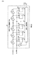
図2は、図1におけるTDC 150の設計の概略図を示す。TDC 150は、RFクロックの位相とREF信号の位相を比較し、検出された位相差に複数(B個)のビットの分解度を提供する。TDC 150は、Z=2B個の遅延要素210aから210z、Z個のDフリップフロップ220aから220z、温度計/2値変換器(thermometer-to-binary converter)230を含む。遅延要素210aから210zは、遅延要素210aがRFクロックを受信する状態で直列結合される。各遅延要素210は、所望の遅延分解度を獲得するために、インバータおよび/または別のタイプの論理要素と共に実装される。遅延要素210aから210zは、およそ1RFクロック周期の合計遅延を提供する。例えば、RFクロック周波数が2GHzの場合、1RFクロック周期は500ピコセカンド(ps)であり、各遅延要素210は、約500/Z psの遅延を提供する。
FIG. 2 shows a schematic diagram of the design of
Dフリップフロップ220aから220zは、遅延要素210aから210zの出力にそれぞれ結合されたD入力、および、REF信号を受信するクロック入力を有する。各Dフリップフロップ220は、関連する遅延要素210の出力をサンプリングし、サンプリングされた出力を変換器230に提供する。論理ハイでのDフリップフロップ数に対する論理ローでのDフリップフロップの数は、RFクロックとREF信号との間の位相差を示す。この位相差は1/Z RFクロック周期の分解度を有する。インバータ228は、REF信号を受信し、反転REF信号を変換器230に提供する。変換器230は、Dフリップフロップ220aから220zからのZ個の出力を受信し、反転REF信号によってトリガされる時に、Z個の出力をBビット2進値に変換し、Bビット2進値をTDC出力として提供する。
D flip-flops 220a through 220z have a D input coupled to the outputs of
一般に、TDC 150 は、任意のビット数の分解度で設計される。例えば、Bは、所望の遅延分解度、所与の集積回路(IC)プロセスでの利用可能な最小遅延などに依存して、8またはそれ以上である。所望の遅延分解度は、DPLL 100が使用されるアプリケーション、RFクロック周波数などに依存する。
In general, the
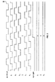
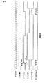
図3は、図2におけるTDC 150内での様々な信号のタイミング図を示す。RFクロックは、図3の上部に示される。遅延要素210aから210zそれぞれからのZ個の遅延信号D1からDZは、RFクロックの下に示される。D1信号からDZ信号は、遅延要素が増えるに従ってより多くの量、遅らされる。D1信号からDZ信号は、REF信号のリーディング/立上がりエッジでラッチされ、それは、これら遅延信号のリーディングエッジに関係する任意の時間に常に発生する。Dフリップフロップ220a−220zそれぞれからのZ個のラッチ信号Q1からQZは、変換器230に提供される。
FIG. 3 shows a timing diagram of various signals within the
上に示されるように、RFクロック周波数は、REF信号周波数より何倍も高い。例えば、RFクロックは2GHz、REF信号は57MHz、そして、約35のRFクロック周期が各REF信号周期に存在する。Z個の遅延要素210aから210zはRFクロックで動作し、それらの出力は各RFクロック周期で移行する。さらに、精細な位相分解度を獲得するために、直列結合される多くの遅延要素210が存在する。従って、遅延要素210は、高い動作周波数と多数の遅延要素のため、大量の電力を消費する。
As shown above, the RF clock frequency is many times higher than the REF signal frequency. For example, the RF clock is 2 GHz, the REF signal is 57 MHz, and there are about 35 RF clock periods in each REF signal period. The
ある態様において、位相情報を記憶するために少しの時間の間、TDCを動的に有効にし、残り時間の間、TDCを動的に無効にすることで、より少ない電力消費がTDC 150のために達成される。これは、REF信号の各リーディングエッジの周りの小ウィンドウ期間以外でRFクロックをオフにゲートすることで達成される。図3に示されるように、Z個の遅延要素210aから210zの出力は、REFシグナル周期毎に1度だけ獲得される。REF信号は、各リーディングエッジの周りに小ウィンドウを生成するために使用される。TDC 150は、位相情報を獲得するために、この小ウィンドウ内で有効にされ、電力を節約するために、ウィンドウの外で無効にされる。
In some aspects, TDC is dynamically enabled for a small amount of time to store phase information, and TDC is dynamically disabled for the remaining time, resulting in less power consumption for
図4は、ゲートTDC(gated TDC)を有するDPLL 400の設計のブロック図を示す。この設計において、DPLL 400は図1のDPLL 100内の全ての回路ブロックを含む。DPLL 400は、分割器132からのRFクロックおよびREF信号を受信するクロック制御ユニット148をさらに含む。制御ユニット148は、REF信号のリーディングエッジの周りの僅かな時間の間だけ有効にされたゲートRFクロック(gated RF clock)を生成する。制御ユニット148は、また、TDC 150のための第1の基準(REF1)信号、および、入力累算器114、ラッチ142、DPLL 400内の別のブロックのための別の基準(REFA)信号を生成する。
FIG. 4 shows a block diagram of a design of
図5は、図4におけるクロック制御ユニット148内の様々な信号のタイミング図を示す。RFクロックは図5の上部に示され、REF信号はRFクロックの下に示される。REF1信号は、持続時間Tdelay1だけREF信号を遅らせることで獲得される。第2の基準(REF2)信号は、持続時間Tdelay2だけREF1を遅らせることで獲得される。イネーブル信号は、REF信号およびREF2信号に基づいて生成される。イネーブル信号は、REF信号のリーディングエッジからREF2信号のリーディングエッジまでの間、論理ハイであり、残り時間の間は論理ローである。RFクロックは、RFクロックの1つ以上の周期を含むゲートRFクロックを生成するために、イネーブル信号でゲートされる。REF信号のリーディングエッジは、RFクロックゲーティング(RF clock gating)をオンにするために使用される。REF2信号のリーディングエッジは、RFクロックゲーティングをオフにするために使用される。REF1信号のリーディングエッジは、TDC 150内のコア回路をトリガして有効にするために使用される。
FIG. 5 shows a timing diagram of various signals within the
図2を再度参照して、ゲートRFクロック(RFクロックの代わりに)が遅延要素210aに提供されてもよい。REF1信号(REF信号の代わりに)がDフリップフロップ220aから220zのクロック入力とインバータ228とに提供されてもよい。
Referring back to FIG. 2, a gated RF clock (instead of an RF clock) may be provided to the
図6は、ゲートRFクロックと共に、図2のTDC 150内の様々な信号のタイミング図を示す。RFクロックおよびイネーブル信号が、参照のために図6の上部に示される。ゲートRFクロックは、イネーブル信号の下に示される。遅延要素210aから210zそれぞれからのZ個の遅延信号D1からDZは、ゲートRFクロックの下に示される。D1からDZ信号は、イネーブル信号上のアクティブウィンドウの間で生じるREF1信号のリーディングエッジによってラッチされる。Dフリップフロップ220aから220zそれぞれからのZ個のラッチ信号Q1からQZは、変換器230に提供される。
FIG. 6 shows a timing diagram of various signals within the
図6に示されるように、TDC 150の機能性は、発振器130の位相情報が短い時間の間のみ必要であるため、RFクロックをオン/オフにゲートすることによって影響されない。ゲートRFクロックと、D1からDZ信号は、REF1信号の各リーディングエッジの周りの時間の間、有効である。一般に、ゲートRFクロックは、REF1信号のリーディングエッジより前の任意の数のRFクロック周期、および、リーディングエッジの後の任意の数のRFクロック周期に対して有効である。しかし、電力消費を削減するために、ゲートRFクロック中のクロック周期の数を最小化することが望まれる。イネーブル信号は、1個または2個だけのRFクロック周期を通すために生成される。ある設計において、イネーブル信号は、リーディングエッジよりも前に、約1個のRFクロック周期を通し、REF1信号のリーディングエッジの後に、約1個のRFクロック周期を通す。動的にTDC 150を制御し、必要な時にのみTDCを有効にすることによって、TDC 150のための電力の大部分(例えば、90%)がセーブされる。
As shown in FIG. 6, the functionality of
図7は、図4におけるクロック制御ユニット148の設計の概略図を示す。制御ユニット148内で、プログラマブル遅延ユニット712は、REF信号を受信して、時間Tdelay1だけ遅らせ、REF1信号を提供する。プログラマブル遅延ユニット714は、REF1信号を受信し、時間Tdelay2だけ遅らせ、REF2信号を提供する。イネーブル信号上のアクティブウィンドウの期間、および、このウィンドウに関係するREF1信号のリーディングエッジの位置は、一定または設定可能な遅延であるTdelay1およびTdelay2によって決定される。インバータ716は、REF2信号を反転し、反転REF2信号を提供する。ANDゲート718は、反転REF2信号とREF信号を受信し、イネーブル信号を提供する。ANDゲート720は、イネーブル信号とRFクロックを受信し、ゲートRFクロックに提供する。ANDゲート720はRFクロックをオンおよびオフに切り替えるゲート回路である。
FIG. 7 shows a schematic diagram of a design of
Dフリップフロップ722および724は、直列結合される。Dフリップフロップ722は、D入力でREF1信号を受信し、クロック入力でRFクロックを受信する。Dフリップフロップ724は、D入力でDフリップフロップ722のQ出力を、クロック入力でRFクロックを受信し、REFA信号を提供する。Dフリップフロップ722および724はREF1信号を再クロック(reclock)し、REFA信号がRFクロックと時間整列される。
D flip-
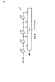
図8は、プログラマブル遅延ユニット714にも使用されうるプログラマブル遅延ユニット712の設計の概略図を示す。この設計において、プログラマブル遅延ユニット712は、直列結合されたK個の遅延要素810aから810kを含む。遅延要素810aはREF信号を受信する。マルチプレクサ(Mux)820は、遅延要素810aから810kの出力を受信し、1つの遅延要素810の出力をREF1信号として提供する。セレクト信号は、所望の量の遅延を獲得するために、遅延要素810の適当な数を選択する。選択できる遅延要素810の数は、RFクロックの周波数、各遅延要素から提供された遅延量などの様々な要因に基づく。
FIG. 8 shows a schematic diagram of a design of a
ある設計において、プログラマブル遅延ユニット712による遅延量Tdelay1、および/または、プログラマブル遅延ユニット714による遅延量Tdelay2は、RFクロック周波数に基づいて変化する。例えば、発振器130は、1.5GHzと4GHzとの間で動作し、Tdelay1および/またはTdelay2はRFクロック周波数に反比例する。
In one design, the delay amount T delay1 due to the
図4と図7は、RFクロックをオンおよびオフにゲートすることによってTDC 150が有効および無効にされる設計を示す。TDC 150は、また、電力消費を削減するために、別の方法においても有効および無効にされる。
4 and 7 show a design in which the
図9は、ゲートTDCを有するDPLLを動作するためのプロセス900の設計を示す。イネーブル信号は、主基準信号(例えば、REF信号)に基づいて(例えば、それだけに基づいて)生成される(ブロック912)。ブロック912のある設計において、主基準信号は、第1の基準信号(例えば、REF1信号)を獲得するために第1の持続時間だけ遅らせられ、第1の基準信号は、第2の基準信号(例えば、REF2信号)を獲得するために、第2の持続時間だけ遅らせられる。第1および/または第2の持続時間は、プログラム可能であり、主クロック信号(例えば、RFクロック)の周波数に基づいて選択されうる。イネーブル信号は、主基準信号および第2の基準信号(例えば、図7に示されるように)に基づいて生成され、第1と第2の持続時間、アクティブである。主クロック信号は発振器から直接的に、または、周波数において発振器の出力を分割することで獲得される。
FIG. 9 shows a design of a
TDCは、イネーブル信号に基づいて有効および無効にされる(ブロック914)。ブロック914のある設計において、主クロック信号は、第1のクロック信号(例えば、ゲートRFクロック)を獲得するために、イネーブル信号でゲートされる。主クロック信号は連続的である。第1のクロック信号は、第1の基準信号の各リーディングエッジの周りに少なくとも1つのクロック周期を有し、残り時間の間、オフにゲートされる。TDCは、ゲートされた第1クロック信号に基づいて、有効および無効にされる。TDCは、また、別の方法で有効および無効にされる。第1のクロック信号と第1の基準信号との位相差を示すTDC出力は、TDCが有効な時に獲得される(ブロック916)。RF累算器は、DPLLがロックされていない時に有効にされ、DPLLがロックされた後に無効にされる(ブロック918)。
The TDC is enabled and disabled based on the enable signal (block 914). In one design of
本明細書に記述されるゲートTDCを有するDPLLは、通信、計算、ネットワーク、パーソナル電子機器などの様々なアプリケーションに使用されうる。例えば、DPLLは、無線通信デバイス、携帯電話、携帯無線端末(PDA)、ハンドヘルデバイス、ゲーミングデバイス、処理デバイス、ラップトップコンピュータ、家庭用電子機器、パーソナルコンピュータ、コードレス電話などのために使用される。無線通信デバイスにおけるDPLLの使用例は、以下に記述される。 A DPLL with a gated TDC as described herein may be used for various applications such as communications, computing, networking, personal electronics, and the like. For example, DPLL is used for wireless communication devices, mobile phones, portable wireless terminals (PDAs), handheld devices, gaming devices, processing devices, laptop computers, consumer electronics, personal computers, cordless phones, etc. . An example use of DPLL in a wireless communication device is described below.
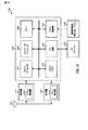
図10は、無線通信システムのための無線通信デバイス1000の設計のブロック図を示す。無線デバイス1000は、携帯電話、端末、ハンドセット、無線モデムなどである。無線通信システムは、符号分割多元接続(CDMA)システム、汎ヨーロッパデジタル移動通信システム(GSM)システムなどである。
FIG. 10 shows a block diagram of a design of a
無線デバイス1000は、受信経路および送信経路を介して、二方向通信を提供することができる。受信経路上で、基地局(図示されない)によって送信される信号は、アンテナ1010によって受信され、受信機1012に提供される。受信機1012は、受信信号を調整してデジタル化し、さらなる処理のためにセクション1020にサンプルを提供する。送信経路上で、送信機1016は、セクション1020から送信されるデータを受信し、そのデータを処理および調整し、アンテナ1010を介して基地局に送信される変調信号を生成する。受信機1012および送信機1016は、CDMA、GSMなどをサポートする。
The
セクション1020は、モデムプロセッサ1022、縮小命令セットコンピュータ/デジタル信号プロセッサ(RISC/DSP)1024、コントローラ/プロセッサ1026、メモリ1028、入力/出力(I/O)回路1030、DPLL/発振器1032などの様々な処理ユニット、インターフェースユニットおよびメモリユニットを含む。モデムプロセッサ1022は、データ送信および受信のための処理(例えば、符号化、変調、復調、復号)を実行する。RISC/DSP1024は、無線デバイス1000のための一般的および専門的な処理を実行する。コントローラ/プロセッサ1026は、セクション1020内の様々なユニットの動作を指揮する。メモリ1028は、セクション1020内の様々なユニットのためのデータおよび/または命令を記憶する。I/O回路1030は、外付けI/Oデバイス1040と通信する。
DPLL/発振器1032は、セクション1020内の処理ユニットのためにクロックを生成し、REF信号も生成する。DPLL/発振器1014は、周波数ダウンコンバージョンおよび/または復調のために受信機1012によって使用される受信LO信号を生成する。DPLL/発振器1018は、周波数アップコンバージョンおよび/または変調のために送信機1016によって使用される送信LO信号を生成する。DPLL/発振器1014、1018および/または1032は、図4におけるDPLL 400および発振器130と共に実施される。基準発振器1042は、DPLL/発振器1032および/または別のDPLL/発振器のために、正確なクロック信号を生成する。基準発振器1042は、XO、VCXO、TCXOなどである。
DPLL /
本明細書に記述されるゲートTDCを有するDPLLは、受信機1012および/または送信機1016における周波数合成のために使用され、広範囲の周波数上で動作する。DPLLは、全デジタル位相ロックドループ(ADPLL)を実施するためにDCOと共に使用される。本明細書に記述されるゲートTDCを有するDPLLは、IC、アナログIC、RF IC(RFIC)、混合信号IC、特定用途向けIC(ASIC)、プリント基板(PCB)、電子デバイスなどで実施される。DPLLは、また、相補型金属酸化膜半導体(CMOS)、NチャネルMOS(NMOS)、PチャネルMOS(PMOS)、双極性接合トランジスタ(BJT)、双極性CMOS(BiCMOS)、シリコンゲルマニウム(SiGe)、砒化ガリウム(GaAs)など、様々なICプロセス技法を用いて組み立てられる。DPLLは、ディープサブミクロン(deep sub-micron)RFCMOSトランジスタで実施され、良質のパフォーマンスと高レベルの統合を達成しうる。
The DPLL with a gated TDC described herein is used for frequency synthesis at the
本明細書に記述されるゲートTDCを有するDPLLを実施する装置は、独立型デバイスであり、または、大型デバイスの一部である。デバイスは(i)独立型IC、(ii)データおよび/または命令を記憶するためのメモリICを含む1つ以上のICセット、(iii)RF受信機(RFR)またはRF送信機/受信機(RTR)などのRFIC、(iv)移動局モデム(MSM)などのASIC、(v)別のデバイス内に組み込まれたモジュール、(vi)受信機、携帯電話、無線デバイス、ハンドセット、または移動ユニット、(vii)その他、である。 An apparatus implementing a DPLL with a gated TDC as described herein is a stand-alone device or part of a larger device. The device may be (i) a stand-alone IC, (ii) one or more IC sets including a memory IC for storing data and / or instructions, (iii) an RF receiver (RFR) or an RF transmitter / receiver ( RFICs such as RTR), (iv) ASICs such as mobile station modems (MSM), (v) modules embedded in another device, (vi) receivers, mobile phones, wireless devices, handsets, or mobile units, (Vii) Others.
本開示の以上の記述は、当業者が本発明を実施及び使用することを可能にするために提供される。これらの実施形態に対する様々な変更は当業者には容易に明らかであり、本明細書において定義された包括的な原理は、本発明の精神または範囲を逸脱することなく他の実施形態に適用可能である。従って、本発明は本明細書に記載の実施形態に制限されるものではなく、本明細書で開示される原理及び新規な特徴と合致する最も広い範囲が与えられるべきである。 The previous description of the disclosure is provided to enable any person skilled in the art to make and use the invention. Various modifications to these embodiments will be readily apparent to those skilled in the art, and the generic principles defined herein may be applied to other embodiments without departing from the spirit or scope of the invention. It is. Accordingly, the present invention is not limited to the embodiments described herein, but is to be accorded the widest scope consistent with the principles and novel features disclosed herein.
Claims (20)
主基準信号に基づいてイネーブル信号を生成するように、および、前記イネーブル信号に基づいて前記TDCを有効および無効にするように構成された制御ユニットと;
を備え、
前記制御ユニットは、第2の基準信号を獲得するために前記主基準信号を遅らせ、前記主基準信号および前記第2の基準信号に基づいて前記イネーブル信号を生成するように構成された、
装置。A time / digital converter configured to receive a first clock signal and a first reference signal and to provide a TDC output indicating a phase difference between the first clock signal and the first reference signal ( TDC);
A control unit configured to generate an enable signal based on a main reference signal and to enable and disable the TDC based on the enable signal;
Equipped with a,
The control unit is configured to delay the main reference signal to obtain a second reference signal and to generate the enable signal based on the main reference signal and the second reference signal;
apparatus.
直列に結合され、前記第1のクロック信号を受信するように構成された複数の遅延要素と、
前記複数の遅延要素に結合され、データ入力で前記複数の遅延要素出力を、そして、クロック入力で前記第1の基準信号を受信するように構成された複数のフリップフロップと、
前記複数のフリップフロップの出力を受信して前記TDC出力を提供するように構成された変換器と、
を備える、請求項1の装置。The TDC is
A plurality of delay elements coupled in series and configured to receive the first clock signal;
A plurality of flip-flops coupled to the plurality of delay elements and configured to receive the plurality of delay element outputs at a data input and the first reference signal at a clock input;
A converter configured to receive the outputs of the plurality of flip-flops and provide the TDC output;
The apparatus of claim 1 comprising:
主基準信号に基づいてイネーブル信号を生成し、前記イネーブル信号に基づいて前記TDCを有効および無効にするように構成された制御ユニットと;
を備え、
前記制御ユニットは、第2の基準信号を獲得するために前記主基準信号を遅らせ、前記主基準信号と前記第2の基準信号とに基づいて前記イネーブル信号を生成するように構成された、
集積回路。A time / digital converter configured to receive a first clock signal and a first reference signal and to provide a TDC output indicative of a phase difference between the first clock signal and the first reference signal ( TDC);
A control unit configured to generate an enable signal based on a main reference signal and to enable and disable the TDC based on the enable signal;
Equipped with a,
The control unit is configured to delay the main reference signal to obtain a second reference signal and to generate the enable signal based on the main reference signal and the second reference signal;
Integrated circuit.
第2の持続時間だけ前記第1の基準信号を遅らせて前記第2の基準信号を提供するように構成された第2の遅延ユニットとを備え、
前記イネーブル信号は、前記第1および第2の持続時間、アクティブである、
請求項8の集積回路。The control unit is configured to delay the main reference signal by a first duration to provide the first reference signal;
A second delay unit configured to delay the first reference signal by a second duration to provide the second reference signal;
The enable signal is active for the first and second durations;
The integrated circuit of claim 8 .
前記イネーブル信号によって有効にされる時、時間/デジタル変換器を実行することと;
を備え、
前記イネーブル信号を生成することは、
第1の基準信号を獲得するために、第1の持続時間だけ前記主基準信号を遅らせることと、
第2の基準信号を獲得するために、第2の持続時間だけ前記第1の基準信号を遅らせることと、
前記主基準信号と前記第2の基準信号とに基づいて前記イネーブル信号を生成することと、
を備える、
デジタル位相ロックドループ(DPLL)を動作する方法。Generating an enable signal based on the main reference signal;
Executing a time / digital converter when enabled by the enable signal;
Equipped with a,
Generating the enable signal comprises:
Delaying the main reference signal by a first duration to obtain a first reference signal;
Delaying the first reference signal by a second duration to obtain a second reference signal;
Generating the enable signal based on the main reference signal and the second reference signal;
Comprising
How to operate a digital phase locked loop (DPLL).
第1のクロック信号を獲得するために前記イネーブル信号で主クロック信号をゲートすることと、なお、前記第1のクロック信号は前記第1の基準信号の各リーディングエッジの周りに少なくとも1つのクロック周期を有し、残り時間の間、オフにゲートされる;
前記第1のクロック信号と前記第1の基準信号との位相差を決定することと;
を備える、請求項12の方法。Performing the time / digital conversion is
Gating a main clock signal with the enable signal to obtain a first clock signal, wherein the first clock signal is at least one clock period around each leading edge of the first reference signal; And is gated off for the remaining time;
Determining a phase difference between the first clock signal and the first reference signal;
The method of claim 12 comprising :
前記イネーブル信号によって有効にされる時、時間/デジタル変換を実行する手段と;
を備え、
前記イネーブル信号を生成する手段は、
第1の基準信号を獲得するために、第1の持続時間だけ前記主基準信号を遅らせる手段と、
第2の基準信号を獲得するために、第2の持続時間だけ前記第1の基準信号を遅らせる手段と、
前記主基準信号と前記第2の基準信号とに基づいて前記イネーブル信号を生成する手段と、
を備える、
装置。Means for generating an enable signal based on the main reference signal;
Means for performing a time / digital conversion when enabled by the enable signal;
Equipped with a,
The means for generating the enable signal comprises:
Means for delaying the main reference signal by a first duration to obtain a first reference signal;
Means for delaying the first reference signal by a second duration to obtain a second reference signal;
Means for generating the enable signal based on the main reference signal and the second reference signal;
Comprising
apparatus.
第1のクロック信号を獲得するために前記イネーブル信号で主クロック信号をゲートする手段と、なお、前記第1のクロック信号は、前記第1の基準信号の各リーディングエッジの周りに少なくとも1つのクロック信号を有し、残り時間の間、オフにゲートされる;
前記第1のクロック信号と前記第1の基準信号との位相差を決定する手段と;
を備える、請求項15の装置。The means for performing the time / digital conversion is:
Means for gating a main clock signal with the enable signal to obtain a first clock signal, wherein the first clock signal is at least one clock around each leading edge of the first reference signal. Has a signal and is gated off for the remaining time;
Means for determining a phase difference between the first clock signal and the first reference signal;
16. The apparatus of claim 15 , comprising:
第1のクロック信号と第1の基準信号を受信し、前記第1のクロック信号と前記第1の基準信号との位相差を示すTDC出力を提供するように構成された時間/デジタル変換器(TDC)と;
主基準信号に基づいてイネーブル信号を生成し、前記イネーブル信号に基づいて前記TDCを有効および無効にするように構成された制御ユニットと;
を備え、
前記制御ユニットは、第2の基準信号を獲得するために前記主基準信号を遅らせ、前記主基準信号および前記第2の基準信号に基づいて前記イネーブル信号を生成するように構成された、
無線デバイス。A wireless device comprising a digital phase locked loop (DPLL), wherein the digital phase locked loop is
A time / digital converter configured to receive a first clock signal and a first reference signal and to provide a TDC output indicative of a phase difference between the first clock signal and the first reference signal. TDC);
A control unit configured to generate an enable signal based on a main reference signal and to enable and disable the TDC based on the enable signal;
Equipped with a,
The control unit is configured to delay the main reference signal to obtain a second reference signal and to generate the enable signal based on the main reference signal and the second reference signal;
Wireless device.
変調信号を処理し、入力位相信号を提供するように構成された第1の変調経路と;
前記変調信号を処理し、スケールされた変調信号を提供するように構成された第2の変調経路と、なお、前記入力位相信号はループフィルタの前に適用され、前記スケールされた変調信号は前記ループフィルタの後に適用される;
を備える、請求項18の無線デバイス。The DPLL is
A first modulation path configured to process the modulation signal and provide an input phase signal;
A second modulation path configured to process the modulated signal and provide a scaled modulated signal, wherein the input phase signal is applied before a loop filter, and the scaled modulated signal is Applied after the loop filter;
The wireless device of claim 18 , comprising:
Applications Claiming Priority (3)
| Application Number | Priority Date | Filing Date | Title |
|---|---|---|---|
| US11/969,359 | 2008-01-04 | ||
| US11/969,359 US8433025B2 (en) | 2008-01-04 | 2008-01-04 | Digital phase-locked loop with gated time-to-digital converter |
| PCT/US2008/088263 WO2009088790A1 (en) | 2008-01-04 | 2008-12-24 | Digital phase-locked loop with gated time-to-digital converter |
Publications (2)
| Publication Number | Publication Date |
|---|---|
| JP2011509603A JP2011509603A (en) | 2011-03-24 |
| JP5048847B2 true JP5048847B2 (en) | 2012-10-17 |
Family
ID=40473773
Family Applications (1)
| Application Number | Title | Priority Date | Filing Date |
|---|---|---|---|
| JP2010541500A Active JP5048847B2 (en) | 2008-01-04 | 2008-12-24 | Digital phase locked loop with gate time / digital converter |
Country Status (7)
| Country | Link |
|---|---|
| US (1) | US8433025B2 (en) |
| EP (1) | EP2232708B1 (en) |
| JP (1) | JP5048847B2 (en) |
| KR (1) | KR101228394B1 (en) |
| CN (1) | CN101911493B (en) |
| TW (1) | TW200943729A (en) |
| WO (1) | WO2009088790A1 (en) |
Families Citing this family (35)
| Publication number | Priority date | Publication date | Assignee | Title |
|---|---|---|---|---|
| US7759993B2 (en) * | 2008-08-06 | 2010-07-20 | Qualcomm Incorporated | Accumulated phase-to-digital conversion in digital phase locked loops |
| EP2194646B1 (en) * | 2008-12-04 | 2013-01-02 | STMicroelectronics Srl | Method of improving noise characteristics of an ADPLL and a relative ADPLL |
| US8339165B2 (en) | 2009-12-07 | 2012-12-25 | Qualcomm Incorporated | Configurable digital-analog phase locked loop |
| US8446191B2 (en) * | 2009-12-07 | 2013-05-21 | Qualcomm Incorporated | Phase locked loop with digital compensation for analog integration |
| JP5450126B2 (en) * | 2010-01-28 | 2014-03-26 | ルネサスエレクトロニクス株式会社 | ADPLL, semiconductor device and mobile phone |
| US8228106B2 (en) * | 2010-01-29 | 2012-07-24 | Intel Mobile Communications GmbH | On-chip self calibrating delay monitoring circuitry |
| JP5863160B2 (en) * | 2010-12-21 | 2016-02-16 | ローム株式会社 | Control circuit and data holding device using the same |
| KR101202742B1 (en) | 2011-04-05 | 2012-11-19 | 연세대학교 산학협력단 | Time-to-digital converters and conversion methods |
| US8390328B2 (en) * | 2011-05-13 | 2013-03-05 | Arm Limited | Supplying a clock signal and a gated clock signal to synchronous elements |
| US8373472B2 (en) * | 2011-06-20 | 2013-02-12 | Intel Mobile Communications GmbH | Digital PLL with automatic clock alignment |
| TWI440310B (en) * | 2011-08-09 | 2014-06-01 | Univ Nat Chiao Tung | Time-to-digital converter and digitally-controlled clock generator and all-digital clock generator |
| KR101787720B1 (en) | 2011-08-19 | 2017-10-18 | 건국대학교 산학협력단 | Digital phase-locked loop using frequency shift keying and the method |
| US8593182B2 (en) | 2011-10-17 | 2013-11-26 | Mediatek Inc. | Frequency synthesizer and associated method |
| US9577650B2 (en) * | 2013-02-22 | 2017-02-21 | Microchip Technology Incorporated | Phase lock loop lock indicator |
| DE102013101933A1 (en) * | 2013-02-27 | 2014-08-28 | Technische Universität Dresden | Method and arrangement for generating a clock signal by means of a phase locked loop |
| US8830110B1 (en) | 2013-03-11 | 2014-09-09 | Nvidia Corporation | Window-enabled time-to-digital converter and method of detecting phase of a reference signal |
| CN103338037B (en) * | 2013-06-19 | 2016-11-02 | 华为技术有限公司 | The method and apparatus that in a kind of phaselocked loop, clock signal turns digital signal |
| CN105281750B (en) * | 2014-06-23 | 2018-06-15 | 华邦电子股份有限公司 | Time-to-digital converter and operation method thereof |
| US9141088B1 (en) | 2014-09-17 | 2015-09-22 | Winbond Electronics Corp. | Time-to-digital converter and operation method thereof |
| US9395698B2 (en) | 2014-10-14 | 2016-07-19 | Intel Corporation | Bang-bang time to digital converter systems and methods |
| US9590644B2 (en) | 2015-02-06 | 2017-03-07 | Silicon Laboratories Inc. | Managing spurs in a radio frequency circuit |
| US9323226B1 (en) | 2015-04-08 | 2016-04-26 | IQ-Analog Corporation | Sub-ranging voltage-to-time-to-digital converter |
| KR102261300B1 (en) | 2015-06-22 | 2021-06-09 | 삼성전자주식회사 | Clock gating circuit operating at high speed |
| CN104917517B (en) * | 2015-06-26 | 2018-04-03 | 复旦大学 | For realize low-power consumption, Wide measuring range time-to-digit converter energy-saving circuit |
| US10018970B2 (en) * | 2015-09-30 | 2018-07-10 | Mediatek Inc. | Time-to-digital system and associated frequency synthesizer |
| CN105763187B (en) * | 2016-01-28 | 2018-10-09 | 深圳清华大学研究院 | Modulator and its delay automatic calibration circuit and delay control module |
| US9853807B2 (en) * | 2016-04-21 | 2017-12-26 | Taiwan Semiconductor Manufacturing Co., Ltd. | Automatic detection of change in PLL locking trend |
| US9979405B1 (en) | 2017-02-10 | 2018-05-22 | Apple Inc. | Adaptively reconfigurable time-to-digital converter for digital phase-locked loops |
| US9831888B1 (en) | 2017-06-06 | 2017-11-28 | IQ-Analog Corp. | Sort-and delay time-to-digital converter |
| US10230360B2 (en) * | 2017-06-16 | 2019-03-12 | International Business Machines Corporation | Increasing resolution of on-chip timing uncertainty measurements |
| US10461787B2 (en) | 2018-01-30 | 2019-10-29 | Silicon Laboratories Inc. | Spur mitigation for pulse output drivers in radio frequency (RF) devices |
| US10516403B1 (en) | 2019-02-27 | 2019-12-24 | Ciena Corporation | High-order phase tracking loop with segmented proportional and integral controls |
| CN111010168A (en) * | 2019-12-26 | 2020-04-14 | 华中科技大学 | Digital phase-locked loop frequency synthesizer |
| US11646743B1 (en) | 2022-03-09 | 2023-05-09 | Nxp Usa, Inc. | Digital phase-locked loop |
| US12164002B2 (en) * | 2022-12-15 | 2024-12-10 | Stmicroelectronics International N.V. | Time-to-digital converter circuit with self-testing function |
Family Cites Families (10)
| Publication number | Priority date | Publication date | Assignee | Title |
|---|---|---|---|---|
| US6593773B2 (en) * | 2001-04-25 | 2003-07-15 | Texas Instruments Incorporated | Power saving circuitry using predictive logic |
| CN1225089C (en) * | 2002-10-31 | 2005-10-26 | 百利通电子(上海)有限公司 | Digital lock phase ring for producing multiple frequency point clock signal using one time delay chain |
| US7019570B2 (en) | 2003-09-05 | 2006-03-28 | Altera Corporation | Dual-gain loop circuitry for programmable logic device |
| CN1312875C (en) * | 2004-01-05 | 2007-04-25 | 中兴通讯股份有限公司 | PHS system position synchronous method based on digital lock phase ring and realizing device |
| US20050186920A1 (en) | 2004-02-19 | 2005-08-25 | Texas Instruments Incorporated | Apparatus for and method of noise suppression and dithering to improve resolution quality in a digital RF processor |
| US7532679B2 (en) | 2004-08-12 | 2009-05-12 | Texas Instruments Incorporated | Hybrid polar/cartesian digital modulator |
| US7205924B2 (en) * | 2004-11-18 | 2007-04-17 | Texas Instruments Incorporated | Circuit for high-resolution phase detection in a digital RF processor |
| US7801262B2 (en) | 2005-10-19 | 2010-09-21 | Texas Instruments Incorporated | All digital phase locked loop architecture for low power cellular applications |
| US7629915B2 (en) | 2006-05-26 | 2009-12-08 | Realtek Semiconductor Corp. | High resolution time-to-digital converter and method thereof |
| US8045670B2 (en) * | 2007-06-22 | 2011-10-25 | Texas Instruments Incorporated | Interpolative all-digital phase locked loop |
-
2008
- 2008-01-04 US US11/969,359 patent/US8433025B2/en active Active
- 2008-12-24 KR KR1020107017349A patent/KR101228394B1/en active Active
- 2008-12-24 JP JP2010541500A patent/JP5048847B2/en active Active
- 2008-12-24 CN CN2008801238950A patent/CN101911493B/en active Active
- 2008-12-24 EP EP08869551.5A patent/EP2232708B1/en active Active
- 2008-12-24 WO PCT/US2008/088263 patent/WO2009088790A1/en not_active Ceased
- 2008-12-31 TW TW097151664A patent/TW200943729A/en unknown
Also Published As
| Publication number | Publication date |
|---|---|
| JP2011509603A (en) | 2011-03-24 |
| CN101911493B (en) | 2013-06-05 |
| WO2009088790A1 (en) | 2009-07-16 |
| KR20100099754A (en) | 2010-09-13 |
| US8433025B2 (en) | 2013-04-30 |
| EP2232708B1 (en) | 2015-08-12 |
| US20090175399A1 (en) | 2009-07-09 |
| TW200943729A (en) | 2009-10-16 |
| EP2232708A1 (en) | 2010-09-29 |
| KR101228394B1 (en) | 2013-01-31 |
| CN101911493A (en) | 2010-12-08 |
Similar Documents
| Publication | Publication Date | Title |
|---|---|---|
| JP5048847B2 (en) | Digital phase locked loop with gate time / digital converter | |
| US8145171B2 (en) | Clock clean-up phase-locked loop (PLL) | |
| US6028488A (en) | Digitally-controlled oscillator with switched-capacitor frequency selection | |
| US8878613B2 (en) | Time-to-digital converter (TDC) with improved resolution | |
| KR101141084B1 (en) | Linear phase frequency detector and charge pump for phase-locked loop | |
| CN107294530B (en) | Calibration method and apparatus for high time To Digital Converter (TDC) resolution | |
| JP5005455B2 (en) | Semiconductor integrated circuit | |
| JP2012525795A (en) | Two-point modulated digital phase-locked loop using accumulator and phase digital converter | |
| KR20090034388A (en) | Multi-Modular Divider Retiming Circuit | |
| Oh et al. | A 3.9 mW Bluetooth low-energy transmitter using all-digital PLL-based direct FSK modulation in 55 nm CMOS | |
| WO2014133783A1 (en) | Phase-locked loop using dual loop mode to achieve fast resettling | |
| US7170965B2 (en) | Low noise divider module for use in a phase locked loop and other applications | |
| US11264995B1 (en) | System and method for maintaining local oscillator (LO) phase continuity | |
| EP0841754A2 (en) | A digitally-controlled oscillator | |
| Rehman et al. | An ultra-low-power 2.4 GHz all-digital phase-locked loop with injection-locked frequency multiplier and continuous frequency tracking | |
| Choi et al. | A low power and wide range programmable clock generator with a high multiplication factor | |
| US8674741B2 (en) | Delay chain circuit | |
| Su et al. | An all-digital phase-locked loop with a multi-delay-switching TDC | |
| Li et al. | Zeroing of power supply noise sensitivity for ring oscillators operating from 1 to 4 GHz | |
| HK1133960A (en) | Multi-modulus divider retiming circuit |
Legal Events
| Date | Code | Title | Description |
|---|---|---|---|
| A131 | Notification of reasons for refusal |
Free format text: JAPANESE INTERMEDIATE CODE: A131 Effective date: 20120131 |
|
| A521 | Request for written amendment filed |
Free format text: JAPANESE INTERMEDIATE CODE: A523 Effective date: 20120426 |
|
| TRDD | Decision of grant or rejection written | ||
| A01 | Written decision to grant a patent or to grant a registration (utility model) |
Free format text: JAPANESE INTERMEDIATE CODE: A01 Effective date: 20120619 |
|
| A01 | Written decision to grant a patent or to grant a registration (utility model) |
Free format text: JAPANESE INTERMEDIATE CODE: A01 |
|
| A61 | First payment of annual fees (during grant procedure) |
Free format text: JAPANESE INTERMEDIATE CODE: A61 Effective date: 20120719 |
|
| FPAY | Renewal fee payment (event date is renewal date of database) |
Free format text: PAYMENT UNTIL: 20150727 Year of fee payment: 3 |
|
| R150 | Certificate of patent or registration of utility model |
Ref document number: 5048847 Country of ref document: JP Free format text: JAPANESE INTERMEDIATE CODE: R150 Free format text: JAPANESE INTERMEDIATE CODE: R150 |
|
| R250 | Receipt of annual fees |
Free format text: JAPANESE INTERMEDIATE CODE: R250 |
|
| R250 | Receipt of annual fees |
Free format text: JAPANESE INTERMEDIATE CODE: R250 |
|
| R250 | Receipt of annual fees |
Free format text: JAPANESE INTERMEDIATE CODE: R250 |
|
| R250 | Receipt of annual fees |
Free format text: JAPANESE INTERMEDIATE CODE: R250 |
|
| R250 | Receipt of annual fees |
Free format text: JAPANESE INTERMEDIATE CODE: R250 |
|
| R250 | Receipt of annual fees |
Free format text: JAPANESE INTERMEDIATE CODE: R250 |
|
| R250 | Receipt of annual fees |
Free format text: JAPANESE INTERMEDIATE CODE: R250 |
|
| R250 | Receipt of annual fees |
Free format text: JAPANESE INTERMEDIATE CODE: R250 |
|
| R250 | Receipt of annual fees |
Free format text: JAPANESE INTERMEDIATE CODE: R250 |
|
| R250 | Receipt of annual fees |
Free format text: JAPANESE INTERMEDIATE CODE: R250 |
|
| R250 | Receipt of annual fees |
Free format text: JAPANESE INTERMEDIATE CODE: R250 |