JP5046641B2 - Charge neutralizer - Google Patents
Charge neutralizer Download PDFInfo
- Publication number
- JP5046641B2 JP5046641B2 JP2006513892A JP2006513892A JP5046641B2 JP 5046641 B2 JP5046641 B2 JP 5046641B2 JP 2006513892 A JP2006513892 A JP 2006513892A JP 2006513892 A JP2006513892 A JP 2006513892A JP 5046641 B2 JP5046641 B2 JP 5046641B2
- Authority
- JP
- Japan
- Prior art keywords
- plasma
- ion beam
- charge neutralization
- charge
- tube
- Prior art date
- Legal status (The legal status is an assumption and is not a legal conclusion. Google has not performed a legal analysis and makes no representation as to the accuracy of the status listed.)
- Expired - Fee Related
Links
Images


Classifications
-
- H—ELECTRICITY
- H01—ELECTRIC ELEMENTS
- H01J—ELECTRIC DISCHARGE TUBES OR DISCHARGE LAMPS
- H01J37/00—Discharge tubes with provision for introducing objects or material to be exposed to the discharge, e.g. for the purpose of examination or processing thereof
- H01J37/30—Electron-beam or ion-beam tubes for localised treatment of objects
- H01J37/317—Electron-beam or ion-beam tubes for localised treatment of objects for changing properties of the objects or for applying thin layers thereon, e.g. for ion implantation
- H01J37/3171—Electron-beam or ion-beam tubes for localised treatment of objects for changing properties of the objects or for applying thin layers thereon, e.g. for ion implantation for ion implantation
-
- G—PHYSICS
- G21—NUCLEAR PHYSICS; NUCLEAR ENGINEERING
- G21K—HANDLING OF PARTICLES OR IONISING RADIATION NOT OTHERWISE PROVIDED FOR; IRRADIATION DEVICES; GAMMA RAY OR X-RAY MICROSCOPES
- G21K1/00—Arrangements for handling particles or ionising radiation, e.g. focusing or moderating
- G21K1/14—Arrangements for handling particles or ionising radiation, e.g. focusing or moderating using charge exchange devices, e.g. for neutralising or changing the sign of the electrical charges of beams
-
- H—ELECTRICITY
- H01—ELECTRIC ELEMENTS
- H01J—ELECTRIC DISCHARGE TUBES OR DISCHARGE LAMPS
- H01J37/00—Discharge tubes with provision for introducing objects or material to be exposed to the discharge, e.g. for the purpose of examination or processing thereof
- H01J37/02—Details
- H01J37/026—Means for avoiding or neutralising unwanted electrical charges on tube components
-
- H—ELECTRICITY
- H05—ELECTRIC TECHNIQUES NOT OTHERWISE PROVIDED FOR
- H05H—PLASMA TECHNIQUE; PRODUCTION OF ACCELERATED ELECTRICALLY-CHARGED PARTICLES OR OF NEUTRONS; PRODUCTION OR ACCELERATION OF NEUTRAL MOLECULAR OR ATOMIC BEAMS
- H05H1/00—Generating plasma; Handling plasma
- H05H1/24—Generating plasma
- H05H1/46—Generating plasma using applied electromagnetic fields, e.g. high frequency or microwave energy
-
- H—ELECTRICITY
- H10—SEMICONDUCTOR DEVICES; ELECTRIC SOLID-STATE DEVICES NOT OTHERWISE PROVIDED FOR
- H10P—GENERIC PROCESSES OR APPARATUS FOR THE MANUFACTURE OR TREATMENT OF DEVICES COVERED BY CLASS H10
- H10P30/00—Ion implantation into wafers, substrates or parts of devices
- H10P30/20—Ion implantation into wafers, substrates or parts of devices into semiconductor materials, e.g. for doping
-
- H—ELECTRICITY
- H01—ELECTRIC ELEMENTS
- H01J—ELECTRIC DISCHARGE TUBES OR DISCHARGE LAMPS
- H01J2237/00—Discharge tubes exposing object to beam, e.g. for analysis treatment, etching, imaging
- H01J2237/004—Charge control of objects or beams
- H01J2237/0041—Neutralising arrangements
- H01J2237/0044—Neutralising arrangements of objects being observed or treated
-
- H—ELECTRICITY
- H10—SEMICONDUCTOR DEVICES; ELECTRIC SOLID-STATE DEVICES NOT OTHERWISE PROVIDED FOR
- H10P—GENERIC PROCESSES OR APPARATUS FOR THE MANUFACTURE OR TREATMENT OF DEVICES COVERED BY CLASS H10
- H10P30/00—Ion implantation into wafers, substrates or parts of devices
- H10P30/20—Ion implantation into wafers, substrates or parts of devices into semiconductor materials, e.g. for doping
- H10P30/202—Ion implantation into wafers, substrates or parts of devices into semiconductor materials, e.g. for doping characterised by the semiconductor materials
- H10P30/204—Ion implantation into wafers, substrates or parts of devices into semiconductor materials, e.g. for doping characterised by the semiconductor materials into Group IV semiconductors
-
- H—ELECTRICITY
- H10—SEMICONDUCTOR DEVICES; ELECTRIC SOLID-STATE DEVICES NOT OTHERWISE PROVIDED FOR
- H10P—GENERIC PROCESSES OR APPARATUS FOR THE MANUFACTURE OR TREATMENT OF DEVICES COVERED BY CLASS H10
- H10P30/00—Ion implantation into wafers, substrates or parts of devices
- H10P30/20—Ion implantation into wafers, substrates or parts of devices into semiconductor materials, e.g. for doping
- H10P30/21—Ion implantation into wafers, substrates or parts of devices into semiconductor materials, e.g. for doping of electrically active species
Landscapes
- Physics & Mathematics (AREA)
- Engineering & Computer Science (AREA)
- Chemical & Material Sciences (AREA)
- Analytical Chemistry (AREA)
- Spectroscopy & Molecular Physics (AREA)
- Plasma & Fusion (AREA)
- General Engineering & Computer Science (AREA)
- High Energy & Nuclear Physics (AREA)
- Electromagnetism (AREA)
- Plasma Technology (AREA)
- Physical Vapour Deposition (AREA)
- Drying Of Semiconductors (AREA)
Description
この発明は、電荷中和装置にかかり、特に半導体製造プロセスにおいて、半導体基板に不純物層を形成する際に用いられるイオン注入装置などに用いられる、電荷中和器、およびそれを用いて製造される半導体装置、これら半導体装置を搭載した液晶パネルなどの電子素子に関する。 The present invention relates to a charge neutralization apparatus, and in particular, a charge neutralizer used for an ion implantation apparatus used when forming an impurity layer on a semiconductor substrate in a semiconductor manufacturing process, and manufactured using the same. The present invention relates to a semiconductor device and an electronic element such as a liquid crystal panel on which the semiconductor device is mounted.
従来の半導体製造技術では、ボロン(B)、リン(P)、ヒ素(As)等の各種導電型の不純物を固体基体としての半導体基板表面に、イオン注入を行う方法が広く用いられている。イオン注入プロセス等に用いられるビームライン型イオン注入機では、ウェハ上のデバイスのチャージ破壊を防ぐため、またイオンビームの空間電荷効果によるビームの発散を防ぐために、低エネルギーの電子をビームプラズマ中またはウェハ表面上に供給することによって電荷の蓄積を緩和する電荷中和装置が多く用いられている。 In a conventional semiconductor manufacturing technique, a method is widely used in which ions of various conductivity types such as boron (B), phosphorus (P), and arsenic (As) are implanted into the surface of a semiconductor substrate as a solid substrate. In a beamline ion implanter used for an ion implantation process or the like, in order to prevent charge breakdown of a device on a wafer and to prevent beam divergence due to the space charge effect of the ion beam, low energy electrons are injected into the beam plasma or Charge neutralization devices are often used that relieve the accumulation of charge by supplying it onto the wafer surface.
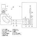
図10はイオン注入装置の中でも大電流イオン注入機と呼ばれている、メカニカルスキャン方式の従来装置の一例を示す概略図である。このイオン注入装置1は大きく3つに分けられ、それぞれ、イオン源部2、ビームライン部3、エンドステーション部4である。イオン源部2は、アーク放電によって高密度プラズマを生成するイオン源5とイオンを静電的に引き出し、加速する引き出し電極系6とで構成されている。ビームライン部3はイオン源部2より出射されたイオンビーム7から必要なドーパントイオンのみ選択する磁場偏向型の質量分析器8と、イオンビーム7の形状を整える成形スリット9や分析マグネットの焦点に位置し、必要とするドーパントイオンを選択するための分析スリット10から成る。エンドステーション部4は、ビーム電流を計測するファラデーゲージ11とビームキャッチ12、半導体基板13を載置しイオンビーム7が基板に均一に注入されるようにスキャンするディスク14、さらに電荷中和器として働く電子銃15から成る。
FIG. 10 is a schematic view showing an example of a conventional mechanical scan type apparatus called a high current ion implanter among ion implanters. The
このように構成されたイオン注入装置を用いて次のようにしてイオン注入が行われる。まず、イオン源5に必要なドーパントガスあるいは固体蒸気を用い高密度プラズマを生成する。ついで、引き出し電極系6でイオンを引き出すと同時に、所望の加速エネルギーを与える。加速されたイオンビーム7は質量分析器8で必要なドーパントイオンに選択され、成形スリット9や分析スリット10でイオンビームの形状を整えターゲットは導かれる。一方、基板13はディスク14に搬送されてきて、所定位置に載置される。このとき、基板13は通常複数枚載置される。
The ion implantation is performed as follows using the ion implantation apparatus configured as described above. First, high-density plasma is generated using a dopant gas or solid vapor necessary for the
次に、初期位置にあったディスク14が図示Aのように所定回転数で回転するとともに、並進運動Bが行われる。このような方式をメカニカルスキャン方式と呼び、これにより複数の基板13の全面にイオン注入が行われる。なお、並進運動は注入均一性を良くするため複数回行われる。
Next, the
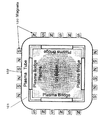
ところで、このイオン注入が行われる際、基板13上には、通常すでにゲート電極のパターンが形成されている。図11にパターニングされたものの一例を示す。同図は、基板23(13)が例えばP型であり、この基板13の主面上に厚いフィールド絶縁膜20が形成され、これら絶縁膜20に挟まれた活性領域の一部にゲート絶縁膜となる薄い絶縁膜21が形成され、この薄い酸化膜21上にゲート電極22が形成されている。この状態でイオン注入を行うことによりゲート電極22の両側の基板13上にソース・ドレインとなる不純物領域を形成するものである。この場合、ソース・ドレインをN型に形成すべく、イオンビーム7は例えばリン,ヒ素等のイオンビームとなっている。
By the way, when this ion implantation is performed, a pattern of the gate electrode is usually already formed on the
このように絶縁膜上にイオン注入を行う場合、特に1mA以上のビーム電流でイオン注入する際にはゲート絶縁膜21の絶縁破壊が発生する可能性が大となる。この絶縁破壊を防止するために、従来は図12に示すような電荷中和器が用いられている。この電荷中和器の作用は電子銃15から放出される一次電子を300V程度の電界で加速し対面するファラデーケージ11に照射し、二次電子23を発生させる。この二次電子23の一部が基板13に供給され、ゲート電極22上に蓄積された正電荷を中和する。このようにして、ゲート絶縁膜21の絶縁破壊を防止することができる。
When ion implantation is performed on the insulating film as described above, there is a high possibility that the dielectric breakdown of the
このように、従来、一般に使われている電荷中和装置では、電子源もしくはプラズマ源をビームライン上の一側面からビームに近接する形に設置し、そこから出て来る電子流をビームおよびビームプラズマに重ね合せるという方式を用いている。 As described above, in a conventional charge neutralization apparatus, an electron source or a plasma source is installed in a shape close to the beam from one side on the beam line, and the electron flow coming out of the electron source or plasma source is transmitted to the beam and beam. A method of superimposing on plasma is used.
しかし、この方法では、電子源に近い側では電荷中和効果が働いてもその反対側(電子源から最も遠い側)まで効果が及ばないという現象が発生し易く、デバイスのチャージ破壊やビームの発散を引起してしまう。 However, in this method, even if the charge neutralization effect works on the side closer to the electron source, the phenomenon that the effect does not reach the opposite side (the side farthest from the electron source) is likely to occur. It causes divergence.
また、ビームをスキャンするタイプのイオン注入機では、供給する電子流とビームプラズマとのカップリング効率が悪く、従来の電荷中和装置で高電流のイオン注入を実現することは極めて難しかった。
さらに、上記のイオン注入装置では、上述のように、電子銃15から放出した一次電子の照射によりファラデーケージ11表面から発生する二次電子23でゲート電極22上に蓄積された正電荷を中和するものであるが、一次電子の一部も反射によって基板13に到達する。このため300eVのエネルギーをもつ高速電子が基板13を負にチャージアップさせ、負電荷による絶縁破壊を起こし、また絶縁破壊に至らずとも、ゲート絶縁膜22を劣化させるという問題点があった。
Further, in the ion implanter of the type that scans the beam, the coupling efficiency between the electron flow to be supplied and the beam plasma is poor, and it has been extremely difficult to realize high current ion implantation with a conventional charge neutralization device.
Furthermore, in the above ion implantation apparatus, as described above, the positive charges accumulated on the
これに対して、図13および図14に示すように被処理基板の前面に、プラズマより電子を引き出す引き出し電極と、この引き出し電極により引き出された電子を減速する減速電極とを有し、エネルギーが50eV以下の電子を供給する磁気多極型プラズマ発生器を配設するようにした電荷中和器が開示されている(特許文献1)。これによると、磁気多極型プラズマ発生器をエレクトロンソースとしており、この磁気多極型プラズマ発生器はプラズマ内に磁場がないカスプ磁場を形成しているため、電場を印加するだけで電子温度が数eVの高密度プラズマを容易に引き出すことができる。この低エネルギー電子をターゲットとなる半導体基板前面に供給し、電子雲を発生させる。このため半導体基板上の正に帯電した部分にのみ電子が供給され電荷中和を行うことができる。このため、イオン注入条件やデバイス条件によってチャージアップ量が異なる場合でも最適な電荷中和が行えるとされている。さらに、磁気多極型プラズマ発生器を配設することで、大面積でしかも均一な電子雲を生成することができるとされている。 On the other hand, as shown in FIGS. 13 and 14, the front surface of the substrate to be processed has an extraction electrode for extracting electrons from the plasma, and a deceleration electrode for decelerating the electrons extracted by the extraction electrode. A charge neutralizer is disclosed in which a magnetic multipolar plasma generator for supplying electrons of 50 eV or less is disposed (Patent Document 1). According to this, a magnetic multipole plasma generator is used as an electron source. Since this magnetic multipole plasma generator forms a cusp magnetic field without a magnetic field in the plasma, the electron temperature can be increased by simply applying an electric field. A high-density plasma of several eV can be extracted easily. The low energy electrons are supplied to the front surface of the target semiconductor substrate to generate an electron cloud. For this reason, electrons are supplied only to the positively charged portion on the semiconductor substrate, and charge neutralization can be performed. For this reason, it is said that optimal charge neutralization can be performed even when the amount of charge-up varies depending on ion implantation conditions and device conditions. Furthermore, it is said that a uniform electron cloud having a large area can be generated by arranging a magnetic multipolar plasma generator.
従来の図12に示す電荷中和器を有するイオン注入装置では、上述のように、300eVのエネルギーをもつ高速電子が基板13を負にチャージアップさせ、負電荷による絶縁破壊を起こし、また絶縁破壊に至らずとも、ゲート絶縁膜22を劣化させるという問題点があった。さらに、電子源に近い側では電荷中和効果が働いてもその反対側(電子源から最も遠い側)まで効果が及ばないという現象が発生し易く、デバイスのチャージ破壊やビームの発散を引起してしまう。
In the conventional ion implantation apparatus having the charge neutralizer shown in FIG. 12, the high speed electrons having the energy of 300 eV cause the
また、ビームをスキャンするタイプのイオン注入機では、供給する電子流とビームプラズマとのカップリング効率が悪く、従来の電荷中和装置で高電流のイオン注入を実現することは極めて困難であった。 In addition, in a beam scanning type ion implanter, the coupling efficiency between the electron flow to be supplied and the beam plasma is poor, and it has been extremely difficult to realize high current ion implantation with a conventional charge neutralization device. .
一方、図14に示すようなエネルギーが50eV以下の電子を供給する磁気多極型プラズマ発生器を配設するようにした電荷中和器を有するイオン注入装置では、上記課題はある程度解決され、さらに大面積でしかも均一な電子雲を生成することができる。 On the other hand, in the ion implantation apparatus having a charge neutralizer in which a magnetic multipolar plasma generator for supplying electrons with energy of 50 eV or less as shown in FIG. A large area and uniform electron cloud can be generated.
しかし、デバイスの集積度の増加と共にチャージ破壊に対する許容電圧は減少し、同時にイオン注入の低エネルギー化と共にビームに対する空間電荷効果が増大するため、電荷中和装置には更なる性能の向上が求められている。上記の電荷中和装置では、特に耐圧1V以下を要求される最先端デバイスでは充分な効果が得られないという課題があった。 However, as the device integration increases, the allowable voltage for charge breakdown decreases, and at the same time, the space charge effect on the beam increases with lower energy of ion implantation. ing. The above-described charge neutralization device has a problem that a sufficient effect cannot be obtained particularly in a state-of-the-art device that requires a withstand voltage of 1 V or less.
本発明は前記実情に鑑みてなされたもので、5eV以下望ましくは2eVの水準の低エネルギーの電子を供給することで最先端デバイスに対してもイオン注入によるチャージアップと電子によるダメージをなくし、且つ、大面積の基板13に対応できる電荷中和器を提供することを目的とする。
The present invention has been made in view of the above circumstances, and by supplying low-energy electrons of 5 eV or less, preferably 2 eV, it eliminates charge-up due to ion implantation and damage due to electrons even for the most advanced devices, and An object of the present invention is to provide a charge neutralizer capable of handling a large-
本発明の第1の電荷中和装置は、マイクロ波発生手段と、前記マイクロ波発生手段で発生せしめられたマイクロ波によって電子プラズマを発生するプラズマ生成手段と、前記プラズマ生成手段で生成された電子プラズマを、イオンビームを含むビームプラズマ領域に対し、前記イオンビームを取り囲むプラズマチューブを介して、接触させる接触手段とを備え、 前記プラズマチューブ内に配置されたバイアスワイヤを介して電源から、バイアスを制御するための電位が、供給され、イオンビームに供給される電子プラズマ量を制御するように構成され、前記プラズマチューブは、イオンビームをリング状に取り囲み、前記プラズマ生成手段は、前記プラズマチューブの外側を取り囲むように配置された導波管を備え、前記マイクロ波発生手段から前記導波管を介して前記プラズマチューブ内にマイクロ波を導入するとともに前記プラズマチューブ内にガスを供給することにより、前記プラズマチューブ内にプラズマを発生させ、前記導波管は、前記導波管中のマイクロ波の伝搬方向が、前記イオンビームの流れ方向に直交する面で、前記イオンビームを囲むように配設され、前記導波管は、前記導波管中のマイクロ波伝搬方向の下流側から上流側に向かって前記プラズマチューブへのガスの供給がなされるように構成されたことを特徴とする。 The first charge neutralization apparatus of the present invention includes a microwave generating means, a plasma generating means for generating an electron plasma by a microwave generated by the microwave generating means, and an electron generated by the plasma generating means. Contact means for bringing the plasma into contact with a beam plasma region including the ion beam via a plasma tube surrounding the ion beam, and a bias from a power source via a bias wire disposed in the plasma tube. An electric potential for controlling is supplied and configured to control the amount of electron plasma supplied to the ion beam, the plasma tube surrounds the ion beam in a ring shape, and the plasma generating means is connected to the plasma tube. The microwave generating means, comprising a waveguide disposed so as to surround the outside A microwave is introduced into the plasma tube through the waveguide and gas is supplied into the plasma tube to generate plasma in the plasma tube. The waveguide is guided by the waveguide. A microwave propagation direction in the tube is disposed so as to surround the ion beam in a plane orthogonal to the ion beam flow direction, and the waveguide is arranged in the microwave propagation direction in the waveguide. A feature is that gas is supplied to the plasma tube from the downstream side toward the upstream side .
この構成により、マイクロ波によってプラズマを発生するようにしているため、効率的に、低圧でかつ高密度のプラズマを発生させ、そこから低エネルギーの電子をとりだすことができる。この装置は、通常用いられている直流放電プラズマあるいはRFプラズマなどに比べて大幅に低エネルギーのプラズマを得ることができることからきわめて有効な電荷中和手段である。そして、バイアスを制御するための電位は、プラズマチューブ内に配置されたバイアスワイヤを介して電源から供給され、イオンビームに供給される電子プラズマ量を制御するように構成されており、電子流れを増やすことができる。従って、1nm程度の薄いゲート絶縁膜をもつFETのような微細デバイスの製造に際しても、絶縁破壊が抑制され、高歩留まり化をはかることができる。
また、これにより、イオンビームを取り囲む全ての方向から電子を供給することができ、電荷中和の位置によるむらを大幅に低減することができる。
また、これにより、プラズマチューブ内に均一にプラズマを発生させ易いので望ましい。
また、この構成により、マイクロ波の減衰部により多くのガス供給がなされるためより高効率で均一なプラズマ生成が可能となる。
With this configuration, since plasma is generated by microwaves, low-pressure and high-density plasma can be efficiently generated, and low-energy electrons can be extracted therefrom. This apparatus is a very effective charge neutralization means because it can obtain a plasma having a significantly lower energy than that of a normally used DC discharge plasma or RF plasma. The potential for controlling the bias is supplied from a power source via a bias wire arranged in the plasma tube, and is configured to control the amount of electron plasma supplied to the ion beam. Can be increased. Therefore, even when a fine device such as an FET having a thin gate insulating film of about 1 nm is manufactured, dielectric breakdown can be suppressed and a high yield can be achieved.
In addition, this makes it possible to supply electrons from all directions surrounding the ion beam, and the unevenness due to the position of charge neutralization can be greatly reduced.
This is also desirable because it facilitates the uniform generation of plasma in the plasma tube.
In addition, with this configuration, a larger amount of gas is supplied to the microwave attenuating unit, so that more efficient and uniform plasma generation is possible.
また、本発明の第2の電荷中和装置は、マイクロ波発生手段と、前記マイクロ波発生手段で発生せしめられたマイクロ波によって電子プラズマを発生するプラズマ生成手段と、前記プラズマ生成手段で生成された電子プラズマを、イオンビームを含むビームプラズマ領域に対し、前記イオンビームを取り囲むプラズマチューブを介して、接触させる接触手段とを備え、前記プラズマチューブ内に配置されたバイアスワイヤを介して電源から、バイアスを制御するための電位が、供給され、イオンビームに供給される電子プラズマ量を制御するように構成され、マイクロ波励起を用いて低温プラズマを維持し、それによって2eV以下の低エネルギーの電子を供給するように構成されたことを特徴とする。
また本発明の第2の電荷中和装置は、前記接触手段がイオンビームをリング状に取り囲むプラズマチューブを有することを特徴とする。これにより、イオンビームを取り囲む全ての方向から電子を供給することができ、電荷中和の位置によるむらを大幅に低減することができる。
The second charge neutralization device of the present invention is generated by a microwave generating means, a plasma generating means for generating an electron plasma by the microwave generated by the microwave generating means, and the plasma generating means. Contact means for bringing the electron plasma into contact with a beam plasma region including an ion beam via a plasma tube surrounding the ion beam, and from a power source via a bias wire disposed in the plasma tube, A potential for controlling the bias is supplied and is configured to control the amount of electron plasma supplied to the ion beam, and maintains a low temperature plasma using microwave excitation, thereby lower energy electrons below 2 eV. It is comprised so that it may supply.
The second charge neutralization apparatus of the present invention is characterized in that the contact means has a plasma tube surrounding the ion beam in a ring shape. Thereby, electrons can be supplied from all directions surrounding the ion beam, and unevenness due to the position of charge neutralization can be greatly reduced.
また本発明の第2の電荷中和装置は、イオンビームの形状もしくはイオンビームのスキャンエリアにあわせて、前記イオンビームもしくは前記スキャンエリアの外周を取り囲む構成のプラズマチューブを有することを特徴とする。これにより、イオンビームの形状やスキャンエリアが複雑な形状をしていても、電荷中和の位置によるむらを大幅に低減することができる。 The second charge neutralization device of the present invention is characterized by having a plasma tube configured to surround the outer periphery of the ion beam or the scan area in accordance with the shape of the ion beam or the scan area of the ion beam. Thereby, even if the shape of the ion beam and the scan area are complicated, the unevenness due to the position of charge neutralization can be greatly reduced.
さらに、本発明の第2の電荷中和装置は、前記プラズマチューブの外側を取り囲む形状の導波管を配置してマイクロ波を導入することにより、前記プラズマチューブ内にプラズマを発生させることを特徴とする。これにより、プラズマチューブ内に均一にプラズマを発生させ易いので望ましい。
さらに本発明の第2の電荷中和装置は、前記導波管が、前記導波管中のマイクロ波伝搬方向の下流側から上流側に向かって前記プラズマチューブへのガスの供給がなされるように構成されるものを含む。
この構成により、マイクロ波の減衰部により多くのガス供給がなされるためより高効率で均一なプラズマ生成が可能となる。
Furthermore, the second charge neutralization device of the present invention is characterized in that a plasma is generated in the plasma tube by arranging a waveguide having a shape surrounding the outside of the plasma tube and introducing a microwave. And This is desirable because it is easy to generate plasma uniformly in the plasma tube.
Furthermore, in the second charge neutralization device of the present invention, the gas is supplied to the plasma tube from the downstream side in the microwave propagation direction in the waveguide toward the upstream side. Including those configured.
With this configuration, a larger amount of gas is supplied to the microwave attenuation section, so that more efficient and uniform plasma generation is possible.
本発明の電荷中和装置は、前記プラズマ生成手段が、同軸ケーブルであるものを含む。 In the charge neutralization apparatus of the present invention, the plasma generating means includes a coaxial cable.
また本発明の電荷中和装置は、前記プラズマチューブ内にガスを供給してプラズマを発生させることを特徴とする。これにより、高効率のプラズマ照射を実現できる。
さらに前記プラズマ発生用のガスの種類は、希ガスなどの不活性ガスであることを特徴とする。これにより、半導体などのターゲットに与える影響をほとんど無視できる水準にすることができる。
The charge neutralization apparatus of the present invention is characterized in that a gas is supplied into the plasma tube to generate plasma. Thereby, highly efficient plasma irradiation is realizable.
Further, the type of plasma generating gas is an inert gas such as a rare gas. As a result, the level of influence on a target such as a semiconductor can be made almost negligible.
また本発明の電荷中和装置は、前記プラズマチューブと前記導波管との間にはそれぞれ位置をあわせた単数、もしくは複数のスリットを有することを特徴とする。これにより、スリットからマイクロ波を伝播させることによって低圧でかつ高密度のプラズマをチューブ内に発生させことが出来るので望ましい。 In addition, the charge neutralization device of the present invention is characterized in that a single slit or a plurality of slits are provided between the plasma tube and the waveguide. This is desirable because low-pressure and high-density plasma can be generated in the tube by propagating microwaves from the slit.
さらに本発明の電荷中和装置は、前記プラズマチューブのビームに近接する側に複数のスリットもしくは開口部を有することを特徴とする。これにより、ビームなどに均一に電子を供給し易くなり、電荷中和の均一性を得やすいので望ましい。 Furthermore, the charge neutralization apparatus of the present invention is characterized in that it has a plurality of slits or openings on the side of the plasma tube close to the beam. This is desirable because it is easy to uniformly supply electrons to a beam and the like, and uniformity of charge neutralization is easily obtained.
さらに本発明の電荷中和装置は、マイクロ波励起を用いてプラズマを発生させて、前記イオンビームを含むビームプラズマ中に電子を供給するものを含む。 Furthermore, the charge neutralization apparatus of the present invention includes a device that generates plasma using microwave excitation and supplies electrons into the beam plasma including the ion beam.
また本発明の電荷中和装置は、マイクロ波励起を用いてプラズマを発生させてイオンビーム中、イオンビームを含むビームプラズマ中、固体基体近傍の少なくとも1つに電子を供給することを特徴とする。ビームやビームプラズマだけでなく、半導体基板などの固体基体のチャージアップを中和することができる。 The charge neutralization apparatus of the present invention is characterized in that plasma is generated using microwave excitation to supply electrons to at least one in the vicinity of a solid substrate in an ion beam or a beam plasma including an ion beam. . In addition to beams and beam plasmas, charge-up of a solid substrate such as a semiconductor substrate can be neutralized.
また本発明の電荷中和装置は、マイクロ波励起を用いて低温プラズマを維持し、それによって低エネルギーの電子を大量に供給することを特徴とする。これにより、低エネルギーで高いビーム電流のイオン注入を用いた微細デバイスのプロセスなどにも対応できる。 The charge neutralization apparatus of the present invention is characterized by maintaining a low-temperature plasma using microwave excitation, thereby supplying a large amount of low-energy electrons. Accordingly, it is possible to cope with a process of a fine device using ion implantation with a low energy and a high beam current.
また本発明の電荷中和装置は、マイクロ波の定在波を導波管内に作ってプラズマを発生させることを特徴とする。定在波を作ることで、効率的に安定したプラズマを発生させることができるので、効率的に安定した電荷中和機能を維持できるため望ましい。 The charge neutralization device of the present invention is characterized in that plasma is generated by creating a microwave standing wave in a waveguide. By creating a standing wave, a stable plasma can be generated efficiently, which is desirable because an efficient and stable charge neutralization function can be maintained.
本発明の電荷中和装置を搭載したイオン注入装置は、半導体ウェハの大型化に対応して電荷中和の均一性を維持しつつ、5eVあるいは2eV程度以下の低エネルギーの電子を供給できるので、非常に有効である。
同様に、本発明の電荷中和装置を搭載したビームライン装置にも有効であることは明らかである。
The ion implantation apparatus equipped with the charge neutralization apparatus of the present invention can supply electrons with low energy of about 5 eV or 2 eV or less while maintaining uniformity of charge neutralization corresponding to the increase in size of a semiconductor wafer. It is very effective.
Similarly, it is obvious that the present invention is also effective for a beamline device equipped with the charge neutralization device of the present invention.
本発明の電荷中和装置、イオン注入装置、ビームライン装置を用いて歩留まり良く耐圧1V以下の半導体デバイスを製造できる。 A semiconductor device having a withstand voltage of 1 V or less can be manufactured with high yield using the charge neutralizing device, ion implantation device, and beam line device of the present invention.
なお、本発明のマイクロ波プラズマはオフECR(Off ECR)で生成させることがもうひとつの特徴である。この理由は、ECRモードではプラズマ中に発生させる電子のエネルギーが高くなり、低エネルギー電子によってデバイスの静電破壊を防ぐという目的にそぐわないためである。これに対し、オフECRモードではプラズマ密度は高く維持しつつ電子エネルギーは低く留め ることが可能となり、ウェハの電荷中和のために最適な特徴を持つことができる。 It is another feature that the microwave plasma of the present invention is generated by off-ECR (Off ECR). The reason for this is that in the ECR mode, the energy of electrons generated in the plasma is high, and the low energy electrons do not meet the purpose of preventing electrostatic breakdown of the device. On the other hand, in the off-ECR mode, it is possible to keep the electron density low while maintaining the plasma density high, and it is possible to have optimum characteristics for charge neutralization of the wafer.
ECRモードでは、マイクロ波を導入する際に、電子がそのマイクロ波の周波数と同じ値のサイクロトロン周波数を持つような磁場を印加することによって電子のエネルギーを効率的に増加させることになるため、本発明では、プラズマを発生させる系がECR条件を満たさないように設定するのが望ましい。 具体的には、例えば2.45GHzのマイクロ波を使った場合、それに等しいサイクロトロン周波数を電子に与える磁場強度は875Gaussであるため、系の中に875Gaussの磁場を存在させないようにするのが望ましい。
従って磁場を用いる場合には、マグネットの与える磁場強度はECRポイントを外すように設定する。 現実には、カスプ磁場を使う際の磁場強度は、大抵500Gauss以下の弱い磁場であるため、問題となることはない。
In the ECR mode, when a microwave is introduced, the energy of the electron is efficiently increased by applying a magnetic field such that the electron has a cyclotron frequency equal to the frequency of the microwave. In the invention, it is desirable that the system for generating plasma does not satisfy the ECR condition. Specifically, for example, when a microwave of 2.45 GHz is used, the magnetic field strength that gives the electron a cyclotron frequency equal to that is 875 Gauss, so it is desirable that no 875 Gauss magnetic field be present in the system.
Therefore, when a magnetic field is used, the magnetic field strength given by the magnet is set so as to remove the ECR point. In reality, the magnetic field strength when using a cusp magnetic field is usually a weak magnetic field of 500 Gauss or less, and therefore does not cause a problem.
以上説明してきたように、本発明によれば、低エネルギーでかつ高密度のプラズマを生成することができる。
さらには、本発明の電荷中和装置、イオン注入装置、ビームライン装置を用いて製造した 耐圧1V以下の半導体デバイスは、高信頼性を得ることができる。
同様に、本発明の電荷中和装置、イオン注入装置、ビームライン装置を用いて製造した電子デバイスなどの被処理物は、電荷中和が有効にできており、信頼性が高いので長期の使用や、宇宙開発用ロケットなどの特に高い信頼性を要する用途に有効である。
As described above, according to the present invention, low-energy and high-density plasma can be generated.
Furthermore, a semiconductor device having a withstand voltage of 1 V or less manufactured using the charge neutralization device, ion implantation device, and beam line device of the present invention can obtain high reliability.
Similarly, an object to be processed such as an electronic device manufactured using the charge neutralization apparatus, ion implantation apparatus, or beam line apparatus of the present invention can effectively use charge neutralization and has high reliability, so that it can be used for a long time. It is effective for applications that require particularly high reliability, such as space development rockets.
IB イオンビーム
P ビームプラズマ
100 導電チューブ
101 プラズマチューブ
102 導波管
103 ウェハ支持台
104 マグネトロン
106 スリット
107 開口部
108 第2の電源
109 第1の電源
110 バイアスワイヤ
110C カスプマグネット
120 カスプマグネット
130 カスプマグネット
113 シリコンウェハ
1 イオン注入装置
2 イオン源部
3 ビームライン部
4 エンドステーション部
5 イオン源
6 引き出し電極系
7 イオンビーム
8 質量分析器
9 成形スリット
10 分析スリット
11 ファラデーケージ
13 基板
14 ディスク
15 電子銃
20 フィールド絶縁膜
21 ゲート絶縁膜
22 ゲート電極
23 2次電子
31 エレクトロンソース
40 アークチャンバー
41 陰極
42 永久磁石
43 ガスボンベ
44 ガス導入口
45 引き出し電極
46 減速電極
47 真空ポンプ
IB ion beam
110 Bias wire
110
10 Analysis slit
11 Faraday cage
13 Board
14 discs
15 electron gun
20 Field insulation film
21 Gate insulation film
22 Gate electrode
23 Secondary electrons
31 Electron source
40 arc chamber
41 cathode
42 Permanent magnet
43 Gas cylinder
44 Gas inlet
45 Lead electrode
46 Deceleration electrode
47 Vacuum pump
次に、本発明の実施の形態について説明する。
(実施の形態1)
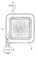
本実施の形態の電荷中和装置は、図1に断面概要図、図2に図1のA−A断面概要図を示すように、図示しないプラズマ発生器から供給されるイオンビームIBを含むビームプラズマPを、ウェハ支持台103に載置された被処理基板であるシリコンウェハ113に照射するもので、シリコンウェハのチャージアップを防止するものである。
Next, an embodiment of the present invention will be described.
(Embodiment 1)
The charge neutralization apparatus according to the present embodiment includes a beam including an ion beam IB supplied from a plasma generator (not shown) as shown in a schematic cross-sectional view in FIG. 1 and a schematic cross-sectional view in FIG. The plasma P is applied to the
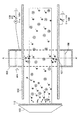
この電荷中和装置は、イオンビームIBの通過経路となる導電チューブ100の所定の位置で、この導電チューブの管軸と垂直な面内で外周を取り囲むように配置されたプラズマチューブ101と、このプラズマチューブ101の外側を取り囲むように配置された導波管102を備え、このプラズマチューブ101内で電子プラズマを生成し、この電子プラズマによってイオンビームIBを取り巻くビームプラズマPの電子不足を同時進行的に補うことによりチャージアップを防止するように構成されている。
The charge neutralization device includes a
この装置では、マイクロ波発生手段としてのマグネトロン104から導波管102を介してプラズマチューブ101内にマイクロ波を導入するとともにプラズマチューブ101内にガスを供給することにより、プラズマチューブ101内に電子プラズマを発生させ、イオンビームIBで構成される系内に電子不足が発生し、+にチャージアップされると、プラズマチューブ101の内壁に設けられた開口部107を介して、電子(プラズマ)を供給し、イオンビームIBの電荷が中和される。
In this apparatus, a microwave is introduced into a
ここでマグネトロン104から導波管102を伝搬してきたマイクロ波は、導波管102とプラズマチューブ101との当接面に設けられたスリット106を介してプラズマチューブ内に導入され、プラズマチューブ101のプラズマ流に対して下流側に設けられたガス供給口105から供給されたガスをイオン化し、電子プラズマを生成する。
Here, the microwave propagating from the
そしてプラズマチューブ101内の電子は、内側の導電チューブ内に開口する開口部107を介してビームプラズマPに供給される。
The electrons in the
この導電チューブ100表面の電位Vcは第1の電源109によって0〜10Vに可変である。
この導波管102表面の電位Vgは第2の電源108によって0〜100Vに可変である。
そしてイオンビームP系内に電子不足が発生すると、瞬時にそれを補うべくプラズマチューブ101から電子が流入する。
この電子の流入量はVcとVgを調整することによって調整可能である。
このように、電子はビームプラズマ中でわずかでも少なくなると、瞬時に開口部107を介してビームプラズマ中に供給されるように構成されている。
The potential Vc on the surface of the
The potential Vg on the surface of the
Then, when an electron shortage occurs in the ion beam P system, electrons flow from the
This inflow amount of electrons can be adjusted by adjusting Vc and Vg.
In this way, the electron is configured to be instantaneously supplied into the beam plasma through the
次に、この電荷中和装置を用い、ゲート酸化膜の形成されたシリコンウェハ表面に、ゲート電極をマスクとしてイオン注入を行うイオン注入方法について説明する。
まず、基板支持台103に被処理基板113として、ゲート酸化膜およびゲート電極を形成したシリコンウェハを載置する。
そして、イオンビームを含むビームプラズマPをこのシリコンウェハ上に照射する。このときビームプラズマはウェハチャージングが発生しない安定した定常状態では、正のイオンと、負の電子との間で電荷のほぼ中和状態が保たれる(Plasma nuetralityと言う)。
Next, an ion implantation method will be described in which ion implantation is performed on the surface of a silicon wafer on which a gate oxide film is formed using this charge neutralization apparatus with a gate electrode as a mask.
First, a silicon wafer on which a gate oxide film and a gate electrode are formed is placed on the
The silicon wafer is irradiated with a beam plasma P including an ion beam. At this time, in a stable steady state in which wafer charging does not occur, the beam plasma maintains a substantially neutralized state of charge between positive ions and negative electrons (referred to as plasma nuetrality).
しかしながら、この例のようにシリコンウェハ上にFETのような絶縁性膜を備えたデバイスが形成され、表面にゲート酸化膜のような絶縁性膜を有する場合、イオンビームによって運ばれる電荷によってチャージングと呼ばれる現象を引き起こす。
このように、ウェハ上のチャージングが絶縁性膜の耐圧限界を超えるとデバイスが破壊されるため、それを防ぐためにウェハ上の正電荷を負の電子電荷によって中和されることが必要になる。
However, when a device having an insulating film such as an FET is formed on a silicon wafer as in this example, and an insulating film such as a gate oxide film is formed on the surface, charging is performed by the charge carried by the ion beam. Cause a phenomenon called
Thus, since the device is destroyed when the charging on the wafer exceeds the withstand voltage limit of the insulating film, the positive charge on the wafer needs to be neutralized by the negative electronic charge to prevent it. .
その際、電子のエネルギーが高いと電子による負のチャージングによってやはりデバイスが静電破壊を起こしてしまうため、電子のエネルギーはデバイスの耐圧限界より低くなければならない。 At that time, if the energy of the electrons is high, the device will also be electrostatically damaged due to negative charging by the electrons, so the energy of the electrons must be lower than the breakdown voltage limit of the device.
例えば、膜厚1nmのゲート絶縁膜の場合耐圧限界は約1V以下である。
シリコンウェハにビームによる正のチャージングが起こると、先ず近傍のビームプラズマ中に存在する低エネルギーのプラズマ電子がウェハ上の正電荷部位に流れ込み、チャージを中和する。
For example, in the case of a gate insulating film having a thickness of 1 nm, the withstand voltage limit is about 1 V or less.
When positive charging due to the beam occurs in the silicon wafer, first, low-energy plasma electrons existing in the nearby beam plasma flow into the positively charged portion on the wafer to neutralize the charge.
これによってビームプラズマの電荷中和状態が崩され、正に偏る。
そしてこの状態がさらに進むとビームプラズマが壊れてビーム中の電位が極めて高くなり、ウェハ上のチャージング破壊が進行して、ビームも自身の正電荷によって発散してしまい、イオン注入は不可能になる。
As a result, the charge neutralization state of the beam plasma is disrupted and biased positively.
If this state further progresses, the beam plasma breaks, the potential in the beam becomes extremely high, charging breakdown on the wafer progresses, the beam also diverges due to its own positive charge, and ion implantation becomes impossible Become.
そこでこの状態を避けるため、正のチャージングが生じるとプラズマチューブから低エネルギーの電子が同時進行的にビームプラズマ系内に供給されることによって、ウェハのチャージングを防止すると共に、ビームプラズマの中和状態を常に保ち、安定で、デバイス収率の高いイオン注入プロセスを維持することになる。 Therefore, in order to avoid this state, when positive charging occurs, low-energy electrons are simultaneously supplied from the plasma tube into the beam plasma system, thereby preventing the wafer from being charged and in the beam plasma. It will maintain a consistent state and maintain a stable, high device yield ion implantation process.
その際、ウェハへの電子流の総和をデバイスやプロセスの条件によって制御することができるため、いくつかのコントロールパラメータを使うことが出来る。 At that time, since the total sum of electron currents to the wafer can be controlled by device and process conditions, several control parameters can be used.
その一つは導電チューブ上に印加する負電圧で、電圧をより負にすることによってウェハへの電子流を増やす。 One is a negative voltage applied on the conductive tube, which increases the electron flow to the wafer by making the voltage more negative.
一つはプラズマチューブ自体、もしくはプラズマチューブ内に浮かした導体に印加する負電圧で、電圧をより負にすることによってウェハへの電子流を増やす。 One is a negative voltage applied to the plasma tube itself or a conductor floating in the plasma tube, and the electron flow to the wafer is increased by making the voltage more negative.
また、一つは導波管中を伝播させるマイクロ波の強度で、強度を上げることによってプラズマチューブ内のプラズマ密度を上げ、電子の絶対量を増やす。 One is the intensity of the microwave propagating in the waveguide. By increasing the intensity, the plasma density in the plasma tube is increased and the absolute amount of electrons is increased.
このように、本発明によれば、ビームプラズマ中で電子が被処理基板(ウェハ)113上に引き寄せられて、電子が不足した状態になると、プラズマチューブから低エネルギーの電子が同時進行的にビームプラズマ系内に供給されることによって、ウェハのチャージングを防止すると共に、常にビームプラズマの中和状態を保ち、安定で、デバイス収率の高いイオン注入プロセスを維持することができる。 As described above, according to the present invention, when electrons are attracted onto the substrate (wafer) 113 to be processed in the beam plasma and the electrons become insufficient, low-energy electrons are simultaneously beamed from the plasma tube. By being supplied into the plasma system, it is possible to prevent the wafer from being charged and to maintain a neutral state of the beam plasma at all times, thereby maintaining a stable and high device yield ion implantation process.
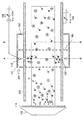
(実施の形態2)
前記実施の形態1では、導電チューブの管軸と垂直な面内で外周を取り囲むように配置されたプラズマチューブ101と、このプラズマチューブ101の外側を取り囲むように配置された導波管102を備え、このプラズマチューブ101内で電子プラズマを生成するものについて説明したが、本実施の形態の電荷中和装置は、図3に断面概要図、図4および図5に図3のA−A断面概要図およびB−B断面図を示す。本実施の形態では、基本的には導電チューブ100を囲むようにプラズマチューブ101と導波管102とが並置された点で前記実施の形態1と異なる。この例では進行波によるプラズマ励起を行っている。
(Embodiment 2)
In the first embodiment, the
またこの場合バイアスを調整するための電位はプラズマチューブ101内に配設されたバイアスワイヤ110を介して第2の電源108から供給される。
他については基本的には実施の形態1と同様に形成されている。
In this case, a potential for adjusting the bias is supplied from the
Others are basically the same as in the first embodiment.
この場合についても図8に示したようなシリコンウェハにソースドレイン形成のためのイオン注入を行った場合にもチャージアップが抑制され、効率よくイオン注入がなされることから、1nm程度の薄いゲート絶縁膜をもつFETの場合にも絶縁破壊が抑制され2eV以下の耐圧のFETに対しても絶縁破壊なしに高歩留まりでFETを得る事が可能となる。 In this case as well, when ion implantation for source / drain formation is performed on a silicon wafer as shown in FIG. 8, charge-up is suppressed and ion implantation is performed efficiently. In the case of an FET having a film, dielectric breakdown is suppressed, and an FET having a breakdown voltage of 2 eV or less can be obtained at a high yield without dielectric breakdown.
この電荷中和装置は、イオンビームIBの通過経路となる導電チューブ100の所定の位置で、この導電チューブの管軸と垂直な面内で外周を取り囲むように配置されたプラズマチューブ101と、このプラズマチューブ101の外側を取り囲むように配置された導波管102を備え、このプラズマチューブ101内で電子プラズマを生成し、この電子プラズマによってイオンビームIBを取り巻くビームプラズマPの電子不足を同時進行的に補うことによりチャージアップを防止するように構成されている。
The charge neutralization device includes a
この装置では、マイクロ波発生手段としてのマグネトロン104から導波管102を介してプラズマチューブ101内にマイクロ波を導入するとともにプラズマチューブ101内にガスを供給することにより、プラズマチューブ101内に電子プラズマを発生させ、イオンビームIBで構成される系内に電子不足が発生し、+にチャージアップされると、プラズマチューブ101の内壁に設けられた開口部107を介して、電子(プラズマ)を供給し、イオンビームIBの電荷が中和される。
In this apparatus, a microwave is introduced into a
ここでマグネトロン104から導波管102を伝搬してきたマイクロ波は、導波管102とプラズマチューブ101との当接面に設けられたスリット106を介してプラズマチューブ内に導入され、プラズマチューブ101のプラズマ流に対して下流側に設けられたガス供給口105から供給されたガスをイオン化し、電子プラズマを生成する。
Here, the microwave propagating from the
(実施の形態3)
前記実施の形態2では、進行波によるプラズマ励起を行う例について説明したが、定在波を用いる場合も有効である。
この場合、図6にビームに垂直方向の断面図を示すように導波管102が定在波を形成し得るように閉管構造をとる点が異なるのみで他は前記実施の形態2と同様である。
ビームに平行な方向の断面図は図3に示したものと同様である。
本実施の形態では、基本的には導電チューブ100を囲むようにプラズマチューブ101と導波管102とが並置され、定在波によるプラズマ励起を行っている。
(Embodiment 3)
In the second embodiment, an example of performing plasma excitation by traveling waves has been described. However, it is also effective to use standing waves.
In this case, as shown in the sectional view in the direction perpendicular to the beam in FIG. 6, the only difference is that the
The cross-sectional view in the direction parallel to the beam is the same as that shown in FIG.
In the present embodiment, basically, the
(実施の形態4)
本実施の形態では、図7に示すように、カスプ磁場を生成するカスプマグネット110Cをプラズマチューブ102の側面に配設したことを特徴とするものである。カスプマグネット110Cはプラズマチューブ102の側面の両側でも良いし片側でもよい。
この場合も、図7にビームに垂直方向の断面図を示すようにカスプマグネットを配設した点が異なるのみで他は前記実施の形態2と同様である。
ビームに平行な方向の断面図は図3に示したものと同様である。
(Embodiment 4)
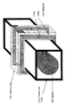
In the present embodiment, as shown in FIG. 7, a
Also in this case, the second embodiment is the same as the second embodiment except that a cusp magnet is provided as shown in a sectional view perpendicular to the beam in FIG.
The cross-sectional view in the direction parallel to the beam is the same as that shown in FIG.
具体的には、プラズマチューブを構成する導波管102の側面に交互に所定の間隔で磁場方向を逆にした磁石を配設し、プラズマチューブ101内にカスプ磁場を生じさせる。そして、このカスプ磁場に起因した磁気勾配及びこれによってもたらされる磁気力によって、低エネルギーの電子をプラズマチューブ内に高密度に閉じ込めるようにしたものである。
Specifically, magnets whose magnetic field directions are reversed at predetermined intervals are alternately arranged on the side surfaces of the
なおここで用いるカスプ磁場は磁場強度自体が500ガウス以下の弱い磁場であるため、ECRポイントはおのずから外れることになるため、問題はないが、本発明ではプラズマ密度を高くしつつ電子エネルギー密度をために、ECR条件をはずすように磁場強度を設定する必要がある。
本実施の形態では、基本的には導電チューブ100を囲むようにプラズマチューブ101と導波管102とが並置され、定在波によるプラズマ励起を行っている。
Note that the cusp magnetic field used here is a weak magnetic field with a magnetic field intensity of 500 gauss or less, so the ECR point is not natural, so there is no problem. In addition, it is necessary to set the magnetic field strength so as to remove the ECR condition.
In the present embodiment, basically, the
(実施の形態5)
前記実施の形態4では、カスプマグネット120をプラズマチューブ102の側面に配設したが、本実施の形態では、カスプマグネッ120をプラズマチューブ102の外周面上に配設したことを特徴とする。
すなわち本実施の形態では、図8に示すように、カスプ磁場を生成するカスプマグネット120をプラズマチューブ102の外周面上に配設したことを特徴とするものである。
この場合も、図8にビームに垂直方向の断面図を示すようにカスプマグネットを配設した点が異なるのみで他は前記実施の形態2と同様である。
ビームに平行な方向の断面図は図3に示したものと同様である。
(Embodiment 5)
In the fourth embodiment, the
That is, the present embodiment is characterized in that a
Also in this case, the second embodiment is the same as the second embodiment except that a cusp magnet is provided as shown in a sectional view perpendicular to the beam in FIG.
The cross-sectional view in the direction parallel to the beam is the same as that shown in FIG.
具体的には、プラズマチューブを構成する導波管102の外周面に交互に所定の間隔で磁場方向を逆にした磁石を配設し、プラズマチューブ101内にカスプ磁場を生じさせる。そして、このカスプ磁場に起因した磁気勾配及びこれによってもたらされる磁気力によって、低エネルギーの電子をプラズマチューブ内に高密度に閉じ込めるようにしたものである。
Specifically, magnets whose magnetic field directions are reversed at predetermined intervals are alternately arranged on the outer peripheral surface of the
(実施の形態6)
前記実施の形態4,5では、カスプマグネット110C、または120をプラズマチューブ102の側面または外周面に配設したが、本実施の形態では、カスプマグネット130を内側と外側とで、プラズマチューブ102をはさむように配設したことを特徴とする。
すなわち本実施の形態では、図9に示すように、カスプ磁場を生成するカスプマグネット130をプラズマチューブ102の内周面と外周面上とに配設したことを特徴とするものである。
この場合も、図9に斜視図を示すようにカスプマグネットを配設した位置が異なるのみで他は前記実施の形態2と同様である。
ビームに平行な方向の断面図は図3に示したものと同様である。
(Embodiment 6)
In the fourth and fifth embodiments, the
That is, in this embodiment, as shown in FIG. 9,
Also in this case, as shown in the perspective view of FIG. 9, the other points are the same as those of the second embodiment except that the cusp magnets are disposed at different positions.
The cross-sectional view in the direction parallel to the beam is the same as that shown in FIG.
具体的には、プラズマチューブを構成する導波管102の内周および外周面に交互に所定の間隔で磁場方向を逆にした磁石を配設し、プラズマチューブ101内にカスプ磁場を生じさせる。そして、このカスプ磁場に起因した磁気勾配及びこれによってもたらされる磁気力によって、低エネルギーの電子をプラズマチューブ内に高密度に閉じ込めるようにしたものである。
Specifically, magnets whose magnetic field directions are alternately reversed at predetermined intervals are disposed on the inner and outer peripheral surfaces of the
前記実施の形態1乃至6では導波管を用いたプラズマ発生装置について説明したが、導波管に限定されることなく同軸ケーブルを用いてプラズマ励起を行うようなものについても適用可能である。 In the first to sixth embodiments, the plasma generator using the waveguide has been described. However, the present invention is not limited to the waveguide, but can be applied to a device that performs plasma excitation using a coaxial cable.
本発明は、低エネルギーの電子を効率良く均一に供給してイオン注入によるチャージアップと電子によるダメージ、低エネルギーイオンビームの空間電荷を効果的に中和することができ、大面積の基板に対応可能な電荷中和器を提供できるので有効である。 The present invention can efficiently and uniformly supply low-energy electrons to effectively neutralize charge-up and damage caused by ion implantation and space charge of a low-energy ion beam. This is effective because a possible charge neutralizer can be provided.
Claims (17)
マイクロ波発生手段と、
前記マイクロ波発生手段で発生せしめられたマイクロ波によって電子プラズマを発生するプラズマ生成手段と、
前記プラズマ生成手段で生成された電子プラズマを、イオンビームを含むビームプラズマ領域に対し、前記イオンビームを取り囲むプラズマチューブを介して、接触させる接触手段とを備え、
前記プラズマチューブ内に配置されたバイアスワイヤを介して電源から、バイアスを制御するための電位が、供給され、
イオンビームに供給される電子プラズマ量を制御するように構成され、
前記プラズマチューブは、イオンビームをリング状に取り囲み、
前記プラズマ生成手段は、前記プラズマチューブの外側を取り囲むように配置された導波管を備え、前記マイクロ波発生手段から前記導波管を介して前記プラズマチューブ内にマイクロ波を導入するとともに前記プラズマチューブ内にガスを供給することにより、前記プラズマチューブ内にプラズマを発生させ、
前記導波管は、前記導波管中のマイクロ波の伝搬方向が、前記イオンビームの流れ方向に直交する面で、前記イオンビームを囲むように配設され、
前記導波管は、前記導波管中のマイクロ波伝搬方向の下流側から上流側に向かって前記プラズマチューブへのガスの供給がなされるように構成された電荷中和装置。A charge neutralizer,
Microwave generation means;
Plasma generating means for generating electron plasma by microwaves generated by the microwave generating means;
Contact means for bringing the electron plasma generated by the plasma generation means into contact with a beam plasma region including an ion beam through a plasma tube surrounding the ion beam;
A potential for controlling the bias is supplied from a power source via a bias wire arranged in the plasma tube,
Configured to control the amount of electron plasma supplied to the ion beam ;
The plasma tube surrounds the ion beam in a ring shape,
The plasma generation means includes a waveguide arranged so as to surround the outside of the plasma tube, and introduces microwaves into the plasma tube from the microwave generation means via the waveguide and the plasma. By supplying gas into the tube, plasma is generated in the plasma tube,
The waveguide is disposed so that the propagation direction of the microwave in the waveguide surrounds the ion beam in a plane orthogonal to the flow direction of the ion beam,
The said waveguide is a charge neutralization apparatus comprised so that supply of the gas to the said plasma tube may be made from the downstream of the microwave propagation direction in the said waveguide toward the upstream .
マイクロ波発生手段と、 Microwave generation means;
前記マイクロ波発生手段で発生せしめられたマイクロ波によって電子プラズマを発生するプラズマ生成手段と、 Plasma generating means for generating electron plasma by microwaves generated by the microwave generating means;
前記プラズマ生成手段で生成された電子プラズマを、イオンビームを含むビームプラズマ領域に対し、前記イオンビームを取り囲むプラズマチューブを介して、接触させる接触手段とを備え、 Contact means for bringing the electron plasma generated by the plasma generation means into contact with a beam plasma region including an ion beam through a plasma tube surrounding the ion beam;
前記プラズマチューブ内に配置されたバイアスワイヤを介して電源から、バイアスを制御するための電位が、供給され、 A potential for controlling the bias is supplied from a power source via a bias wire arranged in the plasma tube,
イオンビームに供給される電子プラズマ量を制御するように構成され、 Configured to control the amount of electron plasma supplied to the ion beam;
マイクロ波励起を用いて低温プラズマを維持し、それによって2eV以下の低エネルギーの電子を供給する電荷中和装置。 A charge neutralization device that maintains a low temperature plasma using microwave excitation and thereby supplies electrons of low energy below 2 eV.
前記プラズマチューブは、イオンビームをリング状に取り囲む電荷中和装置。The charge neutralization device according to claim 2 ,
The plasma tube is a charge neutralization device that surrounds an ion beam in a ring shape.
前記接触手段は、前記イオンビームの形状もしくは前記イオンビームのスキャンエリアに対応して、前記イオンビームもしくは前記スキャンエリアの外周を取り囲むように配置されたプラズマチューブを含むことを特徴とする電荷中和装置。The charge neutralization device according to claim 2 ,
The contact means includes a plasma tube arranged so as to surround an outer periphery of the ion beam or the scan area corresponding to a shape of the ion beam or a scan area of the ion beam. apparatus.
前記プラズマ生成手段は、前記プラズマチューブの外側を取り囲むように配置された導波管を備え、前記マイクロ波発生手段から前記導波管を介して前記プラズマチューブ内にマイクロ波を導入するとともに前記プラズマチューブ内にガスを供給することにより、前記プラズマチューブ内にプラズマを発生させることを特徴とする電荷中和装置。The charge neutralization device according to claim 3 or 4 ,
The plasma generation means includes a waveguide arranged so as to surround the outside of the plasma tube, and introduces microwaves into the plasma tube from the microwave generation means via the waveguide and the plasma. A charge neutralizing apparatus, wherein plasma is generated in the plasma tube by supplying a gas into the tube.
前記導波管は、前記導波管中のマイクロ波の伝搬方向が、前記イオンビームの流れ方向に直交する面で、前記イオンビームを囲むように配設されたことを特徴とする電荷中和装置。The charge neutralization device according to claim 5 ,
The waveguide is arranged so that the propagation direction of the microwave in the waveguide is surrounded by the surface orthogonal to the flow direction of the ion beam so as to surround the ion beam. apparatus.
前記導波管は、前記導波管中のマイクロ波伝搬方向の下流側から上流側に向かって前記プラズマチューブへのガスの供給がなされるように構成されたことを特徴とする電荷中和装置。The charge neutralization device according to claim 6 ,
The charge neutralizing apparatus, wherein the waveguide is configured such that gas is supplied to the plasma tube from the downstream side to the upstream side in the microwave propagation direction in the waveguide. .
前記プラズマ生成手段は、同軸ケーブルであることを特徴とする電荷中和装置。The charge neutralization device according to any one of claims 1 and 5 to 7 ,
The plasma neutralizing device is a charge neutralizing device, characterized in that it is a coaxial cable.
前記ガスは不活性ガスであることを特徴とする電荷中和装置。The charge neutralization device according to any one of claims 1 and 5 to 8 ,
The charge neutralizing apparatus, wherein the gas is an inert gas.
前記プラズマチューブと前記導波管との間にはそれぞれ位置をあわせた少なくともひとつのスリットを有することを特徴とする電荷中和装置。The charge neutralization device according to any one of claims 1 and 5 to 9 ,
An electric charge neutralization apparatus comprising at least one slit aligned between the plasma tube and the waveguide.
前記プラズマチューブと前記導波管との間にはそれぞれ位置をあわせた複数のスリットを有することを特徴とする電荷中和装置。The charge neutralization device according to claim 10 ,
A charge neutralizing apparatus comprising a plurality of slits aligned with each other between the plasma tube and the waveguide.
前記プラズマチューブの前記イオンビームに近接する側にひとつの開口部を有することを特徴とする電荷中和装置。The charge neutralization device according to any one of claims 1 and 3 to 11 ,
An electric charge neutralization device having one opening on a side of the plasma tube close to the ion beam.
前記プラズマチューブの前記イオンビームに近接する側に複数の開口部を有することを特徴とする電荷中和装置。The charge neutralization device according to any one of claims 1 and 3 to 12 ,
A charge neutralizing apparatus comprising a plurality of openings on a side of the plasma tube close to the ion beam.
マイクロ波励起を用いてプラズマを発生させて、前記イオンビームを含むビームプラズマ中に電子を供給することを特徴とする電荷中和装置。The charge neutralization device according to any one of claims 1 to 13 ,
A charge neutralization apparatus, wherein plasma is generated using microwave excitation and electrons are supplied into a beam plasma including the ion beam.
マイクロ波励起を用いてプラズマを発生させて、前記イオンビームを照射する固体基体近傍の少なくとも1つに電子を供給することを特徴とする電荷中和装置。The charge neutralization device according to any one of claims 1 to 13 ,
A charge neutralization apparatus characterized in that plasma is generated using microwave excitation and electrons are supplied to at least one of the solid bases near which the ion beam is irradiated.
Priority Applications (1)
| Application Number | Priority Date | Filing Date | Title |
|---|---|---|---|
| JP2006513892A JP5046641B2 (en) | 2004-05-25 | 2005-05-24 | Charge neutralizer |
Applications Claiming Priority (4)
| Application Number | Priority Date | Filing Date | Title |
|---|---|---|---|
| JP2004183112 | 2004-05-25 | ||
| JP2004183112 | 2004-05-25 | ||
| PCT/JP2005/009460 WO2005117059A1 (en) | 2004-05-25 | 2005-05-24 | Charge neutralization device |
| JP2006513892A JP5046641B2 (en) | 2004-05-25 | 2005-05-24 | Charge neutralizer |
Publications (2)
| Publication Number | Publication Date |
|---|---|
| JPWO2005117059A1 JPWO2005117059A1 (en) | 2008-04-03 |
| JP5046641B2 true JP5046641B2 (en) | 2012-10-10 |
Family
ID=35451128
Family Applications (1)
| Application Number | Title | Priority Date | Filing Date |
|---|---|---|---|
| JP2006513892A Expired - Fee Related JP5046641B2 (en) | 2004-05-25 | 2005-05-24 | Charge neutralizer |
Country Status (7)
| Country | Link |
|---|---|
| US (1) | US7557364B2 (en) |
| EP (1) | EP1753009A4 (en) |
| JP (1) | JP5046641B2 (en) |
| KR (1) | KR101148048B1 (en) |
| CN (1) | CN1969365B (en) |
| TW (1) | TW200603195A (en) |
| WO (1) | WO2005117059A1 (en) |
Families Citing this family (11)
| Publication number | Priority date | Publication date | Assignee | Title |
|---|---|---|---|---|
| JP5046641B2 (en) * | 2004-05-25 | 2012-10-10 | パナソニック株式会社 | Charge neutralizer |
| GB2440414B (en) * | 2006-07-12 | 2010-10-27 | Applied Materials Inc | An ion beam guide tube |
| EP2086285A1 (en) * | 2008-02-01 | 2009-08-05 | Anton Paar GmbH | Applicator and Apparatus for heating samples by microwave radiation |
| US9053907B2 (en) * | 2012-04-04 | 2015-06-09 | Taiwan Semiconductor Manufacturing Co., Ltd. | System and method of ion neutralization with multiple-zoned plasma flood gun |
| TWI508127B (en) * | 2012-11-13 | 2015-11-11 | E G Electro Graph Inc | Magnetic field reduction apparatus and magnetic plasma flood system for ion beam processing |
| US8933630B2 (en) * | 2012-12-19 | 2015-01-13 | Taiwan Semiconductor Manufacturing Co., Ltd. | Arc chamber with multiple cathodes for an ion source |
| DE102016005537A1 (en) * | 2016-05-04 | 2017-11-09 | Forschungszentrum Jülich GmbH Fachbereich Patente | Method for producing layers of ReRAM memories and use of an implanter |
| EP3389078A1 (en) * | 2017-04-13 | 2018-10-17 | The Swatch Group Research and Development Ltd | Method for implanting multi-charged ions on a surface of an object to be treated and installation for implementing said method |
| CN112885689A (en) * | 2021-03-11 | 2021-06-01 | 无锡中微掩模电子有限公司 | Novel FEI850 ion beam repairing machine electron neutralization funnel |
| CN115376873A (en) * | 2021-05-18 | 2022-11-22 | 江苏鲁汶仪器有限公司 | Ion source device, use method thereof and vacuum processing system |
| KR102857355B1 (en) | 2022-11-16 | 2025-09-09 | 주식회사 인포비온 | Electron emitting source |
Citations (7)
| Publication number | Priority date | Publication date | Assignee | Title |
|---|---|---|---|---|
| JPS61283116A (en) * | 1985-05-15 | 1986-12-13 | エナ−ジ−・コンバ−シヨン・デバイセス・インコ−ポレ−テツド | Improved microwave system and method for manufacture of semiconductor member and improved semiconductor member to bemanufactured thereby |
| JPH05290790A (en) * | 1992-04-16 | 1993-11-05 | Hitachi Ltd | Ion implanter |
| JPH0688225A (en) * | 1992-09-10 | 1994-03-29 | Hitachi Ltd | Ion irradiation device and antistatic device |
| JPH06283131A (en) * | 1993-03-29 | 1994-10-07 | Shimadzu Corp | Ion beam equipment |
| JPH06283121A (en) * | 1991-06-12 | 1994-10-07 | Japan Atom Energy Res Inst | Microwave ion source |
| JP2002352761A (en) * | 2001-05-28 | 2002-12-06 | Nissin Electric Co Ltd | Ion beam irradiation device |
| JP2004131759A (en) * | 2002-10-08 | 2004-04-30 | Canon Inc | Deposition film formation method |
Family Cites Families (19)
| Publication number | Priority date | Publication date | Assignee | Title |
|---|---|---|---|---|
| US2628311A (en) * | 1948-11-04 | 1953-02-10 | Rca Corp | Multiple slot antenna |
| US3729740A (en) * | 1971-01-20 | 1973-04-24 | Sumitomo Electric Industries | Vehicle antenna for vehicular communication system using leaky coaxial cable |
| US4885839A (en) * | 1985-05-30 | 1989-12-12 | General Signal Corporation | Process of fabricating a waveguide |
| US4886971A (en) * | 1987-03-13 | 1989-12-12 | Mitsubishi Denki Kabushiki Kaisha | Ion beam irradiating apparatus including ion neutralizer |
| JPH0821361B2 (en) | 1989-10-20 | 1996-03-04 | 三菱電機株式会社 | Ion implanter and charge neutralizer |
| US5270724A (en) * | 1991-04-04 | 1993-12-14 | Hughes Aircraft Company | Multifrequency phased array aperture |
| FR2689717B1 (en) * | 1992-04-03 | 1994-05-13 | Commissariat A Energie Atomique | MICROWAVE APPLICATION DEVICE AND PLASMA REACTOR USING THE SAME. |
| JP3054302B2 (en) * | 1992-12-02 | 2000-06-19 | アプライド マテリアルズ インコーポレイテッド | Plasma emission system to reduce charging on semiconductor wafers during ion implantation |
| DE19600223A1 (en) * | 1996-01-05 | 1997-07-17 | Ralf Dr Dipl Phys Spitzl | Device for generating plasmas using microwaves |
| JP3284918B2 (en) * | 1997-04-11 | 2002-05-27 | 株式会社日立製作所 | Antistatic method and ion implanter |
| GB9710380D0 (en) * | 1997-05-20 | 1997-07-16 | Applied Materials Inc | Electron flood apparatus for neutralising charge build-up on a substrate during ion implantation |
| DE19726663A1 (en) * | 1997-06-23 | 1999-01-28 | Sung Spitzl Hildegard Dr Ing | Device for generating homogeneous microwave plasmas |
| US5856674A (en) * | 1997-09-16 | 1999-01-05 | Eaton Corporation | Filament for ion implanter plasma shower |
| US6359286B1 (en) * | 1998-07-10 | 2002-03-19 | Applied Materials, Inc. | Method and apparatus for neutralizing space charge in an ion beam |
| JP3608416B2 (en) * | 1999-02-02 | 2005-01-12 | 日新電機株式会社 | Plasma source |
| US6512333B2 (en) * | 1999-05-20 | 2003-01-28 | Lee Chen | RF-powered plasma accelerator/homogenizer |
| GB2411763B (en) * | 2004-03-05 | 2009-02-18 | Thermo Electron Corp | Flood gun for charge neutralization |
| US7078712B2 (en) * | 2004-03-18 | 2006-07-18 | Axcelis Technologies, Inc. | In-situ monitoring on an ion implanter |
| JP5046641B2 (en) * | 2004-05-25 | 2012-10-10 | パナソニック株式会社 | Charge neutralizer |
-
2005
- 2005-05-24 JP JP2006513892A patent/JP5046641B2/en not_active Expired - Fee Related
- 2005-05-24 CN CN2005800192956A patent/CN1969365B/en not_active Expired - Fee Related
- 2005-05-24 EP EP05743260A patent/EP1753009A4/en not_active Withdrawn
- 2005-05-24 KR KR1020067024751A patent/KR101148048B1/en not_active Expired - Fee Related
- 2005-05-24 US US11/597,324 patent/US7557364B2/en not_active Expired - Fee Related
- 2005-05-24 WO PCT/JP2005/009460 patent/WO2005117059A1/en not_active Ceased
- 2005-05-25 TW TW094117018A patent/TW200603195A/en not_active IP Right Cessation
Patent Citations (7)
| Publication number | Priority date | Publication date | Assignee | Title |
|---|---|---|---|---|
| JPS61283116A (en) * | 1985-05-15 | 1986-12-13 | エナ−ジ−・コンバ−シヨン・デバイセス・インコ−ポレ−テツド | Improved microwave system and method for manufacture of semiconductor member and improved semiconductor member to bemanufactured thereby |
| JPH06283121A (en) * | 1991-06-12 | 1994-10-07 | Japan Atom Energy Res Inst | Microwave ion source |
| JPH05290790A (en) * | 1992-04-16 | 1993-11-05 | Hitachi Ltd | Ion implanter |
| JPH0688225A (en) * | 1992-09-10 | 1994-03-29 | Hitachi Ltd | Ion irradiation device and antistatic device |
| JPH06283131A (en) * | 1993-03-29 | 1994-10-07 | Shimadzu Corp | Ion beam equipment |
| JP2002352761A (en) * | 2001-05-28 | 2002-12-06 | Nissin Electric Co Ltd | Ion beam irradiation device |
| JP2004131759A (en) * | 2002-10-08 | 2004-04-30 | Canon Inc | Deposition film formation method |
Also Published As
| Publication number | Publication date |
|---|---|
| EP1753009A1 (en) | 2007-02-14 |
| CN1969365B (en) | 2011-02-09 |
| KR20070029177A (en) | 2007-03-13 |
| CN1969365A (en) | 2007-05-23 |
| JPWO2005117059A1 (en) | 2008-04-03 |
| US20070228294A1 (en) | 2007-10-04 |
| TW200603195A (en) | 2006-01-16 |
| EP1753009A4 (en) | 2011-07-06 |
| WO2005117059A1 (en) | 2005-12-08 |
| US7557364B2 (en) | 2009-07-07 |
| KR101148048B1 (en) | 2012-05-25 |
| TWI360148B (en) | 2012-03-11 |
Similar Documents
| Publication | Publication Date | Title |
|---|---|---|
| US6759665B2 (en) | Method and system for ion beam containment in an ion beam guide | |
| US5206516A (en) | Low energy, steered ion beam deposition system having high current at low pressure | |
| US7800083B2 (en) | Plasma electron flood for ion beam implanter | |
| CN1809910B (en) | Thin magnetron structures for plasma generation in ion implantation systems | |
| WO2010120569A2 (en) | Conjugated icp and ecr plasma sources for wide ribbon ion beam generation and control | |
| US8760054B2 (en) | Microwave plasma electron flood | |
| KR101726560B1 (en) | Enhanced low energy ion beam transport in ion implantation | |
| JP5046641B2 (en) | Charge neutralizer | |
| KR102892702B1 (en) | Processing system and extraction assembly including high angle extraction optics | |
| US20130287963A1 (en) | Plasma Potential Modulated ION Implantation Apparatus | |
| TW202036637A (en) | Ion extraction optics and ion extraction processing apparatus | |
| KR100602319B1 (en) | Waveguide for microwave excitation of plasma in an ion beam guide | |
| KR100904313B1 (en) | Contaminant removal system and method for ion beam | |
| WO2005086204A2 (en) | Modulating ion beam current | |
| TWI322451B (en) | Methods and apparatus for ion beam neutralization in magnets | |
| JP2008028360A (en) | Ion implantation equipment using plasma | |
| CN101103432B (en) | Electron injection in ion implanter magnets |
Legal Events
| Date | Code | Title | Description |
|---|---|---|---|
| A621 | Written request for application examination |
Free format text: JAPANESE INTERMEDIATE CODE: A621 Effective date: 20080214 |
|
| A131 | Notification of reasons for refusal |
Free format text: JAPANESE INTERMEDIATE CODE: A131 Effective date: 20110322 |
|
| A521 | Request for written amendment filed |
Free format text: JAPANESE INTERMEDIATE CODE: A523 Effective date: 20110523 |
|
| A131 | Notification of reasons for refusal |
Free format text: JAPANESE INTERMEDIATE CODE: A131 Effective date: 20120221 |
|
| A521 | Request for written amendment filed |
Free format text: JAPANESE INTERMEDIATE CODE: A523 Effective date: 20120420 |
|
| TRDD | Decision of grant or rejection written | ||
| A01 | Written decision to grant a patent or to grant a registration (utility model) |
Free format text: JAPANESE INTERMEDIATE CODE: A01 Effective date: 20120619 |
|
| A01 | Written decision to grant a patent or to grant a registration (utility model) |
Free format text: JAPANESE INTERMEDIATE CODE: A01 |
|
| A61 | First payment of annual fees (during grant procedure) |
Free format text: JAPANESE INTERMEDIATE CODE: A61 Effective date: 20120717 |
|
| FPAY | Renewal fee payment (event date is renewal date of database) |
Free format text: PAYMENT UNTIL: 20150727 Year of fee payment: 3 |
|
| R150 | Certificate of patent or registration of utility model |
Free format text: JAPANESE INTERMEDIATE CODE: R150 |
|
| LAPS | Cancellation because of no payment of annual fees |