JP5034763B2 - Oscillator - Google Patents
Oscillator Download PDFInfo
- Publication number
- JP5034763B2 JP5034763B2 JP2007207516A JP2007207516A JP5034763B2 JP 5034763 B2 JP5034763 B2 JP 5034763B2 JP 2007207516 A JP2007207516 A JP 2007207516A JP 2007207516 A JP2007207516 A JP 2007207516A JP 5034763 B2 JP5034763 B2 JP 5034763B2
- Authority
- JP
- Japan
- Prior art keywords
- vibrator
- terminal
- inductor
- value
- resistance
- Prior art date
- Legal status (The legal status is an assumption and is not a legal conclusion. Google has not performed a legal analysis and makes no representation as to the accuracy of the status listed.)
- Expired - Fee Related
Links
Images


Description
本発明は、振動子を用いた発振器に関する。 The present invention relates to an oscillator using a vibrator.
SAW(Surface Acoustic Wave、弾性表面波)振動子、音叉型振動子、AT振動子などの水晶振動子110を用いた発振器1は、例えば図5(A)に示すような回路で構成されている(非特許文献1の図2参照)。また、水晶振動子110の等価回路111は、図5(B)に示すように直列に接続された等価直列インダクタL1と等価直列コンデンサC1と等価直列抵抗R1と、これらと平行に接続された等価並列コンデンサC0とからなる回路で表現される(非特許文献1の図1参照)。水晶振動子の品質係数であるQ特性Q1は、角周波数をωとすると、Q1=ω×L1/R1のように算出され、発振起動時間td1は、td1=(2×Q1)/ωのように算出される。
An
しかしながら、水晶振動子110は、Q特性を高く設定すると発振の周波数純度を高くすることができるが、発振の起動時間が遅くなるという問題がある。
However, although the
本発明は、上述の課題を解決するためになされたものであり、以下の形態又は適用例として実現することが可能である。 The present invention has been made to solve the above-described problems, and can be realized as the following forms or application examples.
[適用例1]
第1の端子と、第2の端子と、前記第1の端子と前記第2の端子との間に、直列に接続された抵抗素子及びインダクタと、前記抵抗素子と並列に接続された振動子と、前記第1の端子と前記第2の端子との間に接続されたコンデンサと、前記第1の端子と前記第2の端子との間に接続され、前記振動子を振動させる発振回路部と、を含み、前記インダクタの値と前記抵抗素子の抵抗値と前記振動子の等価直列インダクタの値と前記振動子の等価直列抵抗の抵抗値とは、(前記インダクタの値÷前記抵抗素子の抵抗値)<(前記振動子の等価直列インダクタの値÷前記振動子の等価直列抵抗の抵抗値)の関係を満たす、ことを特徴とする発振器。
[Application Example 1]
A first element, a second terminal, a resistance element and an inductor connected in series between the first terminal and the second terminal, and a vibrator connected in parallel with the resistance element And a capacitor connected between the first terminal and the second terminal, and an oscillation circuit unit connected between the first terminal and the second terminal to vibrate the vibrator The value of the inductor, the resistance value of the resistance element, the value of the equivalent series inductor of the vibrator, and the resistance value of the equivalent series resistance of the vibrator are (the value of the inductor / the resistance element) Resistance value) <(value of equivalent series inductor of the vibrator / resistance value of equivalent series resistance of the vibrator).
この構成によれば、振動子が発振を開始するまでの期間にインダクタとコンデンサにより構成されるLC並列発振回路が先に発振をするので振動子単体より短時間で起動することができ、振動子が発振を開始すれば周波数純度の高い発振器を実現できる。 According to this configuration, since the LC parallel oscillation circuit composed of the inductor and the capacitor first oscillates until the vibrator starts oscillating, the vibrator can be started in a shorter time than the vibrator alone. If oscillation starts, an oscillator with high frequency purity can be realized.
[適用例2]
第1の端子と、第2の端子と、前記第1の端子と前記第2の端子との間に、直列に接続された抵抗素子及びコンデンサと、前記抵抗素子と並列に接続された振動子と、前記第1の端子と前記第2の端子との間に接続されたインダクタと、前記第1の端子と前記第2の端子との間に接続され、前記振動子を振動させる発振回路部と、を含み、前記インダクタの値と前記抵抗素子の抵抗値と前記振動子の等価直列インダクタの値と前記振動子の等価直列抵抗の抵抗値とは、(前記インダクタの値÷前記抵抗素子の抵抗値)<(前記振動子の等価直列インダクタの値÷前記振動子の等価直列抵抗の抵抗値)の関係を満たす、ことを特徴とする発振器。
[Application Example 2]
A first element, a second terminal, a resistance element and a capacitor connected in series between the first terminal and the second terminal, and a vibrator connected in parallel with the resistance element An inductor connected between the first terminal and the second terminal, and an oscillation circuit unit connected between the first terminal and the second terminal to vibrate the vibrator The value of the inductor, the resistance value of the resistance element, the value of the equivalent series inductor of the vibrator, and the resistance value of the equivalent series resistance of the vibrator are (the value of the inductor / the resistance element) Resistance value) <(value of equivalent series inductor of the vibrator / resistance value of equivalent series resistance of the vibrator).
この構成によれば、振動子が発振を開始するまでの期間にインダクタとコンデンサにより構成されるLC並列発振回路が先に発振をするので振動子単体より短時間で起動することができ、振動子が発振を開始すれば周波数純度の高い発振器を実現できる。 According to this configuration, since the LC parallel oscillation circuit composed of the inductor and the capacitor first oscillates until the vibrator starts oscillating, the vibrator can be started in a shorter time than the vibrator alone. If oscillation starts, an oscillator with high frequency purity can be realized.
[適用例3]
上記に記載の発振器において、前記振動子の等価直列抵抗の抵抗値は前記抵抗素子の抵抗値より小さいことを特徴とする発振器。
[Application Example 3]
The oscillator according to the above, wherein a resistance value of an equivalent series resistance of the vibrator is smaller than a resistance value of the resistance element.
この構成によれば、振動子が発振を開始するまでの期間にインダクタとコンデンサにより構成されるLC並列発振回路が先に発振をするので振動子単体より短時間で起動することができ、振動子が発振を開始すれば周波数純度の高い発振器を実現できる。 According to this configuration, since the LC parallel oscillation circuit composed of the inductor and the capacitor first oscillates until the vibrator starts oscillating, the vibrator can be started in a shorter time than the vibrator alone. If oscillation starts, an oscillator with high frequency purity can be realized.
[適用例4]
上記に記載の発振器において、前記インダクタの値は前記振動子の等価直列インダクタの値より小さいことを特徴とする発振器。
[Application Example 4]
The oscillator according to the above, wherein the value of the inductor is smaller than the value of the equivalent series inductor of the vibrator.
この構成によれば、振動子が発振を開始するまでの期間にインダクタとコンデンサにより構成されるLC並列発振回路が先に発振をするので振動子単体より短時間で起動することができ、振動子が発振を開始すれば周波数純度の高い発振器を実現できる。 According to this configuration, since the LC parallel oscillation circuit composed of the inductor and the capacitor first oscillates until the vibrator starts oscillating, the vibrator can be started in a shorter time than the vibrator alone. If oscillation starts, an oscillator with high frequency purity can be realized.
[適用例5]
上記に記載の発振器において、前記発振回路部は、前記第1の端子と前記第2の端子との間に差動接続された一対の第1の能動素子及び第2の能動素子を含むクロスカップル型回路であることを特徴とする発振器。
[Application Example 5]
In the oscillator described above, the oscillation circuit section includes a pair of first active elements and second active elements that are differentially connected between the first terminal and the second terminal. An oscillator characterized by being a type circuit.
この構成によれば、振動子が発振を開始するまでの期間にインダクタとコンデンサにより構成されるLC並列発振回路が先に発振をするので振動子単体より短時間で起動することができ、振動子が発振を開始すれば周波数純度の高い発振器を実現できる。 According to this configuration, since the LC parallel oscillation circuit composed of the inductor and the capacitor first oscillates until the vibrator starts oscillating, the vibrator can be started in a shorter time than the vibrator alone. If oscillation starts, an oscillator with high frequency purity can be realized.
以下、発振器の実施形態について図面に従って説明する。 Hereinafter, embodiments of an oscillator will be described with reference to the drawings.
(第1実施形態)
<発振器の構成>
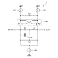
まず、第1実施形態に係る発振器の構成について、図1を参照して説明する。図1は、第1実施形態に係る発振器の構成を示す回路図である。図1に示すように、発振器1は、第1の端子である端子OUT1と、第2の端子である端子OUT2と、端子OUT1と端子OUT2との間に直列に接続された抵抗素子R2及びインダクタL2と、抵抗素子R2と並列に接続された振動子110と、端子OUT1と端子OUT2との間に接続されたコンデンサC2と、端子OUT1と端子OUT2との間に接続され、振動子110を振動させるクロスカップル型回路で構成された発振回路部100と、を含んで構成されている。
(First embodiment)
<Configuration of oscillator>
First, the configuration of the oscillator according to the first embodiment will be described with reference to FIG. FIG. 1 is a circuit diagram showing a configuration of an oscillator according to the first embodiment. As shown in FIG. 1, the
発振回路部100は、第1の能動素子であるNchトランジスタN1と、第2の能動素子であるNchトランジスタN2と、を含み、NchトランジスタN1のゲート端子がNchトランジスタN2のソース端子に接続され、NchトランジスタN2のゲート端子がNchトランジスタN1のソース端子に接続され、クロスカップル型回路を構成している。NchトランジスタN1のソース端子は、電流源121を介して電源電位VDDと接続され、NchトランジスタN2のソース端子は、電流源122を介して電源電位VDDと接続されている。さらに、NchトランジスタN1のソース端子とNchトランジスタN2のソース端子との間には、コンデンサCaが接続されている。
The
端子OUT1と端子OUT2とは、電流源120を介して接地電位GNDに接続されている。
The terminals OUT1 and OUT2 are connected to the ground potential GND through the
振動子110は、SAW振動子で構成されており、振動子110の等価回路111は、図5(B)に示すように、直列に接続された等価直列インダクタL1と等価直列コンデンサC1と等価直列抵抗R1と、これらと平行に接続された等価並列コンデンサC0とからなる回路で表現される。
The
<発振器の動作>
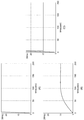
次に、発振器の動作について図2を参照して説明する。図2は、発振器の動作を示すタイミング図である。
<Oscillator operation>
Next, the operation of the oscillator will be described with reference to FIG. FIG. 2 is a timing diagram showing the operation of the oscillator.
図2(A)は、端子OUT1と端子OUT2との間に接続された抵抗素子R2とインダクタL2とコンデンサC2とで構成されるLC並列共振回路の発振時間を示すタイミング図である。抵抗素子R2は、等価回路111の等価直列抵抗R1の抵抗値よりも大きい値で設定され、インダクタL2は、等価回路111の等価直列インダクタL1よりも小さい値で設定されている。抵抗素子R2とインダクタL2とコンデンサC2とで構成されるLC並列共振回路のQ特性Q2は、角周波数をωとすると、Q2=ω×L2/R2となり、発振起動時間td2は、td2=(2×Q2)/ω=2×L2/R2となる。図2(A)に示すように、抵抗素子R2とインダクタL2とコンデンサC2とで構成されるLC並列共振回路は、約6μ秒の時点で発振周波数が24MHzに達するように構成されているものとする。
FIG. 2A is a timing chart showing an oscillation time of an LC parallel resonance circuit composed of a resistance element R2, an inductor L2, and a capacitor C2 connected between the terminal OUT1 and the terminal OUT2. The resistance element R2 is set to a value larger than the resistance value of the equivalent series resistance R1 of the
一方、図2(B)は、端子OUT1と端子OUT2との間に接続された振動子110とインダクタL2とコンデンサC2とで構成されるLC並列共振回路の発振時間を示すタイミング図である。振動子110とインダクタL2とコンデンサC2とで構成されるLC並列共振回路のQ特性Q1は、Q1=ω×(L1+L2)/R1となり、発振起動時間td1は、td1=(2×Q1)/ω=2×(L1+L2)/R1となる。インダクタL2の値はインダクタL1の値よりも格段に小さいので、発振起動時間td1は、td1≒2×L1/R1となる。図2(B)に示すように、振動子110とインダクタL2とコンデンサC2とで構成されるLC並列共振回路は、0秒から発振周波数が徐々に大きくなり、約100μ秒の時点で発振周波数が10MHzに達するように構成されているものとする。
On the other hand, FIG. 2B is a timing diagram showing an oscillation time of an LC parallel resonance circuit composed of the
ここで、発振起動時間td2が発振起動時間td1よりもかなり短くなった理由は、LC並列共振回路のQ特性Q2は、Q特性Q1よりも桁違いに小さいからである。 Here, the reason why the oscillation start time td2 is considerably shorter than the oscillation start time td1 is that the Q characteristic Q2 of the LC parallel resonant circuit is orders of magnitude smaller than the Q characteristic Q1.
発振起動時間td2は、前述のようにtd2=2×L2/R2であり、発振起動時間td1は、td1=L1/R1であるので、L2/R2<L1/R1であれば、td2<td1となる。 As described above, the oscillation start time td2 is td2 = 2 × L2 / R2, and the oscillation start time td1 is td1 = L1 / R1, so if L2 / R2 <L1 / R1, then td2 <td1 Become.
ここで、抵抗素子R2の抵抗値を等価回路111の等価直列抵抗R1の抵抗値よりも大きい値で設定しても、発振起動時間td2を発振起動時間td1よりも短くすることができる。インダクタL2を等価回路111の等価直列インダクタL1よりも小さい値で設定しても、発振起動時間td2を発振起動時間td1よりも短くすることができる。
Here, even if the resistance value of the resistance element R2 is set to a value larger than the resistance value of the equivalent series resistance R1 of the
図2(C)は、発振器1の発振時間を示すタイミング図である。発振器1は、(td2=)約6μ秒の時点で抵抗素子R2とインダクタL2とコンデンサC2とで構成されるLC並列共振回路による発振周波数=24MHzに達した直後、振動子110とインダクタL2とコンデンサC2とで構成される並列共振回路による発振周波数=10MHzになる。
FIG. 2C is a timing chart showing the oscillation time of the
以上に述べた本実施形態によれば、以下の効果が得られる。 According to the present embodiment described above, the following effects can be obtained.
本実施形態では、振動子が発振を開始するまでの期間にインダクタとコンデンサにより構成されるLC並列発振回路が先に発振をするので振動子単体より短時間で起動することができ、振動子が発振を開始すれば周波数純度の高い発振器を実現できる。 In this embodiment, since the LC parallel oscillation circuit composed of the inductor and the capacitor oscillates first in the period until the vibrator starts oscillating, the vibrator can be activated in a shorter time than the vibrator alone. If oscillation is started, an oscillator with high frequency purity can be realized.
以上、発振器の実施形態を説明したが、こうした実施の形態に何ら限定されるものではなく、趣旨を逸脱しない範囲内において様々な形態で実施し得ることができる。以下、変形例を挙げて説明する。 Although the embodiments of the oscillator have been described above, the present invention is not limited to these embodiments, and can be implemented in various forms without departing from the spirit. Hereinafter, a modification will be described.
(変形例1)発振器の変形例1について説明する。前記第1実施形態では、発振回路部100をNchトランジスタN1,N2で構成した場合を説明したが、Pchトランジスタで構成してもよい。
(Modification 1)
(変形例2)発振器の変形例2について説明する。前記第1実施形態の発振器1のコンデンサC2とインダクタL2を、図3に示すように逆に配置してもよい。
(Modification 2) Modification 2 of the oscillator will be described. The capacitor C2 and the inductor L2 of the
(変形例3)発振器の変形例3について説明する。前記第1実施形態の発振器1に含まれる抵抗素子R2を、図4に示すように可変抵抗素子VR2にしてもよい。可変抵抗素子VR2により、起動時間を制御することができる。
(Modification 3) Modification 3 of the oscillator will be described. The resistance element R2 included in the
(変形例4)発振器の変形例4について説明する。前記第1実施形態では、振動子110をSAW振動子で構成した場合を説明したが、音叉型振動子、AT振動子、FBAR(Film Bulk Acoustic Resonator)、MEMS振動子、SMR(Solid Mounted Resonator)などで構成してもよい。
(Modification 4) Modification 4 of the oscillator will be described. In the first embodiment, the case where the
1…発振器、100…発振回路部、110…振動子、111…等価回路、120,121,122…電流源。
DESCRIPTION OF
Claims (5)
第2の端子と、
前記第1の端子と前記第2の端子との間に、直列に接続された抵抗素子及びインダクタと、
前記抵抗素子と並列に接続された振動子と、
前記第1の端子と前記第2の端子との間に接続されたコンデンサと、
前記第1の端子と前記第2の端子との間に接続され、前記振動子を振動させる発振回路部と、
を含み、
前記インダクタの値と前記抵抗素子の抵抗値と前記振動子の等価直列インダクタの値と前記振動子の等価直列抵抗の抵抗値とは、
(前記インダクタの値÷前記抵抗素子の抵抗値)<(前記振動子の等価直列インダクタの値÷前記振動子の等価直列抵抗の抵抗値)の関係を満たす、
ことを特徴とする発振器。 A first terminal;
A second terminal;
A resistance element and an inductor connected in series between the first terminal and the second terminal;
A vibrator connected in parallel with the resistance element;
A capacitor connected between the first terminal and the second terminal;
An oscillation circuit unit that is connected between the first terminal and the second terminal and vibrates the vibrator;
Including
The value of the inductor, the resistance value of the resistance element, the value of the equivalent series inductor of the vibrator, and the resistance value of the equivalent series resistance of the vibrator are:
Satisfying the relationship (value of the inductor / resistance value of the resistive element) <(value of equivalent series inductor of the vibrator / resistance value of equivalent series resistance of the vibrator).
An oscillator characterized by that.
第2の端子と、
前記第1の端子と前記第2の端子との間に、直列に接続された抵抗素子及びコンデンサと、
前記抵抗素子と並列に接続された振動子と、
前記第1の端子と前記第2の端子との間に接続されたインダクタと、
前記第1の端子と前記第2の端子との間に接続され、前記振動子を振動させる発振回路部と、
を含み、
前記インダクタの値と前記抵抗素子の抵抗値と前記振動子の等価直列インダクタの値と前記振動子の等価直列抵抗の抵抗値とは、
(前記インダクタの値÷前記抵抗素子の抵抗値)<(前記振動子の等価直列インダクタの値÷前記振動子の等価直列抵抗の抵抗値)の関係を満たす、
ことを特徴とする発振器。 A first terminal;
A second terminal;
A resistance element and a capacitor connected in series between the first terminal and the second terminal;
A vibrator connected in parallel with the resistance element;
An inductor connected between the first terminal and the second terminal;
An oscillation circuit unit that is connected between the first terminal and the second terminal and vibrates the vibrator;
Including
The value of the inductor, the resistance value of the resistance element, the value of the equivalent series inductor of the vibrator, and the resistance value of the equivalent series resistance of the vibrator are:
Satisfying the relationship (value of the inductor / resistance value of the resistive element) <(value of equivalent series inductor of the vibrator / resistance value of equivalent series resistance of the vibrator).
An oscillator characterized by that.
Priority Applications (1)
| Application Number | Priority Date | Filing Date | Title |
|---|---|---|---|
| JP2007207516A JP5034763B2 (en) | 2007-08-09 | 2007-08-09 | Oscillator |
Applications Claiming Priority (1)
| Application Number | Priority Date | Filing Date | Title |
|---|---|---|---|
| JP2007207516A JP5034763B2 (en) | 2007-08-09 | 2007-08-09 | Oscillator |
Related Child Applications (1)
| Application Number | Title | Priority Date | Filing Date |
|---|---|---|---|
| JP2008253524A Division JP2009044756A (en) | 2008-09-30 | 2008-09-30 | Oscillator |
Publications (3)
| Publication Number | Publication Date |
|---|---|
| JP2009044479A JP2009044479A (en) | 2009-02-26 |
| JP2009044479A5 JP2009044479A5 (en) | 2010-09-24 |
| JP5034763B2 true JP5034763B2 (en) | 2012-09-26 |
Family
ID=40444731
Family Applications (1)
| Application Number | Title | Priority Date | Filing Date |
|---|---|---|---|
| JP2007207516A Expired - Fee Related JP5034763B2 (en) | 2007-08-09 | 2007-08-09 | Oscillator |
Country Status (1)
| Country | Link |
|---|---|
| JP (1) | JP5034763B2 (en) |
Families Citing this family (2)
| Publication number | Priority date | Publication date | Assignee | Title |
|---|---|---|---|---|
| KR101915141B1 (en) | 2016-10-18 | 2018-11-05 | 부경대학교 산학협력단 | Oscillation circuit by using two terminal elements having negative differential resistance |
| JP6870403B2 (en) * | 2017-03-16 | 2021-05-12 | セイコーエプソン株式会社 | Oscillator circuits, circuit devices, oscillators, electronic devices and mobiles |
Family Cites Families (4)
| Publication number | Priority date | Publication date | Assignee | Title |
|---|---|---|---|---|
| JP3395482B2 (en) * | 1995-10-06 | 2003-04-14 | ソニー株式会社 | Oscillation circuit and oscillation method |
| EP1265352B1 (en) * | 2001-06-07 | 2011-08-10 | CSEM Centre Suisse d'Electronique et de Microtechnique S.A. - Recherche et Développement | Differential oscillator circuit comprising an electromechanical resonator |
| JP4507070B2 (en) * | 2004-03-17 | 2010-07-21 | ソニー・エリクソン・モバイルコミュニケーションズ株式会社 | Communication device |
| JP2007096396A (en) * | 2005-09-27 | 2007-04-12 | Seiko Epson Corp | Oscillation circuit |
-
2007
- 2007-08-09 JP JP2007207516A patent/JP5034763B2/en not_active Expired - Fee Related
Also Published As
| Publication number | Publication date |
|---|---|
| JP2009044479A (en) | 2009-02-26 |
Similar Documents
| Publication | Publication Date | Title |
|---|---|---|
| JP5232231B2 (en) | Operating circuit for surface wave resonance circuit and oscillation circuit using the same | |
| US20060255882A1 (en) | Electronic apparatus | |
| JP2014096631A (en) | Self-oscillation circuit | |
| JP2008312269A (en) | Oscillation circuit, and oscillator | |
| TW201236362A (en) | Piezoelectric oscillator | |
| JP5034763B2 (en) | Oscillator | |
| JP2011188373A (en) | Piezoelectric oscillator | |
| JP2008259216A5 (en) | ||
| JP2008228334A5 (en) | ||
| JP2009044756A (en) | Oscillator | |
| JP2007103985A (en) | Crystal oscillator | |
| JP2003273703A5 (en) | ||
| JP6220618B2 (en) | Resonant circuit and oscillation circuit | |
| RU2004128125A (en) | QUARTZ RESONATOR | |
| JP6001290B2 (en) | Oscillator circuit | |
| JP6097615B2 (en) | Crystal oscillator | |
| JP2002232234A (en) | Complex crystal resonator and overtone crystal oscillator using the same | |
| JP2004104631A (en) | Crystal oscillator circuit | |
| JP6212343B2 (en) | Resonant circuit and oscillation circuit | |
| JP2015171080A (en) | voltage-controlled oscillator | |
| JP5533051B2 (en) | Oscillator with signal generator | |
| TWI691163B (en) | Start-oscillation circuit and operation method thereof | |
| JP2003273647A5 (en) | ||
| JP2003273649A5 (en) | Electronic device equipped with crystal unit and manufacturing method thereof | |
| JP2002217644A (en) | Crystal oscillator |
Legal Events
| Date | Code | Title | Description |
|---|---|---|---|
| A521 | Written amendment |
Free format text: JAPANESE INTERMEDIATE CODE: A523 Effective date: 20100805 |
|
| A621 | Written request for application examination |
Free format text: JAPANESE INTERMEDIATE CODE: A621 Effective date: 20100805 |
|
| A977 | Report on retrieval |
Free format text: JAPANESE INTERMEDIATE CODE: A971007 Effective date: 20120529 |
|
| TRDD | Decision of grant or rejection written | ||
| A01 | Written decision to grant a patent or to grant a registration (utility model) |
Free format text: JAPANESE INTERMEDIATE CODE: A01 Effective date: 20120605 |
|
| A01 | Written decision to grant a patent or to grant a registration (utility model) |
Free format text: JAPANESE INTERMEDIATE CODE: A01 |
|
| A61 | First payment of annual fees (during grant procedure) |
Free format text: JAPANESE INTERMEDIATE CODE: A61 Effective date: 20120618 |
|
| FPAY | Renewal fee payment (event date is renewal date of database) |
Free format text: PAYMENT UNTIL: 20150713 Year of fee payment: 3 |
|
| R150 | Certificate of patent or registration of utility model |
Free format text: JAPANESE INTERMEDIATE CODE: R150 |
|
| S531 | Written request for registration of change of domicile |
Free format text: JAPANESE INTERMEDIATE CODE: R313531 |
|
| R350 | Written notification of registration of transfer |
Free format text: JAPANESE INTERMEDIATE CODE: R350 |
|
| LAPS | Cancellation because of no payment of annual fees |