JP5032157B2 - Liquid crystal display - Google Patents
Liquid crystal display Download PDFInfo
- Publication number
- JP5032157B2 JP5032157B2 JP2007054729A JP2007054729A JP5032157B2 JP 5032157 B2 JP5032157 B2 JP 5032157B2 JP 2007054729 A JP2007054729 A JP 2007054729A JP 2007054729 A JP2007054729 A JP 2007054729A JP 5032157 B2 JP5032157 B2 JP 5032157B2
- Authority
- JP
- Japan
- Prior art keywords
- liquid crystal
- region
- area
- color filter
- electrode
- Prior art date
- Legal status (The legal status is an assumption and is not a legal conclusion. Google has not performed a legal analysis and makes no representation as to the accuracy of the status listed.)
- Expired - Fee Related
Links
Images


Classifications
-
- G—PHYSICS
- G02—OPTICS
- G02F—OPTICAL DEVICES OR ARRANGEMENTS FOR THE CONTROL OF LIGHT BY MODIFICATION OF THE OPTICAL PROPERTIES OF THE MEDIA OF THE ELEMENTS INVOLVED THEREIN; NON-LINEAR OPTICS; FREQUENCY-CHANGING OF LIGHT; OPTICAL LOGIC ELEMENTS; OPTICAL ANALOGUE/DIGITAL CONVERTERS
- G02F1/00—Devices or arrangements for the control of the intensity, colour, phase, polarisation or direction of light arriving from an independent light source, e.g. switching, gating or modulating; Non-linear optics
- G02F1/01—Devices or arrangements for the control of the intensity, colour, phase, polarisation or direction of light arriving from an independent light source, e.g. switching, gating or modulating; Non-linear optics for the control of the intensity, phase, polarisation or colour
- G02F1/13—Devices or arrangements for the control of the intensity, colour, phase, polarisation or direction of light arriving from an independent light source, e.g. switching, gating or modulating; Non-linear optics for the control of the intensity, phase, polarisation or colour based on liquid crystals, e.g. single liquid crystal display cells
- G02F1/133—Constructional arrangements; Operation of liquid crystal cells; Circuit arrangements
- G02F1/1333—Constructional arrangements; Manufacturing methods
- G02F1/1335—Structural association of cells with optical devices, e.g. polarisers or reflectors
- G02F1/133553—Reflecting elements
- G02F1/133555—Transflectors
-
- G—PHYSICS
- G02—OPTICS
- G02F—OPTICAL DEVICES OR ARRANGEMENTS FOR THE CONTROL OF LIGHT BY MODIFICATION OF THE OPTICAL PROPERTIES OF THE MEDIA OF THE ELEMENTS INVOLVED THEREIN; NON-LINEAR OPTICS; FREQUENCY-CHANGING OF LIGHT; OPTICAL LOGIC ELEMENTS; OPTICAL ANALOGUE/DIGITAL CONVERTERS
- G02F1/00—Devices or arrangements for the control of the intensity, colour, phase, polarisation or direction of light arriving from an independent light source, e.g. switching, gating or modulating; Non-linear optics
- G02F1/01—Devices or arrangements for the control of the intensity, colour, phase, polarisation or direction of light arriving from an independent light source, e.g. switching, gating or modulating; Non-linear optics for the control of the intensity, phase, polarisation or colour
- G02F1/13—Devices or arrangements for the control of the intensity, colour, phase, polarisation or direction of light arriving from an independent light source, e.g. switching, gating or modulating; Non-linear optics for the control of the intensity, phase, polarisation or colour based on liquid crystals, e.g. single liquid crystal display cells
- G02F1/133—Constructional arrangements; Operation of liquid crystal cells; Circuit arrangements
- G02F1/1333—Constructional arrangements; Manufacturing methods
- G02F1/1335—Structural association of cells with optical devices, e.g. polarisers or reflectors
-
- G—PHYSICS
- G02—OPTICS
- G02F—OPTICAL DEVICES OR ARRANGEMENTS FOR THE CONTROL OF LIGHT BY MODIFICATION OF THE OPTICAL PROPERTIES OF THE MEDIA OF THE ELEMENTS INVOLVED THEREIN; NON-LINEAR OPTICS; FREQUENCY-CHANGING OF LIGHT; OPTICAL LOGIC ELEMENTS; OPTICAL ANALOGUE/DIGITAL CONVERTERS
- G02F1/00—Devices or arrangements for the control of the intensity, colour, phase, polarisation or direction of light arriving from an independent light source, e.g. switching, gating or modulating; Non-linear optics
- G02F1/01—Devices or arrangements for the control of the intensity, colour, phase, polarisation or direction of light arriving from an independent light source, e.g. switching, gating or modulating; Non-linear optics for the control of the intensity, phase, polarisation or colour
- G02F1/13—Devices or arrangements for the control of the intensity, colour, phase, polarisation or direction of light arriving from an independent light source, e.g. switching, gating or modulating; Non-linear optics for the control of the intensity, phase, polarisation or colour based on liquid crystals, e.g. single liquid crystal display cells
- G02F1/133—Constructional arrangements; Operation of liquid crystal cells; Circuit arrangements
- G02F1/1333—Constructional arrangements; Manufacturing methods
- G02F1/1337—Surface-induced orientation of the liquid crystal molecules, e.g. by alignment layers
- G02F1/133707—Structures for producing distorted electric fields, e.g. bumps, protrusions, recesses, slits in pixel electrodes
Description
本発明は、液晶表示装置に関し、特に負の誘電率異方性を有する液晶を使用したMVA方式の液晶表示装置に関する。 The present invention relates to a liquid crystal display device, and more particularly to an MVA liquid crystal display device using a liquid crystal having negative dielectric anisotropy.
近年、携帯電話、携帯音楽プレーヤーなどといった携帯情報端末の分野では、画像や文字の表示装置として反射表示領域と透過表示領域を併せ持つ半透過型の液晶表示装置が多く用いられている。この液晶表示装置では、反射表示領域においては外光からの反射光を、透過表示領域においてはバックライト光による透過光を画像表示の光源として用いるので、室内や屋外などの照明環境に依存することなく視認性が良い。 In recent years, in the field of portable information terminals such as mobile phones and portable music players, transflective liquid crystal display devices having both a reflective display region and a transmissive display region are often used as image and character display devices. In this liquid crystal display device, reflected light from outside light is used as the light source for image display in the reflective display area, and transmitted light from the backlight is used as the light source for image display in the transmissive display area. There is no visibility.
半透過型の液晶表示装置には、透過表示領域における液晶層の厚み(以下、「セルギャップ」と称する)と反射表示領域におけるセルギャップが同一であるシングルギャップ方式のものと透過表示領域のセルギャップの方が反射表示領域のセルギャップよりも厚い、いわゆるマルチギャップ方式のものとがある。 The transflective liquid crystal display device includes a single gap type cell in which the thickness of the liquid crystal layer in the transmissive display region (hereinafter referred to as “cell gap”) and the cell gap in the reflective display region are the same, and a cell in the transmissive display region. There is a so-called multi-gap type in which the gap is thicker than the cell gap in the reflective display region.
一般的に使用されるマルチギャップ方式の液晶表示装置では、透過表示領域において光は液晶層を一度通過する。これに対し、反射表示領域において光はカラーフィルタ層を二度通過するため、表示色が濃く、暗くなってしまい、ホワイトバランスがずれてしまうなどの問題がある。最近では反射表示領域のカラーフィルタ層に透明領域を設けることで明るさを確保すると共に、透明領域の面積をカラーフィルタ層の色毎に調整して、透過表示領域と反射表示領域とで色の濃さを同程度にする技術が提案されている。 In a commonly used multi-gap liquid crystal display device, light passes through the liquid crystal layer once in the transmissive display region. On the other hand, since light passes through the color filter layer twice in the reflective display area, the display color becomes dark and dark, and the white balance shifts. Recently, by providing a transparent area in the color filter layer of the reflective display area, brightness is secured, and the area of the transparent area is adjusted for each color of the color filter layer, so that the color of the transparent display area and the reflective display area can be changed. A technique for making the darkness comparable is proposed.
一方で、液晶表示装置において、負の誘電率異方性を有する液晶を使用して、液晶分子を基板に対して垂直に配向させ、液晶の複屈折率を略ゼロにすることにより、十分な黒表示を実現すると共に、より高いコントラストを得ることが可能なVertical Alignment方式(以下、VA方式と称する)の液晶表示装置が提案されている。また、基板上に配置した誘電体の突起物により、液晶分子の傾斜方向を複数の領域に分割するMulti Vertical Alignment方式(以下、MVA方式と称する)の液晶表示装置は、コントラスト等の表示品位が良好であると共に広い視野角特性を有する。 On the other hand, in a liquid crystal display device, by using a liquid crystal having negative dielectric anisotropy, the liquid crystal molecules are aligned perpendicularly to the substrate, and the birefringence of the liquid crystal is made substantially zero. A liquid crystal display device of a vertical alignment method (hereinafter referred to as a VA method) capable of realizing black display and obtaining higher contrast has been proposed. In addition, the liquid crystal display device of the Multi Vertical Alignment method (hereinafter referred to as the MVA method) that divides the tilt direction of the liquid crystal molecules into a plurality of regions by a dielectric protrusion disposed on the substrate has a display quality such as contrast. It is good and has a wide viewing angle characteristic.
透過表示領域と反射表示領域を備えたMVA方式の液晶表示装置において配置された突起物は誘電体であるため、液晶層を通過する光が突起物により吸収され、反射表示領域における反射率が低下してしまう。これに対し、最近では突起物を、カラーフィルタ層に設けた透明領域と平面的に重なるように配置することで明るさを確保すると共に、カラーフィルタ層の色毎に選択的に実施することでホワイトバランスを調整する技術が開示されている(例えば、特許文献1参照)。
しかしながら、上記液晶表示装置において突起物と透明領域とが重なった領域では、突起物の厚さが厚いために、透明領域による反射率低下の抑制効果が十分でなく、所望の特性を得ることができない。 However, in the area where the protrusions and the transparent region overlap in the liquid crystal display device, since the protrusions are thick, the effect of suppressing the decrease in reflectance by the transparent region is not sufficient, and desired characteristics can be obtained. Can not.
また、突起物あるいは電極に設けられたスリットと透明領域とを平面的に重ねただけの構成では、製造時において合わせズレが生じた場合に、カラーフィルタ層の着色領域と透明領域との面積の比率がずれてしまう。このため、カラーフィルタ層の色度がばらつき、ホワイトバランスが予め設定した値からずれやすくなるといった問題がある。 In addition, in the configuration in which the slit provided on the protrusion or the electrode and the transparent region are simply overlapped in a planar manner, when the misalignment occurs at the time of manufacture, the area of the color region of the color filter layer and the transparent region is reduced. The ratio will shift. For this reason, there is a problem in that the chromaticity of the color filter layer varies and the white balance tends to deviate from a preset value.
本発明は、上記に鑑みてなされたものであり、反射表示領域を有するMVA方式の液晶表示装置において、誘電体の突起物等の構造物に起因した反射表示における反射率低下の抑制、及び、製造時における誘電体の突起物、あるいは、スリット等の構造物とカラーフィルタ層の着色領域と透明領域との合わせズレから生じるホワイトバランスのずれを抑制することを課題とする。 The present invention has been made in view of the above, and in a MVA liquid crystal display device having a reflective display region, it is possible to suppress a decrease in reflectance in reflective display caused by a structure such as a dielectric protrusion, and It is an object of the present invention to suppress a white balance shift caused by a misalignment between a dielectric protrusion or a structure such as a slit and a colored region and a transparent region of a color filter layer during manufacturing.
本発明に係る液晶表示装置は、対向して配置されたアレイ基板及び対向基板と、前記アレイ基板及び対向基板の間隙に挟持され、負の誘電率異方性を有する液晶分子からなる液晶層と、前記アレイ基板上の対向基板側に配置された反射電極及び透過電極と、前記対向基板上のアレイ基板側に前記反射電極及び透過電極に対応した領域に設けられたカラーフィルタ層と、前記カラーフィルタ層の前記反射電極に対応した領域内部に設けられた着色されない透明領域と、前記カラーフィルタ層上において前記反射電極及び透過電極に対向して配置された対向電極と、前記透明領域に平面的に重なり、且つ、前記反射電極あるいは前記対向電極の少なくともいずれか一方に前記液晶分子の傾斜方向を制御するために設けられた構造物と、を備え、前記透明領域及び前記構造物は、製造ばらつきにより相対的に位置がずれた場合でも、透明領域が前記構造物に重なる領域の面積と重ならない領域の面積との比率が一定となるような形状であることを特徴とする。 A liquid crystal display device according to the present invention includes an array substrate and a counter substrate arranged to face each other, a liquid crystal layer made of liquid crystal molecules sandwiched between the array substrate and the counter substrate, and having negative dielectric anisotropy. A reflective electrode and a transmissive electrode disposed on the counter substrate side on the array substrate; a color filter layer provided on a region corresponding to the reflective electrode and the transmissive electrode on the array substrate side on the counter substrate; and the color A transparent region that is not colored and is provided inside the region corresponding to the reflective electrode of the filter layer, a counter electrode that is disposed on the color filter layer so as to face the reflective electrode and the transmissive electrode, and is planar to the transparent region. And a structure provided to control the tilt direction of the liquid crystal molecules on at least one of the reflective electrode and the counter electrode, The transparent area and the structure have a shape in which the ratio of the area of the area where the transparent area overlaps the structure to the area of the area where the transparent area does not overlap is constant even when the position is relatively shifted due to manufacturing variations. It is characterized by that.
本発明にあっては、カラーフィルタ層の反射電極に対応した領域内部に設けられた着色されない透明領域と透明領域に平面的に重なるように設けられた構造物が、製造ばらつきにより相対的に位置がずれた場合でも、重なった領域の面積と重ならない領域の面積との比率を一定となるような形状としたことで、構造物により損失した光量を突起物に重ならない透明領域により確実に確保することができると共に、カラーフィルタ層の着色された領域とそれ以外の領域との面積比率が一定となるので色度のばらつきを抑制することができる。 In the present invention, the non-colored transparent region provided inside the region corresponding to the reflective electrode of the color filter layer and the structure provided so as to overlap the transparent region in a plane are relatively positioned due to manufacturing variations. Even in the case of misalignment, the ratio of the area of the overlapped area to the area of the non-overlapping area is made constant so that the amount of light lost by the structure is reliably secured by the transparent area that does not overlap the protrusion. In addition, since the area ratio between the colored region of the color filter layer and the other region is constant, variation in chromaticity can be suppressed.
上記液晶表示装置における透明領域及び構造物は、互いに交差配置可能な形状、若しくは、構造物が透明領域の範囲内に配置可能な形状であることが望ましい。 It is desirable that the transparent region and the structure in the liquid crystal display device have shapes that can be arranged to cross each other or shapes that can be arranged within the range of the transparent region.
本発明の液晶表示装置によれば、液晶分子の配向を制御する構造物に起因した反射表示における反射率低下およびホワイトバランスのずれを抑制することができる。 According to the liquid crystal display device of the present invention, it is possible to suppress a decrease in reflectance and a deviation in white balance in reflective display caused by a structure that controls the alignment of liquid crystal molecules.
以下、本発明の実施の形態について図面を用いて説明する。 Hereinafter, embodiments of the present invention will be described with reference to the drawings.
[第1の実施の形態]
図1は、第1の実施の形態に係る液晶表示装置(以下、本液晶表示装置と称する)の一画素の構成を概略的に示す断面図である。同図に示すように、本液晶表示装置は、アレイ基板100と、アレイ基板100と対向して配置された対向基板200と、アレイ基板100と対向基板200の間隙に挟持された負の誘電率異方性を有する液晶分子301からなる液晶層300を備える。ここでアレイ基板100の背面側には図示しないバックライトが配置される。
[First Embodiment]
FIG. 1 is a cross-sectional view schematically showing a configuration of one pixel of the liquid crystal display device (hereinafter referred to as the present liquid crystal display device) according to the first embodiment. As shown in the figure, the present liquid crystal display device includes an
アレイ基板100は、ガラス基板101上に形成された透明樹脂層102上において、画素電極として凸凹状の反射電極103が形成された反射表示領域と透過電極104が形成された透過表示領域とを画素毎に備える。ここで透過電極104は一部除去されてスリット105が設けられる。スリット105は、例えば長さ10マイクロメートル、幅4マイクロメートルのサイズとする。反射電極103と透過電極104の上には垂直配向膜107が形成される。透明樹脂層102には画素電極駆動用の薄膜トランジスタ、薄膜トランジスタに接続される信号線や走査線などの信号配線が形成される。ガラス基板101の外側には偏光板108が配置される。
The
対向基板200は、ガラス基板201上のアレイ基板100側に反射電極103及び透過電極104に対応した領域にカラーフィルタ層202が設けられ、カラーフィルタ層202の反射電極103に対応した領域内部には着色されない透明領域203が設けられる。対向基板200と液晶層300との間の反射電極103に対応する反射表示領域においては、液晶層300の厚さを調整するための液晶層厚調整層としての段差204が設けられる。段差の材質には例えば誘電体を使用する。このような段差204を設けることで、反射表示領域におけるセルギャップを透過表示領域におけるセルギャップよりも薄くしてマルチギャップ方式の液晶表示装置としている。
The
カラーフィルタ層202及び段差204上においては、反射電極103及び透過電極104に対向して対向電極205が配置される。対向電極205には、光透過性の高い導電性材料としてITOを使用する。対向電極205上には、液晶分子301の傾斜方向を制御するための構造物である誘電体の突起物206a、206bが設けられる。これにより、液晶分子301の傾斜方向を複数の領域に分割するMVA方式の液晶表示装置としている。ここで突起物206a、206bは、例えば高さ1マイクロメートル、幅6マイクロメートルのサイズでアレイ基板100側突出し、一方向に伸びて設けられ画素の中央付近で分断される。対向電極205と突起物206a、206bの上には垂直配向膜207が形成される。
On the
このように突起物206a、206bを断続的に設けることで、分断部分では液晶層300を通過する光量が増加すると共に、突起物206a、206bの分断部分に対向して設けられたスリット105により、分断部分に位置する液晶分子301の傾斜方向を制御することができる。
By providing the
尚、上記突起物206a、206bの代わりに対向電極205の一部分を除去したスリットにしても良い。このスリットは、上記突起物206a、206bと同様に液晶分子301の傾斜方向を制御する構造物となる。
Note that a slit obtained by removing a part of the
液晶層300中の負の誘電率異方性を有する液晶分子301は、透過電極104及び反射電極103と対向電極205との間に電圧を印加していない状態、あるいは、しきい値未満の電圧を印加した状態で垂直配向膜107,207により基板に対して垂直に配向され、透過電極104及び反射電極103と対向電極205との間にしきい値以上の電圧を印加した状態では基板に対し傾斜あるいは概略平行に配列し、この傾斜する方位は電気力線の向きに概略規定される性質を持つ。
The
液晶層300中のアレイ基板100と対向基板200の間隙にはスペーサ302が配置される。ここでは、例えば、高さ2.0マイクロメートルの柱状スペーサが配置される。
A
このような構成により、本液晶表示装置は、反射電極103で反射される反射光およびバックライトにより照射され透過電極104を透過する光を光源として用いると共に、液晶層300への印加電圧を変化させる。このとき液晶層300中に発生した電界により、垂直に配向していた液晶分子301が傾斜することにより、階調が連続的に変化可能となるので、反射モードおよび透過モードによりカラー画像が表示可能となる。
With this configuration, the liquid crystal display device uses the reflected light reflected by the
図2は、図1の一画素を上から見た平面図である。同図に示すように、一画素は、赤色・緑色・青色のカラーフィルタ層202R・202G・202Bに対応して配置された3つの副画素から構成される。反射表示領域において赤、緑、青の3色のうち赤、緑の2色のカラーフィルタ層202R、202Gに透明領域203が設けられる。透明領域203は突起物206aと平面的に重なるように設けられる。これにより、突起物206aが配置された領域で吸収される光が、透明領域203では通過しやすくなるので明るさが確保され、反射率の低下が抑制される。
FIG. 2 is a plan view of one pixel of FIG. 1 as viewed from above. As shown in the drawing, one pixel is composed of three sub-pixels arranged corresponding to the red, green, and blue color filter layers 202R, 202G, and 202B. In the reflective display area, a
更に、反射表示領域においてカラーフィルタ層の着色領域の面積に対する透明領域の面積比率は緑画素>赤画素>青画素となるように調整する。このようにして、カラーフィルタ層のそれぞれの色度を調整し、一画素が表示するホワイトバランスを予め一定の値に調整している。 Furthermore, the area ratio of the transparent area to the area of the colored area of the color filter layer in the reflective display area is adjusted so that green pixel> red pixel> blue pixel. In this way, each chromaticity of the color filter layer is adjusted, and the white balance displayed by one pixel is adjusted to a predetermined value in advance.
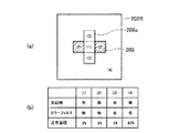
次に、透明領域と突起物の形状について図3を用いて説明する。同図(a)の平面図は、図2の反射表示領域におけるカラーフィルタ層202Rと透明領域203と突起物206aのみを示している。ここで領域(1)とは透明領域が突起物と重なった領域を、領域(2)とは透明領域が突起物と重ならない領域を、領域(3)とはカラーフィルタ層に対応して突起物のみが配置されている領域を、領域(4)とは上記領域(1)〜(3)以外のカラーフィルタ層の着色領域を指す。
Next, the shape of the transparent region and the protrusion will be described with reference to FIG. The plan view of FIG. 6A shows only the
同図(b)のチャートは、カラーフィルタ層202Rの総面積に対する領域(1)〜領域(4)のそれぞれが占める面積を示している。ここでは総面積を100%として、領域(1)〜領域(4)の面積は単位を%で示している。同図に示すように、各領域の占有面積について、例えば領域(1)が3%、領域(2)が6%、領域(3)が6%、領域(4)が85%となるように赤色の色度を設定する。ここでは図示しないが、緑色のカラーフィルタ層においても同様に、各領域(1)〜(4)の面積を調整して緑色の色度を設定する。このようにして赤・緑・青色による一画素のホワイトバランスの値が設定される。
The chart of FIG. 5B shows the area occupied by each of the regions (1) to (4) with respect to the total area of the
突起物206a及び透明領域203は、互いに交差配置可能な長方形であって、互いに交差して配置されている。このような構成とすることで、透明領域203と、突起物206aとが製造ばらつきにより相対的に位置がずれた場合でも、透明領域が突起物と重なった領域(1)の面積と重ならない領域(2)の面積との比率が一定となる。これにより、領域(1)で突起物により吸収され損失した光量を、領域(2)で突起物に重ならない透明領域により確実に確保することができ、反射表示における反射率低下を抑制することができる。
The
また、カラーフィルタ層の着色領域(4)とそれ以外の領域(1)〜(3)との面積比率が一定となるので色度のばらつきを抑制し、ホワイトバランスのずれを抑制することができる。 In addition, since the area ratio between the colored region (4) of the color filter layer and the other regions (1) to (3) is constant, variation in chromaticity can be suppressed and deviation in white balance can be suppressed. .
したがって、第1の実施の形態によれば、反射表示領域に対応してカラーフィルタ層202R、202Gに設けられた透明領域203と透明領域に平面的に重なるように設けられた誘電体の突起物206aが、製造ばらつきにより相対的に位置がずれた場合でも、透明領域が突起物と重なった領域(1)の面積と重ならない領域(2)の面積との比率が一定となるので、領域(1)で突起物により損失した光量を、領域(2)で突起物に重ならない透明領域により確実に確保することができると共に、カラーフィルタ層の着色領域(4)とそれ以外の領域(1)〜(3)との面積比率が一定となるので色度のばらつきを抑制することができる。
Therefore, according to the first embodiment, the
よって、誘電体の突起物に起因した反射表示における反射率低下およびホワイトバランスのずれを抑制することができる。 Therefore, it is possible to suppress a decrease in reflectance and a deviation in white balance in the reflective display due to the dielectric protrusion.
尚、第1の実施の形態においては、突起物及び透明領域の形状は長方形であって、互いに交差して配置したが、これに限られるものではなく、互いに交差配置可能な形状であれば、透明領域及び突起物は、例えば、楕円形でもよい。 In the first embodiment, the shape of the protrusion and the transparent region is a rectangle and is arranged so as to intersect with each other. However, the shape is not limited to this. The transparent region and the protrusion may be elliptical, for example.
[第2の実施の形態]
以下、第2の実施の形態について説明する。本実施の形態に係る液晶表示装置の構成は、第1の実施の形態で説明したものと基本的な構成は同様である。以下では、第1の実施の形態と異なる点を中心に説明する。
[Second Embodiment]
Hereinafter, a second embodiment will be described. The configuration of the liquid crystal display device according to this embodiment is the same as the basic configuration described in the first embodiment. Below, it demonstrates centering on a different point from 1st Embodiment.
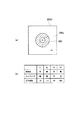
第1の実施の形態と異なる点は、図4(a)の平面図に示すように、反射表示領域のカラーフィルタ層202Rの透明領域203および突起物206aの形状として、透明領域203及び突起物206aは、突起物206aが透明領域203の範囲内に配置可能な円形である点である。
The difference from the first embodiment is that, as shown in the plan view of FIG. 4A, the
第1の実施の形態と同様に、同図(b)のチャートは、カラーフィルタ層202Rの総面積に対する領域(1)〜領域(4)のそれぞれが占める面積を示している。同図に示すように、各領域の占有面積について、例えば領域(1)が3%、領域(2)が17%、領域(3)が0%、領域(4)が80%となるように赤色の色度を設定する。ここでも図示しないが、緑色のカラーフィルタ層においても同様に、各領域(1)〜(4)の面積を調整して緑色の色度を設定し、赤・緑・青色による一画素のホワイトバランスが調整される。
Similar to the first embodiment, the chart of FIG. 4B shows the area occupied by each of the regions (1) to (4) with respect to the total area of the
このような構成においても、透明領域203と、突起物206aとが製造ばらつきにより相対的に位置がずれた場合でも、透明領域が突起物と重なった領域(1)の面積と重ならない領域(2)の面積との比率が一定となり、カラーフィルタ層の着色領域(4)とそれ以外の領域(1)〜(3)との面積比率も一定となる。
Even in such a configuration, even if the
したがって、第2の実施の形態によれば、透明領域203及び突起物206aを、突起物206aが透明領域203の範囲内に配置可能な円形としたことで、透明領域203と、誘電体の突起物206aが製造ばらつきにより相対的に位置がずれた場合でも透明領域203が突起物206aに重なる領域(2)の面積と重ならない領域(4)の面積との比率が一定となると共に、カラーフィルタ層の着色領域(4)とそれ以外の領域(1)〜(3)との面積比率も一定となるので、第1の実施の形態と同様な効果を奏することができる。
Therefore, according to the second embodiment, the
尚、第2の実施の形態においては、突起物及び透明領域の形状を円形とし、突起物を透明領域の範囲内に配置したが、これに限られるものではなく、突起物が透明領域の範囲内に配置可能な形状であれば、透明領域及び突起物は、例えば、四角形又は三角形でもよい。 In the second embodiment, the shape of the protrusion and the transparent region is circular, and the protrusion is disposed within the range of the transparent region. However, the present invention is not limited to this, and the protrusion is within the range of the transparent region. The transparent region and the protrusion may be, for example, a quadrangle or a triangle as long as the shape can be arranged inside.
また、上記の各実施の形態においては、反射表示領域において赤、緑、青の3色のうち赤、緑の2色のカラーフィルタ層に透明領域203を設け、カラーフィルタ層の着色領域の面積に対する透明領域の面積比率が緑画素>赤画素>青画素となるように調整したが、透明領域を、三色のうち少なくとも一色のカラーフィルタ層に設けるような構成であれば、これに限られるものではなく、各副画素に対応したカラーフィルタ層に透明領域を選択的に設け、着色領域に対する透明領域の面積比率を調整することで、反射表示における反射率とホワイトバランスの値を調整することができる。
Further, in each of the above embodiments, the
また、上記の各実施の形態においては、液晶層の厚さを調整するための液晶層厚調整層としての段差を対向基板と液晶層との間の反射電極に対応して設けて、マルチギャップ方式の液晶表示装置としたが、反射表示領域のセルギャップの方が透過表示領域のものよりも薄い構成であればこれに限られるものではなく、例えばアレイ基板と液晶層との間の反射電極に対応して設けてもよい。 In each of the above embodiments, a step as a liquid crystal layer thickness adjusting layer for adjusting the thickness of the liquid crystal layer is provided corresponding to the reflective electrode between the counter substrate and the liquid crystal layer, and a multi-gap is provided. However, the present invention is not limited to this as long as the cell gap of the reflective display region is thinner than that of the transmissive display region. For example, the reflective electrode between the array substrate and the liquid crystal layer You may provide corresponding to.
尚、上記の各実施の形態においては、断続的に設けられた突起物の分断部分に対向して透過電極を一部除去してスリットとし、液晶分子の傾斜方向を制御するようにしたが、これに限られるものではなく、反射電極を一部除去してスリットとし、液晶分子の傾斜方向を制御するようにしてもよい。 In each of the above embodiments, the transmission electrode is partially removed so as to face the discontinuous portions of the protrusions provided intermittently, and the tilt direction of the liquid crystal molecules is controlled. However, the present invention is not limited to this, and a part of the reflective electrode may be removed to form a slit to control the tilt direction of the liquid crystal molecules.
また、上記の各実施の形態においては、断続的に設けられた突起物の分断部分に対向した位置に透過電極又は反射電極を一部除去してスリットとし、液晶分子の傾斜方向を制御するようにしたが、これに限られるものではなく、透過電極又は反射電極上に誘電体の突起物を設けて、液晶分子の傾斜方向を制御するようにしてもよい。 Further, in each of the above embodiments, a part of the transmission electrode or the reflection electrode is removed at a position facing the discontinuous portion of the projection provided intermittently so as to form a slit so as to control the tilt direction of the liquid crystal molecules. However, the present invention is not limited to this, and a dielectric protrusion may be provided on the transmission electrode or the reflection electrode to control the tilt direction of the liquid crystal molecules.
更に、上記の各実施の形態においては、透過電極又は反射電極にスリットを設けたが、これに限られるものではなく。スリットや突起物を反射電極及び透過電極の境界をまたいで設けるような構成としてもよい。 Further, in each of the above embodiments, the slit is provided in the transmissive electrode or the reflective electrode, but the present invention is not limited to this. A configuration may be adopted in which slits or protrusions are provided across the boundary between the reflective electrode and the transmissive electrode.
また、上記の各実施の形態における液晶表示装置は、一画素に反射表示領域と透過表示領域を備えた半透過型の液晶表示装置としたが、透過表示領域のみを有する画素が配置された第1の表示領域と反射表示領域のみを有する画素が配置された第2の表示領域とを備えた液晶表示装置においても、上記各実施の形態と同様な効果を奏することができる。 In addition, the liquid crystal display device in each of the above embodiments is a transflective liquid crystal display device in which one pixel includes a reflective display region and a transmissive display region. However, a pixel having only a transmissive display region is disposed. Also in the liquid crystal display device including the second display area in which the pixels having only one display area and the reflective display area are arranged, the same effects as those of the above embodiments can be obtained.
100…アレイ基板
101…ガラス基板
102…透明樹脂層
103…反射電極
104…透過電極
105…スリット(透過電極)
107…垂直配向膜
108…偏光板
200…対向基板
201…ガラス基板
202…カラーフィルタ層
202R…カラーフィルタ層(赤色の副画素)
202G…カラーフィルタ層(緑色の副画素)
202B…カラーフィルタ層(青色の副画素)
203…透明領域(カラーフィルタ層)
204…段差
205…対向電極
206a…突起物(反射表示領域)
206b…突起物(透過表示領域)
207…垂直配向膜
300…液晶層
301…液晶分子
302…スペーサ
領域(1)…突起物と透明領域が重なった領域
領域(2)…突起物と透明領域が重ならない透明領域
領域(3)…突起物のみの領域
領域(4)…領域(1)〜(3)以外のカラーフィルタ層の着色領域
DESCRIPTION OF
DESCRIPTION OF
202G ... Color filter layer (green sub-pixel)
202B ... Color filter layer (blue subpixel)
203 ... Transparent area (color filter layer)
204 ... Step 205 ...
206b ... Projection (transparent display area)
207 ...
Claims (4)
前記アレイ基板及び対向基板の間隙に挟持され、負の誘電率異方性を有する液晶分子からなる液晶層と、
前記アレイ基板上の対向基板側に配置された反射電極及び透過電極と、
前記対向基板上のアレイ基板側に前記反射電極及び透過電極に対応した領域に設けられたカラーフィルタ層と、
前記カラーフィルタ層の前記反射電極に対応した領域内部に設けられた着色されない透明領域と、
前記カラーフィルタ層上において前記反射電極及び透過電極に対向して配置された対向電極と、
前記透明領域に平面的に重なり、且つ、前記反射電極あるいは前記対向電極の少なくともいずれか一方に前記液晶分子の傾斜方向を制御するために設けられた構造物と、を備え、
前記透明領域及び前記構造物は、製造ばらつきにより相対的に位置がずれた場合でも、透明領域が前記構造物に重なる領域の面積と重ならない領域の面積との比率が一定となるような形状であり、
前記透明領域及び前記構造物は、互いに交差配置されていることを特徴とする液晶表示装置。 An array substrate and a counter substrate arranged opposite to each other;
A liquid crystal layer made of liquid crystal molecules sandwiched between the array substrate and the counter substrate and having negative dielectric anisotropy;
A reflective electrode and a transmissive electrode disposed on the counter substrate side on the array substrate;
A color filter layer provided in a region corresponding to the reflective electrode and the transmissive electrode on the array substrate side on the counter substrate;
A non-colored transparent region provided inside the region corresponding to the reflective electrode of the color filter layer;
A counter electrode disposed on the color filter layer to face the reflective electrode and the transmissive electrode;
A structure that is planarly overlapped with the transparent region, and is provided on at least one of the reflective electrode and the counter electrode to control the tilt direction of the liquid crystal molecules,
The transparent region and the structure have a shape in which the ratio of the area of the region where the transparent region overlaps the structure and the area of the region where the transparent region does not overlap is constant even when the positions are relatively displaced due to manufacturing variations. Oh it is,
The transparent area and the structure, a liquid crystal display device which is characterized that you have been crossed each other.
前記透明領域は、前記三色のうち少なくとも一色のカラーフィルタ層に設けられることを特徴とする請求項1乃至3のいずれかに記載の液晶表示装置。 The color filter layer is composed of three color filter layers of red, green and blue,
The transparent region, the liquid crystal display device according to any one of claims 1 to 3, characterized in that provided on at least one color of the color filter layer of the three colors.
Priority Applications (5)
| Application Number | Priority Date | Filing Date | Title |
|---|---|---|---|
| JP2007054729A JP5032157B2 (en) | 2007-03-05 | 2007-03-05 | Liquid crystal display |
| US11/956,948 US7742135B2 (en) | 2007-03-05 | 2007-12-14 | Liquid crystal display device capable of preventing reflectance and white balance value from shifting |
| TW097100895A TWI382236B (en) | 2007-03-05 | 2008-01-09 | Liquid crystal display device capable of preventing reflectance and white balance value from shifting |
| CNA2008100831777A CN101261406A (en) | 2007-03-05 | 2008-03-04 | Liquid crystal display device capable of preventing reflectance and white balance value from shifting |
| KR1020080020008A KR20080081831A (en) | 2007-03-05 | 2008-03-04 | Liquid crystal display device capable of preventing reflectance and white balance value from shifting |
Applications Claiming Priority (1)
| Application Number | Priority Date | Filing Date | Title |
|---|---|---|---|
| JP2007054729A JP5032157B2 (en) | 2007-03-05 | 2007-03-05 | Liquid crystal display |
Publications (3)
| Publication Number | Publication Date |
|---|---|
| JP2008216690A JP2008216690A (en) | 2008-09-18 |
| JP2008216690A5 JP2008216690A5 (en) | 2010-04-22 |
| JP5032157B2 true JP5032157B2 (en) | 2012-09-26 |
Family
ID=39741259
Family Applications (1)
| Application Number | Title | Priority Date | Filing Date |
|---|---|---|---|
| JP2007054729A Expired - Fee Related JP5032157B2 (en) | 2007-03-05 | 2007-03-05 | Liquid crystal display |
Country Status (5)
| Country | Link |
|---|---|
| US (1) | US7742135B2 (en) |
| JP (1) | JP5032157B2 (en) |
| KR (1) | KR20080081831A (en) |
| CN (1) | CN101261406A (en) |
| TW (1) | TWI382236B (en) |
Families Citing this family (8)
| Publication number | Priority date | Publication date | Assignee | Title |
|---|---|---|---|---|
| JP5311310B2 (en) * | 2009-07-17 | 2013-10-09 | 株式会社ジャパンディスプレイ | Liquid crystal display |
| JP5566804B2 (en) | 2010-07-22 | 2014-08-06 | 株式会社ジャパンディスプレイ | LCD panel |
| JP5504215B2 (en) | 2011-07-08 | 2014-05-28 | 株式会社ジャパンディスプレイ | Liquid crystal display |
| JP5386555B2 (en) | 2011-07-28 | 2014-01-15 | 株式会社ジャパンディスプレイ | Liquid crystal display |
| JP5564473B2 (en) | 2011-08-05 | 2014-07-30 | 株式会社ジャパンディスプレイ | Liquid crystal display |
| JP5520896B2 (en) | 2011-08-08 | 2014-06-11 | 株式会社ジャパンディスプレイ | Liquid crystal display |
| CN102809858B (en) * | 2012-07-31 | 2016-03-02 | 京东方科技集团股份有限公司 | Array base palte and liquid crystal indicator |
| CN110967864B (en) * | 2019-12-23 | 2022-07-12 | Tcl华星光电技术有限公司 | Color film substrate and liquid crystal display panel |
Family Cites Families (11)
| Publication number | Priority date | Publication date | Assignee | Title |
|---|---|---|---|---|
| US7289174B1 (en) * | 1995-07-17 | 2007-10-30 | Seiko Epson Corporation | Reflective type color liquid crystal device and an electronic apparatus using this |
| EP1533631A4 (en) * | 2002-06-04 | 2006-01-11 | Toray Industries | Color filter for liquid crystal display and semitransmission liquid crystal display |
| JP4401164B2 (en) * | 2003-01-31 | 2010-01-20 | シャープ株式会社 | Color filter substrate and display device |
| JP2005173037A (en) | 2003-12-09 | 2005-06-30 | Fujitsu Display Technologies Corp | Liquid crystal display device and its manufacturing method |
| KR101208723B1 (en) | 2004-02-27 | 2012-12-06 | 삼성디스플레이 주식회사 | Color filter substrate, liquid crystal display apparatus having the same and method of manufacturing the same |
| JP4123208B2 (en) * | 2004-09-03 | 2008-07-23 | セイコーエプソン株式会社 | Liquid crystal display device, electronic equipment |
| JP4501899B2 (en) * | 2005-07-06 | 2010-07-14 | エプソンイメージングデバイス株式会社 | Liquid crystal display device and electronic device |
| JP4341617B2 (en) * | 2005-12-02 | 2009-10-07 | セイコーエプソン株式会社 | Liquid crystal display device and electronic device |
| JP2007206557A (en) | 2006-02-03 | 2007-08-16 | Toshiba Matsushita Display Technology Co Ltd | Liquid crystal display device |
| US20070200990A1 (en) | 2006-02-24 | 2007-08-30 | Toshiba Matsushita Display Technology Co., Ltd. | Liquid crystal display device |
| TW200829984A (en) * | 2007-01-15 | 2008-07-16 | Au Optronics Corp | Liquid crystal display panel and optoelectronic apparatus including thereof |
-
2007
- 2007-03-05 JP JP2007054729A patent/JP5032157B2/en not_active Expired - Fee Related
- 2007-12-14 US US11/956,948 patent/US7742135B2/en not_active Expired - Fee Related
-
2008
- 2008-01-09 TW TW097100895A patent/TWI382236B/en not_active IP Right Cessation
- 2008-03-04 KR KR1020080020008A patent/KR20080081831A/en not_active Application Discontinuation
- 2008-03-04 CN CNA2008100831777A patent/CN101261406A/en active Pending
Also Published As
| Publication number | Publication date |
|---|---|
| US7742135B2 (en) | 2010-06-22 |
| JP2008216690A (en) | 2008-09-18 |
| TW200846772A (en) | 2008-12-01 |
| TWI382236B (en) | 2013-01-11 |
| KR20080081831A (en) | 2008-09-10 |
| CN101261406A (en) | 2008-09-10 |
| US20080218668A1 (en) | 2008-09-11 |
Similar Documents
| Publication | Publication Date | Title |
|---|---|---|
| JP4123208B2 (en) | Liquid crystal display device, electronic equipment | |
| JP4039232B2 (en) | Liquid crystal display device and electronic device | |
| JP3753141B2 (en) | Liquid crystal display device and electronic device | |
| JP5032157B2 (en) | Liquid crystal display | |
| JP3807405B2 (en) | Liquid crystal display device and electronic device | |
| JP4249544B2 (en) | Liquid crystal display device and electronic device | |
| JP4093217B2 (en) | Liquid crystal display device and electronic device | |
| JP3900141B2 (en) | Liquid crystal display device and electronic device | |
| JP4572837B2 (en) | Liquid crystal device and electronic device | |
| JP2006276831A (en) | Color filter substrate, liquid crystal unit, and electronic device | |
| JP2004333700A (en) | Liquid crystal display device and electronic apparatus | |
| JP4432371B2 (en) | Liquid crystal display device and electronic device | |
| JP4766037B2 (en) | Liquid crystal display device, electronic equipment | |
| JP2006058734A (en) | Liquid crystal display and electronic equipment | |
| JP4196672B2 (en) | Liquid crystal display device and electronic device | |
| JP4069879B2 (en) | Liquid crystal display device and electronic device | |
| JP4618003B2 (en) | Liquid crystal device and electronic device | |
| JP2004206080A (en) | Liquid crystal display and electronic apparatus | |
| JP2008233137A (en) | Liquid crystal display device | |
| JP4639592B2 (en) | Liquid crystal display device and electronic device | |
| JP2007219556A (en) | Liquid-crystal display device and electronic equipment | |
| JP4249776B2 (en) | Liquid crystal display device and electronic device | |
| JP4513794B2 (en) | Liquid crystal display | |
| JP4656112B2 (en) | Liquid crystal display device | |
| JP4760858B2 (en) | Liquid crystal display device and electronic device |
Legal Events
| Date | Code | Title | Description |
|---|---|---|---|
| A521 | Request for written amendment filed |
Free format text: JAPANESE INTERMEDIATE CODE: A523 Effective date: 20100303 |
|
| A621 | Written request for application examination |
Free format text: JAPANESE INTERMEDIATE CODE: A621 Effective date: 20100303 |
|
| A977 | Report on retrieval |
Free format text: JAPANESE INTERMEDIATE CODE: A971007 Effective date: 20111221 |
|
| A131 | Notification of reasons for refusal |
Free format text: JAPANESE INTERMEDIATE CODE: A131 Effective date: 20120117 |
|
| A521 | Request for written amendment filed |
Free format text: JAPANESE INTERMEDIATE CODE: A523 Effective date: 20120313 |
|
| A131 | Notification of reasons for refusal |
Free format text: JAPANESE INTERMEDIATE CODE: A131 Effective date: 20120403 |
|
| A521 | Request for written amendment filed |
Free format text: JAPANESE INTERMEDIATE CODE: A523 Effective date: 20120521 |
|
| TRDD | Decision of grant or rejection written | ||
| A01 | Written decision to grant a patent or to grant a registration (utility model) |
Free format text: JAPANESE INTERMEDIATE CODE: A01 Effective date: 20120605 |
|
| A01 | Written decision to grant a patent or to grant a registration (utility model) |
Free format text: JAPANESE INTERMEDIATE CODE: A01 |
|
| A61 | First payment of annual fees (during grant procedure) |
Free format text: JAPANESE INTERMEDIATE CODE: A61 Effective date: 20120628 |
|
| R150 | Certificate of patent or registration of utility model |
Ref document number: 5032157 Country of ref document: JP Free format text: JAPANESE INTERMEDIATE CODE: R150 Free format text: JAPANESE INTERMEDIATE CODE: R150 |
|
| FPAY | Renewal fee payment (event date is renewal date of database) |
Free format text: PAYMENT UNTIL: 20150706 Year of fee payment: 3 |
|
| R250 | Receipt of annual fees |
Free format text: JAPANESE INTERMEDIATE CODE: R250 |
|
| R250 | Receipt of annual fees |
Free format text: JAPANESE INTERMEDIATE CODE: R250 |
|
| R250 | Receipt of annual fees |
Free format text: JAPANESE INTERMEDIATE CODE: R250 |
|
| R250 | Receipt of annual fees |
Free format text: JAPANESE INTERMEDIATE CODE: R250 |
|
| R250 | Receipt of annual fees |
Free format text: JAPANESE INTERMEDIATE CODE: R250 |
|
| R250 | Receipt of annual fees |
Free format text: JAPANESE INTERMEDIATE CODE: R250 |
|
| S111 | Request for change of ownership or part of ownership |
Free format text: JAPANESE INTERMEDIATE CODE: R313111 |
|
| R350 | Written notification of registration of transfer |
Free format text: JAPANESE INTERMEDIATE CODE: R350 |
|
| R250 | Receipt of annual fees |
Free format text: JAPANESE INTERMEDIATE CODE: R250 |
|
| LAPS | Cancellation because of no payment of annual fees |