JP5031199B2 - Nanostructured surface with variable transmittance - Google Patents
Nanostructured surface with variable transmittance Download PDFInfo
- Publication number
- JP5031199B2 JP5031199B2 JP2005128793A JP2005128793A JP5031199B2 JP 5031199 B2 JP5031199 B2 JP 5031199B2 JP 2005128793 A JP2005128793 A JP 2005128793A JP 2005128793 A JP2005128793 A JP 2005128793A JP 5031199 B2 JP5031199 B2 JP 5031199B2
- Authority
- JP
- Japan
- Prior art keywords
- nanostructures
- substrate
- nanostructure
- liquid
- fluid
- Prior art date
- Legal status (The legal status is an assumption and is not a legal conclusion. Google has not performed a legal analysis and makes no representation as to the accuracy of the status listed.)
- Expired - Fee Related
Links
- 238000002834 transmittance Methods 0.000 title description 2
- 239000002086 nanomaterial Substances 0.000 claims description 80
- 239000007788 liquid Substances 0.000 claims description 67
- 239000000758 substrate Substances 0.000 claims description 46
- 239000012530 fluid Substances 0.000 claims description 33
- 238000000034 method Methods 0.000 claims description 21
- 230000008859 change Effects 0.000 claims description 2
- 230000000717 retained effect Effects 0.000 claims 1
- 239000003792 electrolyte Substances 0.000 description 16
- 239000000463 material Substances 0.000 description 8
- 239000000835 fiber Substances 0.000 description 7
- XLYOFNOQVPJJNP-UHFFFAOYSA-N water Substances O XLYOFNOQVPJJNP-UHFFFAOYSA-N 0.000 description 7
- 230000035515 penetration Effects 0.000 description 5
- 230000002441 reversible effect Effects 0.000 description 5
- 238000005452 bending Methods 0.000 description 4
- 230000007423 decrease Effects 0.000 description 4
- 230000000149 penetrating effect Effects 0.000 description 4
- 238000003491 array Methods 0.000 description 3
- 238000006243 chemical reaction Methods 0.000 description 3
- 238000004519 manufacturing process Methods 0.000 description 3
- 238000000926 separation method Methods 0.000 description 3
- 239000007787 solid Substances 0.000 description 3
- 230000007704 transition Effects 0.000 description 3
- 229920002313 fluoropolymer Polymers 0.000 description 2
- 239000000446 fuel Substances 0.000 description 2
- 239000010410 layer Substances 0.000 description 2
- 230000008569 process Effects 0.000 description 2
- 230000009467 reduction Effects 0.000 description 2
- 230000003075 superhydrophobic effect Effects 0.000 description 2
- 210000004243 sweat Anatomy 0.000 description 2
- 229920000544 Gore-Tex Polymers 0.000 description 1
- 230000009286 beneficial effect Effects 0.000 description 1
- 230000008901 benefit Effects 0.000 description 1
- 230000015572 biosynthetic process Effects 0.000 description 1
- 239000003989 dielectric material Substances 0.000 description 1
- 238000005530 etching Methods 0.000 description 1
- 239000004744 fabric Substances 0.000 description 1
- 229920005570 flexible polymer Polymers 0.000 description 1
- 239000004811 fluoropolymer Substances 0.000 description 1
- 230000008595 infiltration Effects 0.000 description 1
- 238000001764 infiltration Methods 0.000 description 1
- 238000009413 insulation Methods 0.000 description 1
- 230000003993 interaction Effects 0.000 description 1
- WABPQHHGFIMREM-UHFFFAOYSA-N lead(0) Chemical compound [Pb] WABPQHHGFIMREM-UHFFFAOYSA-N 0.000 description 1
- 239000011244 liquid electrolyte Substances 0.000 description 1
- 230000003204 osmotic effect Effects 0.000 description 1
- 239000002861 polymer material Substances 0.000 description 1
- 239000002356 single layer Substances 0.000 description 1
- 238000009736 wetting Methods 0.000 description 1
Images


Classifications
-
- B—PERFORMING OPERATIONS; TRANSPORTING
- B01—PHYSICAL OR CHEMICAL PROCESSES OR APPARATUS IN GENERAL
- B01D—SEPARATION
- B01D69/00—Semi-permeable membranes for separation processes or apparatus characterised by their form, structure or properties; Manufacturing processes specially adapted therefor
- B01D69/10—Supported membranes; Membrane supports
-
- B—PERFORMING OPERATIONS; TRANSPORTING
- B01—PHYSICAL OR CHEMICAL PROCESSES OR APPARATUS IN GENERAL
- B01D—SEPARATION
- B01D69/00—Semi-permeable membranes for separation processes or apparatus characterised by their form, structure or properties; Manufacturing processes specially adapted therefor
- B01D69/06—Flat membranes
-
- B—PERFORMING OPERATIONS; TRANSPORTING
- B65—CONVEYING; PACKING; STORING; HANDLING THIN OR FILAMENTARY MATERIAL
- B65H—HANDLING THIN OR FILAMENTARY MATERIAL, e.g. SHEETS, WEBS, CABLES
- B65H75/00—Storing webs, tapes, or filamentary material, e.g. on reels
- B65H75/02—Cores, formers, supports, or holders for coiled, wound, or folded material, e.g. reels, spindles, bobbins, cop tubes, cans, mandrels or chucks
- B65H75/18—Constructional details
- B65H75/30—Arrangements to facilitate driving or braking
-
- B—PERFORMING OPERATIONS; TRANSPORTING
- B81—MICROSTRUCTURAL TECHNOLOGY
- B81B—MICROSTRUCTURAL DEVICES OR SYSTEMS, e.g. MICROMECHANICAL DEVICES
- B81B1/00—Devices without movable or flexible elements, e.g. microcapillary devices
- B81B1/006—Microdevices formed as a single homogeneous piece, i.e. wherein the mechanical function is obtained by the use of the device, e.g. cutters
- B81B1/008—Microtips
-
- B—PERFORMING OPERATIONS; TRANSPORTING
- B65—CONVEYING; PACKING; STORING; HANDLING THIN OR FILAMENTARY MATERIAL
- B65H—HANDLING THIN OR FILAMENTARY MATERIAL, e.g. SHEETS, WEBS, CABLES
- B65H2403/00—Power transmission; Driving means
- B65H2403/60—Damping means, shock absorbers
-
- B—PERFORMING OPERATIONS; TRANSPORTING
- B65—CONVEYING; PACKING; STORING; HANDLING THIN OR FILAMENTARY MATERIAL
- B65H—HANDLING THIN OR FILAMENTARY MATERIAL, e.g. SHEETS, WEBS, CABLES
- B65H2701/00—Handled material; Storage means
- B65H2701/30—Handled filamentary material
- B65H2701/36—Wires
-
- B—PERFORMING OPERATIONS; TRANSPORTING
- B82—NANOTECHNOLOGY
- B82Y—SPECIFIC USES OR APPLICATIONS OF NANOSTRUCTURES; MEASUREMENT OR ANALYSIS OF NANOSTRUCTURES; MANUFACTURE OR TREATMENT OF NANOSTRUCTURES
- B82Y30/00—Nanotechnology for materials or surface science, e.g. nanocomposites
-
- F—MECHANICAL ENGINEERING; LIGHTING; HEATING; WEAPONS; BLASTING
- F16—ENGINEERING ELEMENTS AND UNITS; GENERAL MEASURES FOR PRODUCING AND MAINTAINING EFFECTIVE FUNCTIONING OF MACHINES OR INSTALLATIONS; THERMAL INSULATION IN GENERAL
- F16F—SPRINGS; SHOCK-ABSORBERS; MEANS FOR DAMPING VIBRATION
- F16F1/00—Springs
- F16F1/36—Springs made of rubber or other material having high internal friction, e.g. thermoplastic elastomers
- F16F1/3605—Springs made of rubber or other material having high internal friction, e.g. thermoplastic elastomers characterised by their material
Description
本発明は一般的に、ナノ構造化またはマイクロ構造化表面、より具体的には、可変な透過率を有するナノ構造化またはマイクロ構造化表面に関する。 The present invention relates generally to nanostructured or microstructured surfaces, and more particularly to nanostructured or microstructured surfaces having variable transmittance.
多くの用途において多くの有益なデバイスまたは構造は、少なくとも1つの固体表面または基板と接触する液体または他の流体を有することによって少なくとも部分的に特徴付けられる。多くのこれらのデバイスおよび用途は、表面と接触しつつ移動する液体によって特徴付けられる。液体と表面の特性が液体と表面の界面を決定するので、液体とこれらの表面との相互作用の制御を実現するためにはこれらの特性を理解し制御することがしばしば望ましい。たとえば、液体が表面と接触するとき液体が受ける流れ抵抗を制御することがしばしば望ましい。液体または流体が極めて低い流れ抵抗を示す表面は、本明細書で超疎水性表面と呼ぶ。 Many beneficial devices or structures in many applications are at least partially characterized by having a liquid or other fluid in contact with at least one solid surface or substrate. Many of these devices and applications are characterized by a liquid that moves in contact with the surface. Since the properties of the liquid and the surface determine the interface between the liquid and the surface, it is often desirable to understand and control these properties in order to achieve control of the interaction between the liquid and these surfaces. For example, it is often desirable to control the flow resistance experienced by a liquid when it contacts a surface. Surfaces where liquids or fluids exhibit very low flow resistance are referred to herein as superhydrophobic surfaces.
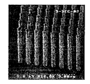
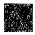
図1Aないし1Eに様々な方法を用いて製造された相異なる例示的な超疎水性表面を示す。具体的には、これらの図に、ナノポストおよび/またはマイクロポストとして知られる様々な直径および規則性の程度が様々な小さなポストを有する基板を示す。ナノポストおよびマイクロポストの例示的な製造方法は、その全体が本明細書に参照により組み込まれている、2001年2月13日に出願のトヌッキ(Tonucci)らの「ナノポスト・アレイおよびその作製方法(Nanopost arrays and process for making same)」という名称の米国特許第6,185,961号に見られる。ナノポストは、様々なリソグラフィ手段および様々なエッチング方法による鋳型の使用などの様々な方法によって製作されてきた。 FIGS. 1A through 1E show different exemplary superhydrophobic surfaces produced using various methods. Specifically, these figures show substrates having various small diameters and varying degrees of regularity, known as nanoposts and / or microposts. Exemplary fabrication methods for nanoposts and microposts are described in Tonucci et al., “Nanopost Arrays and Fabrication Methods” filed on February 13, 2001, which is incorporated herein by reference in its entirety. No. 6,185,961 entitled “Nanopost arrays and processes for making same”. Nanoposts have been fabricated by a variety of methods, such as using a mold with a variety of lithographic means and a variety of etching methods.
水などの液滴が、適切に設計されたナノ構造化またはマイクロ構造化フィーチャ・パターンを有する基板上に載置されるとき、この液滴が受ける流れ抵抗は、このようなナノ構造またはマイクロ構造を有さない基板に比べて大幅に減少する。このように適切に設計されたフィーチャ・パターンを有する表面は、ここで本明細書にその全体が参照により組み込まれるジェイ・キム(J.Kim)およびシー・ジェイ・キム(C.J.Kim)の「液滴ベースのマイクロ流体中の流れ抵抗を大幅に低下させるナノ構造化表面(Nanostructured Surfaces for Dramatic Reduction of Flow Resistance in Droplet−based Microfluidics)」というタイトルの文献、2002年1月、ネバダ州ラス・ベガス、MEMS IEEE会議479〜482頁、の主題である。この参考文献は、一般に、どのようにして所定のナノ構造フィーチャの表面を用いることによって、表面に接触する流体の流れ抵抗を大幅に低下させることができるかを説明している。具体的には、キム(Kim)の参考文献は、液体に接触する表面に微細なパターンを形成し、液体の表面張力の上述の原理を用いることによって、表面上に配設された液滴が図2に示すようにナノ構造化パターンの最上部上に担持される。図2を参照すると、(表面構造に応じた)適切な液体の液滴201の選択によって、液滴と下にある固体表面との間に接触せずに、ナノポスト203の最上部上に液滴201を浮遊させることができる。これによって、液滴と表面202の間の接触面積が極めて小さくなり(液滴は、各ポスト203の最上部でのみ接触する)、したがって流れ抵抗が低くなる。
When a droplet such as water is placed on a substrate having a suitably designed nanostructured or microstructured feature pattern, the flow resistance experienced by the droplet is such a nanostructure or microstructure Compared to a substrate that does not have a significant decrease. Surfaces with such well-designed feature patterns are hereby incorporated by reference herein in their entirety by J. Kim and C. J. Kim. Literature entitled "Nanostructured Surfaces for Dramatic Reduction of Flow Resistance in Droplet-based Microfluidics", 2002, Nevada, USA. • The subject of Vegas, MEMS IEEE Conference, pages 479-482. This reference generally explains how the surface of a given nanostructure feature can be used to significantly reduce the flow resistance of a fluid in contact with the surface. Specifically, Kim's reference describes the formation of a fine pattern on a surface in contact with a liquid, and using the above-described principle of the surface tension of the liquid, the droplets disposed on the surface It is carried on the top of the nanostructured pattern as shown in FIG. Referring to FIG. 2, by selection of an appropriate liquid droplet 201 (depending on surface structure), the droplet on the top of the
多くの用途において、図2の表面202などの所与のナノ構造またはマイクロ構造表面への図2の液滴201などの所与の液体の浸透を制御してこの液体に及ぼされる流れ抵抗ならびに固体表面のぬれ性を制御することができることが望ましい。図3Aおよび3Bに、電気ぬれを用いて液体のナノ構造化表面内への浸透を制御する本発明の原理による一実施形態を示す。このような電気ぬれは、その全内容が参照により本明細書に組み込まれている2003年3月31日に出願の「ナノ構造化またはマイクロ構造化表面上で液体の動きを制御する方法および装置(Method and Apparatus for Controlling the Movement of a Liquid on a Nanostructured or Microstructured Surface)」という名称の同時係属の米国出願第10/403159号の主題の一部である。図3Aを参照すると、上記で説明したように、導電性液体の液滴301が円錐状のナノポスト302のナノ構造フィーチャ・パターン上に配設されて、液滴301の表面張力が液滴をナノポスト302の上側部分に浮遊させるようにする。この構成では、液滴は各ナノポストの表面区域f1のみを覆う。ナノポスト302は、導電性基板303の表面によって担持される。液滴301は、電源305を有する基板303にリード線304を介して例示的に電気接続される。図4に例示的ナノポストをより詳細に示す。この図面において、ナノポスト302は、誘電材料の絶縁層などの材料401によって液体(図3A中の301)から電気絶縁される。このナノポストは、さらに、周知のフッ素重合体などの表面エネルギーの低い材料402によって液体から分離される。このような表面エネルギーの低い材料は、液体とナノポスト表面の間の適切な初期接触角を得ることを可能にする。2枚の分離した相異なる材料を使用する代わりに、表面エネルギーが十分に低く、絶縁性が十分に高い材料の単一層を使用できることは当業者には明白であろう。
In many applications, the flow resistance and solids exerted on this liquid by controlling the penetration of a given liquid such as
図3Bに、たとえば、導電性液滴301に低電圧(たとえば、10〜20ボルト)を印加することによって、液体301とナノポスト302の間に電圧差が生じることを示す。液体とナノポスト表面の間の接触角は減少し、液滴301は、十分に低い接触角でナノポスト302の表面に沿ってy方向に下降し、ナノポスト302のそれぞれを完全に囲み基板303の上側表面に接触するまでナノ構造フィーチャ・パターンに浸透する。この構成で液滴は各ナノポストの表面区域f2を覆う。f2>>f1なので液滴301とナノポスト302の間の全接触面積は比較的広く、したがって、液滴301が受ける流れ抵抗は図3Aの実施形態におけるよりも大きくなる。すなわち、図3Bに示すように、液滴301はフィーチャ・パターンから液滴301を押しのけるのに十分な別の力が無い場合はナノ構造フィーチャ・パターンに対して効果的に静止する。このような制御は、本明細書にその全体が参照により組み込まれている2003年3月31日に出願の、「ナノ構造化表面上で液体の移動を可変的に制御する方法および装置(Method And Apparatus For Variably Controlling The Movement Of A Liquid On A Nanostructured Surface)」という名称の同時係属の米国出願第10/403159号の主題の一部分である。
FIG. 3B shows that, for example, applying a low voltage (eg, 10-20 volts) to the
別の従来の試みでは、ナノポストまたはマイクロポストの代わりに独立セル型ナノ構造化またはマイクロ構造化表面が、1つまたは複数の表面のナノセルまたはマイクロセル内部の流体の圧力が減少するとこの表面上に配設された液体がこの表面に浸透し、それによって、たとえば、液滴の受ける流れ抵抗が増大するような方法で使用される。このような独立セル構造は、1つまたは複数のセル内部の圧を所望のレベル以上に増大させることによって、液体が、少なくとも部分的に、セルの外に出され元の未浸透の流れ抵抗の低い位置に戻る点で有利である。この方法によって、液滴が受ける流れ抵抗の所望のレベルを実現するために、液滴の表面内への浸透を変えることができる。このような可変な浸透は、やはり本明細書にその全体が参照により組み込まれている2003年9月30日に出願の「動的に調節可能なナノ構造化またはマイクロ構造化表面上の可逆的移行(Reversible Transitions on Dynamically Tunable Nanostructured or Microstructured Surfaces)」という名称の同時係属の米国出願第10/674,448号の主題の一部分である。
上記で説明したもののような従来の試みは、表面に接触している液体の流れ抵抗の低下または表面上のナノ構造間またはマイクロ構造間に液体を浸透させ、たとえば、この液体を下にある表面と接触させることに関与していた。しかし、本発明の発明者らは、このような流れ抵抗の低下またはこのような浸透の発生に加えて、ある状況において、液体または他の流体を、ナノ構造またはマイクロ構造を担持している基板を通過させることが望ましい場合があることに気が付いた。 Conventional attempts, such as those described above, reduce the flow resistance of the liquid in contact with the surface or infiltrate the liquid between nanostructures or microstructures on the surface, e.g. Was involved in contact with. However, the inventors of the present invention, in addition to such a decrease in flow resistance or the occurrence of such infiltration, in some situations, liquids or other fluids, substrates carrying nanostructures or microstructures Noticed that it may be desirable to pass through.
したがって、我々は、ナノ構造化基板がナノ構造間に配設された複数の基板開口を有する複数のナノ構造を備える方法および装置を発明した。所望の流体が基板に接触すると、この流体の少なくとも一部分がこれらの開口の少なくとも1つを通過することができる。第1実施形態では、上記で説明したような方法によって流体をナノ構造に浸透させることによってこの流体に開口を通過させる。第2の実施形態では、基板が可撓性基板であり、曲げ力または引っ張り力などの機械的な力を基板に与えるとき、ナノポスト間の距離または基板上のナノセルの直径が増大する。このような増大によって、所望の液体がナノポストまたはナノセルに浸透できるようになり、したがって基板開口を通過できるようになる。最後に、第3の実施形態では、上記で説明したように、水などの第1流体が基板上のナノ構造に浸透するのを妨げられ、他方、蒸気やガスなどの第2流体は基板中の開口を経由して基板を通過できる。 Accordingly, we have invented a method and apparatus comprising a plurality of nanostructures with a plurality of substrate openings with the nanostructured substrate disposed between the nanostructures. When the desired fluid contacts the substrate, at least a portion of the fluid can pass through at least one of these openings. In the first embodiment, the fluid is passed through the opening by infiltrating the nanostructures by the method as described above. In the second embodiment, when the substrate is a flexible substrate, the distance between the nanoposts or the diameter of the nanocells on the substrate increases when a mechanical force such as a bending force or a pulling force is applied to the substrate. Such an increase allows the desired liquid to penetrate the nanoposts or nanocells and thus pass through the substrate opening. Finally, in the third embodiment, as described above, the first fluid, such as water, is prevented from penetrating into the nanostructures on the substrate, while the second fluid, such as vapor or gas, is in the substrate. The substrate can be passed through the opening.
図5にバッテリ中の電解質流体がバッテリが活性化されるまで電極から離されている図3Aおよび図3Bの実施形態の一例を示す。このようなバッテリは、本明細書にその全体が参照により組み込まれている2004年3月18日出願の同時係属の米国特許出願第10/803,641号の主題の一部分である。図5中、バッテリ501は、格納壁503を有する筐体内に収容された電解質流体502を有する。この電解質流体502は正極507に接触しているが、ナノ構造化表面507によって負極508から離されている。ナノ構造化表面507は負極の表面であってもよいし、あるいは、負極にボンディングされた表面でもよい。当業者なら、ナノ構造化表面をまた、正極に付随して使用して同様な有利な結果が得られることが判るであろう。図5では、電解質流体が、図3Aの液滴と類似の、表面のナノポストの最上部上に浮遊している。バッテリ501は、たとえば、負荷506を有する電気回路505中に挿入される。電解質流体502が負極に接触していないときは、電解質とバッテリ501の電極504および508との間に実質的に反応が生じない。
FIG. 5 shows an example of the embodiment of FIGS. 3A and 3B where the electrolyte fluid in the battery is separated from the electrodes until the battery is activated. Such a battery is part of the subject matter of co-pending US patent application Ser. No. 10 / 803,641, filed Mar. 18, 2004, which is hereby incorporated by reference in its entirety. In FIG. 5, the
図6に電気回路505内に挿入された図5のバッテリを示すが、上記で説明した電気ぬれの原理を利用してナノ構造化表面507に電圧を印加して、それによって、電解質流体502を表面507に浸透させ、負極508に電気接触させる。当業者ならこの電圧は、たとえば、バッテリに1つまたは複数のRFエネルギーのパルスを通過させることによって、任意の数の電源から発生させることができることが判るであろう。電解質のナノ構造中への浸透が生じるとき、電子は、上記で説明したように回路505を通って方向601に流れ始め、負荷506に電力が供給される。
FIG. 6 shows the battery of FIG. 5 inserted into the
一般的に定義されるように、「ナノ構造」は1マイクロメートル未満の少なくとも1つの次元を有する所定の構造であり、「マイクロ構造」は1ミリメートル未満の少なくとも1つの次元を有する所定の構造である。しかし、開示される実施形態はナノ構造およびナノ構造化表面に言及するが、多くの場合にマイクロ構造で置き換えることができることは本発明の発明者らによって企図されており、当業者には明白であろう。したがって、本発明の発明者らは、ここではナノ構造を1マイクロメートル未満の少なくとも1つの次元を有する構造ならびに1ミリメートル未満の少なくとも1つの次元を有する構造のどちらも含むものと定義する。「フィーチャ・パターン」という用語はマイクロ構造かまたはナノ構造のどちらかを指す。さらに、「液体」、「液滴(droplet)」、および「液滴(liquid droplet)」の用語は本明細書では同義的に使用される。これらの用語は、液滴の形状をしていてもいなくても液体または液体の一部分を指す。 As generally defined, a “nanostructure” is a predetermined structure having at least one dimension less than 1 micrometer, and a “microstructure” is a predetermined structure having at least one dimension less than 1 millimeter. is there. However, although the disclosed embodiments refer to nanostructures and nanostructured surfaces, it is contemplated by the inventors of the present invention that in many cases can be replaced by microstructures and will be apparent to those skilled in the art. I will. Accordingly, the inventors of the present invention define herein nanostructures to include both structures having at least one dimension less than 1 micrometer as well as structures having at least one dimension less than 1 millimeter. The term “feature pattern” refers to either a microstructure or a nanostructure. Further, the terms “liquid”, “droplet”, and “liquid droplet” are used interchangeably herein. These terms refer to a liquid or a portion of a liquid, whether or not in the form of a droplet.
図7Aおよび7Bはそれぞれナノセル・アレイの立体図および上面断面図である。上記で本明細書に組み込んだ‘641号出願に記載されているように、このようなナノセル・アレイが図5中の電解質流体502などの液体のナノ構造化表面507の内と外への可逆的浸透を実現するために使用することができる。具体的には、ナノポストの代わりにいくつかの独立セル701、ここでは具体例として六角形断面のセルが、図7Aおよび7Bに使用される。各セルはセルの内壁に沿って配設された、たとえば、電極702を有することができる。本明細書で用いられるように、独立セルという用語は、電解液などの液体が配設されるようにされた側を除き全ての側面が囲まれるセルとして定義される。このような独立セルはそのセル中に配設された液体を、たとえば、セル内部の圧力を増大させることによってセルから排出することができるという点で有利である。当業者なら、同等に有効な独立セル構成を実現するために、同等に有利な多くのセルの構成および幾何形状が可能であることが判るであろう。
7A and 7B are a three-dimensional view and a top cross-sectional view, respectively, of a nanocell array. As described in the '641 application incorporated herein above, such a nanocell array is reversible into and out of a liquid
本明細書において上述したもののような従来のナノ構造化表面は、一般に、図5および6のバッテリの実施形態の場合のように、ナノ構造上に配設された液体の流れ抵抗を低下させるため、および/または液体を所望の時間ナノ構造に浸透させ、下にある基板に接触させるために使用されてきた。しかし、本発明の発明者らは、多くの用途において、液体を選択的にナノ構造がその上に配設される下にある基板中を通過させることが望ましいことを発見した。このように液体を選択的に通過させるこのような表面の1つを図8に示す。具体的に、図8に、本発明の原理によるナノ構造化表面801を示すが、そこには下にある基板803を通過する複数の開口802がこの基板上のナノ構造804間に配設される。このナノ構造、ここではナノポストは、たとえば、直径300nmで高さ7ミクロンであり、開口は、たとえば、直径2ミクロンである。図8に示したものと類似の表面の様々な用途に多くの適切な寸法を選択できることは当業者なら判るであろう。同様に、ナノ構造は、ポリマー材料から製作された基板などの多くの適切な基板上に載置することができることも当業者なら判るであろう。したがって、本明細書において上記で構成し論じたように、液体が、図3Aに示すようなナノ構造上に配設されるとき、この液体はナノ構造に浸透しない。しかし、液体がナノ構造に浸透させられ下にある基板803に接触させられるとき、この液体は、図3Bに示す例と同様に基板の開口を通過するであろう。
Conventional nanostructured surfaces such as those described hereinabove generally reduce the flow resistance of the liquid disposed on the nanostructure, as in the battery embodiment of FIGS. And / or liquids have been used to infiltrate the nanostructure for a desired time and contact the underlying substrate. However, the inventors of the present invention have found that in many applications it is desirable to selectively pass liquids through an underlying substrate on which nanostructures are disposed. One such surface that selectively allows liquid to pass through is shown in FIG. Specifically, FIG. 8 shows a
図9に、本発明の原理による図5に示したものと同様な、開口を有する表面が有利に使用されるバッテリの例示的な一実施形態を示す。図5を参照すると、具体的には、‘641号出願においてより完全に説明されるように、この図に表されたバッテリは、電極、たとえば、図5の負電極508の1つの表面上に複数のナノ構造を配設することによって部分的に製作される。しかし、このような電極上へのナノ構造の配設は、処理の難しさ、またはこのような表面の製造に伴うコストのため、望ましくないことがある。したがって、本発明の発明者らは、たとえば、ナノ構造をその上に作製するのに潜在的に安価、かつ/または技術的に容易である材料から、分離したナノ構造化表面を製作することが望ましいことを見出した。
FIG. 9 illustrates an exemplary embodiment of a battery in which an apertured surface is advantageously used, similar to that shown in FIG. 5, in accordance with the principles of the present invention. Referring to FIG. 5, specifically, as described more fully in the '641 application, the battery represented in this figure is placed on one surface of an electrode, eg, the
したがって、図9に、どのようにして図8の表面がバッテリの用途内で使用され得るかを示す。具体的には、図9を参照すると電解質流体502がナノ構造によって電極508から再度分離される。しかし、電極508上に直接配設されるナノ構造の代わりに、図8に示すように、ナノ構造804が基板上803に配設され、基板803は、図8に示すように直接的にか、または間接的に電極508に取り付けられる。開口の寸法は、電解質がナノ構造804に浸透させられるとき、電解質は図2の開口802を通って基板803に浸透し、電極508に接触し、その結果、バッテリとの化学反応が開始するように選択される。‘641号出願により十分に説明されているように、ナノポストの代わりに図7Aおよび7Bのナノセルを使用してもよいことは当業者なら判るであろう。このような場合、図7のセル701は、例示的に製作することができナノセルの両端に開口を有する。あるいは、単一の開口が複数のセルにわたることもできる。すなわち、たとえば、図9の電極508にナノセル・アレイを取り付けるとき、ナノポストが使用された場合と同様な結果が得られるはずである。具体的には、液体電解質をナノセルに浸透させるとき、液体はセルのすべての通路を通過し、電極508に接触して、その結果、バッテリとの化学反応が開始するように選択する。電極がセルの一端を完全に覆い、その結果、一端が開放され他端が電極表面への取り付けのため完全に密封された独立セル・アレイを効果的に作製するような方法でナノセル・アレイを例示的に電極に取り付けることができる。したがって、上記および‘641号出願により十分に説明したように、たとえば、セル内の圧力を増大させることによって電解質を所望の時間にセルから排出することができる。
Accordingly, FIG. 9 illustrates how the surface of FIG. 8 can be used in battery applications. Specifically, referring to FIG. 9, the
図10に図8のナノ構造化表面801を用いる本発明の原理による別の実施形態を示す。具体的には、図10に示すように、液滴1001が表面801に接触するとき、この液滴がナノ構造804の先端部に配設されたままになって、下にある基板803の上に浮遊するように基板803を設計する。したがって、液滴1001はこのように配設されるので開口802を通過することはない。しかし、ある実装形態では、1002方向に移動する液体または流体を基板803を通過できるようにすることが望ましいことがある。たとえば、耐液体性で通気性の衣服をこのような表面から作ることができるはずである。具体的には、デラウェア州ニューアークのダブリュー・エル、ゴア・アンド・アソシエーツ(W.L.Gore & Associates)社によりゴアテックス(Goretex(登録商標))という登録商標名で製造され発売されている耐水性で通気性のフッ化ポリマー繊維とほとんど同じ方法で、図10に示す表面801を衣服の布の2層間に織り込みまたは他の方法で配設することができるはずである。このような衣服は、雨滴中の水などの液体がナノ構造に浸透するのを防ぎ、したがって下にある基板に浸透するのを防ぐ。すなわち、雨が方向1003に移動し衣服着用者の肌に届くのを妨ぐはずである。しかし、雨が繊維に浸透するのを防ぐことは望ましいが、一方で、着用者から蒸発された汗などの他の流体は反対方向1002に通過可能であることが望ましい。このような流体は、繊維中の開口1004を方向1002に容易に通過することができるはずである。したがって、耐水性で通気性の繊維がもたらされるはずである。
FIG. 10 illustrates another embodiment according to the principles of the present invention using the
当業者なら、たとえば高性能水着などの他の衣類の用途に、このような繊維を有利に使用できるはずであることが判るであろう。近年、たとえば、プロの泳者が水中を移動する際に受ける抵抗を下げることができる低抵抗水着について多くの研究がなされてきた。上記で説明したように、ナノ構造化表面の1つの利点は、適切な構成にするとき、水などの液体とナノ構造化表面の間に極めて低い流れ抵抗を作ることができることである。したがって、図8の表面801は、水着の外側繊維として使用するとき、泳者が水中を移動する際、流れ抵抗を低くし、同時に、先に論じたように汗が繊維から出て行くことを可能にする。
One skilled in the art will appreciate that such fibers could be advantageously used in other garment applications such as high performance swimwear. In recent years, for example, many studies have been made on low-resistance swimsuits that can reduce the resistance experienced by professional swimmers when they move underwater. As explained above, one advantage of nanostructured surfaces is that when properly configured, a very low flow resistance can be created between a liquid such as water and the nanostructured surface. Thus, the
図11に、本発明の原理による別の実施形態を示すが、この場合、表面が曲げ力や引っ張り力などの機械的な力を受けるとき、液体がこの表面のナノ構造に浸透可能になるはずである。具体的には、基板1102のナノ構造化表面1108を可撓性ポリマー材料から製作する。本明細書の教示に鑑みて、様々なポリマー材料がこの目的のために役立つことは当業者には明らかであろう。図11Aを参照すると、ナノ構造1101の最上部、ここではナノポストが距離1105だけ離されている。先に論じたように、図11Aを参照すると、適切に選択された液体の液滴1104がナノ構造1101上に配設されるとき、液滴はこの構造の最上部に静止し、基板1102の上を浮遊する。しかし、図11Bを参照すると、表面が1109方向に曲げられまたは引き伸ばされるとき、ナノ構造1101間の分離距離が距離1106まで増大する。したがって、この液体の表面張力は、液体に応じて変わる特定の分離間隔で、ナノ構造1101の先端部上に液体を保持するには不十分になるであろう。したがって、液体1104は、この特定の分離間隔でナノ構造1101間の1107方向に移動し基板に接触するであろう。先に論じたように、液体1104が基板1102に接触するとき、開口1103はこの液体の少なくとも一部分をこの基板を通過できるようにする。
FIG. 11 illustrates another embodiment in accordance with the principles of the present invention, in which case the liquid should be able to penetrate the nanostructures of this surface when the surface is subjected to mechanical forces such as bending and pulling forces. It is. Specifically, the
図11Aおよび11Bに示されたナノ構造化表面は、たとえば、液体を保持するように意図された容器に有用なことがある。具体的には、図11Aの表面1108などの表面をこのような容器の1つまたは複数の壁面の一部分に使用することができるはずである。この容器内の圧力が所望の圧力以下のとき、液体はナノ構造に担持され、したがって液体はこの表面を通過しないであろう。しかし、容器内の圧力が、所定のレベルになるとき、図11Bの例のように、この表面は伸びナノ構造間の間隔は変わるであろう。すなわち、液体は、表面が引き伸ばされずナノ構造間の間隔の少なくとも一部分が復元される点まで、容器内の圧力が低下するまでナノ構造化表面を通過するであろう。このようにして、液体保持容器内の圧力を所望の圧力以下に維持することができる。
The nanostructured surface shown in FIGS. 11A and 11B may be useful, for example, for containers intended to hold liquids. Specifically, a surface such as
前記のことは本発明の単なる例示にすぎない。すなわち、当然のことながら、本明細書ではっきりと説明または図示していないが、本発明の原理に当てはまりその精神および範疇内にある様々な構成を当業者なら考案できるであろう。たとえば、本明細書の様々な実施形態の説明に鑑みて、当業者なら、本発明の原理が本質的に異なる技術分野および用途に幅広く使用できることが判るであろう。たとえば、本明細書で開示された透過性のナノ構造化表面を、燃料を所望の時間残りのシステムと分離させる故に燃料電池に有利に使用することができるはずであることは当業者なら判るであろう。当業者には他の用途も幅広く理解できるであろう。 The foregoing is merely illustrative of the invention. That is, it should be understood that those skilled in the art will be able to devise various configurations that fall within the spirit and scope of the principles of the invention but are not explicitly described or illustrated herein. For example, in light of the description of various embodiments herein, one of ordinary skill in the art will appreciate that the principles of the present invention can be widely used in essentially different technical fields and applications. For example, those skilled in the art will appreciate that the permeable nanostructured surface disclosed herein could be advantageously used in fuel cells to separate the fuel from the rest of the system for the desired time. I will. Other applications will be widely understood by those skilled in the art.
本明細書で列挙した全ての例または条件的な言い回しは、明らかに、読者が本発明の原理を理解するのを支援する教育的な目的のためだけに意図されており、このような具体的に列挙した例および条件に限定するものではないと解釈すべきである。さらに、本明細書で本発明の態様および実施形態を列挙している全ての記述ならびにその具体例は、それらと機能的に同等なものを包含するものとする。 All examples or conditional phrases listed herein are clearly intended solely for educational purposes to assist the reader in understanding the principles of the invention, and such specific It should not be construed as being limited to the examples and conditions listed in. Furthermore, all descriptions and specific examples listing aspects and embodiments of the invention herein are intended to include functional equivalents thereof.
Claims (10)
前記基板の表面上に配設された複数のナノ構造体であって、流体を該表面の上方に、該表面に接触させることなく保持することができる適切に設計されたフィーチャー・パターンを有する複数のナノ構造体からなり、
前記流体及び/又は前記基板に付加された電気的または機械的な力により前記流体が選択的に前記複数のナノ構造体に浸透し前記基板に接触するときに該流体の少なくとも一部分が前記複数の開口部を貫流するように、該複数の開口部が該複数のナノ構造体中の少なくとも一部分のナノ構造体間に配設された装置。 A substrate having a plurality of openings, and a plurality of nanostructures disposed on the surface of the substrate, wherein fluid can be retained above the surface without contacting the surface. Consisting of multiple nanostructures with designed feature patterns,
At least a portion of said plurality of fluid when in contact with the substrate penetrates into the fluid and / or electrical added to the substrate or mechanical said plurality of nanostructures said fluid selectively by the force An apparatus wherein the plurality of openings are disposed between at least a portion of the nanostructures in the plurality of nanostructures so as to flow through the openings.
前記ナノ構造体に関する寸法が変化するような方法で前記基板の形状を変形させるステップからなり、
前記寸法が変化すると、前記ナノ構造体上に配設された液体が、前記複数のナノ構造体に浸透し、前記複数の開口部の少なくとも一部分を貫流する、方法。 A method of using with a substrate having a plurality of disposed nanostructures thereon, wherein the substrate has a plurality of openings disposed between at least a portion of the structures in the plurality of nanostructures. In addition,
Deforming the shape of the substrate in such a way that the dimensions for the nanostructures change,
The method, wherein when the dimension changes, a liquid disposed on the nanostructure penetrates the plurality of nanostructures and flows through at least a portion of the plurality of openings.
Applications Claiming Priority (2)
| Application Number | Priority Date | Filing Date | Title |
|---|---|---|---|
| US10/835639 | 2004-04-30 | ||
| US10/835,639 US7323033B2 (en) | 2004-04-30 | 2004-04-30 | Nanostructured surfaces having variable permeability |
Publications (3)
| Publication Number | Publication Date |
|---|---|
| JP2005349558A JP2005349558A (en) | 2005-12-22 |
| JP2005349558A5 JP2005349558A5 (en) | 2008-04-03 |
| JP5031199B2 true JP5031199B2 (en) | 2012-09-19 |
Family
ID=34940859
Family Applications (1)
| Application Number | Title | Priority Date | Filing Date |
|---|---|---|---|
| JP2005128793A Expired - Fee Related JP5031199B2 (en) | 2004-04-30 | 2005-04-27 | Nanostructured surface with variable transmittance |
Country Status (7)
| Country | Link |
|---|---|
| US (2) | US7323033B2 (en) |
| EP (1) | EP1591415B1 (en) |
| JP (1) | JP5031199B2 (en) |
| KR (1) | KR101216979B1 (en) |
| CN (1) | CN1693189B (en) |
| CA (1) | CA2499595A1 (en) |
| DE (1) | DE602005000397T2 (en) |
Families Citing this family (43)
| Publication number | Priority date | Publication date | Assignee | Title |
|---|---|---|---|---|
| US7698550B2 (en) * | 2002-11-27 | 2010-04-13 | Microsoft Corporation | Native wi-fi architecture for 802.11 networks |
| US7557433B2 (en) | 2004-10-25 | 2009-07-07 | Mccain Joseph H | Microelectronic device with integrated energy source |
| US7227235B2 (en) * | 2003-11-18 | 2007-06-05 | Lucent Technologies Inc. | Electrowetting battery having a nanostructured electrode surface |
| KR20050093018A (en) * | 2004-03-18 | 2005-09-23 | 한국과학기술연구원 | Efficient 3-d nanostructured membranes |
| US7323033B2 (en) * | 2004-04-30 | 2008-01-29 | Lucent Technologies Inc. | Nanostructured surfaces having variable permeability |
| US7459121B2 (en) * | 2004-07-21 | 2008-12-02 | Florida State University Research Foundation | Method for continuous fabrication of carbon nanotube networks or membrane materials |
| CN100528382C (en) * | 2005-05-28 | 2009-08-19 | 鸿富锦精密工业(深圳)有限公司 | Nanometer screening device |
| US20070259156A1 (en) * | 2006-05-03 | 2007-11-08 | Lucent Technologies, Inc. | Hydrophobic surfaces and fabrication process |
| US7449649B2 (en) * | 2006-05-23 | 2008-11-11 | Lucent Technologies Inc. | Liquid switch |
| US8047235B2 (en) * | 2006-11-30 | 2011-11-01 | Alcatel Lucent | Fluid-permeable body having a superhydrophobic surface |
| US20090042065A1 (en) * | 2007-08-10 | 2009-02-12 | Mphase Technologies, Inc. | Event Activated Micro Control Devices |
| US20090042066A1 (en) * | 2007-08-10 | 2009-02-12 | Mphase Technologies, Inc. | Adjustable Barrier For Regulating Flow Of A Fluid |
| WO2009070796A1 (en) * | 2007-11-29 | 2009-06-04 | President And Fellows Of Harvard College | Assembly and deposition of materials using a superhydrophobic surface structure |
| US8435397B2 (en) * | 2008-01-25 | 2013-05-07 | Mphase Technologies, Inc. | Device for fluid spreading and transport |
| US20090191409A1 (en) * | 2008-01-25 | 2009-07-30 | Steve Simon | Combined Wetting/Non-Wetting Element For Low and High Surface Tension Liquids |
| US9039900B2 (en) * | 2008-05-09 | 2015-05-26 | New Jersey Institute Of Technology | Membrane distillation apparatus and methods |
| US11786036B2 (en) | 2008-06-27 | 2023-10-17 | Ssw Advanced Technologies, Llc | Spill containing refrigerator shelf assembly |
| US8286561B2 (en) | 2008-06-27 | 2012-10-16 | Ssw Holding Company, Inc. | Spill containing refrigerator shelf assembly |
| US7993524B2 (en) * | 2008-06-30 | 2011-08-09 | Nanoasis Technologies, Inc. | Membranes with embedded nanotubes for selective permeability |
| AU2009302806B9 (en) | 2008-10-07 | 2015-10-01 | Ross Technology Corporation | Highly durable superhydrophobic, oleophobic and anti-icing coatings and methods and compositions for their preparation |
| WO2010096072A1 (en) | 2009-02-17 | 2010-08-26 | The Board Of Trustees Of The University Of Illinois | Methods for fabricating microstructures |
| US20120052241A1 (en) * | 2009-02-17 | 2012-03-01 | The Board Of Trustees Of The University Of Illinoi S | Flexible Microstructured Superhydrophobic Materials |
| US9074778B2 (en) | 2009-11-04 | 2015-07-07 | Ssw Holding Company, Inc. | Cooking appliance surfaces having spill containment pattern |
| KR101636907B1 (en) * | 2009-12-08 | 2016-07-07 | 삼성전자주식회사 | Porous nano structure and Manufacturing Method of the same |
| EP2547832A4 (en) | 2010-03-15 | 2016-03-16 | Ross Technology Corp | Plunger and methods of producing hydrophobic surfaces |
| US9624101B2 (en) * | 2010-10-21 | 2017-04-18 | Hewlett-Packard Development Company, L.P. | Article with controlled wettability |
| BR112013021231A2 (en) | 2011-02-21 | 2019-09-24 | Ross Tech Corporation | superhydrophobic and oleophobic coatings with low voc bonding systems |
| DE102011085428A1 (en) | 2011-10-28 | 2013-05-02 | Schott Ag | shelf |
| DE102011121018A1 (en) * | 2011-12-13 | 2013-06-13 | Sartorius Stedim Biotech Gmbh | Hydrophobic or oleophobic microporous polymer membrane with structurally induced Abperl effect |
| WO2013090939A1 (en) | 2011-12-15 | 2013-06-20 | Ross Technology Corporation | Composition and coating for superhydrophobic performance |
| US9492578B2 (en) * | 2012-05-11 | 2016-11-15 | President And Fellows Of Harvard College | Reconfigurable surfaces for information security and protection of physical biometrics |
| AU2013281220B2 (en) | 2012-06-25 | 2017-03-16 | Ross Technology Corporation | Elastomeric coatings having hydrophobic and/or oleophobic properties |
| US20140238645A1 (en) | 2013-02-25 | 2014-08-28 | Alcatel-Lucent Ireland Ltd. | Hierarchically structural and biphillic surface energy designs for enhanced condensation heat transfer |
| US20140238646A1 (en) | 2013-02-25 | 2014-08-28 | Alcatel-Lucent Ireland Ltd. | Sloped hierarchically-structured surface designs for enhanced condensation heat transfer |
| CN107074524B (en) * | 2014-07-18 | 2020-01-17 | 加利福尼亚大学董事会 | Apparatus and method for retaining gas in microfeatures on submerged surfaces |
| CN104729579B (en) * | 2014-11-24 | 2017-05-31 | 清华大学 | Fluid sensor and its measuring method based on micro nanometer fiber array |
| US10184266B1 (en) * | 2015-06-19 | 2019-01-22 | X Development Llc | Flexible sheet for forming a semi-rigid structure |
| CN109399548A (en) * | 2017-08-17 | 2019-03-01 | 南京理工大学 | A kind of device and preparation method thereof automatically replying stable ultra-hydrophobic state |
| US11372494B2 (en) * | 2017-11-01 | 2022-06-28 | Bvw Holding Ag | Microstructured phase interfacial device |
| CN107777761A (en) * | 2017-11-08 | 2018-03-09 | 江门市蓬江区鑫浩源科技有限公司 | A kind of electrolytic cleaning processing unit |
| WO2021255546A1 (en) * | 2020-06-19 | 2021-12-23 | 3M Innovative Properties Company | Contactor module and contactor panel including contactor module |
| KR102365765B1 (en) * | 2020-07-09 | 2022-02-22 | 울산과학기술원 | Nano trench switch |
| CN112973295B (en) * | 2021-03-18 | 2022-03-29 | 中国石油大学(北京) | Coalescence filter core with flowing back function |
Family Cites Families (37)
| Publication number | Priority date | Publication date | Assignee | Title |
|---|---|---|---|---|
| JPH02146576A (en) * | 1988-11-29 | 1990-06-05 | Fujitsu Ltd | Oil applying device for fixing device of recording device |
| JPH0332729A (en) * | 1989-06-30 | 1991-02-13 | Biomaterial Universe Kk | Filter membrane responding to temperature |
| US5651900A (en) * | 1994-03-07 | 1997-07-29 | The Regents Of The University Of California | Microfabricated particle filter |
| JP3791999B2 (en) * | 1997-03-24 | 2006-06-28 | 株式会社アドバンス | Liquid particle handling equipment |
| JPH1138336A (en) * | 1997-07-18 | 1999-02-12 | Fujitsu Ltd | Optical switching element |
| EP1135328A1 (en) * | 1998-12-02 | 2001-09-26 | Massachusetts Institute Of Technology | Integrated palladium-based micromembranes for hydrogen separation and hydrogenation/dehydrogenation reactions |
| US6185961B1 (en) | 1999-01-27 | 2001-02-13 | The United States Of America As Represented By The Secretary Of The Navy | Nanopost arrays and process for making same |
| WO2000050232A1 (en) * | 1999-02-25 | 2000-08-31 | Seiko Epson Corporation | Structure member excellent in water-repellency and manufacturing method thereof |
| WO2000076634A1 (en) * | 1999-06-11 | 2000-12-21 | Gas Separation Technology, Inc. | Porous gas permeable material for gas separation |
| US6602932B2 (en) | 1999-12-15 | 2003-08-05 | North Carolina State University | Nanoparticle composites and nanocapsules for guest encapsulation and methods for synthesizing same |
| EP1261862A2 (en) * | 2000-02-22 | 2002-12-04 | California Institute of Technology | Development of a gel-free molecular sieve based on self-assembled nano-arrays |
| US6689439B2 (en) * | 2000-03-08 | 2004-02-10 | Zbigniew S. Sobolewski | Micro-stud diffusion substrate for use in fuel cells |
| JP3581298B2 (en) * | 2000-04-27 | 2004-10-27 | シャープ株式会社 | Field emission type electron source array and method of manufacturing the same |
| US6893562B2 (en) * | 2000-05-05 | 2005-05-17 | Millipore Corporation | Underdrain for filtration membrane |
| US6569225B2 (en) * | 2000-12-07 | 2003-05-27 | Kimberly-Clark Worldwide, Inc. | Breathable barrier films containing cavated fillers |
| US6913697B2 (en) * | 2001-02-14 | 2005-07-05 | Science & Technology Corporation @ Unm | Nanostructured separation and analysis devices for biological membranes |
| WO2003016040A1 (en) | 2001-04-16 | 2003-02-27 | The Regents Of The University Of California | Membrane mimetic architectures on nanoporous materials |
| KR100447931B1 (en) | 2001-10-24 | 2004-09-08 | 한국화학연구원 | The super water-repellent organic/inorganic composite membrane |
| PL204021B1 (en) * | 2001-11-02 | 2009-12-31 | Cnt Spo & Lstrok Ka Z Ogranicz | Superhydrophobous coating |
| US7140495B2 (en) * | 2001-12-14 | 2006-11-28 | 3M Innovative Properties Company | Layered sheet construction for wastewater treatment |
| SE0201738D0 (en) * | 2002-06-07 | 2002-06-07 | Aamic Ab | Micro-fluid structures |
| US6977009B2 (en) * | 2002-08-07 | 2005-12-20 | Hewlett-Packard Development Company, L.P. | Metal coated polymer electrolyte membrane having a reinforcement structure |
| US7641863B2 (en) * | 2003-03-06 | 2010-01-05 | Ut-Battelle Llc | Nanoengineered membranes for controlled transport |
| US20040191127A1 (en) | 2003-03-31 | 2004-09-30 | Avinoam Kornblit | Method and apparatus for controlling the movement of a liquid on a nanostructured or microstructured surface |
| US7156032B2 (en) | 2003-08-22 | 2007-01-02 | Lucent Technologies Inc. | Method and apparatus for controlling friction between a fluid and a body |
| US8124423B2 (en) | 2003-09-30 | 2012-02-28 | Alcatel Lucent | Method and apparatus for controlling the flow resistance of a fluid on nanostructured or microstructured surfaces |
| US7227235B2 (en) | 2003-11-18 | 2007-06-05 | Lucent Technologies Inc. | Electrowetting battery having a nanostructured electrode surface |
| US8915957B2 (en) | 2004-03-11 | 2014-12-23 | Alcatel Lucent | Drug delivery stent |
| US7749646B2 (en) * | 2004-03-18 | 2010-07-06 | Alcatel-Lucent Usa Inc. | Reversibly-activated nanostructured battery |
| KR20050093018A (en) * | 2004-03-18 | 2005-09-23 | 한국과학기술연구원 | Efficient 3-d nanostructured membranes |
| US7048889B2 (en) | 2004-03-23 | 2006-05-23 | Lucent Technologies Inc. | Dynamically controllable biological/chemical detectors having nanostructured surfaces |
| US20050211505A1 (en) | 2004-03-26 | 2005-09-29 | Kroupenkine Timofei N | Nanostructured liquid bearing |
| US7108813B2 (en) * | 2004-03-30 | 2006-09-19 | The Board Of Trustees Of The Leland Stanford Junior University | Gas/ion species selective membrane supported by multi-stage nano-hole array metal structure |
| US7005593B2 (en) | 2004-04-01 | 2006-02-28 | Lucent Technologies Inc. | Liquid electrical microswitch |
| US7323033B2 (en) | 2004-04-30 | 2008-01-29 | Lucent Technologies Inc. | Nanostructured surfaces having variable permeability |
| US7390760B1 (en) * | 2004-11-02 | 2008-06-24 | Kimberly-Clark Worldwide, Inc. | Composite nanofiber materials and methods for making same |
| KR20050074283A (en) * | 2004-12-27 | 2005-07-18 | 진텍, 인크. | Fabrication and activation processes for nanostructure composite field emission cathodes |
-
2004
- 2004-04-30 US US10/835,639 patent/US7323033B2/en active Active
-
2005
- 2005-03-07 CA CA002499595A patent/CA2499595A1/en not_active Abandoned
- 2005-04-15 EP EP05252369A patent/EP1591415B1/en not_active Expired - Fee Related
- 2005-04-15 DE DE602005000397T patent/DE602005000397T2/en active Active
- 2005-04-22 KR KR1020050033475A patent/KR101216979B1/en not_active IP Right Cessation
- 2005-04-27 JP JP2005128793A patent/JP5031199B2/en not_active Expired - Fee Related
- 2005-04-29 CN CN2005100684331A patent/CN1693189B/en not_active Expired - Fee Related
-
2006
- 2006-07-28 US US11/460,901 patent/US7695550B2/en active Active
Also Published As
| Publication number | Publication date |
|---|---|
| JP2005349558A (en) | 2005-12-22 |
| EP1591415B1 (en) | 2007-01-03 |
| CN1693184A (en) | 2005-11-09 |
| CA2499595A1 (en) | 2005-10-30 |
| DE602005000397T2 (en) | 2007-11-08 |
| KR101216979B1 (en) | 2013-01-02 |
| US20060255171A1 (en) | 2006-11-16 |
| US20050269743A1 (en) | 2005-12-08 |
| EP1591415A3 (en) | 2005-11-16 |
| US7323033B2 (en) | 2008-01-29 |
| EP1591415A2 (en) | 2005-11-02 |
| KR20060047398A (en) | 2006-05-18 |
| US7695550B2 (en) | 2010-04-13 |
| DE602005000397D1 (en) | 2007-02-15 |
| CN1693189B (en) | 2012-01-11 |
Similar Documents
| Publication | Publication Date | Title |
|---|---|---|
| JP5031199B2 (en) | Nanostructured surface with variable transmittance | |
| JP4965799B2 (en) | Method and apparatus for controlling fluid flow resistance on nanostructured or microstructured surfaces | |
| Yong et al. | Nature-inspired superwettability achieved by femtosecond lasers | |
| Yong et al. | A review of femtosecond‐laser‐induced underwater superoleophobic surfaces | |
| Guo et al. | Superhydrophobic surfaces: from natural to biomimetic to functional | |
| AU2002353905B2 (en) | Programmable surface control devices and method of making same | |
| US20190148321A1 (en) | Integration and bonding of micro-devices into system substrate | |
| Yong et al. | Underwater gas self-transportation along femtosecond laser-written open superhydrophobic surface microchannels (< 100 µm) for bubble/gas manipulation | |
| US20090317590A1 (en) | Method for fabricating superhydrophobic surface and solid having superhydrophobic surface structure by the same method | |
| US20100221597A1 (en) | Reversibly-activated nanostructured battery | |
| JP6773638B2 (en) | Devices and methods for retaining gas in microfeatures on the surface of the liquid | |
| JP2004111296A (en) | Microswitch and its manufacturing method | |
| Grigoryev et al. | Colloidal occlusion template method for micromanufacturing of omniphobic surfaces | |
| Li et al. | A review on fabrication and application of tunable hybrid micro–nano array surfaces | |
| EP2386596A1 (en) | Method for the production of polymeric membranes having an ordered arrangement of high-aspect-ratio nanopores, by means of heavy ion bombing | |
| JP2011513103A (en) | Method for producing a three-dimensional structure having a hydrophobic surface using metal foil | |
| Yanagishita et al. | Effect of Fine Structures Formed by Nanoimprinting Using Anodic Porous Alumina Mold on Surface Hydrophobicity | |
| US10927005B2 (en) | Method for manufacturing doubly re-entrant microstructures | |
| KR102059349B1 (en) | 3d nano structure manufacturing method and 3d nano device manufacturing method | |
| US20100247982A1 (en) | Reserve cell-array nanostructured battery | |
| Zheng et al. | Facile fabrication of sponge-like porous micropillar arrays via an electrochemical process | |
| Liu et al. | Silicon/polymer composite nanopost arrays | |
| KR101367561B1 (en) | Water-treatment membrane including metal nanotube and method for fabricating the same | |
| Kim et al. | Controlled patterning of vertical silicon structures using polymer lithography and wet chemical etching | |
| KR20150113471A (en) | The manufactoring method of fine metal mesh |
Legal Events
| Date | Code | Title | Description |
|---|---|---|---|
| A521 | Request for written amendment filed |
Free format text: JAPANESE INTERMEDIATE CODE: A523 Effective date: 20080214 |
|
| A621 | Written request for application examination |
Free format text: JAPANESE INTERMEDIATE CODE: A621 Effective date: 20080214 |
|
| A131 | Notification of reasons for refusal |
Free format text: JAPANESE INTERMEDIATE CODE: A131 Effective date: 20110202 |
|
| A601 | Written request for extension of time |
Free format text: JAPANESE INTERMEDIATE CODE: A601 Effective date: 20110502 |
|
| A602 | Written permission of extension of time |
Free format text: JAPANESE INTERMEDIATE CODE: A602 Effective date: 20110510 |
|
| A521 | Request for written amendment filed |
Free format text: JAPANESE INTERMEDIATE CODE: A523 Effective date: 20110802 |
|
| A131 | Notification of reasons for refusal |
Free format text: JAPANESE INTERMEDIATE CODE: A131 Effective date: 20110912 |
|
| A601 | Written request for extension of time |
Free format text: JAPANESE INTERMEDIATE CODE: A601 Effective date: 20111212 |
|
| A602 | Written permission of extension of time |
Free format text: JAPANESE INTERMEDIATE CODE: A602 Effective date: 20111215 |
|
| A521 | Request for written amendment filed |
Free format text: JAPANESE INTERMEDIATE CODE: A523 Effective date: 20120312 |
|
| TRDD | Decision of grant or rejection written | ||
| A01 | Written decision to grant a patent or to grant a registration (utility model) |
Free format text: JAPANESE INTERMEDIATE CODE: A01 Effective date: 20120530 |
|
| A01 | Written decision to grant a patent or to grant a registration (utility model) |
Free format text: JAPANESE INTERMEDIATE CODE: A01 |
|
| A61 | First payment of annual fees (during grant procedure) |
Free format text: JAPANESE INTERMEDIATE CODE: A61 Effective date: 20120627 |
|
| R150 | Certificate of patent or registration of utility model |
Free format text: JAPANESE INTERMEDIATE CODE: R150 |
|
| FPAY | Renewal fee payment (event date is renewal date of database) |
Free format text: PAYMENT UNTIL: 20150706 Year of fee payment: 3 |
|
| R250 | Receipt of annual fees |
Free format text: JAPANESE INTERMEDIATE CODE: R250 |
|
| LAPS | Cancellation because of no payment of annual fees |