JP5029190B2 - Reception circuit, electronic device, and noise canceling method - Google Patents
Reception circuit, electronic device, and noise canceling method Download PDFInfo
- Publication number
- JP5029190B2 JP5029190B2 JP2007192234A JP2007192234A JP5029190B2 JP 5029190 B2 JP5029190 B2 JP 5029190B2 JP 2007192234 A JP2007192234 A JP 2007192234A JP 2007192234 A JP2007192234 A JP 2007192234A JP 5029190 B2 JP5029190 B2 JP 5029190B2
- Authority
- JP
- Japan
- Prior art keywords
- signal
- unit
- phase shift
- amplification factor
- shift amount
- Prior art date
- Legal status (The legal status is an assumption and is not a legal conclusion. Google has not performed a legal analysis and makes no representation as to the accuracy of the status listed.)
- Expired - Fee Related
Links
Images


Classifications
-
- H—ELECTRICITY
- H04—ELECTRIC COMMUNICATION TECHNIQUE
- H04B—TRANSMISSION
- H04B1/00—Details of transmission systems, not covered by a single one of groups H04B3/00 - H04B13/00; Details of transmission systems not characterised by the medium used for transmission
- H04B1/38—Transceivers, i.e. devices in which transmitter and receiver form a structural unit and in which at least one part is used for functions of transmitting and receiving
- H04B1/3805—Transceivers, i.e. devices in which transmitter and receiver form a structural unit and in which at least one part is used for functions of transmitting and receiving with built-in auxiliary receivers
-
- H—ELECTRICITY
- H04—ELECTRIC COMMUNICATION TECHNIQUE
- H04B—TRANSMISSION
- H04B1/00—Details of transmission systems, not covered by a single one of groups H04B3/00 - H04B13/00; Details of transmission systems not characterised by the medium used for transmission
- H04B1/38—Transceivers, i.e. devices in which transmitter and receiver form a structural unit and in which at least one part is used for functions of transmitting and receiving
- H04B1/40—Circuits
- H04B1/50—Circuits using different frequencies for the two directions of communication
- H04B1/52—Hybrid arrangements, i.e. arrangements for transition from single-path two-direction transmission to single-direction transmission on each of two paths or vice versa
- H04B1/525—Hybrid arrangements, i.e. arrangements for transition from single-path two-direction transmission to single-direction transmission on each of two paths or vice versa with means for reducing leakage of transmitter signal into the receiver
Description
本発明は、受信回路、この受信回路を備えた電子機器及びノイズキャンセル方法に関する。 The present invention relates to a receiving circuit, an electronic device including the receiving circuit, and a noise canceling method.
ある回線に他の回線の信号が重畳する「クロストーク」と呼ばれる現象が知られており、漏話がその代表例である。クロストークは信号劣化の大きな要因になるため、クロストークを生じさせない、或いは混在したクロストーク成分を除去するための様々な技術が考案されている。その一例として、混在したクロストーク成分をキャンセル(減衰・除去)する信号(キャンセル信号)を生成して、クロストーク成分を除去する技術が知られている(例えば、特許文献1参照)。
ところで、受信回路を内蔵した電子機器においては、受信回路の近傍に配置されている電子回路の回路動作に伴う電磁場の変化に起因して交流信号が発生し、これが受信回路側に回り込んで妨害波として受信信号に混在してしまう場合がある。この場合、キャンセル信号を生成し受信信号に加算することで、受信信号に重畳した妨害波をキャンセルする、いわゆるノイズキャンセルの技術が知られている。 By the way, in an electronic device with a built-in receiver circuit, an AC signal is generated due to a change in the electromagnetic field due to the circuit operation of the electronic circuit arranged in the vicinity of the receiver circuit, and the AC signal circulates to the receiver circuit side and interferes therewith. In some cases, the received signal is mixed as a wave. In this case, a so-called noise cancellation technique is known in which a cancellation signal is generated and added to a reception signal to cancel an interference wave superimposed on the reception signal.
しかしながら、ノイズキャンセルが適切になされない場合があり得る。すなわち、妨害信号の検知の際に、例えば、妨害信号の一部のみが検知されたり、或いは妨害波に受信すべき信号の一部が混入された状態で検知されたりといったように、妨害波が正確に検知されない可能性があり、このような場合には、混入されている妨害波が殆ど除去されなかったり、或いは受信すべき信号の一部が減衰されてしまうといった事態が起こり得る。本発明は、上記事情に鑑みてなされたものであり、確実なノイズキャンセルの実現を目的としている。 However, noise cancellation may not be performed properly. That is, when detecting a jamming signal, for example, only a part of the jamming signal is detected, or a part of the signal to be received is mixed in the jamming wave, and the jamming wave is detected. There is a possibility that it cannot be detected accurately. In such a case, a mixed interference wave is hardly removed, or a part of a signal to be received may be attenuated. The present invention has been made in view of the above circumstances, and aims to realize reliable noise cancellation.
上記課題を解決するための第1の発明は、受信部近傍の妨害波を検出した信号或いは妨害信号そのものを入力し、所与の移相量及び振幅変更率で該入力した信号の位相及び振幅を可変して該信号を打ち消すキャンセル信号を生成するキャンセル信号生成部と、前記受信部で受信した受信信号に前記キャンセル信号を加算する加算部と、前記加算部により加算された信号を所与の増幅率で増幅する増幅部と、前記増幅された信号をデジタル信号に変換するA/D変換部と、前記変換されたデジタル信号が取り得る各信号値の頻度割合が既定の割合条件を満たすように前記増幅部の増幅率を可変に制御するAGC(Automatic Gain Control)部と、前記AGC部により可変される増幅率に基づいて、前記キャンセル信号生成部の移相量及び振幅変更率を可変に制御するキャンセル信号生成制御部とを備えた受信回路である。 According to a first aspect of the present invention for solving the above-described problems, a signal in which an interference wave in the vicinity of the receiving unit is detected or the interference signal itself is input, and the phase and amplitude of the input signal at a given phase shift amount and amplitude change rate. A cancel signal generator for generating a cancel signal for canceling the signal by changing the signal, an adder for adding the cancel signal to the received signal received by the receiver, and a signal added by the adder. An amplification unit that amplifies at an amplification factor, an A / D conversion unit that converts the amplified signal into a digital signal, and a frequency ratio of each signal value that can be taken by the converted digital signal so that a predetermined ratio condition is satisfied The AGC (Automatic Gain Control) unit that variably controls the amplification factor of the amplification unit, and the phase shift amount and the amplitude change rate of the cancellation signal generation unit are allowed based on the amplification factor that is variable by the AGC unit. It is a receiving circuit provided with the cancellation signal production | generation control part controlled strangely.
また、第8の発明は、前記受信部で受信した受信信号を所与の増幅率で増幅する増幅部と、前記増幅された信号をデジタル信号に変換するA/D変換部と、前記変換されたデジタル信号が取り得る各信号値の頻度割合が既定の割合条件を満たすように前記増幅部の増幅率を可変に制御するAGC(Automatic Gain Control)部とを備えた受信回路の前記受信信号に含まれるノイズ成分をキャンセルするノイズキャンセル方法であって、前記受信部近傍の妨害波を検出した信号或いは妨害信号そのものを入力し、所与の移相量及び振幅変更率で該入力した信号の位相及び振幅を可変して該信号を打ち消すキャンセル信号を生成することと、前記受信部で受信した受信信号に前記キャンセル信号を加算することと、前記増幅部に前記キャンセル信号が加算された前記受信信号を前記所与の増幅率で増幅させることと、前記AGC部により可変される増幅率に基づいて、前記キャンセル信号を生成する際の前記移相量及び振幅変更率を可変に制御することとを行うノイズキャンセル方法である。 Further, an eighth aspect of the invention relates to an amplification unit that amplifies the reception signal received by the reception unit at a given amplification factor, an A / D conversion unit that converts the amplified signal into a digital signal, and the converted signal. The reception signal of the reception circuit having an AGC (Automatic Gain Control) unit that variably controls the amplification factor of the amplification unit so that the frequency ratio of each signal value that can be taken by the digital signal satisfies a predetermined ratio condition. A noise canceling method for canceling included noise components, wherein a signal in which an interference wave in the vicinity of the receiving unit is detected or an interference signal itself is input, and the phase of the input signal with a given phase shift amount and amplitude change rate And generating a cancel signal that cancels the signal by varying the amplitude, adding the cancel signal to the received signal received by the receiving unit, and adding the cancel signal to the amplifying unit Amplifying the received signal with the given amplification factor, and variable the phase shift amount and amplitude change rate when generating the cancellation signal based on the amplification factor variable by the AGC unit This is a noise canceling method that performs control.
この第1の発明等によれば、受信信号にキャンセル信号を加算することで受信信号に含まれるノイズ成分がキャンセルされるとともに、受信信号にキャンセル信号を加算した信号を増幅する増幅部の増幅率に基づいて、キャンセル信号を生成する際の移相量及び振幅変更率が可変される。キャンセル信号の加算によるノイズの除去の程度は、このキャンセル信号の位相や振幅に応じて異なり、ノイズの除去の程度に応じて、受信信号にキャンセル信号が加算された後の信号のレベルが異なる。また、増幅部の増幅度は、A/D変換部により変換されたデジタル信号の各信号値の頻度割合が規定の割合条件を満たすように可変される。各信号値の頻度割合は、A/D変換部により変換される前の信号、すなわち増幅部により増幅された信号のレベルに応じて異なる。つまり、AGC部は、増幅部の増幅率を、増幅後の信号のレベルが一定となるように可変する。すなわち、キャンセル信号の位相や振幅が異なると、このキャンセル信号によるノイズ除去の程度が異なり、その結果、増幅部の増幅率が異なる。このため、キャンセル信号の生成の際の移相量や振幅変更率を増幅部の増幅率に基づいて可変することで、受信信号に含まれるノイズの除去に適切なキャンセル信号が生成され、適切なノイズキャンセルが実現される、 According to the first aspect of the invention, the noise component included in the received signal is canceled by adding the cancel signal to the received signal, and the amplification factor of the amplification unit that amplifies the signal obtained by adding the cancel signal to the received signal Based on the above, the phase shift amount and the amplitude change rate when generating the cancel signal are varied. The degree of noise removal by addition of the cancellation signal differs depending on the phase and amplitude of the cancellation signal, and the level of the signal after the cancellation signal is added to the reception signal differs depending on the degree of noise removal. In addition, the amplification degree of the amplification unit is varied so that the frequency ratio of each signal value of the digital signal converted by the A / D conversion unit satisfies a specified ratio condition. The frequency ratio of each signal value varies depending on the level of the signal before being converted by the A / D converter, that is, the signal amplified by the amplifier. That is, the AGC unit varies the amplification factor of the amplification unit so that the level of the amplified signal is constant. That is, when the phase and amplitude of the cancellation signal are different, the degree of noise removal by the cancellation signal is different, and as a result, the amplification factor of the amplification unit is different. For this reason, by changing the phase shift amount and amplitude change rate when generating the cancel signal based on the amplification factor of the amplification unit, a cancel signal suitable for removing noise included in the reception signal is generated, and an appropriate cancel signal is generated. Noise cancellation is realized,
第2の発明は、第1の発明の受信回路であって、前記キャンセル信号生成制御部は、前記キャンセル信号生成部の移相量及び振幅変更率を可変して、前記AGC部により可変された増幅率が最大となる移相量及び振幅変更率を検索し、前記キャンセル信号生成部の移相量及び振幅変更率とする検索処理を行う受信回路である。 2nd invention is the receiving circuit of 1st invention, Comprising: The said cancellation signal production | generation control part varied the phase shift amount and amplitude change rate of the said cancellation signal production | generation part, and was varied by the said AGC part This is a receiving circuit that searches for a phase shift amount and an amplitude change rate at which the amplification factor is maximized, and performs a search process using the phase shift amount and amplitude change rate of the cancel signal generation unit.
この第2の発明によれば、キャンセル信号の生成の際に、キャンセル信号の移相量及び振幅変更率を可変して増幅部の増幅率が最大となる移相量及び振幅変更率を検索し、移相量及び振幅変更率とする検索処理が行われる。 According to the second aspect of the invention, when the cancel signal is generated, the phase shift amount and the amplitude change rate of the amplifying unit are searched by changing the phase shift amount and the amplitude change rate of the cancel signal. A search process for setting the phase shift amount and the amplitude change rate is performed.
第3の発明は、第2の発明の受信回路であって、前記キャンセル信号生成制御部は、前記検索処理において前記AGC部により可変された増幅率が最大となった増幅率を含む増幅率変動許容範囲を設定し、前記検索処理の後は、前記AGC部により可変される増幅率が前記増幅率変動許容範囲内となるように前記キャンセル信号生成部の移相量及び振幅変更率を調整する調整処理を行う受信回路である。 A third invention is the receiving circuit according to the second invention, wherein the cancel signal generation control unit includes an amplification factor variation including an amplification factor at which the amplification factor varied by the AGC unit in the search process is maximized. An allowable range is set, and after the search process, the amount of phase shift and the amplitude change rate of the cancellation signal generation unit are adjusted so that the gain variable by the AGC unit is within the gain variation allowable range. It is a receiving circuit that performs adjustment processing.
この第3の発明によれば、検索処理の後は、増幅部の増幅率が、検索処理において可変された増幅率が最大となった増幅率を含む増幅率許容範囲内となるように、移相量及び振幅変更率を調整する調整処理が行われる。 According to the third aspect of the present invention, after the search process, the gain of the amplifying unit is shifted so as to be within the gain allowable range including the gain at which the gain varied in the search process is maximized. Adjustment processing for adjusting the phase amount and the amplitude change rate is performed.
第4の発明は、第3の発明の受信回路であって、前記キャンセル信号生成制御部は、前記調整処理中に前記AGC部によって可変された増幅率の大きさに基づいて、前記増幅率変動許容範囲を再設定する受信回路である。 A fourth invention is the receiving circuit according to the third invention, wherein the cancellation signal generation control unit is configured to change the gain variation based on the magnitude of the gain varied by the AGC unit during the adjustment process. This is a receiving circuit for resetting the allowable range.
この第4の発明によれば、調整処理中に可変された増幅部の増幅率の大きさに基づいて、増幅率変動許容範囲が再設定される。これにより、例えば受信信号に含まれるノイズの変動によって最適な増幅率が変動するといった場合であっても、増幅率変動許容範囲を再設定することで、より適切なノイズキャンセルが可能となる。 According to the fourth aspect of the present invention, the gain variation allowable range is reset based on the amplification factor magnitude varied during the adjustment process. As a result, even when the optimum amplification factor fluctuates due to fluctuations in noise included in the received signal, for example, more appropriate noise cancellation can be performed by resetting the amplification factor fluctuation allowable range.
第5の発明は、第3又は第4の発明の受信回路であって、前記キャンセル信号生成制御部が変更する前記キャンセル信号生成部の移相量及び振幅変更率の1回当たりの変更量が、前記検索処理よりも前記調整処理の方が小さい受信回路である。 A fifth invention is the receiving circuit of the third or fourth invention, wherein the amount of change per time of the phase shift amount and the amplitude change rate of the cancel signal generation unit changed by the cancel signal generation control unit is The receiving circuit is smaller in the adjustment process than in the search process.
この第5の発明によれば、キャンセル信号の生成の際の移相量及び振幅変更率の1回あたりの変更量は、検索処理よりも調整処理の方が小さい。 According to the fifth aspect of the present invention, the amount of phase shift and the amount of change of the amplitude change rate at the time of generating the cancel signal are smaller in the adjustment process than in the search process.
第6の発明は、第1〜第5の何れかの発明の受信回路であって、前記受信部は測位用衛星からの測位用衛星信号を受信し、前記A/D変換部により変換されたデジタル信号に基づいて現在位置を測位演算する測位演算部を備えた受信回路である。 A sixth invention is the receiving circuit according to any one of the first to fifth inventions, wherein the receiving unit receives a positioning satellite signal from a positioning satellite and is converted by the A / D conversion unit. It is a receiving circuit provided with a positioning calculation unit that calculates a current position based on a digital signal.
この第6の発明によれば、第1〜第5の何れかの発明の受信回路を、例えば測位用衛星からの測位用衛星信号としてGPS衛星からのGPS衛星信号を受信し、現在位置の測位演算を行うGPS受信回路に適用可能である。 According to the sixth invention, the receiving circuit according to any one of the first to fifth inventions receives a GPS satellite signal from a GPS satellite as a positioning satellite signal from, for example, a positioning satellite, and measures the current position. The present invention can be applied to a GPS receiving circuit that performs calculation.
第7の発明は、第1〜第6の何れかの発明の受信回路を備えた電子機器である。 A seventh invention is an electronic device including the receiving circuit according to any one of the first to sixth inventions.
この第7の発明によれば、第1〜第6の何れかの発明と同様の効果を奏する電子機器を実現できる。 According to the seventh aspect of the invention, it is possible to realize an electronic device that exhibits the same effects as any of the first to sixth aspects of the invention.
以下、図面を参照して、本発明の好適な実施形態を説明する。なお、以下では、本発明を、GPS機能を有する携帯電話機に適用した場合を説明するが、本発明の適用可能な実施形態がこれに限定されるものではない。 Hereinafter, preferred embodiments of the present invention will be described with reference to the drawings. In the following, a case where the present invention is applied to a mobile phone having a GPS function will be described, but embodiments to which the present invention can be applied are not limited thereto.
[携帯電話機の構成]
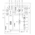
図1は、本実施形態の携帯電話機1の内部構成の一例を示すブロック図である。同図によれば、携帯電話機1は、GPS機能を有し、GPSアンテナ10と、受信回路であるGPS受信部20と、ホストCPU(Central Processing Unit)51と、操作部52と、表示部53と、ROM(Read Only Memory)54と、RAM(Random Access Memory)55と、携帯用無線通信回路部60と、携帯用アンテナ70とを備えて構成される。
[Configuration of mobile phone]
FIG. 1 is a block diagram illustrating an example of an internal configuration of the
GPSアンテナ10は、GPS衛星から送信されたGPS衛星信号を含むRF信号を受信するアンテナである。
The
GPS受信部20は、GPSアンテナ10で受信されたRF信号からGPS衛星信号を抽出し、GPS衛星信号から取り出した航法メッセージ等に基づく測位演算を行って現在位置を算出する。このGPS受信部20は、SAW(Surface Acoustic Wave)フィルタ21と、LNA(Low Noise Amplifier)22と、妨害波検知部23と、キャンセル信号生成部24と、加算器25と、RF(Radio Frequency)受信回路部30と、ベースバンド処理回路部40とを有している。なお、このGPS受信部20のうち、RF受信回路部30とベースバンド処理回路部40とは、それぞれ別のLSI(Large Scale Integration)として製造することも、1チップとして製造することも可能である。更に、SAWフィルタ21やLNA22等を含んだGPS受信部20全体を1チップとして製造することも可能である。
The
SAWフィルタ21は、バンドパスフィルタであり、GPSアンテナ10から入力されるRF信号に対して所定帯域の信号を通過させ、帯域外の周波数成分を遮断して出力する。LNA22は、低雑音アンプであり、SAWフィルタ21から入力される信号を増幅して出力する。
The
妨害波検知部23は、GPSアンテナ10により受信された受信信号に重畳される妨害波(ノイズ)を検知する。この妨害波検知部23は、受信部であるGPSアンテナ10やGPS受信部20の近傍の電磁場変化を検知するためのピックアップコイル等で構成され、検知した電磁場変化を妨害信号として出力する。なお、妨害波検知部23は、GPS受信部20内に配置せず、GPS受信部20外の任意の位置に設置可能とし、信号線等の配線でGPS受信部20と接続する構成としても良い。また、妨害波検知部23は、受信信号に重畳するノイズ(電磁場変化)を検知するものであり、電磁場変化の検知対象とする回路は何れの電子回路であっても良い。例えば、携帯電話機や無線LAN等の通信回路、CPU等のプロセッサ、液晶表示装置等の回路を検知対象とすることができる。但し、受信信号に対して妨害波となる電磁場変化を検知する必要があるため、GPSアンテナ10やGPS受信部20の近傍に位置する電子回路であることが望ましい。
The interference
キャンセル信号生成部24は、受信信号に重畳された妨害波を除去するためのキャンセル信号を生成する。すなわち、妨害波検知部23により検知された妨害信号を180度移相させた信号を、信号生成制御部43から入力されるキャンセル制御信号に従って、移相量φだけ移相させるとともに、減衰率α(振幅変更率)で減衰させてキャンセル信号を生成する。
The cancel
加算器25は、LNA22により増幅された信号に、キャンセル信号生成部24により生成されたキャンセル信号を加算する。
The
RF受信回路部30は、加算器25から入力される信号(RF信号)を中間周波数の信号(IF(Intermediate Frequency)信号)にダウンコンバートした後、デジタル信号に変換して出力する。このRF受信回路部30は、発振回路31と、ミキサ32と、増幅器33と、A/D変換器34とを有している。
The RF
発振回路31は、例えば水晶発振器であり、所定の発振周波数を有する局部発振信号を生成する。ミキサ32は、加算器25から入力されるRF信号と、発振回路31から入力される局部発振信号とを乗算(合成)してIF信号を生成する。増幅器33は、ミキサ32により生成されるIF信号を、AGC部42から入力されるゲイン制御信号に従って増幅度を可変して増幅する可変増幅器である。
The
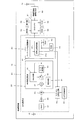
A/D変換器34は、増幅器33により増幅されたIF信号を、多ビット(2ビット以上)のデジタル信号に変換する。図2は、A/D変換器34によるA/D変換の原理を示す図であり、2ビット変換の場合を示している。この場合、3つの閾値TH1〜TH3(但し、TH1<TH2<TH3)が定められ、変換対象となるアナログ信号のレベルが何れの閾値TH間に位置するかに応じて、2ビットのデジタル信号(すなわち、「00」、「01」、「10」及び「11」)に変換される。
The A /
図2に戻り、ベースバンド処理回路部40は、RF受信回路部30から入力されるIF信号からGPS衛星信号を捕捉・追尾し、データを復号して取り出した航法メッセージや時刻情報等に基づいて擬似距離の算出演算や測位演算等を行う。また、このベースバンド処理回路部40は、CPU41と、ROM44と、RAM45とを有するとともに、レプリカコードの生成回路や相関演算を行う相関演算回路、データの復号回路等の各種回路を有している。
Returning to FIG. 2, the baseband
CPU41は、AGC部42と信号生成制御部43とを有し、ベースバンド処理回路部40の各部を統括的に制御するとともに、ベースバンド処理を含む各種演算処理を行う。ベースバンド処理では、RF受信回路部30から入力されたIF信号に基づくGPS衛星信号の捕捉・追尾を行う。GPS衛星信号の捕捉は、IF信号からGPS衛星信号を抽出する処理であり、IF信号に対する相関処理を行う。具体的には、IF信号と擬似的に発生させたレプリカコードとの相関を、FFT演算を用いて算出するコヒーレント処理を行い、このコヒーレント処理の結果である相関値を積算して相関積算値を算出するインコヒーレント処理を行う。これにより、GPS衛星信号に含まれるC/Aコード及び搬送波周波数の位相が得られる。
The
GPS衛星信号の追尾は、捕捉した複数のGPS衛星信号の同期保持を並列的に行う処理であり、例えば遅延ロックループ(DLL)で実現されてC/Aコードの位相を追尾するコードループと、例えば位相ロックループ(PLL)で実現されて搬送波周波数の位相を追尾するキャリアループとの処理を行う。そして、追尾した各GPS衛星信号のデータを復号して航法メッセージを取り出し、擬似距離の演算や測位演算等を行って現在位置を測位する処理を行う。 The tracking of GPS satellite signals is a process of performing synchronization holding of a plurality of captured GPS satellite signals in parallel. For example, a code loop that is realized by a delay lock loop (DLL) and tracks the phase of a C / A code; For example, processing is performed with a carrier loop that is realized by a phase lock loop (PLL) and tracks the phase of the carrier frequency. Then, the tracked GPS satellite signal data is decoded, a navigation message is extracted, and a process of positioning the current position by performing pseudorange calculation, positioning calculation, and the like is performed.
AGC部42は、RF受信回路部30から入力されるIF信号をもとに、増幅器33の増幅度を制御する。具体的には、A/D変換器34に変換されるデジタル信号の各信号値の割合が所定の割合条件を満たすように、増幅器33の増幅度を制御することで入力されるアナログ信号のレベルを制御する。この割合条件は、A/D変換器34における変換効率が最大効率となり得る条件であり、例えば、図2に示した2ビット変換の場合、変換された4つの信号値のうち、「10」と、「00」と、「11」及び「01」とのそれぞれの値の頻度割合が等しくなることである。
The
ところで、GPSアンテナ10で受信される受信信号は、受信すべき信号であるGPS衛星信号に妨害波(ノイズ)が混入(重畳)された信号である。すなわち、受信信号のレベルは、GPS衛星信号のレベルより、混入している妨害波のレベルの分だけ大きくなっているとともに、この妨害波のレベルは、その混入の程度によって変動する。つまり、AGC部42は、受信信号に混入する妨害波のレベルが大きくなるほど、ゲインを下げるように増幅器33の増幅度を制御することになる。
By the way, the reception signal received by the
信号生成制御部43は、AGC部42により算出されるゲインをもとに、キャンセル信号生成部24がキャンセル信号を生成する際の移相量φ及び減衰率αを制御するキャンセル制御信号を生成する。図3は、キャンセル信号の位相又は振幅に対するゲインのイメージを示す図である。受信信号に混入している妨害波の除去の程度は、キャンセル信号の位相及び振幅に応じて異なる。また、上述のように、AGC部42による増幅器33の増幅度の制御は、受信信号に混入される妨害波のレベルが大きいほど、ゲインを下げるように行われる。つまり、受信信号への妨害波の混入の程度が大きいほど、ゲインは小さくなる。つまり、図3に示すように、ゲインは、キャンセル信号の位相や振幅に応じて変動し、妨害波が最大限に除去されたときに最大となる。このため、信号生成制御部43は、ゲインが最大となるように、キャンセル信号生成部24におけるキャンセル信号の生成の際の移相量φ及び減衰率αを制御する。
Based on the gain calculated by the
具体的には、先ず、最大ゲインを検索する。すなわち、減衰率αを一定値とした状態で、移相量φを所定の移相変更量Δφ1ずつ増加或いは減少させることで可変して、ゲインが最大となる移相量φを探す。ゲインが最大となる移相量φを決定すると、次いで、移相量φをこの値に固定した状態で、減衰率αを所定の減衰率変更量Δα1ずつ増加或いは減少させることで可変して、ゲインが最大となる減衰率αを探す。 Specifically, first, the maximum gain is searched. That is, in a state where the attenuation rate α is a constant value, the phase shift amount φ is varied by increasing or decreasing by a predetermined phase shift change amount Δφ1 to search for the phase shift amount φ with the maximum gain. When the phase shift amount φ at which the gain is maximized is determined, the attenuation rate α is then varied by increasing or decreasing the predetermined attenuation rate change amount Δα1 in a state where the phase shift amount φ is fixed to this value, Find the attenuation rate α that maximizes the gain.
そして、ゲインが最大となる減衰率αを決定すると、このときのゲインを最大ゲインとみなし、最大ゲインを中心とした所定範囲を最大ゲイン範囲(増幅率変動許容範囲)として設定する。このとき、決定した最大ゲインは、必ずしも真の最大ゲインとは一致しない。これは、移相量φ及び減衰率αそれぞれを、変更量Δφ,Δαずつ変更しているためである。このため、最大ゲインを中心とする所定範囲を最大ゲイン範囲として設定する。 When the attenuation rate α at which the gain is maximized is determined, the gain at this time is regarded as the maximum gain, and a predetermined range centering on the maximum gain is set as the maximum gain range (amplification rate fluctuation allowable range). At this time, the determined maximum gain does not necessarily match the true maximum gain. This is because the phase shift amount φ and the attenuation rate α are changed by the change amounts Δφ and Δα, respectively. For this reason, a predetermined range centering on the maximum gain is set as the maximum gain range.
その後、ゲインがこの最大ゲイン範囲内に収まるように、移相量φ及び減衰率αを調整する。すなわち、現在のゲインが最大ゲイン範囲内ならば、現在の移相量φ及び減衰率αをそのまま保持する。そして、現在のゲインが最大ゲイン範囲外となったら、再度、移相量φ及び減衰率αを可変して、ゲインが最大ゲイン範囲内となるように調整する。すなわち、上述の最大ゲインの検索と同様に、移相量φ及び減衰率αの一方を固定し他方を可変して、最大ゲインとなる移相量φ及び減衰率αの値を探す。そして、そのときのゲインを新たな最大ゲインとみなし、最大ゲイン範囲を再設定する。このとき、移相量φ及び減衰率αそれぞれは所定の変更量Δφ2,Δα2ずつ変更する。この変更量Δφ2,Δα2は、最大ゲインの検索の際の変更量Δφ1,Δα1より小さく設定されている。 Thereafter, the phase shift amount φ and the attenuation rate α are adjusted so that the gain falls within this maximum gain range. That is, if the current gain is within the maximum gain range, the current phase shift amount φ and attenuation rate α are held as they are. When the current gain falls outside the maximum gain range, the phase shift amount φ and the attenuation rate α are changed again to adjust the gain to be within the maximum gain range. That is, similarly to the search for the maximum gain described above, one of the phase shift amount φ and the attenuation rate α is fixed and the other is varied to search for the value of the phase shift amount φ and the attenuation rate α that becomes the maximum gain. Then, the gain at that time is regarded as a new maximum gain, and the maximum gain range is reset. At this time, each of the phase shift amount φ and the attenuation rate α is changed by a predetermined change amount Δφ2, Δα2. The change amounts Δφ2 and Δα2 are set smaller than the change amounts Δφ1 and Δα1 when searching for the maximum gain.
ROM44は、CPU41がベースバンド処理回路部40及びRF受信回路部30の各部を制御するためのシステムプログラムや、ベースバンド処理を含む各種処理を実現するための各種プログラムやデータ、信号生成制御部43によるキャンセル信号生成制御処理を実現するための信号生成制御プログラム44a等を記憶している。
The
RAM45は、CPU41の作業領域として用いられ、ROM44から読み出されたプログラムやデータ、CPU41が各種プログラムに従って実行した演算結果等を一時的に記憶する。
The
ホストCPU51は、ROM54に記憶されているシステムプログラム等の各種プログラムに従って携帯電話機1の各部を統括的に制御する。具体的には、主に、電話機としての通話機能を実現するとともに、ベースバンド処理回路部40から入力された携帯電話機1の現在位置を地図上にプロットしたナビゲーション画面を表示部53に表示させるといったナビゲーション機能を含む各種機能を実現するための処理を行う。
The
操作部52は、操作キーやボタンスイッチ等により構成される入力装置であり、利用者による操作に応じた操作信号をホストCPU51に出力する。この操作部52の操作により、測位の開始/終了指示等の各種指示が入力される。表示部53は、LCD(Liquid Crystal Display)等により構成される表示装置であり、ホストCPU51から入力される表示信号に基づく表示画面(例えば、ナビゲーション画面や時刻情報等)を表示する。
The
ROM54は、ホストCPU51が携帯電話機1を制御するためのシステムプログラムや、ナビゲーション機能を実現するための各種プログラムやデータ等を記憶している。RAM55は、ホストCPU51の作業領域として用いられ、ROM54から読み出されたプログラムやデータ、操作部52から入力されたデータ、ホストCPU51が各種プログラムに従って実行した演算結果等を一時的に記憶する。
The
携帯用無線通信回路部60は、RF変換回路やベースバンド処理回路等によって構成される携帯電話用の通信回路部であり、ホストCPU51の制御に従って無線信号の送受信を行う。携帯用アンテナ70は、携帯電話機1の通信サービス事業者が設置した無線基地局との間で携帯電話用無線信号の送受信を行うアンテナである。なお、図示していないが、携帯用無線通信回路部60等の他の回路等でも、発振回路31により生成される基準信号REFが利用される。
The portable wireless
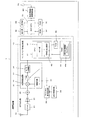
[処理の流れ]
図4は、信号生成制御部43による信号生成制御処理の流れを説明するためのフローチャートである。同図によれば、信号生成制御部43は、先ず、最大ゲインを探す検索処理を行う。すなわち、初期設定として、移相量φ及び減衰率αを定められた初期値に設定する(ステップA1)。また、移相変更量Δφ及び減衰率変更量Δαそれぞれを、定められた最大ゲイン検索用の変更量Δφ1,Δα1に設定する(ステップA3)。次いで、移相量/減衰率可変処理を行い、キャンセル信号の移相量φ及び減衰率αを可変して最大ゲインを検索する(ステップA5)。
[Process flow]
FIG. 4 is a flowchart for explaining the flow of signal generation control processing by the signal
図5は、移相量/減衰率可変処理の流れを説明するためのフローチャートである。同図によれば、現在のゲインを最大ゲインとして設定する(ステップB1)。次いで、減衰率αを固定としたまま、移相量φを移相変更量Δφだけ増加させる(ステップB3)。その結果、現在のゲインが最大ゲインを超えるならば(ステップB5:YES)、現在のゲインを最大ゲインとして再設定する(ステップB7)。その後、ステップB3に戻り、移相量φを更に増加させて同様の処理を繰り返す。一方、移相量φを増加させた結果、現在のゲインが最大ゲイン以下となったならば(ステップB5:NO)、移相量φを移相変更量Δφだけ減少させる(ステップB9)。その結果、現在のゲインが最大ゲインを超えるならば(ステップB11:YES)、現在のゲインを最大ゲインとして再設定する(ステップB13)。その後、ステップB9に戻り、移相量φを更に減少させて同様の処理を繰り返す。 FIG. 5 is a flowchart for explaining the flow of the phase shift amount / attenuation rate variable process. According to the figure, the current gain is set as the maximum gain (step B1). Next, the phase shift amount φ is increased by the phase shift change amount Δφ while the attenuation rate α is fixed (step B3). As a result, if the current gain exceeds the maximum gain (step B5: YES), the current gain is reset as the maximum gain (step B7). Thereafter, the process returns to step B3, and the same process is repeated by further increasing the phase shift amount φ. On the other hand, if the current gain becomes equal to or less than the maximum gain as a result of increasing the phase shift amount φ (step B5: NO), the phase shift amount φ is decreased by the phase shift change amount Δφ (step B9). As a result, if the current gain exceeds the maximum gain (step B11: YES), the current gain is reset as the maximum gain (step B13). Thereafter, the process returns to step B9, and the same process is repeated by further reducing the phase shift amount φ.
一方、移相量φを減少させた結果、現在のゲインが最大ゲイン以下となったならば(ステップB11:NO)、続いて、移相量φを固定としたまま、減衰率αを減衰率変更量Δαだけ増加させる(ステップB15)。その結果、現在のゲインが最大ゲインを超えるならば(ステップB17:YES)、現在のゲインを最大ゲインとして再設定する(ステップB19)。そして、ステップB15に戻り、減衰率αを更に増加させて同様の処理を繰り返す。一方、減衰率αを増加させた結果、現在のゲインが最大ゲイン以下となったならば(ステップB17:NO)、減衰率αを減衰率変更量Δαだけ減少させる(ステップB21)。その結果、現在のゲインが最大ゲインを超えるならば(ステップB23:YES)、現在のゲインを最大ゲインとして設定する(ステップB25)。その後、ステップB21に戻り、減衰率αを更に減少させて同様の処理を繰り返す。一方、減衰率αを減少させた結果、現在のゲインが最大ゲイン以下となったならば(ステップB23:NO)、移相量/減衰率可変処理を終了する。 On the other hand, if the current gain becomes equal to or less than the maximum gain as a result of decreasing the phase shift amount φ (step B11: NO), then the attenuation rate α is set to the attenuation rate while the phase shift amount φ is fixed. The change amount is increased by Δα (step B15). As a result, if the current gain exceeds the maximum gain (step B17: YES), the current gain is reset as the maximum gain (step B19). Then, returning to step B15, the attenuation rate α is further increased, and the same processing is repeated. On the other hand, if the current gain becomes equal to or less than the maximum gain as a result of increasing the attenuation rate α (step B17: NO), the attenuation rate α is decreased by the attenuation rate change amount Δα (step B21). As a result, if the current gain exceeds the maximum gain (step B23: YES), the current gain is set as the maximum gain (step B25). Thereafter, the process returns to step B21, and the attenuation rate α is further decreased, and the same processing is repeated. On the other hand, if the current gain becomes equal to or less than the maximum gain as a result of decreasing the attenuation rate α (step B23: NO), the phase shift amount / attenuation rate variable process is terminated.
移相量/減衰率可変処理が終了すると、この処理において最終的に設定された最大ゲインを中心とする所定範囲を最大ゲイン範囲として設定する(ステップA7)。ここまでが、検索処理である。 When the phase shift amount / attenuation rate variable process is completed, a predetermined range centered on the maximum gain finally set in this process is set as the maximum gain range (step A7). This is the search process.
検索処理が終了すると、続いて、最大ゲインを保持するようにキャンセル信号を調整する調整処理を行う。すなわち、移相変更量Δφ及び減衰率変更量Δαそれぞれを、定められた最大ゲインの保持用の変更量Δφ2,Δα2に設定する(ステップA9)。そして、AGC部42から入力される現在のゲインがこの最大ゲイン範囲内であるか否かを判断し、最大ゲイン範囲外であるならば(ステップA11:NO)、再度、移相量/減衰率可変処理(図5参照)を行い、キャンセル信号の移相量φ及び減衰率αを可変して最大ゲインを検索する(ステップA13)。移相量/減衰率可変処理を終了すると、設定された最大ゲインを中心とする所定範囲を最大ゲイン範囲として再設定する(ステップA15)。ここまでが、調整処理である。
When the search process is completed, an adjustment process for adjusting the cancel signal so as to maintain the maximum gain is subsequently performed. That is, the phase shift change amount Δφ and the attenuation rate change amount Δα are respectively set to the predetermined change amounts Δφ2, Δα2 for holding the maximum gain (step A9). Then, it is determined whether or not the current gain input from the
調整処理が終了すると、測位が終了であるか否かを判断し、終了しないならば(ステップA17:NO)、ステップA11に戻り、終了するならば(ステップA17:YES)、キャンセル信号制御処理を終了する。 When the adjustment process is finished, it is determined whether or not the positioning is finished. If not finished (step A17: NO), the process returns to step A11, and if finished (step A17: YES), the cancel signal control process is performed. finish.
[作用・効果]
このように、本実施形態によれば、GPS機能を有する携帯電話機1では、信号生成制御部43は、AGC部42により増幅度が可変制御される増幅器33のゲインをもとに、キャンセル信号生成部24におけるキャンセル信号の生成を制御する。具体的には、ゲインが最も大きくなるように、キャンセル信号を生成する際の移相量φ及び減衰率αを可変する。これにより、受信信号に含まれる妨害波を最大限に除去するようなキャンセル信号が生成され、適切なノイズキャンセルが実現する。
[Action / Effect]
Thus, according to the present embodiment, in the
[変形例]
なお、本発明の適用可能な実施形態は上述の実施形態に限定されることなく、本発明の趣旨を逸脱しない範囲で適宜変更可能なのは勿論である。
[Modification]
It should be noted that embodiments to which the present invention can be applied are not limited to the above-described embodiments, and can of course be changed as appropriate without departing from the spirit of the present invention.
(A)AGC
上述の実施形態では、CPU41がAGC部42を備え、増幅器33の増幅度の制御をソフトウェア的に行うことにしたが、ハードウェア的に実行することにしても良い。
(A) AGC
In the above-described embodiment, the
図6は、この場合の携帯電話機1Aの内部構成を示す図である。なお、同図において、図1と同一の構成要素については同符号を付している。図6によれば、携帯電話機1Aでは、RF受信回路部30Aは、発振回路31と、ミキサ32と、増幅器33と、A/D変換器34と、AGC回路35とを有している。
FIG. 6 is a diagram showing an internal configuration of the
AGC回路35は、A/D変換器34によりデジタル変換されたIF信号をもとに、増幅器33の増幅度を制御する。すなわち、AGC部42と同様に、A/D変換器34に変換されるデジタル信号の各信号値の割合が所定の割合条件を満たすように、増幅器33の増幅度を制御する。信号生成制御部43Aは、AGC回路35により算出されたゲインが最大となるように、キャンセル信号生成部24においてキャンセル信号を生成する際の移相量Δφ及び減衰率αを制御するためのキャンセル制御信号を生成する。
The
(B)妨害信号の検知
また、上述の実施形態では、妨害波検知部23が受信部近傍のノイズを検知することにしたが、この妨害波検知部23を備えない構成としても良い。具体的には、携帯用アンテナ70で送受信される信号を妨害信号とみなしてキャンセル信号を生成する。
(B) Detection of interference signal In the above-described embodiment, the interference
図7は、この場合の携帯電話機1Bの内部構成を示す図である。なお、同図において、図1と同一の構成要素については同符号を付している。図7によれば、携帯電話機1Bでは、携帯用アンテナ70により送受信される信号が、携帯用無線通信回路部60に入力されるとともに、キャンセル信号生成部24に入力される。そして、キャンセル信号生成部24は、入力された信号を妨害信号とみなして、キャンセル信号を生成する。
FIG. 7 is a diagram showing an internal configuration of the mobile phone 1B in this case. In the figure, the same components as those in FIG. 1 are denoted by the same reference numerals. According to FIG. 7, in the
(C)電子機器
また、上述の実施形態では、GPS機能を有する携帯電話機について説明したが、例えば携帯型のナビゲーション装置や車載用のナビゲーション装置、PDA(Personal Digital Assistants)、腕時計といった他の電子機器についても同様に適用することが可能である。
(C) Electronic Device In the above-described embodiment, the mobile phone having the GPS function has been described. However, for example, other electronic devices such as a portable navigation device, a vehicle-mounted navigation device, a PDA (Personal Digital Assistants), and a wristwatch. The same applies to.
(D)衛星測位システム
また、上述の実施形態では、GPSを利用した場合を説明したが、例えばGLONASS(GLObal Navigation Satellite System)といった他の衛星測位システムにも同様に適用可能なのは勿論である。
(D) Satellite Positioning System In the above-described embodiment, the case where GPS is used has been described, but it is needless to say that the present invention can be similarly applied to other satellite positioning systems such as GLONASS (GLObal Navigation Satellite System).
1 携帯電話機
10 GPSアンテナ
20 GPS受信部
23 妨害波検知部、24 キャンセル信号生成部
30 RF受信回路部
31 発振回路、32 ミキサ、33 増幅器、34 A/D変換器
40 ベースバンド処理回路部
41 CPU、42 AGC部、43 信号生成制御部
60 携帯用無線通信回路部、70 携帯用アンテナ
DESCRIPTION OF
Claims (7)
前記受信信号に前記キャンセル信号を加算し、所与の増幅率で増幅した後にA/D変換部でデジタル信号に変換することと、
前記A/D変換部での変換効率が最大となるように前記増幅率を制御することと、
前記増幅率が最大となる前記移相量及び振幅変更率を変更して検索し、前記キャンセル信号を生成する際の前記移相量及び振幅変更率とする検索処理を行うことと、
を含むノイズキャンセル方法。 Change the phase and amplitude of the input signal that receives the interference signal near the receiver according to the given phase shift amount and amplitude change rate, and generate a cancel signal that cancels the interference signal contained in the received signal from the receiver To do
And that the cancellation signal is added to the received signal into a digital signal by the A / D converter after being amplified by a given amplification factor,
Controlling the amplification factor so that the conversion efficiency in the A / D conversion unit is maximized ;
Search by changing the phase shift amount and amplitude change rate at which the amplification factor is maximized, and performing the search process to be the phase shift amount and amplitude change rate when generating the cancellation signal;
Including noise cancellation method.
前記デジタル信号に変換することは、前記測位用衛星信号を用いて測位演算する測位演算回路用のデジタル信号に変換することである、
請求項1〜4の何れか一項に記載のノイズキャンセル方法。 The received signal is a positioning satellite signal received from the positioning satellite by the receiving unit,
Converting to the digital signal is converting to a digital signal for a positioning calculation circuit that performs positioning calculation using the positioning satellite signal.
The noise cancellation method as described in any one of Claims 1-4 .
前記受信信号に前記キャンセル信号を加算する加算部と、
前記加算部により加算された信号を所与の増幅率で増幅した後にA/D変換部でデジタル信号に変換するRF受信回路部と、
前記A/D変換部での変換効率が最大となるように前記増幅率を制御するAGC(Automatic Gain Control)部と、
前記増幅率が最大となる前記移相量及び振幅変更率を変更して検索し、前記キャンセル信号を生成する際の前記移相量及び振幅変更率とする検索処理を行う信号生成制御部と、
を備えた受信回路。 Change the phase and amplitude of the input signal that receives the interference signal near the receiver according to the given phase shift amount and amplitude change rate, and generate a cancel signal that cancels the interference signal contained in the received signal from the receiver A cancel signal generator to perform,
An adder for adding the cancellation signal to the received signal,
An RF receiving circuit unit that amplifies the signal added by the adding unit at a given amplification factor and then converts the signal into a digital signal by an A / D conversion unit ;
An AGC (Automatic Gain Control) unit that controls the amplification factor so that the conversion efficiency in the A / D conversion unit is maximized ;
A signal generation control unit that performs search processing by changing the phase shift amount and the amplitude change rate at which the amplification factor is maximized, and performing the search process as the phase shift amount and the amplitude change rate when generating the cancellation signal;
Receiving circuit.
Priority Applications (2)
| Application Number | Priority Date | Filing Date | Title |
|---|---|---|---|
| JP2007192234A JP5029190B2 (en) | 2007-07-24 | 2007-07-24 | Reception circuit, electronic device, and noise canceling method |
| US12/171,684 US20090029666A1 (en) | 2007-07-24 | 2008-07-11 | Noise cancellation method, receiver circuit, and electronic instrument |
Applications Claiming Priority (1)
| Application Number | Priority Date | Filing Date | Title |
|---|---|---|---|
| JP2007192234A JP5029190B2 (en) | 2007-07-24 | 2007-07-24 | Reception circuit, electronic device, and noise canceling method |
Publications (3)
| Publication Number | Publication Date |
|---|---|
| JP2009033243A JP2009033243A (en) | 2009-02-12 |
| JP2009033243A5 JP2009033243A5 (en) | 2010-09-09 |
| JP5029190B2 true JP5029190B2 (en) | 2012-09-19 |
Family
ID=40295836
Family Applications (1)
| Application Number | Title | Priority Date | Filing Date |
|---|---|---|---|
| JP2007192234A Expired - Fee Related JP5029190B2 (en) | 2007-07-24 | 2007-07-24 | Reception circuit, electronic device, and noise canceling method |
Country Status (2)
| Country | Link |
|---|---|
| US (1) | US20090029666A1 (en) |
| JP (1) | JP5029190B2 (en) |
Families Citing this family (6)
| Publication number | Priority date | Publication date | Assignee | Title |
|---|---|---|---|---|
| US20090080669A1 (en) * | 2007-09-26 | 2009-03-26 | Seiko Epson Corporation | Noise cancel method, noise cancel type amplifying circuit, and receiving circuit and electronic device including noise cancel type amplifying circuit |
| US20100074315A1 (en) * | 2008-09-24 | 2010-03-25 | Quellan, Inc. | Noise sampling detectors |
| EP2715947B1 (en) * | 2011-06-01 | 2018-08-15 | CommScope Technologies LLC | Broadband distributed antenna system with non-duplexer isolator sub-system |
| US9575806B2 (en) * | 2012-06-29 | 2017-02-21 | Intel Corporation | Monitoring accesses of a thread to multiple memory controllers and selecting a thread processor for the thread based on the monitoring |
| EP3192187B1 (en) * | 2014-09-08 | 2020-12-02 | Telefonaktiebolaget LM Ericsson (publ) | Scheduled transmission in cellular communications networks |
| CN111366949B (en) * | 2019-12-16 | 2022-05-27 | 广东小天才科技有限公司 | Positioning method and system based on enhanced GNSS signal and smart watch |
Family Cites Families (23)
| Publication number | Priority date | Publication date | Assignee | Title |
|---|---|---|---|---|
| EP1091497A1 (en) * | 1999-08-24 | 2001-04-11 | Telefonaktiebolaget L M Ericsson (Publ) | Transmitter leakage cancellation circuit for co-located GPS receiver |
| US6829314B1 (en) * | 2000-08-10 | 2004-12-07 | 3Com Corporation | Adapter for near end crosstalk and echo canceller for bi-directional digital communications |
| US6961019B1 (en) * | 2000-08-10 | 2005-11-01 | Sirf Technology, Inc. | Method and apparatus for reducing GPS receiver jamming during transmission in a wireless receiver |
| WO2002017506A1 (en) * | 2000-08-22 | 2002-02-28 | Novatel Wireless, Inc. | Method and apparatus for transmitter noise cancellation in an rf communications system |
| US6915112B1 (en) * | 2000-11-12 | 2005-07-05 | Intel Corporation | Active cancellation tuning to reduce a wireless coupled transmit signal |
| US20020165002A1 (en) * | 2001-05-02 | 2002-11-07 | Vladimir Kolinko | Millimeter wave transceivers for high data rate wireless communication links |
| US7587017B2 (en) * | 2001-05-17 | 2009-09-08 | Ut-Battelle, Llc | Carrier phase synchronization system for improved amplitude modulation and television broadcast reception |
| US6907093B2 (en) * | 2001-08-08 | 2005-06-14 | Viasat, Inc. | Method and apparatus for relayed communication using band-pass signals for self-interference cancellation |
| US6968171B2 (en) * | 2002-06-04 | 2005-11-22 | Sierra Wireless, Inc. | Adaptive noise reduction system for a wireless receiver |
| JP4094444B2 (en) * | 2003-01-31 | 2008-06-04 | 株式会社エヌ・ティ・ティ・ドコモ | Wireless communication terminal |
| WO2005018134A2 (en) * | 2003-08-07 | 2005-02-24 | Quellan, Inc. | Method and system for crosstalk cancellation |
| DE102004025576B4 (en) * | 2004-05-25 | 2006-03-30 | Infineon Technologies Ag | Transmitting and receiving arrangement with a control for noise suppression |
| US7277725B1 (en) * | 2004-11-30 | 2007-10-02 | United States Of America As Represented By The Secretary Of The Navy | Frequency agile-collocated multi-signal RF distribution system |
| US7725079B2 (en) * | 2004-12-14 | 2010-05-25 | Quellan, Inc. | Method and system for automatic control in an interference cancellation device |
| JP4277801B2 (en) * | 2005-01-07 | 2009-06-10 | セイコーエプソン株式会社 | Receiver, receiver control method, receiver control program, and computer-readable recording medium recording the receiver control program |
| US7526266B2 (en) * | 2005-02-14 | 2009-04-28 | Intelleflex Corporation | Adaptive coherent RFID reader carrier cancellation |
| US7460890B2 (en) * | 2005-07-28 | 2008-12-02 | Texas Instruments Incorporated | Bi-modal RF architecture for low power devices |
| KR100764437B1 (en) * | 2006-02-17 | 2007-10-05 | 삼성전기주식회사 | Phone signal cancellation circuit, reception circuit for digital broadcast and reception apparatus for digital broadcast |
| KR100735420B1 (en) * | 2006-02-17 | 2007-07-04 | 삼성전기주식회사 | Clock noise cancellation circuit |
| US7471204B2 (en) * | 2006-07-07 | 2008-12-30 | Broadcom Corporation | Receiver architecture for canceling blocking signals |
| JP2008148186A (en) * | 2006-12-13 | 2008-06-26 | Seiko Epson Corp | Receiving circuit and electronic device |
| KR100856283B1 (en) * | 2007-04-03 | 2008-09-03 | 삼성전기주식회사 | Apparatus and mothed for removing interfering noise in personal communication terminal |
| JP4849025B2 (en) * | 2007-07-18 | 2011-12-28 | セイコーエプソン株式会社 | Reception circuit, electronic device, and noise canceling method |
-
2007
- 2007-07-24 JP JP2007192234A patent/JP5029190B2/en not_active Expired - Fee Related
-
2008
- 2008-07-11 US US12/171,684 patent/US20090029666A1/en not_active Abandoned
Also Published As
| Publication number | Publication date |
|---|---|
| US20090029666A1 (en) | 2009-01-29 |
| JP2009033243A (en) | 2009-02-12 |
Similar Documents
| Publication | Publication Date | Title |
|---|---|---|
| JP5125493B2 (en) | Multipath signal determination method, program, and multipath signal determination apparatus | |
| US8222935B2 (en) | Communication system, phase-locked loop, movable body and communication method | |
| JP5029190B2 (en) | Reception circuit, electronic device, and noise canceling method | |
| US7928902B2 (en) | Positioning method, positioning device, and electronic instrument | |
| JP2008281553A (en) | Current position positioning method, program, storage medium, positioning device, and electronic device | |
| US7830303B2 (en) | Coherent integration enhancement method, positioning method, storage medium, coherent integration enhancement circuit, positioning circuit, and electronic instrument | |
| JP4849025B2 (en) | Reception circuit, electronic device, and noise canceling method | |
| JP4229169B2 (en) | Positioning device, electronic device and program | |
| US8340583B2 (en) | Receiver circuit, electronic instrument, and signal processing method | |
| JP4973206B2 (en) | POSITIONING DEVICE, ELECTRONIC DEVICE, FILTER PASS BAND VARIABLE METHOD, PROGRAM, AND STORAGE MEDIUM | |
| US8265125B2 (en) | Code phase error estimating method, code phase calculating method, program, code phase error estimating device, and code phase calculating device | |
| JP2009168699A (en) | Positioning method, program, and positioning device | |
| JP2008160642A (en) | Circuit and method for controlling correlation operation | |
| JP2006132949A (en) | Positioning device, positioning method and positioning program | |
| JP2008148186A (en) | Receiving circuit and electronic device | |
| JP5549471B2 (en) | Receiving machine | |
| JP5051011B2 (en) | Search frequency correction method, positioning method, program, and receiver | |
| JP2009033619A (en) | Receiving circuit, electronic equipment, and noise canceling method | |
| US9467247B2 (en) | Signal detection in the presence of a jamming signal | |
| JP6326767B2 (en) | Satellite signal receiving method for positioning, satellite signal receiving device for positioning, and electronic device | |
| JP2009100441A (en) | Noise cancel method, noise cancel type amplifying circuit, and receiving circuit and electronic device including noise cancel type amplifying circuit |
Legal Events
| Date | Code | Title | Description |
|---|---|---|---|
| A521 | Request for written amendment filed |
Free format text: JAPANESE INTERMEDIATE CODE: A523 Effective date: 20100722 |
|
| A621 | Written request for application examination |
Free format text: JAPANESE INTERMEDIATE CODE: A621 Effective date: 20100722 |
|
| A977 | Report on retrieval |
Free format text: JAPANESE INTERMEDIATE CODE: A971007 Effective date: 20120228 |
|
| A131 | Notification of reasons for refusal |
Free format text: JAPANESE INTERMEDIATE CODE: A131 Effective date: 20120313 |
|
| A521 | Request for written amendment filed |
Free format text: JAPANESE INTERMEDIATE CODE: A523 Effective date: 20120510 |
|
| TRDD | Decision of grant or rejection written | ||
| A01 | Written decision to grant a patent or to grant a registration (utility model) |
Free format text: JAPANESE INTERMEDIATE CODE: A01 Effective date: 20120529 |
|
| A01 | Written decision to grant a patent or to grant a registration (utility model) |
Free format text: JAPANESE INTERMEDIATE CODE: A01 |
|
| A61 | First payment of annual fees (during grant procedure) |
Free format text: JAPANESE INTERMEDIATE CODE: A61 Effective date: 20120611 |
|
| R150 | Certificate of patent or registration of utility model |
Free format text: JAPANESE INTERMEDIATE CODE: R150 |
|
| FPAY | Renewal fee payment (event date is renewal date of database) |
Free format text: PAYMENT UNTIL: 20150706 Year of fee payment: 3 |
|
| S531 | Written request for registration of change of domicile |
Free format text: JAPANESE INTERMEDIATE CODE: R313531 |
|
| R350 | Written notification of registration of transfer |
Free format text: JAPANESE INTERMEDIATE CODE: R350 |
|
| LAPS | Cancellation because of no payment of annual fees |