JP5024059B2 - Electro-optical device and electronic apparatus - Google Patents
Electro-optical device and electronic apparatus Download PDFInfo
- Publication number
- JP5024059B2 JP5024059B2 JP2008001896A JP2008001896A JP5024059B2 JP 5024059 B2 JP5024059 B2 JP 5024059B2 JP 2008001896 A JP2008001896 A JP 2008001896A JP 2008001896 A JP2008001896 A JP 2008001896A JP 5024059 B2 JP5024059 B2 JP 5024059B2
- Authority
- JP
- Japan
- Prior art keywords
- pixel
- light
- electrode
- substrate
- emitting layer
- Prior art date
- Legal status (The legal status is an assumption and is not a legal conclusion. Google has not performed a legal analysis and makes no representation as to the accuracy of the status listed.)
- Active
Links
- 239000000758 substrate Substances 0.000 claims description 115
- 239000011347 resin Substances 0.000 claims description 28
- 229920005989 resin Polymers 0.000 claims description 28
- 230000001747 exhibiting effect Effects 0.000 claims description 15
- 230000003287 optical effect Effects 0.000 claims description 12
- 239000000853 adhesive Substances 0.000 claims description 9
- 230000001070 adhesive effect Effects 0.000 claims description 9
- 239000000565 sealant Substances 0.000 claims 1
- 239000010410 layer Substances 0.000 description 189
- 239000010408 film Substances 0.000 description 48
- 239000004065 semiconductor Substances 0.000 description 40
- 239000000463 material Substances 0.000 description 28
- 239000012044 organic layer Substances 0.000 description 26
- LISVNGUOWUKZQY-UHFFFAOYSA-N Methyl benzyl sulfoxide Chemical compound CS(=O)CC1=CC=CC=C1 LISVNGUOWUKZQY-UHFFFAOYSA-N 0.000 description 22
- 239000011159 matrix material Substances 0.000 description 21
- 238000005401 electroluminescence Methods 0.000 description 17
- 238000007789 sealing Methods 0.000 description 15
- 239000008186 active pharmaceutical agent Substances 0.000 description 13
- 239000004973 liquid crystal related substance Substances 0.000 description 12
- 239000011368 organic material Substances 0.000 description 8
- 239000003990 capacitor Substances 0.000 description 7
- 239000011521 glass Substances 0.000 description 7
- 238000002347 injection Methods 0.000 description 6
- 239000007924 injection Substances 0.000 description 6
- VYZAMTAEIAYCRO-UHFFFAOYSA-N Chromium Chemical compound [Cr] VYZAMTAEIAYCRO-UHFFFAOYSA-N 0.000 description 5
- 229910052804 chromium Inorganic materials 0.000 description 5
- 239000011651 chromium Substances 0.000 description 5
- 230000005525 hole transport Effects 0.000 description 5
- 229910052751 metal Inorganic materials 0.000 description 5
- 239000002184 metal Substances 0.000 description 5
- 239000003566 sealing material Substances 0.000 description 5
- VYPSYNLAJGMNEJ-UHFFFAOYSA-N silicon dioxide Inorganic materials O=[Si]=O VYPSYNLAJGMNEJ-UHFFFAOYSA-N 0.000 description 5
- RYGMFSIKBFXOCR-UHFFFAOYSA-N Copper Chemical compound [Cu] RYGMFSIKBFXOCR-UHFFFAOYSA-N 0.000 description 4
- 239000000956 alloy Substances 0.000 description 4
- 229910045601 alloy Inorganic materials 0.000 description 4
- 229910052782 aluminium Inorganic materials 0.000 description 4
- XAGFODPZIPBFFR-UHFFFAOYSA-N aluminium Chemical compound [Al] XAGFODPZIPBFFR-UHFFFAOYSA-N 0.000 description 4
- 229910052802 copper Inorganic materials 0.000 description 4
- 239000010949 copper Substances 0.000 description 4
- 239000007788 liquid Substances 0.000 description 4
- 239000004925 Acrylic resin Substances 0.000 description 3
- 229920000178 Acrylic resin Polymers 0.000 description 3
- ZOKXTWBITQBERF-UHFFFAOYSA-N Molybdenum Chemical compound [Mo] ZOKXTWBITQBERF-UHFFFAOYSA-N 0.000 description 3
- 229910052750 molybdenum Inorganic materials 0.000 description 3
- 239000011733 molybdenum Substances 0.000 description 3
- 239000010453 quartz Substances 0.000 description 3
- 229910052709 silver Inorganic materials 0.000 description 3
- 239000004332 silver Substances 0.000 description 3
- WFKWXMTUELFFGS-UHFFFAOYSA-N tungsten Chemical compound [W] WFKWXMTUELFFGS-UHFFFAOYSA-N 0.000 description 3
- 229910052721 tungsten Inorganic materials 0.000 description 3
- 239000010937 tungsten Substances 0.000 description 3
- YVTHLONGBIQYBO-UHFFFAOYSA-N zinc indium(3+) oxygen(2-) Chemical compound [O--].[Zn++].[In+3] YVTHLONGBIQYBO-UHFFFAOYSA-N 0.000 description 3
- 229920001609 Poly(3,4-ethylenedioxythiophene) Polymers 0.000 description 2
- BQCADISMDOOEFD-UHFFFAOYSA-N Silver Chemical compound [Ag] BQCADISMDOOEFD-UHFFFAOYSA-N 0.000 description 2
- 230000000903 blocking effect Effects 0.000 description 2
- 239000006229 carbon black Substances 0.000 description 2
- 238000000576 coating method Methods 0.000 description 2
- 229940125904 compound 1 Drugs 0.000 description 2
- 238000010586 diagram Methods 0.000 description 2
- 230000031700 light absorption Effects 0.000 description 2
- 150000002739 metals Chemical class 0.000 description 2
- BASFCYQUMIYNBI-UHFFFAOYSA-N platinum Chemical compound [Pt] BASFCYQUMIYNBI-UHFFFAOYSA-N 0.000 description 2
- 229920000172 poly(styrenesulfonic acid) Polymers 0.000 description 2
- 229940005642 polystyrene sulfonic acid Drugs 0.000 description 2
- 229910052814 silicon oxide Inorganic materials 0.000 description 2
- 230000000007 visual effect Effects 0.000 description 2
- 229920000285 Polydioctylfluorene Polymers 0.000 description 1
- 239000004793 Polystyrene Substances 0.000 description 1
- 229910052581 Si3N4 Inorganic materials 0.000 description 1
- 230000002411 adverse Effects 0.000 description 1
- HSFWRNGVRCDJHI-UHFFFAOYSA-N alpha-acetylene Natural products C#C HSFWRNGVRCDJHI-UHFFFAOYSA-N 0.000 description 1
- 238000003491 array Methods 0.000 description 1
- 230000015572 biosynthetic process Effects 0.000 description 1
- 238000006243 chemical reaction Methods 0.000 description 1
- 239000003086 colorant Substances 0.000 description 1
- 229940125782 compound 2 Drugs 0.000 description 1
- 229940126214 compound 3 Drugs 0.000 description 1
- 150000001875 compounds Chemical class 0.000 description 1
- 230000000694 effects Effects 0.000 description 1
- 239000003822 epoxy resin Substances 0.000 description 1
- PCHJSUWPFVWCPO-UHFFFAOYSA-N gold Chemical compound [Au] PCHJSUWPFVWCPO-UHFFFAOYSA-N 0.000 description 1
- 229910052737 gold Inorganic materials 0.000 description 1
- 239000010931 gold Substances 0.000 description 1
- AMGQUBHHOARCQH-UHFFFAOYSA-N indium;oxotin Chemical compound [In].[Sn]=O AMGQUBHHOARCQH-UHFFFAOYSA-N 0.000 description 1
- SJCKRGFTWFGHGZ-UHFFFAOYSA-N magnesium silver Chemical compound [Mg].[Ag] SJCKRGFTWFGHGZ-UHFFFAOYSA-N 0.000 description 1
- 238000004519 manufacturing process Methods 0.000 description 1
- 239000000203 mixture Substances 0.000 description 1
- 238000001579 optical reflectometry Methods 0.000 description 1
- 230000003071 parasitic effect Effects 0.000 description 1
- 238000005192 partition Methods 0.000 description 1
- 229910052697 platinum Inorganic materials 0.000 description 1
- 229920001197 polyacetylene Polymers 0.000 description 1
- 229920000767 polyaniline Polymers 0.000 description 1
- 229920000647 polyepoxide Polymers 0.000 description 1
- 229920001721 polyimide Polymers 0.000 description 1
- 239000009719 polyimide resin Substances 0.000 description 1
- 229920000642 polymer Polymers 0.000 description 1
- 229920000128 polypyrrole Polymers 0.000 description 1
- 229920002223 polystyrene Polymers 0.000 description 1
- 229920000123 polythiophene Polymers 0.000 description 1
- 238000004904 shortening Methods 0.000 description 1
- HQVNEWCFYHHQES-UHFFFAOYSA-N silicon nitride Chemical compound N12[Si]34N5[Si]62N3[Si]51N64 HQVNEWCFYHHQES-UHFFFAOYSA-N 0.000 description 1
- ORFSSYGWXNGVFB-UHFFFAOYSA-N sodium 4-amino-6-[[4-[4-[(8-amino-1-hydroxy-5,7-disulfonaphthalen-2-yl)diazenyl]-3-methoxyphenyl]-2-methoxyphenyl]diazenyl]-5-hydroxynaphthalene-1,3-disulfonic acid Chemical compound COC1=C(C=CC(=C1)C2=CC(=C(C=C2)N=NC3=C(C4=C(C=C3)C(=CC(=C4N)S(=O)(=O)O)S(=O)(=O)O)O)OC)N=NC5=C(C6=C(C=C5)C(=CC(=C6N)S(=O)(=O)O)S(=O)(=O)O)O.[Na+] ORFSSYGWXNGVFB-UHFFFAOYSA-N 0.000 description 1
- 230000002194 synthesizing effect Effects 0.000 description 1
- 239000010409 thin film Substances 0.000 description 1
- ODHXBMXNKOYIBV-UHFFFAOYSA-N triphenylamine Chemical compound C1=CC=CC=C1N(C=1C=CC=CC=1)C1=CC=CC=C1 ODHXBMXNKOYIBV-UHFFFAOYSA-N 0.000 description 1
- 238000007740 vapor deposition Methods 0.000 description 1
Images


Landscapes
- Devices For Indicating Variable Information By Combining Individual Elements (AREA)
- Electroluminescent Light Sources (AREA)
Description
本発明は、電気光学装置及び電子機器に関する。 The present invention relates to an electro-optical device and an electronic apparatus.
従来から、電気光学装置の1つとして、有機EL(Electro Luminescence)装置が知られている。そして、有機EL装置には、有機EL素子からの光を左右一対の液晶素子で交互に遮ることによって、立体画像を表示することができる表示装置がある(例えば、特許文献1参照)。 Conventionally, an organic EL (Electro Luminescence) device is known as one of electro-optical devices. As an organic EL device, there is a display device that can display a stereoscopic image by alternately blocking light from an organic EL element with a pair of left and right liquid crystal elements (see, for example, Patent Document 1).
ここで、有機EL素子と一対の液晶素子とを有する表示装置で、2つの方向にそれぞれ異なる画像を表示する仕組みについて、断面図を用いて説明する。この表示装置600は、図27(a)に示すように、有機EL素子601と、一対の液晶素子603とを有している。一対の液晶素子603は、1つの有機EL素子に対向しており、第1液晶素子603aと、第2液晶素子603bとを有している。
第2液晶素子603bが遮断状態のとき、有機EL素子601からの光は、第1の範囲605に及ぶ。このとき、有機EL素子601に第1の画像を形成させれば、第1の範囲605から第1の画像が視認され得る。
Here, a mechanism for displaying different images in two directions in a display device having an organic EL element and a pair of liquid crystal elements will be described with reference to cross-sectional views. This
When the second
また、第1液晶素子603aが遮断状態のとき、有機EL素子601からの光は、図27(b)に示すように、第2の範囲607に及ぶ。このとき、有機EL素子601に第2の画像を形成させれば、第2の範囲607から第2の画像が視認され得る。
第1液晶素子603a及び第2液晶素子603bの間で遮断状態を交互に切り替えるとともに、有機EL素子601に第1の画像及び第2の画像を交互に形成させることで、第1の画像及び第2の画像が、それぞれ連続的な画像として視認され得る。
Further, when the first
By alternately switching the blocking state between the first
ここで、第1の範囲605と第2の範囲607とは、図28(a)に示すように、互いに重複する範囲611を有している。この範囲611からは、第1の画像と第2の画像とが重畳した状態で視認される。
第1の範囲605から範囲611を除いた範囲613aからは、第1の画像だけが視認され得る。同様に、第2の範囲607から範囲611を除いた範囲613bからは、第2の画像だけが視認され得る。範囲613a及び範囲613bは、それぞれ、適視範囲613a及び適視範囲613bと呼ばれる。
これらの適視範囲613a及び適視範囲613bは、図28(b)に示すように、有機EL素子601と一対の液晶素子603との間の距離Lを短縮することによって拡大され得る。
Here, as shown in FIG. 28A, the
From the
The
ところで、上記特許文献1に記載された表示装置では、有機EL素子と液晶素子との間にガラス基板が介在している。従って、この表示装置で上記の距離Lを短縮するには、ガラス基板を薄くしなければならない。しかしながら、ガラス基板を薄くすることは、基板強度の低下に起因して、歩留まりの低下、製造時間の長期化、品質の低下等の多くの弊害を招来してしまうことにつながる。
つまり、従来の表示装置では、適視範囲を拡大することが困難であるという未解決の課題がある。
By the way, in the display device described in
That is, the conventional display device has an unsolved problem that it is difficult to expand the appropriate viewing range.
本発明は、上述の課題の少なくとも一部を解決するためになされたものであり、以下の形態又は適用例として実現され得る。 SUMMARY An advantage of some aspects of the invention is to solve at least a part of the problems described above, and the invention can be implemented as the following forms or application examples.
[適用例1]第1基板と、前記第1基板に対向する第2基板と、前記第1基板及び前記第2基板間に設けられた発光層と、前記第2基板及び前記発光層の間に設けられた遮光層と、を有し、前記発光層は、複数の画素の前記画素ごとに発光が制御され、前記複数の画素は、第1の画像を形成する第1の画素及び第2の画像を形成する第2の画素を少なくとも含んでおり、前記遮光層には、前記第1の画素の前記発光層から前記第2基板を経て第1の範囲に及ぶ光を通すとともに、前記第2の画素の前記発光層から前記第2基板を経て第2の範囲に及ぶ光を通す開口部が設けられていることを特徴とする電気光学装置。 Application Example 1 First substrate, second substrate opposite to the first substrate, light emitting layer provided between the first substrate and the second substrate, and between the second substrate and the light emitting layer A light-shielding layer provided on the light-emitting layer, wherein the light-emitting layer controls light emission for each pixel of the plurality of pixels, and the plurality of pixels includes a first pixel and a second pixel that form a first image. At least a second pixel that forms an image of the first pixel. The light that passes through the first substrate through the second substrate from the light emitting layer of the first pixel passes through the light shielding layer, and 2. An electro-optical device, comprising: an opening through which light extending in a second range from the light emitting layer of the second pixel through the second substrate is provided.
適用例1の電気光学装置は、第1基板と、第2基板と、発光層と、遮光層とを有している。第2基板は、第1基板に対向している。発光層は、第1基板及び第2基板間に設けられており、複数の画素の画素ごとに発光が制御される。複数の画素は、第1の画像を形成する第1の画素と、第2の画像を形成する第2の画素とを少なくとも含でいる。遮光層は、第2基板と発光層との間に設けられている。遮光層には、開口部が設けられている。開口部は、第1の画素の発光層から第2基板を経て第1の範囲に及ぶ光を通すとともに、第2の画素の発光層から第2基板を経て第2の範囲に及ぶ光を通す。
これにより、第1の範囲からは、第1の画素によって形成される第1の画像が視認され、第2の範囲からは、第2の画素によって形成される第2の画像が視認され得る。このため、この電気光学装置では、少なくとも2つの方向に指向性表示を行うことができる。
The electro-optical device of Application Example 1 includes a first substrate, a second substrate, a light emitting layer, and a light shielding layer. The second substrate faces the first substrate. The light emitting layer is provided between the first substrate and the second substrate, and light emission is controlled for each pixel of the plurality of pixels. The plurality of pixels include at least a first pixel that forms a first image and a second pixel that forms a second image. The light shielding layer is provided between the second substrate and the light emitting layer. The light shielding layer is provided with an opening. The opening allows light from the light emitting layer of the first pixel to pass through the second substrate through the first range, and allows light from the light emitting layer of the second pixel to pass through the second substrate to pass through the second range. .
Thereby, the first image formed by the first pixel can be visually recognized from the first range, and the second image formed by the second pixel can be visually recognized from the second range. For this reason, this electro-optical device can perform directional display in at least two directions.
ここで、遮光層は、第2基板と発光層との間に設けられている。つまり、遮光層は、第1基板及び第2基板間に介在している。このため、遮光層が第1基板及び第2基板の外側に配置される場合に比較して、複数の画素と遮光層との間の距離を短縮することができる。従って、この電気光学装置では、指向性表示を行う各方向における適視範囲を拡大しやすくすることができる。 Here, the light shielding layer is provided between the second substrate and the light emitting layer. That is, the light shielding layer is interposed between the first substrate and the second substrate. For this reason, compared with the case where a light shielding layer is arrange | positioned on the outer side of a 1st board | substrate and a 2nd board | substrate, the distance between a some pixel and a light shielding layer can be shortened. Therefore, in this electro-optical device, it is possible to easily enlarge the appropriate viewing range in each direction in which directivity display is performed.
[適用例2]上記の電気光学装置であって、前記第1基板及び前記発光層の間で前記発光層に対向して設けられた第1電極と、前記発光層及び前記遮光層の間で前記発光層に対向して設けられた第2電極と、各前記画素に対応して設けられ、前記第1電極及び前記第2電極の一方から前記発光層を経て前記第1電極及び前記第2電極の他方へ流れる電流の供給及び遮断を切り替えるスイッチング素子と、を有し、前記スイッチング素子は、前記第1基板及び前記発光層の間に設けられていることを特徴とする電気光学装置。 Application Example 2 In the above electro-optical device, the first electrode provided between the first substrate and the light emitting layer so as to face the light emitting layer, and between the light emitting layer and the light shielding layer. A second electrode provided opposite to the light emitting layer, and provided corresponding to each of the pixels, and the first electrode and the second electrode are provided from one of the first electrode and the second electrode through the light emitting layer. An electro-optical device comprising: a switching element that switches between supply and cutoff of a current flowing to the other electrode; and the switching element is provided between the first substrate and the light emitting layer.
適用例2の電気光学装置は、第1電極と、第2電極と、スイッチング素子とを有している。第1電極は、第1基板と発光層との間に設けられている。第2電極は、発光層と遮光層との間に設けられている。第1電極及び第2電極は、それぞれ、発光層に対向している。スイッチング素子は、各画素に対応して設けられている。スイッチング素子は、第1電極及び第2電極の一方から発光層を経て第1電極及び第2電極の他方へ流れる電流の供給及び遮断を切り替える。
そして、この電気光学装置では、スイッチング素子が第1基板と発光層との間に設けられているので、発光層から第2基板に向かう光は、スイッチング素子によって遮られない。従って、発光層からの光の利用効率を高めやすくすることができる。
The electro-optical device according to Application Example 2 includes a first electrode, a second electrode, and a switching element. The first electrode is provided between the first substrate and the light emitting layer. The second electrode is provided between the light emitting layer and the light shielding layer. Each of the first electrode and the second electrode faces the light emitting layer. The switching element is provided corresponding to each pixel. The switching element switches supply and interruption of a current flowing from one of the first electrode and the second electrode to the other of the first electrode and the second electrode through the light emitting layer.
In this electro-optical device, since the switching element is provided between the first substrate and the light emitting layer, the light traveling from the light emitting layer toward the second substrate is not blocked by the switching element. Therefore, it is possible to easily improve the utilization efficiency of light from the light emitting layer.
[適用例3]上記の電気光学装置であって、前記発光層と前記遮光層との間に樹脂層が介在していることを特徴とする電気光学装置。 Application Example 3 In the electro-optical device described above, a resin layer is interposed between the light emitting layer and the light shielding layer.
適用例3では、発光層と遮光層との間に樹脂層が介在している。樹脂層では、例えばガラス基板などに比較して、厚みが容易に調整され得る。従って、この電気光学装置では、樹脂層の厚みを調整することで、適視範囲を調整しやすくすることができる。 In Application Example 3, a resin layer is interposed between the light emitting layer and the light shielding layer. In the resin layer, the thickness can be easily adjusted as compared with, for example, a glass substrate. Therefore, in this electro-optical device, the viewing range can be easily adjusted by adjusting the thickness of the resin layer.
[適用例4]上記の電気光学装置であって、前記樹脂層には、前記発光層からの光を屈折させる光学素子が設けられていることを特徴とする電気光学装置。 Application Example 4 In the electro-optical device described above, an optical element that refracts light from the light-emitting layer is provided in the resin layer.
適用例4では、発光層からの光を屈折させる光学素子が樹脂層に設けられているので、発光層からの光を開口部へ導きやすくすることができる。 In Application Example 4, since the optical element that refracts the light from the light emitting layer is provided in the resin layer, the light from the light emitting layer can be easily guided to the opening.
[適用例5]上記の電気光学装置であって、前記光学素子がプリズムで構成されていることを特徴とする電気光学装置。 Application Example 5 In the electro-optical device described above, the optical element is configured by a prism.
適用例5では、光学素子がプリズムで構成されているので、発光層からの光をプリズムを介して開口部へ導きやすくすることができる。 In Application Example 5, since the optical element is formed of a prism, light from the light emitting layer can be easily guided to the opening via the prism.
[適用例6]上記の電気光学装置であって、前記光学素子がレンズで構成されていることを特徴とする電気光学装置。 Application Example 6 In the above electro-optical device, the optical element is formed of a lens.
適用例6では、光学素子がレンズで構成されているので、発光層からの光をレンズを介して開口部へ導きやすくすることができる。 In Application Example 6, since the optical element is formed of a lens, light from the light emitting layer can be easily guided to the opening through the lens.
[適用例7]上記の電気光学装置であって、前記複数の画素には、赤系の色を呈する光を発する前記発光層を有する赤系画素と、緑系の色を呈する光を発する前記発光層を有する緑系画素と、青系の色を呈する光を発する前記発光層を有する青系画素と、が含まれていることを特徴とする電気光学装置。 Application Example 7 In the electro-optical device described above, the plurality of pixels emit red light having a light emitting layer that emits light exhibiting a red color and light exhibiting green light. An electro-optical device comprising: a green pixel having a light emitting layer; and a blue pixel having the light emitting layer that emits light exhibiting a blue color.
適用例7では、複数の画素に、赤系画素と、緑系画素と、青系画素とが含まれている。赤系画素は、赤系の色を呈する光を発する発光層を有する。緑系画素は、緑系の色を呈する光を発する発光層を有する。青系画素は、青系の色を呈する光を発する発光層を有する。この電気光学装置では、第1の画像及び第2の画像のそれぞれをカラー表示することができる。 In Application Example 7, the plurality of pixels include a red pixel, a green pixel, and a blue pixel. The red pixel has a light emitting layer that emits light exhibiting a red color. The green pixel has a light emitting layer that emits light exhibiting a green color. The blue pixel has a light emitting layer that emits light exhibiting a blue color. In this electro-optical device, each of the first image and the second image can be displayed in color.
[適用例8]上記の電気光学装置であって、赤系の色を呈する光を透過させる赤系フィルタと、緑系の色を呈する光を透過させる緑系フィルタと、青系の色を呈する光を透過させる青系フィルタと、を有することを特徴とする電気光学装置。 Application Example 8 In the electro-optical device described above, a red filter that transmits light exhibiting a red color, a green filter that transmits light exhibiting a green color, and a blue color are displayed. An electro-optical device comprising: a blue filter that transmits light.
適用例8の電気光学装置は、赤系フィルタと、緑系フィルタと、青系フィルタとを有している。赤系フィルタは、赤系の色を呈する光を透過させる。緑系フィルタは、緑系の色を呈する光を透過させる。青系フィルタは、青系の色を呈する光を透過させる。この電気光学装置では、第1の画像及び第2の画像のそれぞれをカラー表示することができる。 The electro-optical device according to Application Example 8 includes a red filter, a green filter, and a blue filter. The red filter transmits light having a red color. The green filter transmits light having a green color. The blue filter transmits light having a blue color. In this electro-optical device, each of the first image and the second image can be displayed in color.
[適用例9]上記の電気光学装置であって、前記赤系フィルタと前記緑系フィルタと前記青系フィルタとは、それぞれ、前記開口部ごとに設けられていることを特徴とする電気光学装置。 Application Example 9 In the electro-optical device described above, the red filter, the green filter, and the blue filter are provided for each of the openings. .
適用例9では、赤系フィルタと、緑系フィルタと、青系フィルタとが、それぞれ、開口部ごとに設けられているので、赤系フィルタと緑系フィルタと青系フィルタとを、それぞれ、第1の画素及び第2の画素に共用させることができる。 In Application Example 9, since the red filter, the green filter, and the blue filter are provided for each opening, the red filter, the green filter, and the blue filter are respectively connected to the first filter. One pixel and the second pixel can be shared.
[適用例10]上記の電気光学装置であって、前記赤系フィルタと前記緑系フィルタと前記青系フィルタとは、それぞれ、各前記開口部内に設けられていることを特徴とする電気光学装置。 Application Example 10 In the above electro-optical device, the red filter, the green filter, and the blue filter are provided in the openings, respectively. .
適用例10では、赤系フィルタと、緑系フィルタと、青系フィルタとが、それぞれ、各開口部内に設けられているので、電気光学装置の厚みを低減しやすくすることができる。 In Application Example 10, since the red filter, the green filter, and the blue filter are respectively provided in the openings, the thickness of the electro-optical device can be easily reduced.
[適用例11]上記の電気光学装置を表示部として有することを特徴とする電子機器。 Application Example 11 Electronic equipment having the electro-optical device as a display unit.
適用例11の電子機器は、表示部としての電気光学装置が、第1基板と、第2基板と、発光層と、遮光層とを有している。第2基板は、第1基板に対向している。発光層は、第1基板及び第2基板間に設けられており、第1の画像を形成する第1の画素と、第2の画像を形成する第2の画素とを少なくとも含む複数の画素の画素ごとに発光が制御される。遮光層は、第2基板と発光層との間に設けられている。遮光層には、開口部が設けられている。開口部は、第1の画素の発光層から第2基板を経て第1の範囲に及ぶ光を通すとともに、第2の画素の発光層から第2基板を経て第2の範囲に及ぶ光を通す。
これにより、第1の範囲からは、第1の画素によって形成される第1の画像が視認され、第2の範囲からは、第2の画素によって形成される第2の画像が視認され得る。このため、この電気光学装置では、少なくとも2つの方向に指向性表示を行うことができる。
ここで、遮光層は、第2基板と発光層との間に設けられている。つまり、遮光層は、第1基板及び第2基板間に介在している。このため、遮光層が第1基板及び第2基板の外側に配置される場合に比較して、複数の画素と遮光層との間の距離を短縮することができる。従って、この電気光学装置では、指向性表示を行う各方向における適視範囲を拡大しやすくすることができる。そして、適用例11の電子機器は、適視範囲を拡大することができる電気光学装置を表示部として備えているので、適視範囲の拡大が図られる。
In the electronic device according to Application Example 11, the electro-optical device as the display unit includes a first substrate, a second substrate, a light emitting layer, and a light shielding layer. The second substrate faces the first substrate. The light emitting layer is provided between the first substrate and the second substrate, and includes a plurality of pixels including at least a first pixel that forms a first image and a second pixel that forms a second image. Light emission is controlled for each pixel. The light shielding layer is provided between the second substrate and the light emitting layer. The light shielding layer is provided with an opening. The opening allows light from the light emitting layer of the first pixel to pass through the second substrate through the first range, and allows light from the light emitting layer of the second pixel to pass through the second substrate to pass through the second range. .
Thereby, the first image formed by the first pixel can be visually recognized from the first range, and the second image formed by the second pixel can be visually recognized from the second range. For this reason, this electro-optical device can perform directional display in at least two directions.
Here, the light shielding layer is provided between the second substrate and the light emitting layer. That is, the light shielding layer is interposed between the first substrate and the second substrate. For this reason, compared with the case where a light shielding layer is arrange | positioned on the outer side of a 1st board | substrate and a 2nd board | substrate, the distance between a some pixel and a light shielding layer can be shortened. Therefore, in this electro-optical device, it is possible to easily enlarge the appropriate viewing range in each direction in which directivity display is performed. And since the electronic device of the application example 11 is equipped with the electro-optical device which can expand a suitable visual range as a display part, expansion of a suitable visual range is achieved.
実施形態について、電気光学装置として有機EL装置を利用した表示装置を例に、図面を参照しながら説明する。
実施形態における表示装置1は、図1に示すように、表示面3を有している。
Embodiments will be described with reference to the drawings, taking a display device using an organic EL device as an electro-optical device as an example.
The
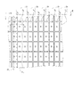
ここで、表示装置1には、複数の画素5が設定されている。複数の画素5は、表示領域7内で、図中のX方向及びY方向に配列しており、X方向を行方向とし、Y方向を列方向とするマトリクスMを構成している。表示装置1では、複数の画素5が、m(mは、1以上の整数)行、且つ2×n(nは、1以上の整数)列のマトリクスMを構成している。表示装置1は、複数の画素5から選択的に表示面3を介して表示装置1の外に光を射出することで、表示面3に画像を表示することができる。なお、表示領域7とは、画像が表示され得る領域である。図1では、構成をわかりやすく示すため、画素5が誇張されている。
Here, a plurality of
表示装置1は、図1中のA−A線における断面図である図2に示すように、素子基板11と、封止基板13とを有している。
素子基板11には、表示面3側すなわち封止基板13側に、複数の画素5のそれぞれに対応して、後述するスイッチング素子などが設けられている。
The
The
封止基板13は、素子基板11よりも表示面3側で素子基板11に対向した状態で設けられている。封止基板13には、表示装置1における表示面3の裏面に相当する面である底面15側すなわち素子基板11側に、後述する遮光膜などが設けられている。
素子基板11と封止基板13との間は、表示装置1の周縁よりも内側で表示領域7を囲むシール材17によって封止されている。
The sealing
The
ここで、表示装置1に設定されている複数の画素5は、それぞれ、表示面3から射出する光の色が、図3に示すように、赤系(R)、緑系(G)及び青系(B)のうちの1つに設定されている。つまり、マトリクスMを構成する複数の画素5は、Rの光を射出する画素5rと、Gの光を射出する画素5gと、Bの光を射出する画素5bとを含んでいる。
Here, in each of the plurality of
ここで、Rの色は、純粋な赤の色相に限定されず、橙等を含む。Gの色は、純粋な緑の色相に限定されず、青緑や黄緑を含む。Bの色は、純粋な青の色相に限定されず、青紫や青緑等を含む。他の観点から、Rの色を呈する光は、光の波長のピークが、可視光領域で570nm以上の範囲にある光であると定義され得る。また、Gの色を呈する光は、光の波長のピークが500nm〜565nmの範囲にある光であると定義され得る。Bの色を呈する光は、光の波長のピークが415nm〜495nmの範囲にある光であると定義され得る。 Here, the color of R is not limited to a pure red hue, and includes orange and the like. The color of G is not limited to a pure green hue, and includes blue-green and yellow-green. The color of B is not limited to a pure blue hue, and includes bluish purple and blue-green. From another viewpoint, light exhibiting the color of R can be defined as light having a light wavelength peak in a range of 570 nm or more in the visible light region. The light exhibiting the color G can be defined as light having a light wavelength peak in the range of 500 nm to 565 nm. Light exhibiting the color B can be defined as light having a light wavelength peak in the range of 415 nm to 495 nm.
マトリクスMでは、Y方向に沿って並ぶ複数の画素5が、1つの画素列21を構成している。また、X方向に沿って並ぶ複数の画素5が、1つの画素行23を構成している。1つの画素列21内の各画素5は、光の色がR、G及びBのうちの1つに設定されている。つまり、マトリクスMは、複数の画素5rがY方向に配列した画素列21rと、複数の画素5gがY方向に配列した画素列21gと、複数の画素5bがY方向に配列した画素列21bとを有している。そして、表示装置1では、画素列21r、画素列21g及び画素列21bが、この順で2列ずつX方向に沿って反復して並んでいる。
In the matrix M, a plurality of
また、表示装置1では、マトリクスMを構成する複数の画素5は、図4に示すように、複数の第1の画素51と、複数の第2の画素52とにわけられている。表示装置1は、複数の第1の画素51から選択的に表示面3を介して表示装置1の外に光を射出することで、表示面3に第1の画像を表示することができる。また、表示装置1は、複数の第2の画素52から選択的に表示面3を介して表示装置1の外に光を射出することで、表示面3に第2の画像を表示することができる。
In the
なお、第1の画像と第2の画像とは、互いに異なる画像であることと、互いに同じ画像であることとが問われない。また、以下においては、画素5という表記と、画素5r、5g及び5bという表記と、第1の画素51及び第2の画素52という表記とが、適宜、使いわけられる。また、第1の画素51及び第2の画素52のそれぞれに対してR、G及びBが識別される場合、第1の画素5r1、5g1及び5b1、並びに、第2の画素5r2、5g2及び5b2という表記が用いられる。
It should be noted that the first image and the second image may be different from each other or the same image. In the following, the
表示装置1では、第1の画素51と第2の画素52とが、X方向に交互に並んでいる。1つの画素列21は、複数の第1の画素51又は複数の第2の画素52によって構成されている。つまり、マトリクスMは、複数の第1の画素51がY方向に沿って配列した画素列211と、複数の第2の画素52がY方向に沿って配列した画素列212とを有している。なお、以下においては、画素列21という表記と、画素列21r、画素列21g及び画素列21bという表記と、画素列211及び画素列212という表記とが、適宜、使いわけられる。また、画素列211及び画素列212のそれぞれに対してR、G及びBが識別される場合、画素列21r1、21g1及び21b1、並びに、画素列21r2、21g2及び21b2という表記が用いられる。
In the
表示装置1では、マトリクスMを構成する複数の画素5は、X方向に隣り合う第1の画素51及び第2の画素52の2つの画素5ごとに、これらの2つの画素5を1組とする複数組の画素群25にわけられている。各画素群25での第1の画素51及び第2の画素52の並び順は、複数組の画素群25間で統一している。表示装置1では、第1の画素51と第2の画素52とが、図4で見て、X方向に左側から右側に向かってこの順で並んでいる。なお、第1の画素51及び第2の画素52の並び順は、複数組の画素群25間で統一していれば、いずれが左側でも右側でもよい。
In the
また、表示装置1では、各画素群25を構成する第1の画素51及び第2の画素52は、射出する光の色がR、G及びBのうちの1つに設定されている。つまり、第1の画素5r1及び第2の画素5r2が1組の画素群25を構成し、第1の画素5g1及び第2の画素5g2が1組の画素群25を構成し、第1の画素5b1及び第2の画素5b2が1組の画素群25を構成している。なお、以下において複数組の画素群25のそれぞれに対してR、G及びBが識別される場合、画素群25r、画素群25g及び画素群25bという表記が用いられる。
In the
マトリクスMにおいて、複数組の画素群25は、図5に示すように、X方向及びY方向のそれぞれの方向に沿って並んでいる。つまり、複数組の画素群25は、マトリクス状に配列している。
なお、表示装置1では、複数の画素5が、前述したように、m行且つ2×n列のマトリクスMを構成している。このため、複数組の画素群25は、m行、且つn列のマトリクスを構成している。
In the matrix M, a plurality of sets of
In the
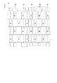
表示装置1は、回路構成を示す図である図6に示すように、画素5ごとに、選択トランジスタ27と、駆動トランジスタ29と、容量素子31と、画素電極33と、有機層35と、共通電極37とを有している。選択トランジスタ27及び駆動トランジスタ29は、それぞれ、TFT(Thin Film Transistor)素子で構成されており、スイッチング素子としての機能を有する。なお、表示装置1では、選択トランジスタ27としてNチャネル型のTFT素子が採用され、駆動トランジスタ29としてPチャネル型のTFT素子が採用されている。
As shown in FIG. 6, which is a diagram illustrating a circuit configuration, the
また、表示装置1は、m本の走査線GT1と、m本の走査線GT2と、n本のデータ線SI1と、n本のデータ線SI2と、m本の電源線PWとを有している。
なお、以下においてm本の走査線GT1のそれぞれが識別される場合に、走査線GT1(h)という表記が用いられる(hは、1〜mの整数)。同様に、m本の走査線GT2及びm本の電源線PWのそれぞれが識別される場合には、走査線GT2(h)という表記と、電源線PW(h)という表記とが用いられる。
また、n本のデータ線SI1及びn本のデータ線SI2のそれぞれが識別される場合には、データ線SI1(j)という表記と、データ線SI2(j)という表記とが用いられる(jは、1〜nの整数)。
Further, the
In the following description, when each of the m scanning lines GT 1 is identified, the notation of the scanning line GT 1 (h) is used (h is an integer of 1 to m). Similarly, when each of m scanning lines GT 2 and m power supply lines PW is identified, the notation of scanning line GT 2 (h) and the notation of power supply line PW (h) are used. .
When each of the n data lines SI 1 and the n data lines SI 2 is identified, the notation of the data line SI 1 (j) and the notation of the data line SI 2 (j) are used. (J is an integer from 1 to n).
m本の走査線GT1及び走査線GT2は、Y方向に互いに間隔をあけた状態で、X方向に沿って延びている。n本のデータ線SI1及びデータ線SI2は、X方向に互いに間隔をあけた状態で、Y方向に沿って延びている。m本の走査線GT1及びn本のデータ線SI1は、格子状に配線されている。各第1の画素51は、各走査線GT1と各データ線SI1との交差に対応して設定されている。
The m scanning lines GT 1 and the scanning lines GT 2 extend along the X direction while being spaced apart from each other in the Y direction. The n data lines SI 1 and data lines SI 2 extend along the Y direction with a space therebetween in the X direction. The m scanning lines GT 1 and the n data lines SI 1 are wired in a grid pattern. Each
同様に、m本の走査線GT2及びn本のデータ線SI2は、格子状に配線されている。各第2の画素52は、各走査線GT2と各データ線SI2との交差に対応して設定されている。
各走査線GT1及び各走査線GT2は、各画素行23(図3)に対応している。各画素行23において、走査線GT1は、図6に示すように、n個の第1の画素51に対応している。また、各画素行23において、走査線GT2は、n個の第2の画素52に対応している。
Similarly, the m scanning lines GT 2 and the n data lines SI 2 are wired in a grid pattern. Each
Each scanning line GT 1 and each scanning line GT 2 correspond to each pixel row 23 (FIG. 3). In each
各データ線SI1及び各データ線SI2は、各画素列21(図3)に対応している。各画素列21において、データ線SI1は、図6に示すように、m個の第1の画素51すなわち1つの画素列211(図4)に対応している。また、各画素列21において、データ線SI2は、m個の第2の画素52すなわち1つの画素列212(図4)に対応している。
m本の電源線PWは、図6に示すように、Y方向に互いに間隔をあけた状態で、X方向に沿って延びている。各電源線PWは、各画素行23(図3)に対応している。
Each data line SI 1 and each data line SI 2 correspond to each pixel column 21 (FIG. 3). In each
As shown in FIG. 6, the m power lines PW extend along the X direction in a state of being spaced apart from each other in the Y direction. Each power supply line PW corresponds to each pixel row 23 (FIG. 3).
図6に示す各選択トランジスタ27のゲート電極は、対応する各走査線GT1及びGT2に電気的につながっている。各選択トランジスタ27のソース電極は、対応する各データ線SI1及びSI2に電気的につながっている。選択トランジスタ27のドレイン電極は、駆動トランジスタ29のゲート電極及び容量素子31の一方の電極に電気的につながっている。
The gate electrode of each
容量素子31の他方の電極と、駆動トランジスタ29のソース電極は、それぞれ、対応する各電源線PWに電気的につながっている。
各駆動トランジスタ29のドレイン電極は、各画素電極33に電気的につながっている。各画素電極33と共通電極37とは、画素電極33を陽極とし、共通電極37を陰極とする一対の電極を構成している。
ここで、共通電極37は、マトリクスMを構成する複数の画素5間にわたって一連した状態で設けられており、複数の画素5間にわたって共通して機能する。
各画素電極33と共通電極37との間に介在する有機層35は、有機材料で構成されており、発光層を含んだ構成を有している。
The other electrode of the
The drain electrode of each
Here, the
The
選択トランジスタ27は、この選択トランジスタ27につながる走査線GT1及びGT2に走査信号が供給されるとON状態となる。このとき、この選択トランジスタ27につながるデータ線SI1及びSI2からデータ信号が供給され、駆動トランジスタ29がON状態になる。駆動トランジスタ29のゲート電位は、データ信号の電位が容量素子31に一定の期間だけ保持されることによって、一定の期間だけ保持される。これにより、駆動トランジスタ29のON状態が一定の期間だけ保持される。
The
駆動トランジスタ29のON状態が保持されているときに、駆動トランジスタ29のゲート電位に応じた電流が、電源線PWから画素電極33と有機層35を経て共通電極37に流れる。そして、有機層35に含まれる発光層が、有機層35を流れる電流量に応じた輝度で発光する。表示装置1は、有機層35に含まれる発光層が発光し、発光層からの光が封止基板13を介して表示面3から射出されるトップエミッション型の有機EL装置の1つである。
When the ON state of the driving
ここで、素子基板11及び封止基板13のそれぞれの構成について、詳細を説明する。
素子基板11は、図4中のC−C線における断面図である図7に示すように、第1基板41を有している。
第1基板41は、例えばガラスや石英などの光透過性を有する材料で構成されており、表示面3側に向けられた第1面42aと、底面15側に向けられた第2面42bとを有している。
Here, the details of the configurations of the
The
The
第1基板41の第1面42aには、ゲート絶縁膜43が設けられている。ゲート絶縁膜43の表示面3側には、絶縁膜45が設けられている。絶縁膜45の表示面3側には、絶縁膜47が設けられている。絶縁膜47の表示面3側には、絶縁膜49が設けられている。
また、第1基板41の第1面42aには、各画素5の駆動トランジスタ29に対応する第1半導体層51と、各画素5の選択トランジスタ27に対応する第2半導体層53とが設けられている。
A
A
第1半導体層51及び第2半導体層53は、平面図である図8に示すように、それぞれ各画素5に対応して設けられている。なお、図7に示す断面は、図8中のD−D線における断面に相当している。
第1半導体層51及び第2半導体層53は、Y方向に間隔をあけた状態でY方向に隣り合っている。
As shown in FIG. 8 which is a plan view, the
The
第1半導体層51は、ソース領域51aと、チャネル領域51bと、ドレイン領域51cと、電極部51dとを有している。ソース領域51aと、チャネル領域51bと、ドレイン領域51cとは、X方向に並んでいる。電極部51dとチャネル領域51b及びドレイン領域51cとは、Y方向に間隔をあけた状態でY方向に隣り合っている。また、電極部51dとソース領域51aとは、連接した状態でX方向に隣り合っている。
The
第2半導体層53は、ソース領域53aと、チャネル領域53bと、ドレイン領域53cとを有している。ソース領域53aと、チャネル領域53bと、ドレイン領域53cとは、X方向に並んでいる。
各画素群25における第1の画素51及び第2の画素52の間で、第1半導体層51同士及び第2半導体層53同士は、平面視での輪郭が回転対称の関係にある。
The
Between the
第1半導体層51及び第2半導体層53は、図7に示すように、ゲート絶縁膜43によって表示面3側から覆われている。なお、ゲート絶縁膜43の材料としては、例えば酸化シリコンなどの材料が採用され得る。
As shown in FIG. 7, the
ゲート絶縁膜43の表示面3側には、平面図である図9に示すように、第1半導体層51に重なる島状電極55と、走査線GT1及びGT2と、データ線SI1及びSI2とが設けられている。
島状電極55は、平面図である図10に示すように、ゲート電極部55aと、電極部55bとを有している。ゲート電極部55aと電極部55bとは、連接した状態でY方向に隣り合っている。
On the
As shown in FIG. 10 which is a plan view, the island-
ゲート電極部55aは、図8に示す第1半導体層51のチャネル領域51bに重なっている。電極部55bは、第1半導体層51の電極部51dに重なっている。電極部51d及び電極部55bは、容量素子31の一部を構成している。
走査線GT1及びGT2のそれぞれには、対応する画素5ごとに、各画素5に向かってY方向に分岐する2本のゲート電極部57が設けられている。各ゲート電極部57は、図8に示す第2半導体層53のチャネル領域53bに重なっている。
The
Each of the scanning lines GT 1 and GT 2 is provided with two
各画素5に対応する島状電極55と、この画素5に対応するデータ線SI1(SI2)とは、X方向に隣り合っている。表示装置1では、各画素群25における2つの島状電極55は、この画素群25における第1の画素51及び第2の画素52のそれぞれに対応するデータ線SI1とデータ線SI2とによってX方向に挟まれている。
また、各画素群25における2つの島状電極55は、この画素群25における第1の画素51及び第2の画素52のそれぞれに対応する走査線GT1と走査線GT2とによってY方向に挟まれている。
The island-shaped
Further, the two
島状電極55、走査線GT1及びGT2、並びにデータ線SI1及びSI2の材料としては、例えば、アルミニウム、銅、モリブデン、タングステン、クロムなどの金属や、これらを含む合金などが採用され得る。ゲート電極部55a(島状電極55)、ゲート電極部57(走査線GT1及びGT2)並びにデータ線SI1及びSI2は、図7に示すように、絶縁膜45によって表示面3側から覆われている。
絶縁膜45には、平面図である図11に示すように、各画素5に対応してコンタクトホールCH1,CH2,CH3,CH4,CH5,CH6及びCH7が設けられている。
各コンタクトホールCH1は、各データ線SI1及びSI2に対応して、各データ線SI1及びSI2に重なる部位に設けられている。各コンタクトホールCH1は、第2半導体層53のソース領域53aとはX方向に対峙する部位に設けられている。各コンタクトホールCH1は、対応する各データ線SI1及びSI2に及んでいる。
As shown in FIG. 11 which is a plan view, the insulating
Each contact hole CH1 is provided in a portion overlapping each data line SI 1 and SI 2 corresponding to each data line SI 1 and SI 2 . Each contact hole CH1 is provided at a portion facing the
各コンタクトホールCH2は、各ソース領域53aに対応して、各ソース領域53aに重なる部位に設けられている。各コンタクトホールCH2は、各コンタクトホールCH1とはX方向に対峙する部位に設けられている。各コンタクトホールCH2は、第2半導体層53のソース領域53aに及んでいる。
Each contact hole CH2 is provided in a portion corresponding to each
各コンタクトホールCH3は、各ドレイン領域53cに対応して、各ドレイン領域53cに重なる部位に設けられている。各コンタクトホールCH3は、第2半導体層53のドレイン領域53cに及んでいる。
各コンタクトホールCH4は、各電極部55bに対応して、各電極部55bに重なる部位に設けられている。各コンタクトホールCH4は、各コンタクトホールCH3とはY方向に対峙する部位に設けられている。各コンタクトホールCH4は、各電極部55bに及んでいる。
Each contact hole CH3 is provided in a portion corresponding to each
Each contact hole CH4 is provided at a portion corresponding to each
コンタクトホールCH5は、各第1半導体層51の各ドレイン領域51cに対応して、各ドレイン領域51cに重なる部位に2つずつ設けられている。各コンタクトホールCH5は、第1半導体層51のドレイン領域51cに及んでいる。
各コンタクトホールCH6は、各データ線SI1及びSI2に対応して、各データ線SI1及びSI2に重なる部位に設けられている。各コンタクトホールCH6は、X方向にソース領域51aを挟んでゲート電極部55aとは対峙する部位に設けられている。各コンタクトホールCH6は、対応する各データ線SI1及びSI2に及んでいる。
Two contact holes CH5 are provided corresponding to each
Each contact hole CH6 is provided in a portion overlapping each data line SI 1 and SI 2 corresponding to each data line SI 1 and SI 2 . Each contact hole CH6 is provided at a portion facing the
コンタクトホールCH7は、各ソース領域51aに対応して、各ソース領域51aに重なる部位に2つずつ設けられている。各コンタクトホールCH7は、平面視で、各画素5に対応する各データ線SI1及びSI2と島状電極55の電極部55bとの間で、電極部55bとはX方向に対峙する部位に設けられている。各コンタクトホールCH7は、第1半導体層51のソース領域51aに及んでいる。
Two contact holes CH7 are provided corresponding to each
コンタクトホールCH1〜CH7が設けられた絶縁膜45の表示面3側には、平面図である図12に示すように、電源線PWと、ドレイン電極59と、中継電極61と、中継電極63とが設けられている。
各電源線PWは、各画素行23(図3)をX方向にまたぐ長さにわたって一連した状態で設けられている。各電源線PWは、Y方向の幅寸法が、図12に示すように、Y方向に並ぶ2つのコンタクトホールCH7をまたぐ長さに設定されている。各電源線PWは、各画素行23における複数のコンタクトホールCH7を覆っている。
On the
Each power supply line PW is provided in a state in which each pixel row 23 (FIG. 3) is arranged in a series extending over a length extending in the X direction. Each power supply line PW is set to have a width across the two contact holes CH7 aligned in the Y direction as shown in FIG. Each power supply line PW covers a plurality of contact holes CH7 in each
各画素5において、電源線PWは、平面視で選択トランジスタ27と駆動トランジスタ29との間に位置している。換言すれば、選択トランジスタ27と駆動トランジスタ29とは、電源線PWを挟んでY方向に対峙している。また、選択トランジスタ27のソース領域53a、チャネル領域53b(図8)及びドレイン領域53cは、平面視で電源線PWの外側に位置している。駆動トランジスタ29のソース領域51aの一部と、チャネル領域51b(図8)と、ドレイン領域51cとは、平面視で電源線PWの外側に位置している。
In each
また、1組の画素群25における第1の画素51及び第2の画素52間で、一方の選択トランジスタ27と、他方の駆動トランジスタ29とは、図12に示すように、X方向に隣り合っている。1組の画素群25における第1の画素51及び第2の画素52間で、選択トランジスタ27同士は、Y方向に電源線PWを挟んで互いに反対側に位置している。同様に、1組の画素群25における第1の画素51及び第2の画素52間で、駆動トランジスタ29同士は、Y方向に電源線PWを挟んで互いに反対側に位置している。
Further, between the pair of
各電源線PWは、図12中のE−E線における断面図である図13に示すように、コンタクトホールCH7を介して第1半導体層51のソース領域51aに達している。なお、表示装置1では、各電源線PWからコンタクトホールCH7を介してソース領域51aに達している部位が、ソース電極部65と呼ばれる。
前述したように、各コンタクトホールCH7は、平面視で、各画素5に対応する各データ線SI1及びSI2と島状電極55の電極部55bとの間に設けられている。このため、各ソース電極部65は、平面視で、各画素5に対応する各データ線SI1及びSI2と島状電極55の電極部55bとの間に位置している。
Each power supply line PW reaches the
As described above, each contact hole CH7 is provided between each data line SI 1 and SI 2 corresponding to each
ここで、平面視で電源線PWと島状電極55の電極部55bと第1半導体層51の電極部51dとが重なる領域に、容量素子31が形成される。このため、容量素子31は、第1基板41及び電源線PWの間に設けられているとみなされ得る。電極部55b、電極部51d及び電源線PWは、容量素子31の一部を構成している。
Here, the
ドレイン電極59は、図12に示すように、各画素5に対応して設けられており、コンタクトホールCH5を覆っている。各ドレイン電極59は、図7中のF部の拡大図である図14に示すように、コンタクトホールCH5を介して第1半導体層51のドレイン領域51cに達している。表示装置1では、ドレイン電極59からコンタクトホールCH5を介してドレイン領域51cに達している部位が、接続部67と呼ばれる。
As shown in FIG. 12, the
中継電極61は、図12に示すように、各画素5に対応して設けられている。各中継電極61は、Y方向に隣り合う2つの画素5間で、一方の画素5に対応するコンタクトホールCH1と、他方の画素5に対応するコンタクトホールCH6とにまたがっている。また、各画素5において、各中継電極61は、コンタクトホールCH1とコンタクトホールCH2との間にまたがっている。
The
各中継電極61は、Y方向に隣り合う2つの画素5のうちの一方に対応するコンタクトホールCH1及びCH2と、2つの画素5のうちの他方に対応するコンタクトホールCH6とを覆っている。これにより、Y方向に隣り合う2つのデータ線SI1同士が、中継電極61を介して電気的に接続される。また、Y方向に隣り合う2つのデータ線SI2同士も、中継電極61を介して電気的に接続される。
さらに、データ線SI1と、これに対応する第2半導体層53のソース領域53aとが、中継電極61を介して電気的に接続される。また、データ線SI2と、これに対応する第2半導体層53のソース領域53aとが、中継電極61を介して電気的に接続される。
Each
Further, the data line SI 1 and the
中継電極63は、各画素5に対応して設けられており、各画素5に対応するコンタクトホールCH3とコンタクトホールCH4との間にまたがっている。各中継電極63は、電源線PWの輪郭よりも外側で、これらのコンタクトホールCH3及びCH4を覆っている。これにより、各画素5において、第2半導体層53のドレイン領域53cと島状電極55の電極部55bとが、電源線PWの輪郭よりも外側で、中継電極63を介して電気的に接続される。
The
電源線PW、ドレイン電極59、中継電極61及び中継電極63の材料としては、例えば、アルミニウム、銅、モリブデン、タングステン、クロムなどの金属や、これらを含む合金などが採用され得る。ドレイン電極59、中継電極61及び中継電極63は、図7に示すように、絶縁膜47によって表示面3側から覆われている。なお、電源線PWも、絶縁膜47によって表示面3側から覆われている。
絶縁膜47は、絶縁膜49によって表示面3側から覆われている。
As a material for the power supply line PW, the
The insulating
絶縁膜47及び絶縁膜49には、コンタクトホールCH8が設けられている。
各コンタクトホールCH8は、図12に示すように、各画素5に対応して設けられている。各コンタクトホールCH8は、ドレイン電極59に重なる領域に設けられており、ドレイン電極59に及んでいる。
なお、各ドレイン電極59は、X方向にゲート電極部55aとは反対側に延長されている。そして、各コンタクトホールCH8は、平面視でドレイン電極59の延長された部位に重なっている。これにより、平面視でコンタクトホールCH5とコンタクトホールCH8とが重なっていない。ここで、コンタクトホールCH5とコンタクトホールCH8とは重なっていてもよい。
The insulating
Each contact hole CH8 is provided corresponding to each
Each
コンタクトホールCH8が設けられた絶縁膜49の表示面3側には、図7に示すように、画素5ごとに画素電極33が設けられている。
各画素電極33は、平面図である図15に示すように、Y方向には走査線GT1及び走査線GT2にまたがっており、X方向にはコンタクトホールCH8と、各画素5に対応するデータ線SI1又はデータ線SI2とにまたがっている。各画素電極33は、コンタクトホールCH8を覆っている。
As shown in FIG. 7, a
As shown in FIG. 15 which is a plan view, each
なお、表示装置1では、各画素電極33からコンタクトホールCH8を介してドレイン電極59に達している部位が、図14に示すように、接続部69と呼ばれる。
画素電極33の材料としては、銀、アルミニウム、銅などの光反射性を有する金属や、これらを含む合金などが採用され得る。画素電極33を陽極として機能させる場合には、銀、白金などの仕事関数が比較的高い材料を用いることが好ましい。また、画素電極33としてITO(Indium Tin Oxide)やインジウム亜鉛酸化物(Indium Zinc Oxide)などを用い、光反射性を有する部材を画素電極33と第1基板41との間に設けた構成も採用され得る。
また、絶縁膜47及び49の材料としては、例えば、酸化シリコン、窒化シリコン、アクリル系の樹脂などの材料が採用され得る。
In the
As a material of the
Further, as the material of the insulating
隣り合う画素電極33同士の間には、図7に示すように、各画素5の有効領域を区画するバンク71が領域72にわたって設けられている。バンク71は、隣り合う画素電極33同士間で絶縁膜49に及んでいる。バンク71は、例えば、カーボンブラックやクロムなどの光吸収性が高い材料を含有するアクリル系の樹脂やポリイミドなどの樹脂で構成されており、平面図である図16に示すように、格子状に設けられている。
Between the
バンク71は、表示領域7にわたって設けられている。このため、表示領域7は、バンク71によって複数の画素5の有効領域が区画されている。なお、各画素電極33は、図16に示すように、周縁部がバンク71に平面視で重なっている。
ここで、バンク71には、X方向に隣り合う画素群25同士間の部位であるバンク71aと、1組の画素群25内の第1の画素51及び第2の画素52間の部位であるバンク71bとが含まれている。バンク71bのX方向における幅寸法は、バンク71aのX方向における幅寸法よりも長く設定されている。
The
Here, the
そして、各画素5において、画素電極33の接続部69及びコンタクトホールCH8は、図14及び図16に示すように、平面視でバンク71bに重なっている。つまり、接続部69及びコンタクトホールCH8は、平面視でバンク71bに隠されている。
In each
画素電極33の表示面3側には、図7に示すように、バンク71に囲まれた領域内に、有機層35が設けられている。
有機層35は、各画素5に対応して設けられており、正孔注入層73と、正孔輸送層75と、発光層77とを有している。
正孔注入層73は、有機材料で構成されており、平面視でバンク71によって囲まれた領域内で、画素電極33の表示面3側に設けられている。正孔注入層73は、液状の有機材料を塗布することによって設けられ得る。
正孔注入層73の材料としては、3,4−ポリエチレンジオキシチオフェン(PEDOT)等のポリチオフェン誘導体と、ポリスチレンスルホン酸(PSS)等との混合物が採用され得る。正孔注入層73の材料としては、ポリスチレン、ポリピロール、ポリアニリン、ポリアセチレンやこれらの誘導体なども採用され得る。
On the
The
The
As a material of the
正孔輸送層75は、有機材料で構成されており、平面視でバンク71によって囲まれた領域内で、正孔注入層73の表示面3側に設けられている。正孔輸送層75は、液状の有機材料を塗布することによって設けられ得る。
正孔輸送層75の材料としては、例えば、下記化合物1として示されるTFBなどのトリフェニルアミン系ポリマーを含んだ構成が採用され得る。
The
As a material of the

発光層77は、有機材料で構成されており、平面視でバンク71によって囲まれた領域内で、正孔輸送層75の表示面3側に設けられている。発光層77は、液状の有機材料を塗布することによって設けられ得る。
Rの画素5rに対応する発光層77の材料としては、例えば、下記化合物2として示されるCN−PPVが採用され得る。
The
As a material of the
Gの画素5gに対応する発光層77の材料としては、例えば、下記化合物3として示されるF8BTと、上記化合物1として示されるTFBとを、1:1で混合したものが採用され得る。
As a material of the
Bの画素5bに対応する発光層77の材料としては、例えば、下記化合物4として示されるF8(ポリジオクチルフルオレン)が採用され得る。
As a material of the
有機層35の表示面3側には、図7に示すように、共通電極37が設けられている。共通電極37は、例えば、ITOやインジウム亜鉛酸化物等の光透過性を有する材料や、マグネシウム銀等を薄膜化して光透過性を付与したものなどで構成され、有機層35及びバンク71を表示面3側から複数の画素5間にわたって覆っている。
なお、表示装置1では、各画素5において発光する領域は、平面視で、バンク71によって囲まれた領域内で画素電極33と有機層35と共通電極37とが重なる領域であると定義され得る。
As shown in FIG. 7, a
In the
共通電極37の表示面3側には、補助配線39が設けられている。補助配線39は、共通電極37よりも表示面3側でバンク71bに平面視で重なる領域に設けられている。補助配線39としては、例えば、アルミニウム、銅、金、銀、モリブデン、タングステン、クロムなどの金属や、これらを含む合金などが採用され得る。
この補助配線39は、共通電極37に導通しており、共通電極37の電気伝導を補助する機能を有している。
An
The
封止基板13は、第2基板81を有している。第2基板81は、例えばガラスや石英などの光透過性を有する材料で構成されており、表示面3側に向けられた外向面82aと、底面15側に向けられた対向面82bとを有している。
第2基板81の対向面82bには、遮光膜83が設けられている。遮光膜83は、例えば、カーボンブラックなどを含有する樹脂や、クロムなどの光吸収性が高い材料で構成され得る。遮光膜83は、マトリクスMを構成する複数の画素5間にわたって設けられている。つまり、遮光膜83は、マトリクスMを構成する複数の画素5に平面視で重なる領域に設けられている。
The sealing
A
遮光膜83には、各画素群25を構成する第1の画素51及び第2の画素52に平面視で重なる開口部85が設けられている。
各開口部85は、遮光膜83と画素群25との平面図である図17に示すように、各画素群25に対応して設けられている。まお、この図17では、構成をわかりやすく示すため、遮光膜83にハッチングが施されている。
The
Each
また、第2基板81の対向面82bには、図7に示すように、開口部85内の領域を底面15側から覆うカラーフィルタ87が設けられている。カラーフィルタ87は、開口部85ごとに設けられている。
ここで、カラーフィルタ87は、入射された光のうち所定の波長域の光を透過させることができる。カラーフィルタ87は、画素群25r、画素群25g及び画素群25bごとに異なる色に着色された樹脂などで構成されている。
Further, as shown in FIG. 7, a
Here, the
画素群25rに対応するカラーフィルタ87は、Rの光を透過させることができる。画素群25gに対応するカラーフィルタ87はGの光を透過させ、画素群25bに対応するカラーフィルタ87はBの光を透過させることができる。なお、以下において、各カラーフィルタ87に対してR、G及びBが識別される場合に、カラーフィルタ87r、87g及び87bという表記が用いられる。
The
ここで、表示装置1では、画素5rの発光層77がRの光を射出する。画素5rの発光層77から射出されたRの光は、カラーフィルタ87rを透過することによってRの色純度が高められる。また、画素5gの発光層77から射出されたGの光は、カラーフィルタ87gを透過することによってGの色純度が高められ、画素5bの発光層77から射出されたBの光は、カラーフィルタ87bを透過することによってBの色純度が高められる。
Here, in the
遮光膜83及びカラーフィルタ87の底面15側には、オーバーコート層89が設けられている。オーバーコート層89は、光透過性を有する樹脂などで構成されており、遮光膜83及びカラーフィルタ87を底面15側から覆っている。
An
オーバーコート層89の底面15側には、樹脂層93が設けられている。樹脂層93は、例えばアクリル系の樹脂やエポキシ系の樹脂などの光透過性を有する材料で構成されており、各画素5に対応してプリズム部95a及び95bが形成されている。表示装置1では、プリズム部95aが第1の画素51に対応し、プリズム部95bが第2の画素52に対応している。
A
上記の構成を有する封止基板13及び素子基板11は、樹脂層93のプリズム部95a及び95b側と共通電極37側とが対向した状態で、樹脂層93と共通電極37とが接着剤97を介して接合されている。
表示装置1では、図2に示すシール材17は、図7に示す第1基板41の第1面42aと、第2基板81の対向面82bとによって挟持されている。つまり、表示装置1では、接着剤97が、第1基板41及び第2基板81並びにシール材17によって封止されている。なお、シール材17は、樹脂層93及び共通電極37の間に設けられていてもよい。この場合、接着剤97は、素子基板11及び封止基板13並びにシール材17によって封止されているとみなされ得る。
In the sealing
In the
なお、接着剤97は、樹脂層93のプリズム部95a及び95b内に及んでいる。また、接着剤97の材料としては、光透過性を有し、且つ屈折率が樹脂層93の屈折率とは異なるものが採用され得る。これにより、各画素5の発光層77から、対応するプリズム部95a及び95bに至る光を、プリズム部95a及び95bのそれぞれで屈折させることができる。
表示装置1では、樹脂層93の屈折率が、接着剤97の屈折率よりも高く設定されている。そして、各プリズム部95a及び95bは、対応する各画素5の発光層77からの光を開口部85側へ屈折させるように形状が設定されている。
Note that the adhesive 97 extends into the
In the
上記の構成を有する表示装置1では、発光層77を画素5ごとに発光させることにより、表示が制御される。発光層77の発光状態は、各有機層35を流れる電流を各駆動トランジスタ29で制御することによって画素5ごとに変化し得る。
In the
各走査線GT1(h)には、図6に示すように、制御信号CS1(h)が供給される。同様に、各走査線GT2(h)には、制御信号CS2(h)が供給される。制御信号CS1(h)と制御信号CS2(h)とは、交互に供給される。つまり、走査線GT1(1)に、制御信号CS1(1)が供給された後に、走査線GT2(1)に制御信号CS2(1)が供給される。 As shown in FIG. 6, a control signal CS 1 (h) is supplied to each scanning line GT 1 (h). Similarly, the control signal CS 2 (h) is supplied to each scanning line GT 2 (h). The control signal CS 1 (h) and the control signal CS 2 (h) are supplied alternately. That is, the scan line GT 1 (1), after the control signal CS 1 (1) is supplied, the scan line GT 2 (1) to the control signal CS 2 (1) is supplied.
各データ線SI1(j)には、画像信号DS1(j)がパラレル信号として供給される。同様に、各データ線SI2(j)には、画像信号DS2(j)がパラレル信号として供給される。画像信号DS1(j)と画像信号DS2(j)とは、交互に供給される。つまり、データ線SI1(1)〜SI1(n)に画像信号DS1(1)〜DS1(n)が供給された後に、データ線SI2(1)〜SI2(n)に画像信号DS2(1)〜DS2(n)が供給される。 The image signal DS 1 (j) is supplied as a parallel signal to each data line SI 1 (j). Similarly, the image signal DS 2 (j) is supplied as a parallel signal to each data line SI 2 (j). The image signal DS 1 (j) and the image signal DS 2 (j) are supplied alternately. That is, the data line SI 1 (1) ~SI after the image signal DS 1 (1) ~DS 1 ( n) is supplied to the 1 (n), the image data line SI 2 (1) ~SI 2 ( n) signal DS 2 (1) ~DS 2 ( n) are supplied.
制御信号CS1(h)及び制御信号CS2(h)は、図18に示すように、それぞれ、1フレーム期間内に1回だけ、1フレーム期間よりも短い期間t1にわたってHiレベルの選択電位に維持される。あるタイミングで選択電位となり得るのは、制御信号CS1(h)及び制御信号CS2(h)のうちの1つだけである。 As shown in FIG. 18, the control signal CS 1 (h) and the control signal CS 2 (h) are set to the Hi level selection potential only once in one frame period over a period t1 shorter than one frame period. Maintained. Only one of the control signal CS 1 (h) and the control signal CS 2 (h) can become the selection potential at a certain timing.
走査線GT1(h)が選択電位となると、この走査線GT1(h)に対応する複数の第1の画素51の選択トランジスタ27がON状態となる。このとき、データ線SI1(1)〜SI1(n)に供給された画像信号DS1(1)〜DS1(n)が、選択トランジスタ27を介して、駆動トランジスタ29のゲート電極部55a及び電極部55b(図12)に供給される。つまり、第1の画素51において、ゲート電極部55a及び電極部55bは、画像信号DS1(j)の電位に応じた電位となる。
When the scanning line GT 1 (h) is selected potential, the plurality of
同様に、走査線GT2(h)が選択電位となると、この走査線GT2(h)に対応する複数の第2の画素52の選択トランジスタ27がON状態となる。このとき、データ線SI2(1)〜SI2(n)に供給された画像信号DS2(1)〜DS2(n)が、選択トランジスタ27を介して、駆動トランジスタ29のゲート電極部55a及び電極部55b(図12)に供給される。つまり、第2の画素52において、ゲート電極部55a及び電極部55bは、画像信号DS2(j)の電位に応じた電位となる。
Similarly, when the scanning line GT 2 (h) is selected potential, the plurality of
このとき、駆動トランジスタ29のゲート電極部55aの電位に応じた電流が、電源線PW(h)からソース領域51a及びチャネル領域51bを介してドレイン領域51cに流れる。
そして、電源線PW(h)からの電流は、ドレイン電極59及び画素電極33を経て有機層35(図7)を流れる。
他方で、電極部55b及び電源線PW(h)の間(図13)と、電極部55b及び電極部51dの間とには、電荷が蓄積されるので、駆動トランジスタ29のゲート電極部55aの電位は、一定期間だけ保持される。この結果、ゲート電極部55aの電位が保持されている期間において、電流が有機層35を流れつづける。
At this time, a current corresponding to the potential of the
Then, the current from the power supply line PW (h) flows through the organic layer 35 (FIG. 7) through the
On the other hand, since charges are accumulated between the
このように、表示装置1では、画像信号DS1(j)や画像信号DS2(j)の電位に応じた電流が有機層35を流れるので、画素5ごとに発光層77からの光を画像信号DS1(j)の電位に応じた輝度に制御することができる。これにより、表示装置1では、階調表示が行われ得る。
また、表示装置1では、第1の画素51及び第2の画素52ごとに、画像信号DS1(j)と画像信号DS2(j)とを異なるタイミングで供給することができる。このため、第1の画像に対応する画像信号DS1(j)と、第2の画像に対応する画像信号DS2(j)とをわけて処理することができる。この結果、第1の画像に対応する画像信号DS1(j)と、第2の画像に対応する画像信号DS2(j)とを合成して同じタイミングで供給するための処理を省略することができる。
As described above, in the
In the
ここで、表示装置1は、前述したように、画素群25ごとに開口部85が設けられた遮光膜83を有している。各第1の画素51の発光層77からの光は、開口部85を介して表示面3に向けて射出される。
このとき、各第1の画素51から表示面3側に向けて射出された光111aは、複数組の画素群25及び遮光膜83を模式的に示す断面図である図19に示すように、各開口部85を介して第1の範囲113に及ぶ。
また、各第2の画素52から表示面3側に向けて射出された光111bは、各開口部85を介して第2の範囲115に及ぶ。なお、図19に示す断面は、図1中のA−A線における断面に相当している。
Here, as described above, the
At this time, the light 111a emitted toward the
Further, the light 111b emitted toward the
第1の範囲113からは、開口部85を介して第1の画素51からの光111aが視認され得る。第2の範囲115からは、開口部85を介して第2の画素52からの光111bが視認され得る。第1の範囲113内に視点があれば、複数の第1の画素51からの光111aによって形成される第1の画像が視認され得る。第2の範囲115内に視点があれば、複数の第2の画素52からの光111bによって形成される第2の画像が視認され得る。つまり、表示装置1では、第1の画像を第1の範囲113に表示し、第2の画像を、第1の範囲113とは異なる第2の範囲115に表示する所謂指向性表示を行うことができる。
From the
第1の範囲113及び第2の範囲115は、互いに重複する範囲117を有している。この範囲117からは、第1の画像と第2の画像とが重畳した状態で視認される。第1の範囲113から範囲117を除いた範囲119a(以下、適視範囲119aと呼ぶ)からは、第1の画像だけが視認され得る。また、第2の範囲115から範囲117を除いた範囲119b(以下、適視範囲119bと呼ぶ)からは、第2の画像だけが視認され得る。
The
表示装置1は、複数の第1の画素51から射出された光111aが第1の範囲113の両端のそれぞれにおいて交差し、複数の第2の画素52から射出された光111bが第2の範囲115の両端のそれぞれにおいて交差するように構成されている。これは、X方向に隣り合う開口部85同士間の間隔Paを、X方向に隣り合う画素群25同士間の間隔Pbよりも短く設定することによって実現され得る。
これにより、適視範囲119a内にある任意の視点から視認される光の量を、複数の第1の画素51間で同等にすることができる。同様に、適視範囲119b内にある任意の視点から視認される光の量を、複数の第2の画素52間で同等にすることができる。
Thus, the amounts of lights viewed from any viewpoint within
表示装置1において、遮光膜83が遮光層に対応し、画素電極33が第1電極に対応し、共通電極37が第2電極に対応し、駆動トランジスタ29がスイッチング素子に対応し、プリズム部95a及び95bがプリズムとしての光学素子に対応し、画素5rが赤系画素に対応し、画素5gが緑系画素に対応し、画素5bが青系画素に対応し、カラーフィルタ87rが赤系フィルタに対応し、カラーフィルタ87gが緑系フィルタに対応し、カラーフィルタ87bが青系フィルタに対応している。
In the
表示装置1では、遮光膜83が第2基板81に設けられている。つまり、遮光膜83は、第1基板41と第2基板81との間に介在している。このため、遮光膜83が素子基板11及び封止基板13の外側に配置される場合に比較して、複数の画素5と遮光膜83との間の距離を短縮することができる。従って、指向性表示における適視範囲119aや適視範囲119bを拡大しやすくすることができる。
In the
また、表示装置1では、電源線PWがX方向に延びている。このため、例えば、X方向に隣り合う画素5同士間に沿ってY方向に電源線PWが延びる場合に比較して、X方向における画素5同士間の間隔を縮めやすくすることができる。これにより、X方向における画素密度を高めやすくすることができる。この結果、指向性表示における高精細化を図りやすくすることができる。
In the
また、表示装置1では、発光層77からの光が封止基板13を介して表示面3から射出されるトップエミッション型の有機EL装置が採用されている。
ここで、発光層77からの光が素子基板11の第1基板41を経て射出されるボトムエミッション型を採用した場合、発光層77と遮光膜83との間に第1基板41が介在することになる。このため、ボトムエミッション型では、発光層77と遮光膜83との間の距離を短縮することが困難になる。
ところが、表示装置1では、トップエミッション型が採用されているので、発光層77と遮光膜83との間の距離を短縮しやすくすることができる。
In the
Here, when a bottom emission type in which light from the
However, since the
また、表示装置1では、選択トランジスタ27や駆動トランジスタ29が発光層77よりも底面15側に設けられている。他方で、発光層77からの光は、封止基板13を介して表示面3から射出される。つまり、選択トランジスタ27や駆動トランジスタ29は、発光層77から表示面3側に向かう光の進行を妨げない。従って、発光層77からの光の利用効率を高めやすくすることができる。他方で、選択トランジスタ27や駆動トランジスタ29などの平面視での配置位置の自由度を高めやすくすることができる。
In the
また、表示装置1では、発光層77と遮光膜83との間に樹脂層93が介在している。樹脂層93では、ガラスや石英などの脆性材料に比較して厚みを容易に調整することができる。このため、表示装置1では、樹脂層93の厚みを調整することで、適視範囲119aや適視範囲119bを調整しやすくすることができる。
In the
また、表示装置1では、樹脂層93にプリズム部95a及び95bが設けられている。このため、発光層77からの光を各開口部85へ導きやすくすることができる。これにより、光の利用効率を一層高めやすくすることができる。
In the
また、表示装置1では、複数の発光層77は、画素5ごとにRの光を発する発光層77と、Gの光を発する発光層77と、Bの光を発する発光層77とにわけられている。このため、指向性表示においてカラー表示を行うことができる。
In the
また、表示装置1では、開口部85ごとにカラーフィルタ87が設けられている。各開口部85は、各画素群25に対応している。このため、各画素群25を構成する第1の画素51と第2の画素52とに1つのカラーフィルタ87を共用させることができる。
また、各カラーフィルタ87が各開口部85内に設けられているので、表示装置1の厚みを低減しやすくすることができる。
In the
In addition, since each
また、表示装置1では、容量素子31が第1基板41及び電源線PWの間に設けられており、且つ平面視で電源線PWに重なっているので、各画素5の領域を縮小しやすくすることができる。これにより、画素密度を一層高めやすくすることができ、指向性表示における高精細化を一層図りやすくすることができる。
Further, in the
また、表示装置1では、各画素5において選択トランジスタ27及び駆動トランジスタ29が、平面視でY方向に電源線PWを挟んで対峙する位置に設けられている。このため、選択トランジスタ27及び駆動トランジスタ29の間に容量素子31を設けやすくすることができる。この結果、各画素5の領域を縮小しやすくすることができる。
In the
また、表示装置1では、駆動トランジスタ29のソース領域51aと、チャネル領域51bと、ドレイン領域51cとが、X方向に並んでいる。そして、選択トランジスタ27のソース領域53aと、チャネル領域53bと、ドレイン領域53cとが、X方向に並んでいる。このため、選択トランジスタ27及び駆動トランジスタ29の間の領域を広げやすくすることができる。これにより、選択トランジスタ27及び駆動トランジスタ29の間に容量素子31を一層設けやすくすることができる。
Further, in the
また、表示装置1では、駆動トランジスタ29において、島状電極55がゲート電極部55aと電極部55bとを有し、第1半導体層51が電極部51dを有している。電極部55bと電極部51dとは、互いに対向しているとともに、平面視で電源線PWに重なっている。そして、電極部55bが選択トランジスタ27のドレイン領域53cに電気的につながっており、電極部51dが電源線PWに電気的につながっている。このため、電極部55b、電極部51d及び電源線PWに、容量素子31の一部を構成させることができる。
In the
他方で、島状電極55のゲート電極部55aと、第1半導体層51のソース領域51a、チャネル領域51b及びドレイン領域51cとは、駆動トランジスタ29を構成している。つまり、表示装置1では、駆動トランジスタ29と容量素子31とを共用することができる。この結果、各画素5の領域を一層縮小しやすくすることができ、指向性表示における高精細化を一層図りやすくすることができる。
On the other hand, the
また、表示装置1では、第1半導体層51のドレイン領域51cが、平面視で電源線PWの外側に設けられている。そして、第1半導体層51のドレイン領域51cと各画素電極33とが、平面視で電源線PWの外側で電気的につながっている。このため、電源線PWに阻害されることなく、各駆動トランジスタ29と各画素電極33とを電気的につなげることができる。
In the
また、表示装置1では、1組の画素群25における第1の画素51及び第2の画素52間で、第1半導体層51のドレイン領域51c同士が、平面視で電源線PWを挟んで互いに反対側に位置している。このため、これらの第1の画素51及び第2の画素52間で、第1半導体層51のドレイン領域51c同士を遠ざけやすくすることができる。従って、これらの第1の画素51及び第2の画素52間で、コンタクトホールCH8同士を遠ざけやすくすることができる。これにより、これらの第1の画素51及び第2の画素52において、各コンタクトホールCH8の平面視での領域を拡大しやすくすることができる。この結果、各接続部69の平面視での領域を拡大しやすくすることができ、各接続部69における電気伝導を向上させやすくすることができる。
In the
また、表示装置1では、走査線GT1が第1の画素51に対応しており、走査線GT2が第2の画素52に対応して設けられている。このため、複数の選択トランジスタ27を、第1の画素51及び第2の画素52ごとに異なるタイミングでON状態にすることができる。これにより、第1の画素51及び第2の画素52ごとに、画像信号DS1(j)と画像信号DS2(j)とを異なるタイミングで供給することができる。この結果、第1の画像に対応する画像信号DS1(j)と、第2の画像に対応する画像信号DS2(j)とをわけて処理することができる。
In the
また、表示装置1では、1組の画素群25における第1の画素51及び第2の画素52において、各選択トランジスタ27及び各駆動トランジスタ29が、これらの第1の画素51及び第2の画素52に対応するデータ線SI1及びデータ線SI2の間に位置している。このため、これらの第1の画素51及び第2の画素52のX方向における間隔を縮めやすくすることができる。
In the
また、表示装置1では、電源線PWが、X方向に隣り合う画素群25同士の間をまたいでいる。X方向に隣り合う画素群25同士の間には、2つのデータ線SI1及びSI2がY方向に延びている。電源線PWは、これら2つのデータ線SI1及びSI2をX方向にまたいでいる。
ここで、2つのデータ線SI1及びSI2間には、寄生容量が形成されやすい。ところが、表示装置1では、電源線PWがこれら2つのデータ線SI1及びSI2をまたいでいるので、電源線PWとデータ線SI1との間、及び電源線PWとデータ線SI2との間のそれぞれの間に容量が形成されやすい。このため、これらの2つのデータ線SI1及びSI2間の電気的な干渉を軽減しやすくすることができ、表示品位の向上が図られる。
In the
Here, a parasitic capacitance is easily formed between the two data lines SI 1 and SI 2 . However, in the
また、表示装置1では、コンタクトホールCH7及びソース電極部65が、平面視で各画素5に対応する各データ線SI1及びSI2と島状電極55の電極部55bとの間に設けられている。このため、容量素子31と各データ線SI1及びSI2との間の電気的な干渉を軽減しやすくすることができ、表示品位の向上が図られる。
In the
また、表示装置1では、画素電極33の接続部69及びコンタクトホールCH8が、平面視でバンク71bに重なっている。このため、平面視で、接続部69及びコンタクトホールCH8をバンク71bで隠しやすくすることができる。
Further, in the
また、表示装置1では、補助配線39とバンク71とが平面視で重なっている。このため、補助配線39は、各発光層77から表示面3側に向かう光の進行を妨げない。従って、補助配線39には、遮光性を有する材料を採用することができる。また、補助配線39の厚みを厚くすることができる。このため、補助配線39の電気伝導を向上させることが可能となる。
Further, in the
また、表示装置1では、バンク71bのX方向における幅寸法が、バンク71aのX方向における幅寸法よりも長い。バンク71bは、1組の画素群25における第1の画素51及び第2の画素52間に位置している。つまり、バンク71bは、平面視で各開口部85に重なっている。
ここで、バンク71bのX方向における幅寸法を長くすれば、指向性表示において第1の画像と第2の画像とが重畳する範囲117を狭めることができる。従って、表示装置1では、指向性表示における適視範囲119aや適視範囲119bを拡大しやすくすることができる。
In the
Here, if the width dimension in the X direction of the
また、表示装置1では、補助配線39が、平面視でバンク71bに重なる領域に設けられている。このため、補助配線39を平面視でバンク71aに重なる領域に設ける構成に比較して、補助配線39のX方向における幅寸法を広げることができる。この結果、補助配線39の電気伝導を一層向上させることができる。
In the
なお、表示装置1では、選択トランジスタ27としてNチャネル型のTFT素子が採用され、駆動トランジスタ29としてPチャネル型のTFT素子が採用されている。しかしながら、選択トランジスタ27は、Nチャネル型のTFT素子に限定されず、Pチャネル型のTFT素子も採用され得る。また、駆動トランジスタ29は、Pチャネル型のTFT素子に限定されず、Nチャネル型のTFT素子も採用され得る。
In the
また、表示装置1では、選択トランジスタ27のドレイン領域53cと、駆動トランジスタ29の電極部55bとが電気的につながった構成が採用されているが、選択トランジスタ27と駆動トランジスタ29との間の構成は、これに限定されない。選択トランジスタ27のドレイン領域53cと、駆動トランジスタ29の電極部55bとの間に、新たな容量素子を介在させた構成も採用され得る。
Further, in the
また、表示装置1では、液状の有機材料を塗布することによって有機層35を設ける所謂塗布法の場合を例に説明したが、有機層35の形成は塗布法に限定されず、例えば蒸着技術を活用した蒸着法も採用され得る。
Further, in the
また、表示装置1では、画素5ごとに選択トランジスタ27や駆動トランジスタ29が設けられた所謂アクティブマトリクス型を例に説明したが、表示装置1はこれに限定されず、パッシブマトリクス型も採用され得る。パッシブマトリクス型が採用された表示装置10では、素子基板20は、図20に示すように、第1基板41と、複数の第1電極131と、有機層35と、バンク71と、複数の第2電極133とを有している。なお、表示装置10は、素子基板20を除いては表示装置1と同様の構成を有している。従って、以下においては、表示装置1の構成に対応する構成に同一の符号を付して、詳細の説明を省略する。
In the
各第1電極131は、第1基板41と有機層35との間で、それぞれがY方向に帯状に延びている。複数の第1電極131は、互いに間隔をあけてX方向に並んでいる。
各第2電極133は、有機層35と封止基板13との間で、それぞれがX方向に帯状に延びている。複数の第2電極133は、互いに間隔をあけてX方向に並んでいる。
各第1電極131と各第2電極133とは、有機層35を挟んで互いに交差している。そして、表示装置10では、各画素5の領域は、平面視で、バンク71に囲まれた領域と、各第1電極131と、各第2電極133とが重なる領域であると定義され得る。
Each
Each
Each
また、表示装置1や表示装置10では、開口部85ごとにカラーフィルタ87を設けた構成が採用されているが、これに限定されず、カラーフィルタ87を省略した構成も採用され得る。表示装置1や表示装置10では、複数の発光層77が、画素5ごとにRの光を発する発光層77と、Gの光を発する発光層77と、Bの光を発する発光層77とにわけられているので、カラーフィルタ87が省略されていても、カラー表示を行うことができる。
In the
また、表示装置1や表示装置10では、複数の発光層77が、画素5ごとにRの光を発する発光層77と、Gの光を発する発光層77と、Bの光を発する発光層77とにわけられている場合を例に説明したが、表示装置1の構成はこれに限定されない。表示装置1としては、R、G及びBのそれぞれの光を発する発光層77に替えて、白色光を発する発光層77を有する構成が採用され得る。表示装置1には、開口部85ごとに異なるカラーフィルタ87r、87g及び87bが設けられているので、すべての発光層77からの光が白色であっても、カラー表示を行うことができる。
In the
この場合、表示装置1や表示装置10において、有機層35は、複数の画素5間にわたって一連した状態で設けられ得る。有機層35が複数の画素5間にわたって一連した状態で設けられている場合、表示装置1では、各画素5の領域は、平面視で画素電極33と共通電極37とが重なる領域であると定義され得る。
また、有機層35が複数の画素5間にわたって一連した状態で設けられている場合、表示装置10では、各画素5の領域は、図21に示すように、各第1電極131と各第2電極133とが重なる領域であると定義され得る。
なお、図20及び図21では、構成をわかりやすく示すため、各画素5の領域にハッチングが施されている。
In this case, in the
Further, in the case where the
In FIGS. 20 and 21, the area of each
表示装置1や表示装置10では、複数組の画素群25が、図5に示すように、X方向及びY方向のそれぞれの方向に沿ってマトリクス状に配列した場合を例に説明したが、複数組の画素群25の配列はこれに限定されない。複数組の画素群25の配列は、例えば、図22に示すように、Y方向にシグザグに並んだ配列も採用され得る。図22に示す配列の場合、図4に示す第1の画素51と第2の画素52とは、X方向に交互に並んでいるとともに、Y方向にも交互に並んでいる。
In the
この場合、表示装置1や表示装置10では、遮光膜83の各開口部85は、図23に示すように、画素群25ごとに設けられる。従って、複数組の画素群25がY方向にシグザグに並んだ構成では、複数の開口部85もY方向にシグザグに並んでいる。このため、複数組の画素群25がX方向及びY方向のそれぞれの方向に沿ってマトリクス状に配列した場合に比較して、斜めに隣り合う開口部85同士間の距離を短くすることができる。この結果、第1の画像及び第2の画像のそれぞれの表示における斜め方向の解像度を高めやすくすることができ、指向性表示における高精細化を一層図りやすくすることができる。
In this case, in the
また、表示装置1に対して複数組の画素群25がY方向にシグザグに並んだ構成を適用した表示装置100では、図24に示すように、Y方向に対して斜めに隣り合う画素群25同士間で、走査線GT1及び走査線GT2を共用することができる。
表示装置1では、走査線GT1及び走査線GT2が画素行23ごとに設けられている。これに対し、表示装置100では、1つの走査線GT1又は走査線GT2を、Y方向に隣り合う画素行23同士に共用させることができる。このため、表示装置100では、表示装置1に比較して、走査線GT1及び走査線GT2の数を軽減することができる。
Further, in the
In the
また、表示装置100では、1つの画素列21(図3)に第1の画素51と第2の画素52とが含まれている。このため、各画素列21に対応して設けられる各データ線SIは、第1の画素51及び第2の画素52のそれぞれに対応付けられていない。つまり、各データ線SIは、第1の画素51と第2の画素52とによって共用されている。
In the
なお、表示装置100においても、カラーフィルタ87を省略した構成が採用され得る。表示装置100においてカラーフィルタ87を省略した構成が採用されても、表示装置1や10と同様に、カラー表示を行うことができる。
表示装置100においてカラーフィルタ87が省略されている場合、図3に示す画素列21r、画素列21g及び画素列21bが、この順で1列ずつX方向に沿って反復して並んでいることが、各データ線SI1及びSI2に供給するデータ配列の変換を軽減できる点で好ましい。
Note that the
When the
なお、表示装置1、10及び100、並びにこれらからカラーフィルタ87を省略した構成では、それぞれ、樹脂層93にプリズム部95a及び95bが設けられた構成を例に説明したが、樹脂層93の構成はこれに限定されない。樹脂層93は、図25に示すように、レンズ部141が設けられた構成も採用され得る。この場合、接着剤97の材料として、屈折率が樹脂層93の屈折率よりも大きいものが採用され得る。
図25に示す構成では、レンズ部141がレンズとしての光学素子に対応している。
In the configuration in which the
In the configuration shown in FIG. 25, the
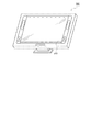
上述した表示装置1、10及び100、並びにこれらからカラーフィルタ87を省略した構成は、それぞれ、例えば、図26に示す電子機器500の表示部510に適用され得る。この電子機器500は、カーナビゲーションシステム用の表示機器である。電子機器500では、表示装置1、10若しくは100、又はこれらからカラーフィルタ87を省略した構成が適用された表示部510によって、例えば、運転席側から第1の画像として地図などの画像が視認され、助手席側から第2の画像として映画などの画像が視認され得る。
また、表示部510として表示装置1、10若しくは100、又はこれらからカラーフィルタ87を省略した構成が適用されているので、指向性表示における適視範囲119aや適視範囲119bを拡大しやすくすることができる。
The above-described
In addition, since the
さらに、電子機器500では、表示装置1、10若しくは100、又はこれらからカラーフィルタ87を省略した構成において、X方向における画素密度を高めやすくすることができるので、指向性表示における高精細化が図られる。
なお、電子機器500としては、カーナビゲーションシステム用の表示機器に限られず、携帯電話機、モバイルコンピュータ、デジタルスチルカメラ、デジタルビデオカメラ、車載機器、オーディオ機器等の種々の電子機器が挙げられる。
Further, in the
Note that the
1,10,100…表示装置、3…表示面、5,5r,5g,5b…画素、51…第1の画素、52…第2の画素、7…表示領域、11,20…素子基板、13…封止基板、25…画素群、27…選択トランジスタ、29…駆動トランジスタ、31…容量素子、33…画素電極、35…有機層、37…共通電極、39…補助配線、41…第1基板、51…第1半導体層、51a…ソース領域、51b…チャネル領域、51c…ドレイン領域、51d…電極部、53…第2半導体層、53a…ソース領域、53b…チャネル領域、53c…ドレイン領域、55…島状電極、55a…ゲート電極部、55b…電極部、57…ゲート電極部、59…ドレイン電極、65…ソース電極部、67…接続部、69…接続部、71…バンク、71a…バンク、71b…バンク、77…発光層、81…第2基板、83…遮光膜、85…開口部、87,87r,87g,87b…カラーフィルタ、93…樹脂層、95a,95b…プリズム部、97…接着剤、113…第1の範囲、115…第2の範囲、117…範囲、119a,119b…適視範囲、131…第1電極、133…第2電極、141…レンズ部、500…電子機器、510…表示部、CH1〜CH8…コンタクトホール、M…マトリクス、GT1,GT2…走査線、SI,SI1,SI2…データ線、PW…電源線。
1,10,100 ... display, 3 ... display surface, 5,5r, 5g, 5b ... pixels, 5 1 ... first pixel, 5 2 ... second pixel, 7 ... display area, 11, 20 ... devices Substrate, 13 ... sealing substrate, 25 ... pixel group, 27 ... selection transistor, 29 ... drive transistor, 31 ... capacitive element, 33 ... pixel electrode, 35 ... organic layer, 37 ... common electrode, 39 ... auxiliary wiring, 41 ...
Claims (10)
前記第1基板の第1面に設けられ、前記複数の画素の各画素において発光が制御される発光層と、
前記第1面に対向する第2面を有する第2基板と、
前記第2基板の前記第2面に設けられた遮光層と、
前記領域を囲むとともに、前記第1基板と前記第2基板の間に配置されたシール材と、
を有し、
前記複数の画素は、第1の画像を形成する第1の画素及び第2の画像を形成する第2の画素を少なくとも含んでおり、
前記遮光層には、前記第1の画素の前記発光層から前記第2基板を経て第1の範囲に及ぶ光を通すとともに、前記第2の画素の前記発光層から前記第2基板を経て第2の範囲に及ぶ光を通す開口部が設けられていることを特徴とする電気光学装置。 A first substrate having a region having a plurality of pixels ;
A light emitting layer provided on the first surface of the first substrate, the light emission of which is controlled in each pixel of the plurality of pixels;
A second substrate having a second surface opposite the first surface ;
A light shielding layer provided on the second surface of the second substrate ;
A sealant surrounding the region and disposed between the first substrate and the second substrate;
Have
The plurality of pixels include at least a first pixel that forms a first image and a second pixel that forms a second image;
The light-shielding layer passes light from the light-emitting layer of the first pixel through the second substrate through the first range, and from the light-emitting layer of the second pixel to the second substrate through the second substrate. 2. An electro-optical device characterized in that an opening for transmitting light in a range of 2 is provided.
前記発光層及び前記遮光層の間で前記発光層に対向して設けられた第2電極と、 A second electrode provided opposite to the light emitting layer between the light emitting layer and the light shielding layer;
を有し、Have
前記第1基板と前記第2基板とは、前記樹脂層と前記第2電極とが接着剤を介して接合されることを特徴とする請求項2に記載の電気光学装置。 3. The electro-optical device according to claim 2, wherein the first substrate and the second substrate have the resin layer and the second electrode bonded to each other through an adhesive.
前記スイッチング素子は、前記第1基板及び前記発光層の間に設けられていることを特徴とする請求項3に記載の電気光学装置。 A switching element that is provided corresponding to each of the pixels and switches supply and interruption of current flowing from one of the first electrode and the second electrode to the other of the first electrode and the second electrode through the light emitting layer; Have
The electro-optical device according to claim 3 , wherein the switching element is provided between the first substrate and the light emitting layer.
赤系の色を呈する光を発する前記発光層を有する赤系画素と、
緑系の色を呈する光を発する前記発光層を有する緑系画素と、
青系の色を呈する光を発する前記発光層を有する青系画素と、が含まれていることを特徴とする請求項1乃至7のいずれか一項に記載の電気光学装置。 The plurality of pixels include
A red pixel having the light emitting layer emitting light exhibiting a red color;
A green pixel having the light emitting layer emitting light exhibiting a green color;
Bluish electro-optical device according to any one of claims 1 to 7, and blue-based pixel having a light emitting layer for emitting light, characterized in that it contains exhibiting color.
緑系の色を呈する光を透過させる緑系フィルタと、
青系の色を呈する光を透過させる青系フィルタと、を有することを特徴とする請求項1乃至8のいずれか一項に記載の電気光学装置。 A red filter that transmits light having a red color; and
A green filter that transmits light of a green color; and
Bluish electro-optical device according to any one of claims 1 to 8, characterized in that it has a, and blue-based filter that transmits light exhibiting a color.
徴とする電子機器。 An electronic apparatus comprising the electro-optical device according to any one of claims 1 to 9 as a display unit.
Priority Applications (5)
| Application Number | Priority Date | Filing Date | Title |
|---|---|---|---|
| JP2008001896A JP5024059B2 (en) | 2008-01-09 | 2008-01-09 | Electro-optical device and electronic apparatus |
| KR1020090001511A KR20090076836A (en) | 2008-01-09 | 2009-01-08 | Electro-optical device and electronic apparatus |
| US12/350,342 US7894116B2 (en) | 2008-01-09 | 2009-01-08 | Electro-optical device and electronic apparatus |
| TW098100506A TW200948181A (en) | 2008-01-09 | 2009-01-08 | Electro-optical device and electronic apparatus |
| CN2009100026532A CN101483187B (en) | 2008-01-09 | 2009-01-09 | Electro-optical device and electronic apparatus |
Applications Claiming Priority (1)
| Application Number | Priority Date | Filing Date | Title |
|---|---|---|---|
| JP2008001896A JP5024059B2 (en) | 2008-01-09 | 2008-01-09 | Electro-optical device and electronic apparatus |
Publications (2)
| Publication Number | Publication Date |
|---|---|
| JP2009164027A JP2009164027A (en) | 2009-07-23 |
| JP5024059B2 true JP5024059B2 (en) | 2012-09-12 |
Family
ID=40880212
Family Applications (1)
| Application Number | Title | Priority Date | Filing Date |
|---|---|---|---|
| JP2008001896A Active JP5024059B2 (en) | 2008-01-09 | 2008-01-09 | Electro-optical device and electronic apparatus |
Country Status (2)
| Country | Link |
|---|---|
| JP (1) | JP5024059B2 (en) |
| CN (1) | CN101483187B (en) |
Families Citing this family (12)
| Publication number | Priority date | Publication date | Assignee | Title |
|---|---|---|---|---|
| JP5320267B2 (en) * | 2009-11-10 | 2013-10-23 | パナソニック株式会社 | Organic EL display |
| JP5622072B2 (en) * | 2009-12-18 | 2014-11-12 | 大日本印刷株式会社 | Color filter and organic EL display device provided with color filter |
| KR20120008359A (en) * | 2010-07-16 | 2012-01-30 | 삼성모바일디스플레이주식회사 | Organic light emitting device containing a layer with uv protectinon or other capability between an encapsulation substrate and an organic light emitting unit |
| KR102051103B1 (en) * | 2012-11-07 | 2019-12-03 | 삼성디스플레이 주식회사 | Organic light emitting diode display |
| JP6119437B2 (en) * | 2013-06-05 | 2017-04-26 | セイコーエプソン株式会社 | Electro-optical device, method of manufacturing electro-optical device, and electronic apparatus |
| KR102402605B1 (en) * | 2015-07-28 | 2022-05-27 | 삼성디스플레이 주식회사 | organic light emitting display |
| KR102400022B1 (en) * | 2015-12-30 | 2022-05-19 | 엘지디스플레이 주식회사 | Flexible Organic Light Emitting Diode Display Having Edge Bending Structure |
| DE102017100798A1 (en) | 2017-01-17 | 2018-07-19 | Osram Opto Semiconductors Gmbh | display device |
| TWI648879B (en) * | 2018-04-11 | 2019-01-21 | 友達光電股份有限公司 | Light-emitting element |
| CN111755490B (en) * | 2020-06-22 | 2022-07-29 | 武汉华星光电半导体显示技术有限公司 | Display panel |
| TWI746260B (en) | 2020-11-10 | 2021-11-11 | 友達光電股份有限公司 | Photosensitive device |
| JP2022154586A (en) * | 2021-03-30 | 2022-10-13 | 株式会社ジャパンディスプレイ | Display device |
Family Cites Families (6)
| Publication number | Priority date | Publication date | Assignee | Title |
|---|---|---|---|---|
| JP3056581B2 (en) * | 1992-02-24 | 2000-06-26 | 日本電信電話株式会社 | Projection type stereoscopic display |
| JP4176569B2 (en) * | 2003-07-22 | 2008-11-05 | 株式会社東芝 | Stereoscopic display device and image display method |
| JP4024769B2 (en) * | 2004-03-11 | 2007-12-19 | シャープ株式会社 | Liquid crystal display panel and liquid crystal display device |
| US7365494B2 (en) * | 2004-12-03 | 2008-04-29 | Semiconductor Energy Laboratory Co., Ltd. | Display device and manufacturing method thereof |
| US7518664B2 (en) * | 2005-09-12 | 2009-04-14 | Sharp Kabushiki Kaisha | Multiple-view directional display having parallax optic disposed within an image display element that has an image display layer sandwiched between TFT and color filter substrates |
| JP2007079265A (en) * | 2005-09-15 | 2007-03-29 | Sharp Corp | Display device |
-
2008
- 2008-01-09 JP JP2008001896A patent/JP5024059B2/en active Active
-
2009
- 2009-01-09 CN CN2009100026532A patent/CN101483187B/en active Active
Also Published As
| Publication number | Publication date |
|---|---|
| CN101483187B (en) | 2012-06-27 |
| CN101483187A (en) | 2009-07-15 |
| JP2009164027A (en) | 2009-07-23 |
Similar Documents
| Publication | Publication Date | Title |
|---|---|---|
| JP5024059B2 (en) | Electro-optical device and electronic apparatus | |
| US10707281B2 (en) | Display apparatus | |
| US9858847B2 (en) | Pixel array, electro optical device, electric apparatus and method of driving pixel array | |
| KR100935415B1 (en) | A display device | |
| US11088213B1 (en) | Display substrate, display apparatus, method of controlling display substrate, and method of fabricating display substrate | |
| US20160104413A1 (en) | Pixel array, electro optical device, electric apparatus and pixel rendering method | |
| US20150311265A1 (en) | Pixel array, electro-optic device, and electric apparatus | |
| KR102626690B1 (en) | Display device, method for manufacturing the same, and head mounted display including the same | |
| JP2009186876A (en) | Electrooptical device and electronic device | |
| KR100575574B1 (en) | Liquid crystal display device, electro-optical device and method of producing the same, and electronic apparatus | |
| KR102688482B1 (en) | Organic light emitting display device and head mounted display including the same | |
| KR20180077758A (en) | Organic light emitting display device | |
| US11714515B2 (en) | Display device | |
| JP2011090925A (en) | Method for manufacturing electro-optical device | |
| CN110911439B (en) | Display panel, display screen and display terminal | |
| JP2021099483A (en) | Pixel array substrate and display device having the same | |
| US7894116B2 (en) | Electro-optical device and electronic apparatus | |
| JP5223341B2 (en) | Electro-optical device and electronic apparatus | |
| KR101651521B1 (en) | Organic electro-luminescence device for medical | |
| JP5145878B2 (en) | Electro-optical device and electronic apparatus | |
| JP5304761B2 (en) | LIGHT EMITTING DEVICE AND ELECTRONIC DEVICE | |
| EP3679422B1 (en) | Display substrate and display apparatus | |
| JP2021056454A (en) | Display device | |
| US20240260429A1 (en) | Light emitting display device | |
| US20240349551A1 (en) | Display device and electronic apparatus |
Legal Events
| Date | Code | Title | Description |
|---|---|---|---|
| A621 | Written request for application examination |
Free format text: JAPANESE INTERMEDIATE CODE: A621 Effective date: 20100129 |
|
| A977 | Report on retrieval |
Free format text: JAPANESE INTERMEDIATE CODE: A971007 Effective date: 20110913 |
|
| A131 | Notification of reasons for refusal |
Free format text: JAPANESE INTERMEDIATE CODE: A131 Effective date: 20110927 |
|
| A521 | Request for written amendment filed |
Free format text: JAPANESE INTERMEDIATE CODE: A523 Effective date: 20111114 |
|
| TRDD | Decision of grant or rejection written | ||
| A01 | Written decision to grant a patent or to grant a registration (utility model) |
Free format text: JAPANESE INTERMEDIATE CODE: A01 Effective date: 20120522 |
|
| A01 | Written decision to grant a patent or to grant a registration (utility model) |
Free format text: JAPANESE INTERMEDIATE CODE: A01 |
|
| A61 | First payment of annual fees (during grant procedure) |
Free format text: JAPANESE INTERMEDIATE CODE: A61 Effective date: 20120604 |
|
| FPAY | Renewal fee payment (event date is renewal date of database) |
Free format text: PAYMENT UNTIL: 20150629 Year of fee payment: 3 |
|
| R150 | Certificate of patent or registration of utility model |
Ref document number: 5024059 Country of ref document: JP Free format text: JAPANESE INTERMEDIATE CODE: R150 |
|
| S531 | Written request for registration of change of domicile |
Free format text: JAPANESE INTERMEDIATE CODE: R313531 |
|
| R350 | Written notification of registration of transfer |
Free format text: JAPANESE INTERMEDIATE CODE: R350 |
|
| R250 | Receipt of annual fees |
Free format text: JAPANESE INTERMEDIATE CODE: R250 |
|
| R250 | Receipt of annual fees |
Free format text: JAPANESE INTERMEDIATE CODE: R250 |
|
| R250 | Receipt of annual fees |
Free format text: JAPANESE INTERMEDIATE CODE: R250 |
|
| R250 | Receipt of annual fees |
Free format text: JAPANESE INTERMEDIATE CODE: R250 |
|
| S111 | Request for change of ownership or part of ownership |
Free format text: JAPANESE INTERMEDIATE CODE: R313113 |
|
| R350 | Written notification of registration of transfer |
Free format text: JAPANESE INTERMEDIATE CODE: R350 |
|
| R250 | Receipt of annual fees |
Free format text: JAPANESE INTERMEDIATE CODE: R250 |
|
| R250 | Receipt of annual fees |
Free format text: JAPANESE INTERMEDIATE CODE: R250 |