JP5012776B2 - Light emitting device and drive control method of light emitting device - Google Patents
Light emitting device and drive control method of light emitting device Download PDFInfo
- Publication number
- JP5012776B2 JP5012776B2 JP2008305715A JP2008305715A JP5012776B2 JP 5012776 B2 JP5012776 B2 JP 5012776B2 JP 2008305715 A JP2008305715 A JP 2008305715A JP 2008305715 A JP2008305715 A JP 2008305715A JP 5012776 B2 JP5012776 B2 JP 5012776B2
- Authority
- JP
- Japan
- Prior art keywords
- voltage
- signal
- pixel
- value
- relaxation time
- Prior art date
- Legal status (The legal status is an assumption and is not a legal conclusion. Google has not performed a legal analysis and makes no representation as to the accuracy of the status listed.)
- Expired - Fee Related
Links
Images


Classifications
-
- G—PHYSICS
- G09—EDUCATION; CRYPTOGRAPHY; DISPLAY; ADVERTISING; SEALS
- G09G—ARRANGEMENTS OR CIRCUITS FOR CONTROL OF INDICATING DEVICES USING STATIC MEANS TO PRESENT VARIABLE INFORMATION
- G09G3/00—Control arrangements or circuits, of interest only in connection with visual indicators other than cathode-ray tubes
- G09G3/20—Control arrangements or circuits, of interest only in connection with visual indicators other than cathode-ray tubes for presentation of an assembly of a number of characters, e.g. a page, by composing the assembly by combination of individual elements arranged in a matrix no fixed position being assigned to or needed to be assigned to the individual characters or partial characters
- G09G3/22—Control arrangements or circuits, of interest only in connection with visual indicators other than cathode-ray tubes for presentation of an assembly of a number of characters, e.g. a page, by composing the assembly by combination of individual elements arranged in a matrix no fixed position being assigned to or needed to be assigned to the individual characters or partial characters using controlled light sources
- G09G3/30—Control arrangements or circuits, of interest only in connection with visual indicators other than cathode-ray tubes for presentation of an assembly of a number of characters, e.g. a page, by composing the assembly by combination of individual elements arranged in a matrix no fixed position being assigned to or needed to be assigned to the individual characters or partial characters using controlled light sources using electroluminescent panels
- G09G3/32—Control arrangements or circuits, of interest only in connection with visual indicators other than cathode-ray tubes for presentation of an assembly of a number of characters, e.g. a page, by composing the assembly by combination of individual elements arranged in a matrix no fixed position being assigned to or needed to be assigned to the individual characters or partial characters using controlled light sources using electroluminescent panels semiconductive, e.g. using light-emitting diodes [LED]
- G09G3/3208—Control arrangements or circuits, of interest only in connection with visual indicators other than cathode-ray tubes for presentation of an assembly of a number of characters, e.g. a page, by composing the assembly by combination of individual elements arranged in a matrix no fixed position being assigned to or needed to be assigned to the individual characters or partial characters using controlled light sources using electroluminescent panels semiconductive, e.g. using light-emitting diodes [LED] organic, e.g. using organic light-emitting diodes [OLED]
- G09G3/3275—Details of drivers for data electrodes
- G09G3/3291—Details of drivers for data electrodes in which the data driver supplies a variable data voltage for setting the current through, or the voltage across, the light-emitting elements
-
- G—PHYSICS
- G09—EDUCATION; CRYPTOGRAPHY; DISPLAY; ADVERTISING; SEALS
- G09G—ARRANGEMENTS OR CIRCUITS FOR CONTROL OF INDICATING DEVICES USING STATIC MEANS TO PRESENT VARIABLE INFORMATION
- G09G2300/00—Aspects of the constitution of display devices
- G09G2300/08—Active matrix structure, i.e. with use of active elements, inclusive of non-linear two terminal elements, in the pixels together with light emitting or modulating elements
- G09G2300/0809—Several active elements per pixel in active matrix panels
- G09G2300/0842—Several active elements per pixel in active matrix panels forming a memory circuit, e.g. a dynamic memory with one capacitor
-
- G—PHYSICS
- G09—EDUCATION; CRYPTOGRAPHY; DISPLAY; ADVERTISING; SEALS
- G09G—ARRANGEMENTS OR CIRCUITS FOR CONTROL OF INDICATING DEVICES USING STATIC MEANS TO PRESENT VARIABLE INFORMATION
- G09G2320/00—Control of display operating conditions
- G09G2320/04—Maintaining the quality of display appearance
- G09G2320/043—Preventing or counteracting the effects of ageing
-
- G—PHYSICS
- G09—EDUCATION; CRYPTOGRAPHY; DISPLAY; ADVERTISING; SEALS
- G09G—ARRANGEMENTS OR CIRCUITS FOR CONTROL OF INDICATING DEVICES USING STATIC MEANS TO PRESENT VARIABLE INFORMATION
- G09G3/00—Control arrangements or circuits, of interest only in connection with visual indicators other than cathode-ray tubes
- G09G3/20—Control arrangements or circuits, of interest only in connection with visual indicators other than cathode-ray tubes for presentation of an assembly of a number of characters, e.g. a page, by composing the assembly by combination of individual elements arranged in a matrix no fixed position being assigned to or needed to be assigned to the individual characters or partial characters
- G09G3/22—Control arrangements or circuits, of interest only in connection with visual indicators other than cathode-ray tubes for presentation of an assembly of a number of characters, e.g. a page, by composing the assembly by combination of individual elements arranged in a matrix no fixed position being assigned to or needed to be assigned to the individual characters or partial characters using controlled light sources
- G09G3/30—Control arrangements or circuits, of interest only in connection with visual indicators other than cathode-ray tubes for presentation of an assembly of a number of characters, e.g. a page, by composing the assembly by combination of individual elements arranged in a matrix no fixed position being assigned to or needed to be assigned to the individual characters or partial characters using controlled light sources using electroluminescent panels
- G09G3/32—Control arrangements or circuits, of interest only in connection with visual indicators other than cathode-ray tubes for presentation of an assembly of a number of characters, e.g. a page, by composing the assembly by combination of individual elements arranged in a matrix no fixed position being assigned to or needed to be assigned to the individual characters or partial characters using controlled light sources using electroluminescent panels semiconductive, e.g. using light-emitting diodes [LED]
- G09G3/3208—Control arrangements or circuits, of interest only in connection with visual indicators other than cathode-ray tubes for presentation of an assembly of a number of characters, e.g. a page, by composing the assembly by combination of individual elements arranged in a matrix no fixed position being assigned to or needed to be assigned to the individual characters or partial characters using controlled light sources using electroluminescent panels semiconductive, e.g. using light-emitting diodes [LED] organic, e.g. using organic light-emitting diodes [OLED]
- G09G3/3225—Control arrangements or circuits, of interest only in connection with visual indicators other than cathode-ray tubes for presentation of an assembly of a number of characters, e.g. a page, by composing the assembly by combination of individual elements arranged in a matrix no fixed position being assigned to or needed to be assigned to the individual characters or partial characters using controlled light sources using electroluminescent panels semiconductive, e.g. using light-emitting diodes [LED] organic, e.g. using organic light-emitting diodes [OLED] using an active matrix
- G09G3/3233—Control arrangements or circuits, of interest only in connection with visual indicators other than cathode-ray tubes for presentation of an assembly of a number of characters, e.g. a page, by composing the assembly by combination of individual elements arranged in a matrix no fixed position being assigned to or needed to be assigned to the individual characters or partial characters using controlled light sources using electroluminescent panels semiconductive, e.g. using light-emitting diodes [LED] organic, e.g. using organic light-emitting diodes [OLED] using an active matrix with pixel circuitry controlling the current through the light-emitting element
Description
本発明は、発光装置、及び発光装置の駆動制御方法に関するものである。 The present invention relates to a light emitting device and a drive control method for the light emitting device.
近年、液晶表示装置に続く次世代の表示デバイスとして、発光素子をマトリクス状に配列した表示パネル(画素アレイ)を備えた発光素子型の表示装置(発光素子型ディスプレイ、発光装置)の研究開発が盛んに行われている。 In recent years, as a next-generation display device following a liquid crystal display device, research and development of a light-emitting element type display device (light-emitting element type display, light-emitting device) provided with a display panel (pixel array) in which light-emitting elements are arranged in a matrix form has been conducted. It is actively done.
このような発光素子としては、有機エレクトロルミネッセンス素子(有機EL素子)や無機エレクトロルミネッセンス素子(無機EL素子)、あるいは、発光ダイオード(LED)等のような電流駆動型の発光素子がある。 Examples of such a light emitting element include an organic electroluminescent element (organic EL element), an inorganic electroluminescent element (inorganic EL element), and a current driven light emitting element such as a light emitting diode (LED).
特に、アクティブマトリクス駆動方式を適用した発光素子型の表示装置においては、周知の液晶表示装置と比較して、表示応答速度が速く、また、視野角依存性もなく、高輝度・高コントラスト化、表示画質の高精細化等が可能である。 In particular, in a light emitting element type display device to which an active matrix driving method is applied, the display response speed is faster than that of a known liquid crystal display device, and there is no viewing angle dependency, resulting in high brightness and high contrast. The display image quality can be increased.
それとともに、発光素子型の表示装置は、液晶表示装置のようにバックライトや導光板を必要としないので、一層の薄型軽量化が可能であるという極めて優位な特徴を有している。そのため、今後様々な電子機器への適用が期待されている。 At the same time, the light emitting element type display device does not require a backlight or a light guide plate unlike a liquid crystal display device, and thus has an extremely advantageous feature that it can be further reduced in thickness and weight. Therefore, application to various electronic devices is expected in the future.
このような発光素子型の表示装置として、例えば、電圧信号によって電流制御されたアクティブマトリクス駆動方式の表示装置としての有機ELディスプレイ装置がある(例えば、特許文献1参照)。 As such a light emitting element type display device, for example, there is an organic EL display device as an active matrix driving type display device in which current is controlled by a voltage signal (see, for example, Patent Document 1).
この有機ELディスプレイ装置では、発光素子としての有機EL素子と、有機EL素子を駆動するための電流制御用薄膜トランジスタとスイッチ用薄膜トランジスタとを有する画素駆動回路とが、各画素に設けられている。 In this organic EL display device, each pixel is provided with an organic EL element as a light emitting element, and a pixel driving circuit having a current control thin film transistor and a switching thin film transistor for driving the organic EL element.
電流制御用薄膜トランジスタは、画像データに応じた電圧値を有する電圧信号がゲートに印加され、このゲート電圧で電流制御用薄膜トランジスタのドレイン−ソース間に流れる電流の電流値を制御し、この電流を有機EL素子に供給して発光させる。スイッチ用薄膜トランジスタは、この電流制御用薄膜トランジスタのゲートに画像データに応じた電圧信号を供給するためのスイッチングを行う。 In the thin film transistor for current control, a voltage signal having a voltage value corresponding to image data is applied to the gate, the current value of the current flowing between the drain and source of the thin film transistor for current control is controlled by this gate voltage, and this current is The light is supplied to the EL element to emit light. The switch thin film transistor performs switching for supplying a voltage signal corresponding to image data to the gate of the current control thin film transistor.
しかしながら、各画素の電流制御用薄膜トランジスタの特性が使用時に経時的に変化することがある。特に、電流制御用薄膜トランジスタがアモルファスシリコンTFTからなる場合には、その閾値電圧Vthの経時的な変化が比較的大きいことが知られている。 However, the characteristics of the current control thin film transistor of each pixel may change over time during use. In particular, when the current control thin film transistor is made of an amorphous silicon TFT, it is known that a change with time of the threshold voltage Vth is relatively large.
電圧信号の電圧値によって階調を制御する構成においては、閾値電圧Vthが変化すると同じゲート電圧を印加してもドレイン−ソース間に流れる電流の電流値が変化してしまい、有機EL素子の発光輝度が変化してしまう。 In the configuration in which the gradation is controlled by the voltage value of the voltage signal, even if the same gate voltage is applied when the threshold voltage Vth changes, the current value of the current flowing between the drain and source changes, and the light emission of the organic EL element The brightness will change.
また、電流制御用薄膜トランジスタのドレイン−ソース間に流れる電流の電流値は電流増幅率βの値に比例する。このため、各画素の電流制御用薄膜トランジスタの閾値電圧が同じであっても、例えば製造プロセスに起因して電流増幅率βの値がばらついていると、電流制御用薄膜トランジスタのドレイン−ソース間に流れる電流の電流値にバラツキが生じ、有機EL素子の発光輝度がばらついてしまう。 The current value of the current flowing between the drain and source of the current control thin film transistor is proportional to the value of the current amplification factor β. For this reason, even if the threshold voltage of the current control thin film transistor of each pixel is the same, for example, if the value of the current amplification factor β varies due to the manufacturing process, the current control thin film transistor flows between the drain and source of the current control thin film transistor. The current value varies, and the light emission luminance of the organic EL element varies.
この移動度のバラツキは特に低温ポリシリコンTFTに顕著であり、それに比べてアモルファスシリコンTFTではバラツキは比較的少ない。しかし、それでも製造プロセス起因のバラツキによる影響は避けられない。 This variation in mobility is particularly noticeable in low-temperature polysilicon TFTs, and in contrast, there is relatively little variation in amorphous silicon TFTs. However, the effects of variations due to the manufacturing process are still inevitable.
このように、閾値電圧Vthの変化や、電流増幅率βのバラツキは、画質に影響する。従って、このような閾値電圧Vthの変化や、電流増幅率βのバラツキによる画質の劣化を抑制するためには、特性パラメータとして、例えば、各画素に対応する閾値電圧及び電流増幅率βとそのバラツキ量を取得して、供給された画像データに応じて各画素に供給する電圧信号をこの特性パラメータに基づいて補正する必要がある。 Thus, the change in the threshold voltage Vth and the variation in the current amplification factor β affect the image quality. Therefore, in order to suppress the deterioration of the image quality due to the change of the threshold voltage Vth and the variation of the current amplification factor β, for example, as the characteristic parameter, the threshold voltage and the current amplification factor β corresponding to each pixel and the variation thereof are used. It is necessary to acquire the amount and correct the voltage signal supplied to each pixel based on the supplied image data based on this characteristic parameter.
本発明は、このような従来の問題点に鑑みてなされたもので、各画素の特性パラメータ及びそのバラツキ量を取得して、供給された画像データに応じた電圧信号の電圧値を補正することが可能な発光装置及び発光装置の駆動制御方法を提供することを目的とする。 The present invention has been made in view of such conventional problems, and obtains the characteristic parameter of each pixel and the amount of variation thereof, and corrects the voltage value of the voltage signal in accordance with the supplied image data. It is an object of the present invention to provide a light emitting device capable of performing the above and a drive control method for the light emitting device.
この目的を達成するため、本発明の第1の観点に係る発光装置は、
複数の画素と、該各画素に接続された複数の信号線と、を有し、前記各画素は、電流が供給されて発光する発光素子と、前記各信号線の一端に接続されて、前記発光素子に供給する電流を制御する駆動素子と該駆動素子に印加された電圧に対応する電荷を蓄積する保持容量とを有する画素駆動回路と、を備える画素アレイと、
供給される画像データに応じた駆動信号を、前記各信号線を介して前記各画素に印加する信号線駆動部と、
を備え、
前記信号線駆動部は、
前記各画素の前記駆動素子の閾値電圧を超える電圧値を有する基準電圧を出力する電圧印加部と、
前記各信号線の他端の電圧を測定電圧として取得する電圧測定部と、
前記電圧発生部の出力端と前記各信号線の他端との接続を切り換え、前記信号線の他端と前記電圧印加部を接続して該信号線の他端に前記基準電圧を所定時間印加した後、前記信号線の他端を、前記電圧印加部との接続が遮断された状態に設定する切換部と、
前記切換部により前記信号線の他端が前記電圧印加部との接続が遮断された状態に設定された時点から、予め設定された複数の異なる緩和時間が経過した後に前記電圧測定部により取得される、複数の前記測定電圧の値に基づく特性パラメータを取得する特性パラメータ取得部と、
前記特性パラメータに基づいて、前記画像データに応じた電圧信号の電圧値を補正した補正電圧信号を生成する電圧信号補正部と、
前記補正電圧信号に基づいて前記駆動信号を生成して、前記各信号線の他端に印加する駆動信号印加部と、
を備え、
前記特性パラメータ取得部は、
容量成分C[F]を、前記信号線に寄生する寄生容量と前記保持容量と前記発光素子に寄生する発光素子容量との合計とし、前記画素駆動回路の電流増幅率の設計値をβ0[A/V 2 ]とし、前記緩和時間をt[sec]としたとき、(C/β0)/t<1[V]となる時間でより大きい複数の異なる時間[sec]値に設定される第1の緩和時間群において、前記電圧測定部により取得される複数の前記測定電圧の値に基づいて、前記各画素の前記駆動素子の第1の閾値電圧と前記画素駆動回路の電流増幅率とを、前記特性パラメータにおける第1の特性パラメータとして算出して取得し、
前記複数の画素における前記容量成分と算出された前記電流増幅率との比率(C/β0)の平均値と、(C/β0)/t≧1[V]となる時間に設定される第2の緩和時間において前記電圧測定部により取得される前記測定電圧の値と、前記各画素の前記第1の閾値電圧の値と、に基づいて、前記電流増幅率の、該電流増幅率の設計値β0に対する偏差をΔβとしたとき、前記偏差Δβの前記電流増幅率の設計値β0に対する比率(Δβ/β0)であるバラツキパラメータを、前記特性パラメータにおける第2の特性パラメータとして算出して取得し、
前記電圧信号補正部は、前記画像データに応じた電圧信号をVdata0、前記補正電圧信号をVdata1、前記バラツキパラメータを(Δβ/β0)としたとき、式(1)に基づいて、前記補正電圧信号を算出する、ことを特徴とする。

A plurality of pixels, and a plurality of signal lines connected to the respective pixels, wherein each of the pixels is connected to a light emitting element that emits light when supplied with a current, and one end of each of the signal lines, A pixel array comprising: a drive element that controls a current supplied to the light-emitting element; and a pixel drive circuit having a storage capacitor that accumulates a charge corresponding to a voltage applied to the drive element;
A signal line drive unit that applies a drive signal corresponding to the supplied image data to each pixel via each signal line;
With
The signal line driver is
A voltage applying unit that outputs a reference voltage having a voltage value exceeding a threshold voltage of the driving element of each pixel;
A voltage measurement unit that obtains the voltage at the other end of each signal line as a measurement voltage;
Switch the connection between the output end of the voltage generator and the other end of each signal line, connect the other end of the signal line and the voltage application unit, and apply the reference voltage to the other end of the signal line for a predetermined time After that, the switching unit for setting the other end of the signal line in a state where the connection with the voltage application unit is cut off,
Acquired by the voltage measurement unit after a plurality of different relaxation times set in advance from the time when the switching unit sets the other end of the signal line to the state where the connection with the voltage application unit is cut off. A characteristic parameter acquisition unit that acquires characteristic parameters based on a plurality of values of the measurement voltage;
A voltage signal correction unit that generates a correction voltage signal obtained by correcting the voltage value of the voltage signal according to the image data based on the characteristic parameter;
A drive signal applying unit that generates the drive signal based on the correction voltage signal and applies the drive signal to the other end of each signal line;
With
The characteristic parameter acquisition unit
The capacitance component C [F] is the sum of the parasitic capacitance parasitic on the signal line, the storage capacitor, and the light emitting element capacitance parasitic on the light emitting element, and the design value of the current amplification factor of the pixel driving circuit is β0 [A / V 2 ], and when the relaxation time is t [sec], the time is set to ( C / β 0 ) / t <1 [V], and the first is set to a plurality of different different time [sec] values. In the relaxation time group, based on a plurality of values of the measurement voltage acquired by the voltage measurement unit, the first threshold voltage of the drive element of each pixel and the current amplification factor of the pixel drive circuit, Calculated and obtained as the first characteristic parameter in the characteristic parameter,
An average value of the ratio (C / β0) between the capacitance component and the calculated current amplification factor in the plurality of pixels, and a second time set as (C / β0) / t ≧ 1 [V] . Based on the value of the measurement voltage acquired by the voltage measurement unit during the relaxation time and the value of the first threshold voltage of each pixel, the design value of the current amplification factor of the current amplification factor When a deviation with respect to β0 is Δβ, a variation parameter that is a ratio (Δβ / β0) of the deviation Δβ to the design value β0 of the current amplification factor is calculated and obtained as a second characteristic parameter ;
When the voltage signal according to the image data is Vdata0, the correction voltage signal is Vdata1, and the variation parameter is (Δβ / β0), the voltage signal correction unit is configured to calculate the correction voltage signal based on Equation (1). Is calculated .
前記画素アレイにおける前記複数の信号線は第1の方向に沿って配列され、
該画素アレイは、前記第1の方向に直交する第2の方向に沿って配列される複数の走査線を有して、前記複数の画素は前記複数の走査線と前記複数の信号線の各交点近傍に配設され、
前記各走査線に選択信号を順次印加して、各行の前記各画素を順次選択状態に設定する選択駆動部を有し、
前記信号線駆動部の前記特性パラメータ取得部は、前記各信号線を介して、前記選択状態とされた行に対応する前記各画素の前記第1の特性パラメータ及び前記第2の特性パラメータを取得し、
前記駆動信号印加部は、前記選択状態とされた行に対応する前記各画素に、前記各信号線を介して、前記駆動信号を印加するようにしてもよい。
The plurality of signal lines in the pixel array are arranged along a first direction,
The pixel array has a plurality of scanning lines arranged along a second direction orthogonal to the first direction, and the plurality of pixels are each of the plurality of scanning lines and the plurality of signal lines. Arranged near the intersection,
A selection driver that sequentially applies a selection signal to each of the scanning lines and sequentially sets the pixels in each row to a selected state;
The characteristic parameter acquisition unit of the signal line driving unit acquires the first characteristic parameter and the second characteristic parameter of each pixel corresponding to the selected row via each signal line. And
The drive signal applying unit may apply the drive signal to each pixel corresponding to the selected row via each signal line.
前記画素駆動回路は、少なくとも、
電流路の一端に所定の電源電圧が印加され、該電流路の他端に前記発光素子との接続接点が接続された第1の薄膜トランジスタと、
制御端子が前記走査線に接続され、電流路の一端が前記第1の薄膜トランジスタの電流路の一端に接続され、該電流路の他端が前記第1の薄膜トランジスタの制御端子に接続された第2の薄膜トランジスタと、
を備え、
前記駆動素子は、前記第1の薄膜トランジスタであり、
前記選択状態において、前記第2の薄膜トランジスタがオン状態となって、前記第1の薄膜トランジスタの電流路の一端と制御端子とが接続され、
前記選択状態とされた行の前記各画素の前記接続点に、前記電圧印加部より印加される前記基準電圧に応じた電圧が、前記各信号線を介して印加され、
前記電圧測定部は、前記選択状態とされた行の前記各画素の前記接続点の、前記各緩和時間経過後の電圧を、前記各信号線を介して、前記測定電圧として取得するようにしてもよい。
The pixel driving circuit includes at least
A first thin film transistor in which a predetermined power supply voltage is applied to one end of the current path, and a connection contact with the light emitting element is connected to the other end of the current path;
A control terminal is connected to the scanning line, one end of the current path is connected to one end of the current path of the first thin film transistor, and the other end of the current path is connected to the control terminal of the first thin film transistor. A thin film transistor of
With
The drive element is the first thin film transistor;
In the selected state, the second thin film transistor is turned on, and one end of the current path of the first thin film transistor and the control terminal are connected,
A voltage corresponding to the reference voltage applied from the voltage application unit is applied to the connection point of each pixel of the row in the selected state via each signal line,
The voltage measurement unit obtains the voltage after the relaxation time has elapsed as the measurement voltage via the signal lines at the connection point of the pixels in the selected row. Also good.
前記特性パラメータ取得部における前記第1の特性パラメータ及び第2の特性パラメータの取得は、前記各画素の前記駆動素子が初期の特性を有している初期状態のときに実行され、
前記電圧信号補正部による前記電圧信号の補正、及び、前記駆動信号印加部による前記駆動信号の生成は、前記画像データが供給されて前記各画素を駆動する実動作時に実行されるようにしてもよい。
The acquisition of the first characteristic parameter and the second characteristic parameter in the characteristic parameter acquisition unit is executed in an initial state in which the driving element of each pixel has an initial characteristic,
The correction of the voltage signal by the voltage signal correction unit and the generation of the drive signal by the drive signal application unit may be performed during an actual operation in which the image data is supplied and the pixels are driven. Good.
前記特性パラメータ取得部は、前記第1の緩和時間群をt1[sec]、t2[sec]、該第1の緩和時間群に対応する前記測定電圧をVmeas(t1)[V]、Vmeas(t2)[V]、前記第1の閾値電圧をVth1[V]、前記電流増幅率をβ[A/V 2 ]とし、前記2つの測定電圧の値と前記2つの緩和時間の値とを式(2)に代入して演算を行うことにより、前記第1の特性パラメータを算出して取得するようにしてもよい。
The characteristic parameter acquisition unit defines the first relaxation time group as t1 [sec] and t2 [sec] , and the measurement voltage corresponding to the first relaxation time group as Vmeas (t1) [V] and Vmeas (t2 ) [V] , where the first threshold voltage is Vth1 [V] , the current amplification factor is β [A / V 2 ], and the two measured voltage values and the two relaxation time values The first characteristic parameter may be calculated and acquired by substituting into 2 ) and performing an operation.
前記特性パラメータ取得部は、前記第2の緩和時間をt3[sec]、該第2の緩和時間に対応する前記測定電圧をVmeas(t3)[V]、前記基準電圧の電圧値をVref[V]、前記各画素における前記第1の閾値電圧をVth1[V]、前記複数の画素における前記容量成分と前記電流増幅率との比率の平均値を<C/β>、前記バラツキパラメータをΔβ/β0としたとき、式(3)に基づいて、前記第2の特性パラメータを算出して取得するようにしてもよい。
前記駆動信号印加部は、前記(C/β0)/t<1[V]となる時間に設定される第3の緩和時間をt4[sec]、該第3の緩和時間に対応する前記測定電圧をVmeas(t4)[V]、前記複数の画素における前記容量成分と前記電流増幅率との比率の平均値を<C/β>、このときの前記各画素の閾値電圧を第2の閾値電圧Vth2[V]としたとき、式(4)に基づいて、前記第2の閾値電圧を算出するようにしてもよい。
![]()
![]()
前記駆動信号印加部は、前記複数の画素における前記容量成分と前記電流増幅率との比率の平均値と前記第3の緩和時間との比率(<C/β>/t4)をオフセット電圧として記憶する記憶部を有し、
前記第3の緩和時間に対応する前記測定電圧と前記記憶部に記憶された前記オフセット電圧との差分を、このときの前記各画素の前記第2の閾値電圧としてもよい。
The drive signal applying unit stores, as an offset voltage, a ratio (<C / β> / t4) between an average value of the ratio between the capacitance component and the current amplification factor in the plurality of pixels and the third relaxation time. A storage unit
A difference between the measured voltage corresponding to the third relaxation time and the offset voltage stored in the storage unit may be used as the second threshold voltage of each pixel at this time.
前記駆動信号印加部は、前記補正電圧信号と前記第2の閾値電圧とを加算した信号を前記駆動信号とするようにしてもよい。 The drive signal applying unit may use a signal obtained by adding the correction voltage signal and the second threshold voltage as the drive signal.
本発明の第2の観点に係る発光装置の駆動制御方法は、
複数の画素と、該各画素に接続された複数の信号線と、を有し、前記各画素は、電流が供給されて発光する発光素子と、前記各信号線の一端に接続されて、前記発光素子に供給する電流を制御する駆動素子と該駆動素子に印加された電圧に対応する電荷を蓄積する保持容量とを有する画素駆動回路と、を備える画素アレイを備える発光装置を、供給される画像データに応じて駆動制御する発光装置の駆動制御方法であって、
前記複数の信号線の各々の他端に電圧印加部を接続して、所定の電圧値を有する基準電圧を前記各信号線の他端に印加して、前記各画素の前記駆動素子に、該駆動素子の閾値電圧を超える電圧値を有する基準電圧を印加するステップと、
前記各信号線の他端と前記電圧印加部との接続を遮断した後、複数の異なる緩和時間が経過した後の前記各信号線の他端の電圧を、複数の測定電圧として取得するステップと、
容量成分C[F]を、前記信号線に寄生する寄生容量と前記保持容量と前記発光素子に寄生する発光素子容量との合計とし、前記画素駆動回路の電流増幅率の設計値をβ0[A/V 2 ]とし、前記緩和時間をt[sec]としたとき、(C/β0)/t<1[V]となる時間で複数の異なる時間[sec]に設定される第1の緩和時間において、前記電圧測定部により取得される2つの前記測定電圧の値に基づいて、前記各画素の前記駆動素子の第1の閾値電圧と前記画素駆動回路の電流増幅率とを第1の特性パラメータとして算出して取得するステップと、
前記複数の画素における前記容量成分と算出された前記電流増幅率との比率(C/β)の平均値と、(C/β0)/t≧1[V]となる時間に設定される第2の緩和時間において前記電圧測定部により取得される前記測定電圧の値と、前記各画素の前記第1の閾値電圧の値と、に基づいて、前記電流増幅率の、該電流増幅率の設計値β0に対する偏差をΔβとしたとき、前記偏差Δβの前記電流増幅率の設計値β0に対する比率(Δβ/β0)であるバラツキパラメータを第2の特性パラメータとして算出して取得するステップと、
前記特性パラメータ取得部が取得した前記第2の特性パラメータに基づいて、前記画像データに応じた電圧信号の電圧値を補正した補正電圧信号を生成するステップと、
前記(C/β0)/t<1[V]となる時間に設定される第3の緩和時間において前記電圧測定部により取得される前記測定電圧と、前記容量成分と前記電流増幅率との比率の平均値と、前記補正電圧信号と、に基づいて前記駆動信号を生成して、前記各信号線の他端に印加するステップと、を含む、
前記補正電圧信号を生成するステップは、前記画像データに応じた電圧信号をVdata0、前記補正電圧信号をVdata1、前記バラツキパラメータを(Δβ/β0)としたとき、式(5)に基づいて、前記補正電圧信号を算出するステップを含む、ことを特徴とする。
A plurality of pixels, and a plurality of signal lines connected to the respective pixels, wherein each of the pixels is connected to a light emitting element that emits light when supplied with a current, and one end of each of the signal lines, A light emitting device including a pixel array including a pixel driving circuit having a driving element for controlling a current supplied to the light emitting element and a storage capacitor for storing a charge corresponding to a voltage applied to the driving element is supplied. A drive control method of a light emitting device that performs drive control according to image data,
A voltage application unit is connected to the other end of each of the plurality of signal lines, a reference voltage having a predetermined voltage value is applied to the other end of each signal line, and the drive element of each pixel has the Applying a reference voltage having a voltage value exceeding a threshold voltage of the driving element;
Obtaining the voltage at the other end of each signal line after a plurality of different relaxation times have passed as a plurality of measurement voltages after disconnecting the connection between the other end of each signal line and the voltage application unit; ,
The capacitance component C [F] is the sum of the parasitic capacitance parasitic on the signal line, the storage capacitor, and the light emitting element capacitance parasitic on the light emitting element, and the design value of the current amplification factor of the pixel driving circuit is β0 [A / V 2 ], and when the relaxation time is t [sec], the first relaxation time is set to a plurality of different times [sec] with ( C / β0 ) / t <1 [V]. In the first characteristic parameter, the first threshold voltage of the driving element of each pixel and the current amplification factor of the pixel driving circuit are set to a first characteristic parameter based on two measurement voltage values acquired by the voltage measuring unit. Calculating and obtaining as:
An average value of the ratio (C / β) between the capacitance component and the calculated current amplification factor in the plurality of pixels, and a second time set as (C / β0) / t ≧ 1 [V] . Based on the value of the measurement voltage acquired by the voltage measurement unit during the relaxation time and the value of the first threshold voltage of each pixel, the design value of the current amplification factor of the current amplification factor calculating and obtaining a variation parameter, which is a ratio (Δβ / β0) of the deviation Δβ to the design value β0 of the current amplification factor as a second characteristic parameter , where Δβ is a deviation from β0 ;
Generating a corrected voltage signal by correcting the voltage value of the voltage signal according to the image data based on the second characteristic parameter acquired by the characteristic parameter acquisition unit;
Ratio of the measurement voltage acquired by the voltage measurement unit in the third relaxation time set to the time when ( C / β0 ) / t <1 [V], and the capacitance component and the current amplification factor Generating the drive signal based on an average value of the correction voltage signal and applying the correction signal to the other end of each signal line.
The step of generating the correction voltage signal is based on the equation (5) when the voltage signal corresponding to the image data is Vdata0, the correction voltage signal is Vdata1, and the variation parameter is (Δβ / β0). And a step of calculating a correction voltage signal .
前記第1の特性パラメータを取得するステップは、
前記2つの第1の緩和時間群をt1[sec]、t2[sec]、該第1の緩和時間群に対応する前記測定電圧をVmeas(t1)[V]、Vmeas(t2)[V]、前記第1の閾値電圧をVth1[V]、前記電流増幅率をβ[A/V 2 ]とし、前記2つの測定電圧の値と前記2つの緩和時間の値とを式(6)に代入して演算を行うことにより、前記第1の特性パラメータを算出して取得するステップを含むものであってもよい。
The two first relaxation time groups are t1 [sec] and t2 [sec] , and the measured voltages corresponding to the first relaxation time groups are Vmeas (t1) [V] , Vmeas (t2) [V] , The first threshold voltage is Vth1 [V] , the current amplification factor is β [A / V 2 ], and the two measured voltage values and the two relaxation time values are substituted into equation ( 6 ). And calculating and obtaining the first characteristic parameter by performing an operation.
前記第1の特性パラメータを取得するステップは、
前記第2の緩和時間をt3[sec]、該第2の緩和時間に対応する前記測定電圧をVmeas(t3)[V]、前記基準電圧の電圧値をVref[V]、前記各画素における前記第1の閾値電圧をVth1[V]、前記複数の画素における前記容量成分と前記電流増幅率との比率の平均値を<C/β>、前記バラツキパラメータをΔβ/β0としたとき、式(7)に基づいて、前記第2の特性パラメータを算出して取得するステップを含むものであってもよい。
The second relaxation time is t3 [sec] , the measurement voltage corresponding to the second relaxation time is Vmeas (t3) [V] , the voltage value of the reference voltage is Vref [V] , and the voltage in each pixel is the first threshold voltage Vth1 [V], the average value of the ratio between the capacitance component and the current amplification factor of the plurality of pixels <C / β>, when the variation parameter was Δβ /
前記駆動信号を生成して前記各信号線の他端に印加するステップは、
前記第3の緩和時間をt4[sec]、該第3の緩和時間に対応する前記測定電圧をVmeas(t4)[V]、前記複数の画素における前記容量成分と前記電流増幅率との比率の平均値を<C/β>、このときの前記各画素の閾値電圧を第2の閾値電圧Vth2[V]としたとき、式(8)に基づいて、前記第2の閾値電圧を算出するステップを含むものであってもよい。
![]()
The third relaxation time is t4 [sec] , the measurement voltage corresponding to the third relaxation time is Vmeas (t4) [V] , and the ratio between the capacitance component and the current amplification factor in the plurality of pixels is Step of calculating the second threshold voltage based on the equation (8), where the average value is <C / β> and the threshold voltage of each pixel at this time is the second threshold voltage Vth2 [V] . May be included.
![]()
前記駆動信号を生成して前記各信号線の他端に印加するステップは、
前記複数の画素における前記容量成分と前記電流増幅率との比率の平均値と前記第3の緩和時間との比率(<C/β>/t4)をオフセット電圧として記憶するステップと、
前記第3の緩和時間に対応する前記測定電圧と前記記憶された前記オフセット電圧との差分を、このときの前記各画素の第2の閾値電圧とするステップを含むものであってもよい。
The step of generating the drive signal and applying it to the other end of each signal line includes:
Storing an average value of a ratio between the capacitance component and the current amplification factor in the plurality of pixels and a ratio of the third relaxation time (<C / β> / t4) as an offset voltage;
A step of setting a difference between the measured voltage corresponding to the third relaxation time and the stored offset voltage as a second threshold voltage of each pixel at this time may be included.
前記駆動信号を生成して前記各信号線の他端に印加するステップは、
前記補正電圧信号と前記第2の閾値電圧とを加算した信号を前記駆動信号として、前記各信号線の他端に印加するステップを含むものであってもよい。
The step of generating the drive signal and applying it to the other end of each signal line includes:
A step of applying a signal obtained by adding the correction voltage signal and the second threshold voltage to the other end of each signal line as the drive signal may be included.
本発明によれば、各画素の特性パラメータやそのバラツキを取得して、供給された画像データを補正することができる。また、画質の劣化を抑制することができる。 According to the present invention, it is possible to correct the supplied image data by acquiring the characteristic parameters of each pixel and their variations. In addition, deterioration of image quality can be suppressed.
以下、本発明の実施形態に係る発光装置を図面を参照して説明する。尚、本実施形態では、発光装置を表示装置として説明する。
本実施形態に係る表示装置の構成を図1に示す。
本実施形態に係る表示装置(発光装置)1は、パネルモジュール11と、アナログ電源(電圧印加部)14と、ロジック電源15と、制御部(パラメータ取得部、電圧信号補正部)16と、によって構成される。
Hereinafter, a light emitting device according to an embodiment of the present invention will be described with reference to the drawings. In the present embodiment, the light emitting device is described as a display device.
The configuration of the display device according to the present embodiment is shown in FIG.
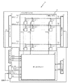
A display device (light emitting device) 1 according to the present embodiment includes a
パネルモジュール11は、有機ELパネル(画素アレイ)21とデータドライバ(信号線駆動部)22とアノード回路(電源駆動部)12とセレクトドライバ(選択駆動部)13とを備える。
The
有機ELパネル21は、列方向に配設される複数のデータライン(信号線)Ldi(i=1〜m)と、行方向に配設される複数のセレクトライン(走査線)Lsj(j=1〜n)と、行方向に配設される複数のアノードラインLaと、複数の画素21(i,j)(i=1〜m、j=1〜n、m、n;自然数)と、を備える。画素21(i,j)はデータラインLdiとセレクトラインLsjとの交点近傍に配列される。
The
図1に示すパネルモジュール11の構成の詳細を図2に示す。各画素21(i,j)は、画像の1画素に対応するものであり、図2に示すように、有機EL素子(発光素子)101と、トランジスタT1〜T3と、ストレージ容量(保持容量)Csとからなる画素駆動回路DCと、を備える。
Details of the configuration of the
有機EL(Organic Electro-Luminescence)素子101は、有機化合物に注入された電子と正孔との再結合によって生じた励起子によって発光する現象を利用した自発光型の表示素子であり、供給された電流の電流値に対応する輝度で発光する。
An organic EL (Organic Electro-Luminescence)
有機EL素子101には、画素電極が形成され、この画素電極上に、正孔注入層と発光層と対向電極とが形成される(いずれも図示せず)。正孔注入層は、画素電極上に形成され、発光層に正孔を供給する機能を有する。
A pixel electrode is formed on the
画素電極は、透光性を備える導電材料、例えばITO(Indium Tin Oxide)、ZnO等から構成される。各画素電極は隣接する他の画素の画素電極と層間絶縁膜(図示せず)によって絶縁されている。 The pixel electrode is made of a conductive material having translucency, such as ITO (Indium Tin Oxide), ZnO, or the like. Each pixel electrode is insulated from pixel electrodes of other adjacent pixels by an interlayer insulating film (not shown).
正孔注入層は正孔(ホール)注入、輸送が可能な有機高分子系の材料から構成される。また、有機高分子系のホール注入・輸送材料を含む有機化合物含有液としては、例えば導電性ポリマーであるポリエチレンジオキシチオフェン(PEDOT)とドーパントであるポリスチレンスルホン酸(PSS)を水系溶媒に分散させた分散液であるPEDOT/PSS水溶液が用いられる。 The hole injection layer is made of an organic polymer material that can inject and transport holes. As an organic compound-containing liquid containing an organic polymer hole injection / transport material, for example, polyethylenedioxythiophene (PEDOT) which is a conductive polymer and polystyrene sulfonic acid (PSS) which is a dopant are dispersed in an aqueous solvent. A PEDOT / PSS aqueous solution which is a dispersion is used.
発光層は、インターレイヤ(図示せず)上に形成される。発光層は、アノード電極とカソード電極との間に所定の電圧を印加することにより光を発生する機能を有する。 The light emitting layer is formed on an interlayer (not shown). The light emitting layer has a function of generating light by applying a predetermined voltage between the anode electrode and the cathode electrode.
発光層は、蛍光あるいは燐光を発光することが可能な公知の高分子発光材料、例えばポリパラフェニレンビニレン系やポリフルオレン系等の共役二重結合ポリマーを含む赤(R)、緑(G)、青(B)色の発光材料から構成される。 The light emitting layer is a known polymer light emitting material capable of emitting fluorescence or phosphorescence, for example, red (R), green (G), conjugated double bond polymers such as polyparaphenylene vinylene and polyfluorene. It is composed of a blue (B) light emitting material.
また、これらの発光材料は、適宜水系溶媒あるいはテトラリン、テトラメチルベンゼン、メシチレン、キシレン等の有機溶媒に溶解(又は分散)した溶液(分散液)をノズルコート法やインクジェット法等により塗布し、溶媒を揮発させることによって形成される。 In addition, these luminescent materials are appropriately coated with a solution (dispersion) dissolved (or dispersed) in an aqueous solvent or an organic solvent such as tetralin, tetramethylbenzene, mesitylene, and xylene by a nozzle coating method, an inkjet method, or the like. It is formed by volatilizing.
尚、3原色の場合、有機EL素子101のRGBの発光材料は、通常、列毎に塗布される。
In the case of three primary colors, the RGB light emitting materials of the
対向電極は、導電材料、例えばCa,Ba等仕事関数の低い材料からなる層と、Al等の光反射性導電層と、からなる2層構造となっている。 The counter electrode has a two-layer structure including a layer made of a conductive material, for example, a material having a low work function such as Ca or Ba, and a light reflective conductive layer such as Al.
電流は、画素電極から対極電極方向へと流れ、逆方向には流れず、画素電極、対極電極は、それぞれ、アノード電極、カソード電極となる。このカソード電極には、カソード電圧Vcathが印加される。本実施形態では、カソード電圧VcathをGND(接地電位)とする。 The current flows from the pixel electrode toward the counter electrode and does not flow in the opposite direction, and the pixel electrode and the counter electrode become an anode electrode and a cathode electrode, respectively. A cathode voltage Vcath is applied to the cathode electrode. In the present embodiment, the cathode voltage Vcath is set to GND (ground potential).
尚、有機EL素子101には、有機EL画素容量(発光素子容量)Celがあり、この有機EL画素容量Celは、等価的に、有機EL素子101のカソード−アノード間に接続されている。
The
セレクトドライバ13は、行毎に画素21(i,j)を選択するためのものであり、各セレクトラインLsj(j=1〜n)にGate(1)〜Gate(n)信号を出力する。セレクトドライバ13は、例えば、シフトレジスタを備え、図2に示すように、制御部16からスタートパルスSP1が供給されて、このスタートパルスSP1を、順次、シフトして、Gate(1)〜Gate(n)信号として、Hi(High;ハイ)レベルの信号(VgH)、又は、Lo(Low;ロー)レベルの信号(VgL)を出力する。
The
データドライバ22は、各データラインLdi(i=1〜m)の電圧を測定して、測定電圧Vmeas(t)として取得するとともに、測定した測定電圧Vmeas(t)に基づいて補正された、電圧値Vdataを有する電圧信号を各データラインLdiに印加する構成を有するものである。
The
アノード回路12は、各アノードラインLaを介して有機ELパネル21に電圧を印加するものである。アノード回路12は、図2に示すように、制御部16に制御されて、アノードラインLaに印加する電圧を、電圧ELVDD又はELVSSに切り換える。
The
電圧ELVDDは、各画素21(i,j)の有機EL素子101を発光させる際にアノードラインLaに印加される正の表示用電圧である。また、電圧ELVSSは、画素駆動回路DCを後述する書き込み動作状態に設定し、後述するオートゼロ法を行う際にアノードラインLaに印加される電圧である。電圧ELVSSは、本実施形態では、有機EL素子101のカソード電圧Vcathと同じ電圧に設定される。
The voltage ELVDD is a positive display voltage applied to the anode line La when the
各画素21(i,j)において、画素駆動回路DCのトランジスタT1〜T3は、nチャンネル型のFET(Field Effect Transistor;電界効果トランジスタ)によって構成されたTFTであり、例えば、アモルファスシリコン又はポリシリコンTFTによって構成されている。 In each pixel 21 (i, j), the transistors T1 to T3 of the pixel drive circuit DC are TFTs configured by n-channel FETs (Field Effect Transistors), for example, amorphous silicon or polysilicon. A TFT is used.
トランジスタT3は、ゲート−ソース間電圧Vgs(以後、ゲート電圧Vgsと記す。)に基づいて電流量を制御して、有機EL素子101に電流を供給する電流制御用薄膜トランジスタであり、駆動トランジスタである。トランジスタT3のドレイン−ソースを電流路、ゲートを制御端として、ドレイン(端子)は、アノードラインLaに接続され、ソース(端子)は、有機EL素子101のアノードに接続される。
The transistor T3 is a current control thin film transistor that controls the amount of current based on the gate-source voltage Vgs (hereinafter referred to as the gate voltage Vgs) and supplies current to the
トランジスタT1は、後述する書き込み動作を行う際にトランジスタT3をダイオード接続するためのスイッチトランジスタである。 The transistor T1 is a switch transistor for diode-connecting the transistor T3 when performing a write operation described later.
トランジスタT1のドレインは、トランジスタT3のドレインに接続され、トランジスタT1のソースはトランジスタT3のゲートに接続される。 The drain of the transistor T1 is connected to the drain of the transistor T3, and the source of the transistor T1 is connected to the gate of the transistor T3.
各画素21(1,1)〜21(m,1)のトランジスタT1のゲート(端子)は、セレクトラインLs1に接続される。同様に、各画素21(1,2)〜21(m,2)のトランジスタT1のゲートは、セレクトラインLs2に、・・・、各画素21(1,n)〜21(m,n)のトランジスタT1のゲートは、セレクトラインLsnに、それぞれ、接続される。 The gate (terminal) of the transistor T1 of each pixel 21 (1,1) to 21 (m, 1) is connected to the select line Ls1. Similarly, the gate of the transistor T1 of each pixel 21 (1,2) to 21 (m, 2) is connected to the select line Ls2,..., And each pixel 21 (1, n) to 21 (m, n). The gates of the transistors T1 are connected to the select line Lsn, respectively.
画素21(1,1)の場合、セレクトドライバ13からセレクトラインLs1にGate(1)信号としてHiレベルのGate(1)信号VgHが出力されると、トランジスタT1はオンする。
In the case of the pixel 21 (1, 1), when the High level Gate (1) signal VgH is output from the
セレクトドライバ13からセレクトラインLs1にGate(1)信号としてLoレベルのGate(1)信号VgLが出力されると、トランジスタT1は、オフする。
When the low level Gate (1) signal VgL is output from the
トランジスタT2は、セレクトドライバ13によって選択されてオン、オフし、アノード回路12とデータドライバ22との間を導通、遮断するためのスイッチトランジスタである。
The transistor T <b> 2 is a switch transistor that is selected by the
各画素21(i,j)のトランジスタT2の電流路の一端としてのドレインは、トランジスタT3のソース及び有機EL素子101のアノード(電極)に接続される。
The drain as one end of the current path of the transistor T2 of each pixel 21 (i, j) is connected to the source of the transistor T3 and the anode (electrode) of the
各画素21(1,1)〜21(m,1)のトランジスタT2のゲートは、セレクトラインLs1に接続される。同様に、各画素21(2,1)〜21(m,2)のトランジスタT2のゲートは、セレクトラインLs2に、・・・、各画素21(1,n)〜21(m,n)のトランジスタT2のゲートは、セレクトラインLsnに接続される。 The gates of the transistors T2 of the pixels 21 (1,1) to 21 (m, 1) are connected to the select line Ls1. Similarly, the gate of the transistor T2 of each pixel 21 (2,1) to 21 (m, 2) is connected to the select line Ls2,..., And each pixel 21 (1, n) to 21 (m, n). The gate of the transistor T2 is connected to the select line Lsn.
また、各画素21(1,1)〜21(1,n)のトランジスタT2の電流路の他端としてのソースは、データラインLd1に接続される。同様に、各画素21(2,1)〜21(2,n)のトランジスタT2のソースは、データラインLd2に、・・・、各画素21(m,1)〜21(m,n)のトランジスタT2のソースは、データラインLdmに接続される。 The source as the other end of the current path of the transistor T2 of each of the pixels 21 (1,1) to 21 (1, n) is connected to the data line Ld1. Similarly, the source of the transistor T2 of each pixel 21 (2,1) to 21 (2, n) is connected to the data line Ld2,..., Of each pixel 21 (m, 1) to 21 (m, n). The source of the transistor T2 is connected to the data line Ldm.
画素21(1,1)の場合、トランジスタT2は、セレクトドライバ13から、セレクトラインLs1にGate(1)信号としてHiレベルのGate(1)信号(VgH)が出力されるとオンして、トランジスタT3のソース及び有機EL素子101のアノードとデータラインLd1とを接続する。
In the case of the pixel 21 (1,1), the transistor T2 is turned on when the High level Gate (1) signal (VgH) is output from the
また、セレクトラインLs1にGate(1)信号としてLoレベルの信号(VgL)が出力されると、トランジスタT2はオフして、トランジスタT3のソース及び有機EL素子101のアノードとデータラインLd1とを遮断する。
When the Lo level signal (VgL) is output as the Gate (1) signal to the select line Ls1, the transistor T2 is turned off, and the source of the transistor T3 and the anode of the
ストレージ容量Csは、トランジスタT3のゲート電圧Vgsを保持する容量であり、トランジスタT1のソース及びトランジスタT3のゲートと、トランジスタT3のソース及び有機EL素子101のアノードと、の間に接続される。
The storage capacitor Cs is a capacitor that holds the gate voltage Vgs of the transistor T3, and is connected between the source of the transistor T1 and the gate of the transistor T3, and the source of the transistor T3 and the anode of the
トランジスタT3は、ゲート−ドレイン間にトランジスタT1のソース及びドレインが接続されている。アノード回路12からアノードラインLaに電圧ELVSSが印加され、セレクトドライバ13からセレクトラインLs1にGate(1)信号としてHiレベルの信号(VgH)が印加され、データラインLd1に電圧信号が印加されたとき、トランジスタT1、トランジスタT2がオンする。
In the transistor T3, the source and drain of the transistor T1 are connected between the gate and the drain. When the voltage ELVSS is applied from the
このとき、トランジスタT3はトランジスタT1によりゲート−ドレイン間が接続されてダイオード接続状態となる。そして、このときにデータドライバ22からデータラインLd1に電圧信号が印加されると、トランジスタT2を介してトランジスタT3のソースに電圧信号が印加されて、トランジスタT3はオンし、アノード回路12からアノードラインLa、トランジスタT3、トランジスタT2を介して、データラインLd1に向けて電圧信号に対応した電流が流れる。そして、ストレージ容量Csは、このときのトランジスタT3のゲート電圧Vgsで充電され、その電荷がストレージ容量Csに蓄積される。
At this time, the transistor T3 is connected in a diode connection state between the gate and the drain by the transistor T1. At this time, when a voltage signal is applied from the
そして、セレクトドライバ13からセレクトラインLs1にGate(1)信号としてLoレベルの信号(VgL)が印加されて、トランジスタT1及びT2がオフすると、ストレージ容量Csは、トランジスタT3のゲート電圧Vgsを保持する。
When the Lo level signal (VgL) is applied as the Gate (1) signal from the
尚、有機ELパネル21内には、配線寄生容量Cpも存在する。この配線寄生容量Cpは、主に、それぞれ、Ld1〜LdmとセレクトラインLs1〜Lsnとが交差する点で発生する。
In the
本実施形態に係る表示装置1は、オートゼロ(AutoZero)法を用いて、各画素21(i,j)の画素駆動回路DCの特性値としてデータラインの電圧の測定を複数回行い、画像データの補正パラメータとして、各画素21(i,j)のトランジスタT3の閾値電圧Vthと画素駆動回路DCの電流増幅率βのバラツキを同時に取得する構成を備えるものである。
The
図3は、画素駆動回路の書き込み動作時の電圧−電流特性を説明するための図である。図3(a)は、書き込み動作時の画素21(i,j)の各部の電圧と電流を示す図である。 FIG. 3 is a diagram for explaining voltage-current characteristics during a writing operation of the pixel driving circuit. FIG. 3A is a diagram showing the voltage and current of each part of the pixel 21 (i, j) during the write operation.
図3(a)に示すように、書き込み動作時には、セレクトドライバ13からセレクトラインLsjにHiレベルの信号(VgH)が印加される。このとき、トランジスタT1,T2がオンとなり、電流制御用薄膜トランジスタであるトランジスタT3はダイオード接続状態となっている。
As shown in FIG. 3A, during a write operation, a Hi level signal (VgH) is applied from the
そして、データドライバ22からデータラインLdiに電圧値Vdataの電圧信号が印加される。また、このとき、アノード回路12からアノードラインLaに電圧ELVSSが印加される。
Then, a voltage signal having a voltage value Vdata is applied from the
このとき、トランジスタT2,T3を介して、アノード回路12から画素駆動回路DCを介してデータラインLdiに向けて、電圧信号に応じた電流Idが流れる。
At this time, a current Id corresponding to the voltage signal flows from the
この電流Idの電流値は、次の式(101)によって表される。式(101)におけるβは電流増幅率であり、VthはトランジスタT3の閾値電圧である。ここで、トランジスタT3のソース−ドレイン間に印加される電圧は、アノードラインLaの電圧ELVSSを0Vとしたとき、電圧値Vdataの絶対値からトランジスタT2のドレイン−ソース間電圧(接点N13と接点N12間の電圧)を減じた電圧となる。 The current value of the current Id is expressed by the following equation (101). In Expression (101), β is a current amplification factor, and Vth is a threshold voltage of the transistor T3. Here, the voltage applied between the source and drain of the transistor T3 is the voltage between the drain and source of the transistor T2 (the contact N13 and the contact N12) from the absolute value of the voltage value Vdata when the voltage ELVSS of the anode line La is 0V. The voltage is obtained by subtracting the voltage between them.
すなわち、式(101)は、単にトランジスタT3の電圧−電流特性を表すものではなく、画素駆動回路DCを実質的に一つの素子とみなしたときの特性を表すものであり、βは画素駆動回路DCの実効的な電流増幅率である。
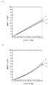
![]()
図3(b)は、この式(101)による、電圧値Vdataの絶対値に対する電流Idの変化を示すグラフである。
That is, Expression (101) does not simply represent the voltage-current characteristics of the transistor T3, but represents characteristics when the pixel driving circuit DC is substantially regarded as one element, and β represents the pixel driving circuit. It is an effective current amplification factor of DC.
![]()
FIG. 3B is a graph showing the change of the current Id with respect to the absolute value of the voltage value Vdata according to the equation (101).
トランジスタT3が初期状態の特性を有していて、閾値電圧Vthが初期の値Vth0を有し、画素駆動回路DCの電流増幅率βが初期の値β0(標準値)を有しているときの特性は、図3(b)に示す電圧−電流特性VI_0で表される。 When the transistor T3 has an initial characteristic, the threshold voltage Vth has an initial value Vth0, and the current amplification factor β of the pixel drive circuit DC has an initial value β0 (standard value). The characteristic is represented by a voltage-current characteristic VI_0 shown in FIG.
ここで、βの標準値としてのβ0は、例えば、画素駆動回路DCの設計値もしくは典型値(Typical値)に設定される。 Here, β0 as a standard value of β is set to, for example, a design value or a typical value (Typical value) of the pixel driving circuit DC.
また、このトランジスタT3が経時劣化して、閾値電圧VthがΔVthだけシフト(増加)したとき、電圧−電流特性は、図3(b)に示す電圧−電流特性VI_3となる。 When the transistor T3 is deteriorated with time and the threshold voltage Vth is shifted (increased) by ΔVth, the voltage-current characteristic becomes the voltage-current characteristic VI_3 shown in FIG.
また、電流増幅率βの値がβ0(標準値)からばらつき、β0より小さいβ1(=β0−Δβ)である場合の電圧−電流特性は電圧−電流特性VI_1になり、β0より大きいβ2(=β0+Δβ)である場合の電圧−電流特性は電圧−電流特性VI_2になる。
Further, the variation from the value [beta] 0 (standard value) of the current amplification factor beta, voltage when a [beta] 0 is smaller than β1 (= β0-Δβ) - current characteristic voltage - become current characteristics VI_ 1, β0 greater than .beta.2 ( = [beta] 0 + [Delta] [beta]) the voltage in the case where - current characteristic voltage - become
このオートゼロ法について説明する。オートゼロ法は、基本的には、まず、上記の書き込み動作において、アノードラインLaの電圧ELVSSに対する電位差の絶対値が閾値電圧Vthを超える基準電圧VrefをデータラインLdiから画素21(i,j)の画素駆動回路DCトランジスタT3のゲート−ソース間に印加する。 The auto zero method will be described. In the auto-zero method, first, in the above write operation, the reference voltage Vref in which the absolute value of the potential difference with respect to the voltage ELVSS of the anode line La exceeds the threshold voltage Vth is applied to the pixel 21 (i, j) from the data line Ldi. Applied between the gate and source of the pixel drive circuit DC transistor T3.
そして、その後、データラインLdiをハイインピーダンス状態とする。これによってゲートデータラインLd1の電圧を自然緩和(低下)させる。そして、自然緩和が終了した後のデータラインLdiの電圧を測定して、測定した電圧を閾値電圧Vthとする手法である。 Thereafter, the data line Ldi is brought into a high impedance state. This naturally relaxes (decreases) the voltage of the gate data line Ld1. Then, the voltage of the data line Ldi after the natural relaxation is finished is measured, and the measured voltage is set as the threshold voltage Vth.
しかるに、本実施形態におけるオートゼロ法を用いたデータラインLdiの電圧の測定は、上記の自然緩和が完全に終了するより前のタイミングで電圧の測定を行うものである。詳しくは後述する。 However, the measurement of the voltage of the data line Ldi using the auto-zero method in the present embodiment is to measure the voltage at a timing before the natural relaxation is completely completed. Details will be described later.
図4は、本実施形態におけるオートゼロ法を用いたデータラインの電圧の測定方法を説明するための図である。図4(a)は、上記基準電圧Vrefを印加した後、データラインLdiをハイインピーダンス状態にしてからの、データラインLdiの電圧の時間的変化(緩和特性)を示す図である。 FIG. 4 is a diagram for explaining a method of measuring the voltage of the data line using the auto-zero method in the present embodiment. FIG. 4A is a diagram showing a temporal change (relaxation characteristic) of the voltage of the data line Ldi after the data line Ldi is brought into a high impedance state after the reference voltage Vref is applied.
データラインLdiの電圧はデータドライバ22によってゲート電圧Vgs(測定電圧Vmeas(t))として取得される。
The voltage of the data line Ldi is acquired by the
図4(b)は、図3(b)に示したβのバラツキがあるときの、データラインの電圧(測定電圧Vmeas(t))に対する影響を説明するための図である。なお、図4(a)、図4(b)において、縦軸はデータラインLdiの電圧(測定電圧Vmeas(t))の絶対値を示し、横軸は時間tを示し、基準電圧Vrefを印加した後、データラインLdiをハイインピーダンス状態にしたときをt=0として、そこからの経過時間(緩和時間)を示す。 FIG. 4B is a diagram for explaining the influence on the data line voltage (measured voltage Vmeas (t)) when there is a variation of β shown in FIG. In FIGS. 4A and 4B, the vertical axis indicates the absolute value of the voltage (measurement voltage Vmeas (t)) of the data line Ldi, the horizontal axis indicates time t, and the reference voltage Vref is applied. After that, the time when the data line Ldi is set to the high impedance state is set to t = 0, and the elapsed time (relaxation time) therefrom is shown.
オートゼロ法によるデータラインの電圧の測定について、更に詳しく説明する。書き込み動作状態において、まず、トランジスタT3の閾値電圧Vthを超える電圧値を有する基準電圧VrefをデータラインLdiから画素21(i,j)の画素駆動回路DCトランジスタT3のゲート−ソース間に印加すると、アノード回路12からアノードラインLa、トランジスタT3、トランジスタT2を介して、データラインLdiに向けて基準電圧Vrefに対応した電流が流れる。
The measurement of the data line voltage by the auto-zero method will be described in more detail. In the write operation state, first, when a reference voltage Vref having a voltage value exceeding the threshold voltage Vth of the transistor T3 is applied between the gate and the source of the pixel drive circuit DC transistor T3 of the pixel 21 (i, j) from the data line Ldi, A current corresponding to the reference voltage Vref flows from the
そして、トランジスタT3のゲート−ソース間(図3(a)の接点N11−N12間)に接続されたストレージ容量Csは基準電圧Vrefに基づく電圧に充電される。なお、基準電圧Vrefは電源電圧ELVSSに対して負極性に設定されている。 The storage capacitor Cs connected between the gate and source of the transistor T3 (between the contacts N11 and N12 in FIG. 3A) is charged to a voltage based on the reference voltage Vref. The reference voltage Vref is set to have a negative polarity with respect to the power supply voltage ELVSS.
次いで、データラインLdiのデータ入力側(データドライバ22側)をハイインピーダンス(HZ)状態に設定する。ハイインピーダンス状態に設定した直後においては、ストレージ容量Csに充電された電圧は基準電圧Vrefに基づく電圧に保持され、トランジスタT3のゲート−ソース間電圧はストレージ容量Csに充電された電圧に保持される。
Next, the data input side (
これにより、ハイインピーダンス状態に設定した直後においてはトランジスタT3はオン状態を維持して、トランジスタT3のドレイン−ソース間に電流が流れ続ける。 As a result, immediately after the high impedance state is set, the transistor T3 maintains the on state, and current continues to flow between the drain and source of the transistor T3.
これにより、トランジスタT3のソース端子側(接点N12)の電位が、時間の経過とともに、ドレイン端子側の電位に近づくように徐々に上昇していき、トランジスタT3のドレイン−ソース間に流れる電流の電流値が減少していく。 As a result, the potential on the source terminal side (contact N12) of the transistor T3 gradually increases so as to approach the potential on the drain terminal side over time, and the current flowing between the drain and source of the transistor T3. The value decreases.
これに伴って、ストレージ容量Csに蓄積された電荷の一部が放電されていく。ストレージ容量Csに蓄積された電荷が徐々に放電されていくと、ストレージ容量Csの両端間の電圧が徐々に減少していく。 Along with this, a part of the electric charge accumulated in the storage capacitor Cs is discharged. As the charge accumulated in the storage capacitor Cs is gradually discharged, the voltage across the storage capacitor Cs gradually decreases.
これによりトランジスタT3のゲート電圧Vgsが徐々に低下していく。これに応じて、図4(a)に示すように、データラインLdiの電圧の絶対値も徐々に低下していく。 As a result, the gate voltage Vgs of the transistor T3 gradually decreases. In response to this, as shown in FIG. 4A, the absolute value of the voltage of the data line Ldi gradually decreases.
そして、最終的に、トランジスタT3のドレイン−ソース間に電流が流れなくなると、ストレージ容量Csに蓄積された電荷の放電が停止する。このときのトランジスタT3のゲート電圧Vgsは、このトランジスタT3の閾値電圧Vthになる。 Finally, when no current flows between the drain and source of the transistor T3, the discharge of the charge accumulated in the storage capacitor Cs stops. At this time, the gate voltage Vgs of the transistor T3 becomes the threshold voltage Vth of the transistor T3.
このときは、トランジスタT2のドレイン−ソース間に電流が流れない状態であるため、トランジスタT2のドレイン−ソース間電圧はほぼゼロになる。このため、このときのデータラインLdiの電圧はトランジスタT3の閾値電圧Vthにほぼ等しくなる。 At this time, since no current flows between the drain and source of the transistor T2, the voltage between the drain and source of the transistor T2 becomes substantially zero. For this reason, the voltage of the data line Ldi at this time is substantially equal to the threshold voltage Vth of the transistor T3.
しかしながら、図4(a)に示すように、データラインLdiの電圧はこの閾値電圧Vthに時間(緩和時間)とともに漸近していく。しかし、この電圧は閾値電圧Vthに限りなく近づくものの、理論的には、緩和時間をいくら長くしても、閾値電圧Vthに完全には等しくならないものである。 However, as shown in FIG. 4A, the voltage of the data line Ldi gradually approaches the threshold voltage Vth with time (relaxation time). However, although this voltage approaches the threshold voltage Vth as much as possible, theoretically, no matter how long the relaxation time is increased, it is not completely equal to the threshold voltage Vth.
そこで、本実施形態においては、表示装置1における制御部16は、ハイインピーダンス状態に設定してからの緩和時間tを予め設定しておく。そして、この設定された緩和時間tにおけるデータラインLdiの電圧(測定電圧Vmeas(t))を測定し、この測定電圧Vmeas(t)に基づいてトランジスタT3の閾値電圧Vth及び画素駆動回路DCの電流増幅率βを取得する。
Therefore, in the present embodiment, the
この測定電圧Vmeas(t)は、次の式(102)によって表される。
ここで、C=Cp+Cs+Celである。
This measured voltage Vmeas (t) is expressed by the following equation (102).
Here, C = Cp + Cs + Cel.
そして、緩和時間tを(C/β)/t<1(すなわち、(C/β)<t)の条件を満たす値に設定すると、その設定された緩和時間tでの測定電圧Vmeas(t)は、次の式(103)によって表される。
ここで、図4(b)に示す緩和時間txを、(C/β)/t=1の条件を満たす時間として、この緩和時間txを超える時間が(C/β)/t<1の条件を満たす緩和時間となる。この緩和時間txは、測定電圧Vmeas(t)が基準電圧Vrefの概ね30%程度になる時間であり、具体的には、概ね1ms〜4ms程度の時間である。 Here, assuming that the relaxation time tx shown in FIG. 4B satisfies the condition of (C / β) / t = 1, the time exceeding the relaxation time tx is (C / β) / t <1. It becomes relaxation time that satisfies. This relaxation time tx is a time during which the measured voltage Vmeas (t) is approximately 30% of the reference voltage Vref, and specifically is a time of approximately 1 ms to 4 ms.
尚、次に、図4(b)に示すVmeas_0(t)は、電流増幅率βが初期の値β0(標準値)である場合(図3(a),(b)に示す電圧−電流特性VI_0に対応)のデータラインLdiの電圧の緩和特性を示す。 Next, Vmeas_0 (t) shown in FIG. 4B is the voltage-current characteristic shown in FIGS. 3A and 3B when the current amplification factor β is the initial value β0 (standard value). The voltage relaxation characteristic of the data line Ldi of VI_0) is shown.
また、図4(b)に示すVmeas_2(t)、Vmeas_3(t)は、それぞれ、電流増幅率βの値がβ0より小さいβ1(=β0−Δβ)である場合と、β0より大きいβ2(=β0+Δβ)である場合(図3(b)に示す電圧−電流特性VI_1,VI_2に対応)のデータラインLdiの電圧の緩和特性を示す。
Also, Vmeas_2 (t) and Vmeas_3 (t) shown in FIG. 4B are respectively obtained when β1 (= β0−Δβ) where the current amplification factor β is smaller than β0 and β2 (= [beta] 0 + If a [Delta] [beta]) voltage shown in (FIG. 3 (b) - current
表示装置1の出荷時等の初期段階で、上記の(C/β)/t<1の条件を満たす緩和時間として、緩和時間txを超える2つの異なる時間=t1,t2を設定して、上記オートゼロ法により、基準電圧Vrefを印加した後の緩和時間t1,t2の2回のタイミングでデータラインLdiの電圧の測定を行う。そして、緩和時間t1及びt2でのデータラインLdiの電圧値と上記の式(103)に基づいて、初期の閾値電圧Vth0と(C/β)とを求めることができる。
At an initial stage such as when the
次いで、上記の手法によって有機ELパネル21の全ての画素21(i,j)に対する閾値電圧Vth0と(C/β)とを求める。そして、各画素21の(C/β)の平均値(<C/β>)と、そのバラツキを計算する。
Next, the threshold voltage Vth0 and (C / β) for all the pixels 21 (i, j) of the
そして、このバラツキが閾値電圧Vth測定の許容精度内に入り、かつ、(C/β)/(βt)<1を満たす最短の緩和時間t=t0を決定する。そして、画像データが供給される実使用時に測定電圧Vmeas(t0)を取得すれば、実使用時の閾値電圧Vthを、式(103)を変形した次の式(104)から求めることができる。 Then, the shortest relaxation time t = t0 that satisfies this variation within the allowable accuracy of the threshold voltage Vth measurement and satisfies (C / β) / (βt) <1 is determined. Then, if the measurement voltage Vmeas (t0) is acquired at the actual use when the image data is supplied, the threshold voltage Vth at the actual use can be obtained from the following equation (104) obtained by modifying the equation (103).
なお、各画素21の(C/β)の平均値(<C/β>)としては、各画素21の(C/β)の加算平均値を用いることができるが、各画素21の(C/β)の値の中央値を用いてもよい。
As the average value of (C / β) of each pixel 21 (<C / β>) , it can be used average value of (C / β) of each
ここで、オフセット電圧を次の式(105)に示すように定義する。
![]()
![]()
次に、画素21(i,j)の画素駆動回路DCの電流増幅率βがβ0±Δβ=β0(1±Δβ/β0)にばらついていた場合について説明する。このときのデータラインLdiの電圧(測定電圧Vmeas(t))のΔβによる変化量ΔVmeas(t)は、次の式(106)によって表される。
(Δβ/β0)は、各画素21(i,j)の画素駆動回路DCの電流特性のバラツキを示すバラツキパラメータであり、ΔVmeas(t)は、データラインLdiの電圧のβのバラツキ依存性を表している。この場合、この式(106)に示すように、βのバラツキによってデータラインLdiの電圧はΔVmeas(t)だけ変動する。 (Δβ / β 0 ) is a variation parameter indicating variation in current characteristics of the pixel drive circuit DC of each pixel 21 (i, j), and ΔVmeas (t) is variation dependency of β on the voltage of the data line Ldi. Represents. In this case, as shown in the equation (106), the voltage of the data line Ldi varies by ΔVmeas (t) due to the variation of β.
このときの緩和時間tは、図4(b)に示すように、緩和時間txに比べて小さな値t3に設定される((C/β)/t≧1)。 As shown in FIG. 4B, the relaxation time t at this time is set to a value t3 that is smaller than the relaxation time tx ((C / β) / t ≧ 1).
この緩和時間t3では、データラインLdiの電圧が急速に緩和(低下)し、データラインLdiの電圧(測定電圧Vmeas(t))のβのバラツキ依存性が比較的大きくなっている。 During the relaxation time t3, the voltage of the data line Ldi is rapidly relaxed (decreased), and the dependence of β on the data line Ldi voltage (measurement voltage Vmeas (t)) is relatively large.
このため、ΔVmeas(t3)で示すように、このΔβに応じた測定電圧Vmeas(t)の変化を判別できる。従って、式(106)に示すΔmeas(t)は、t=t1,t2とした場合と比較して、より大きな値として取得される。 Therefore, as shown by ΔVmeas (t3), the change in the measured voltage Vmeas (t) corresponding to this Δβ can be determined. Therefore, Δmeas (t) shown in Expression (106) is acquired as a larger value compared to the case where t = t1 and t2.
そして、このΔVmeas(t)を取得できれば、式(106)を変形した式から(Δβ/β)を取得できる。 If ΔVmeas (t) can be obtained, (Δβ / β) can be obtained from an equation obtained by modifying equation (106).
次に、供給される画像データに基づいてデータラインLd1に印加される電圧信号の電圧値Vdataに対する補正について説明する。 Next, correction of the voltage value Vdata of the voltage signal applied to the data line Ld1 based on the supplied image data will be described.
まず、画像データに対応する、補正する前の電圧値をVdata0とし、式(106)を電圧で微分することにより、電圧値Vdata0を補正した電圧値Vdata1は次の式(107)で表される。
最後に、閾値電圧Vthは、式(105)で定義したオフセット電圧Voffsetを用い、緩和時間t0におけるオートゼロ法により、次の式(108)で表される。
Vth=Vmeas(t0)−Voffset ・・・(108)
Finally, the threshold voltage Vth is expressed by the following equation (108) by the auto-zero method at the relaxation time t0 using the offset voltage Voffset defined by the equation (105).
Vth = Vmeas (t0) −Voffset (108)
そして、補正した電圧値(補正電圧信号)Vdataは、次の式(109)によって表される。この電圧値Vdataがデータドライバ22からデータラインLd1に印加される電圧信号(駆動信号)の電圧値となる。
Vdata=Vdata1+Vth ・・・(109)
The corrected voltage value (corrected voltage signal) Vdata is expressed by the following equation (109). This voltage value Vdata becomes the voltage value of the voltage signal (drive signal) applied from the
Vdata = Vdata1 + Vth (109)
次に、データドライバ22の構成の詳細について説明する。図5は、図1に示すデータドライバ22の具体的な構成を示すブロック図である。データドライバ22は、図5に示すように、シフトレジスタ111と、データレジスタブロック112と、バッファ113(1)〜113(m),119(1)〜119(m)と、ADC114(1)〜114(m)と、レベルシフタ(図中、「LS」と記す。)115(1)〜115(m),117(1)〜117(m)と、データラッチ部(図中、「D-Latch」と記す。)116(1)〜116(m)と、VDAC118(1)〜118(m)と、スイッチSw1(1)〜Sw1(m),Sw2(1)〜Sw2(m),Sw3(1)〜Sw3(m),Sw4(1)〜Sw4(m),Sw5(1)〜Sw5(m)と、を備える。Sw3(1)〜Sw3(m)は、切換部に相当するものである。
Next, details of the configuration of the
シフトレジスタ111は、制御部16からスタートパルスSP2が供給され、供給されたスタートパルスSP2をシフトして、シフト信号を順次、データレジスタブロック112に供給するものである。
The shift register 111 is supplied with the start pulse SP2 from the
データレジスタブロック112は、m個のレジスタ(図示せず)によって構成されたものである。データレジスタブロック112は、制御部16から画像データに対応するデジタルデータDin(i)(i=1〜m)が供給され、シフトレジスタ111から供給されたシフト信号に従って、これらのデジタルデータDin(i)を、順次、シフトして各レジスタに保持する。
The data register
バッファ113(i)(i=1〜m)は、それぞれ、データラインLdi(i=1〜m)の電圧をアナログデータとしてADC114(i)に印加するためのバッファ回路である。 The buffers 113 (i) (i = 1 to m) are buffer circuits for applying the voltage of the data line Ldi (i = 1 to m) to the ADC 114 (i) as analog data, respectively.
ADC114(i)は、アナログ−デジタル変換器であり、それぞれ、バッファ113(i)から印加されたアナログデータをデジタルデータの出力信号Dout(i)に変換する。ADC114(i)は、データラインLdi(i=1〜m)の電圧を測定する測定器(電圧測定部)として用いられる。 The ADC 114 (i) is an analog-digital converter, and converts the analog data applied from the buffer 113 (i) into an output signal Dout (i) of digital data. The ADC 114 (i) is used as a measuring instrument (voltage measuring unit) that measures the voltage of the data line Ldi (i = 1 to m).
レベルシフタ115(i)は、それぞれ、ADC114(i)が変換したデジタルデータを回路の電源電圧に合わせるようにレベルシフトするものである。 The level shifter 115 (i) shifts the level of the digital data converted by the ADC 114 (i) so as to match the power supply voltage of the circuit.
データラッチ部116(i)は、それぞれ、供給されたデータ信号を保持するためのものである。データラッチ部116(i)は、制御部16から供給されたデータラッチパルスDLpulseの立ち上がりタイミングでデータ信号をラッチする。
Each of the data latch units 116 (i) is for holding a supplied data signal. The data latch unit 116 (i) latches the data signal at the rising timing of the data latch pulse DLpulse supplied from the
レベルシフタ117(i)は、それぞれ、データラッチ部116(i)が保持したデータを回路の電源電圧に合わせるようにレベルシフトするものである。 The level shifter 117 (i) shifts the data held by the data latch unit 116 (i) so as to match the power supply voltage of the circuit.
VDAC(DAC;Digital Analog Converter)118(i)は、デジタルデータをアナログ電圧に変換するデジタル−アナログ変換器である。VDAC118(i)は、レベルシフタ117(i)がレベルシフトしたデジタルデータDin(i)をアナログ電圧に変換して、バッファ119(i)を介して各データラインLdiに出力するものであり、駆動信号印加部に相当する。 A VDAC (DAC: Digital Analog Converter) 118 (i) is a digital-analog converter that converts digital data into an analog voltage. The VDAC 118 (i) converts the digital data Din (i) level-shifted by the level shifter 117 (i) into an analog voltage and outputs the analog voltage to each data line Ldi via the buffer 119 (i). It corresponds to the application unit.
図6は、図5に示すVDAC118の構成と機能を説明するための図である。図6(a)に示すように、VDAC118(i)は、階調電圧生成回路118−1と、階調電圧選択回路118−2と、を有する。
FIG. 6 is a diagram for explaining the configuration and functions of the
階調電圧生成回路118−1は、VDAC118に入力されるデジタル信号のビット数に対応した数の階調電圧(アナログ電圧)を生成するものである。入力されるデジタル信号が図6(a)に示す10ビット(D0−D9)の場合、階調電圧生成回路118−1は、1024個の階調電圧VD0〜VD1023を生成する。
The gradation voltage generation circuit 118-1 generates a number of gradation voltages (analog voltages) corresponding to the number of bits of the digital signal input to the
階調電圧生成回路118−1は、VD1設定回路118−3と、VD1023設定回路118−4と、抵抗R2と、ラダー抵抗部118−5と、を有する。 The gradation voltage generation circuit 118-1 includes a VD1 setting circuit 118-3, a VD1023 setting circuit 118-4, a resistor R2, and a ladder resistor unit 118-5.
VD1設定回路118−3は、制御部16から制御信号VL_SELが供給され、電圧VD0が印加されて、階調電圧VD1の電圧値を設定する回路である。電圧VD0は、最低階調電圧であり、例えば電源電圧ELVSSと同じ電圧に設定される。
The VD1 setting circuit 118-3 is a circuit that is supplied with the control signal VL_SEL from the
VD1設定回路118−3は、図6(b)に示すように、抵抗R3と、複数の抵抗R4−1〜R4−127と、VD1選択回路118−6と、を有する。 As illustrated in FIG. 6B, the VD1 setting circuit 118-3 includes a resistor R3, a plurality of resistors R4-1 to R4-127, and a VD1 selection circuit 118-6.
抵抗R3と抵抗R4−1〜R4−127とは直列接続された分圧抵抗である。抵抗R3の一端には、電圧VD0が印加される。抵抗R4−127の一端は、抵抗R2の一端に接続される。この抵抗R3と抵抗R4−1との接続点の電圧を電圧VA0、・・・、抵抗R4−127と抵抗R2との接続点の電圧を電圧VA127とする。 The resistor R3 and the resistors R4-1 to R4-127 are voltage dividing resistors connected in series. A voltage VD0 is applied to one end of the resistor R3. One end of the resistor R4-127 is connected to one end of the resistor R2. A voltage at a connection point between the resistor R3 and the resistor R4-1 is a voltage VA0,..., And a voltage at a connection point between the resistor R4-127 and the resistor R2 is a voltage VA127.
VD1選択回路118−6は、制御部16から供給された制御信号VL_SELに基づいて、電圧VA0〜VA127のうちから、いずれかの電圧を選択する回路であり、選択した電圧を階調電圧VD1として出力する。ここで、VD1設定回路118−3は、階調電圧VD1を閾値電圧Vth0に対応する値に設定する。
The VD1 selection circuit 118-6 is a circuit that selects one of the voltages VA0 to VA127 based on the control signal VL_SEL supplied from the
VD1023設定回路118−4は、制御部16から制御信号VH_SELが供給され、電圧DVSSが印加されて最高階調電圧VD1023の電圧値を設定する回路である。
The VD1023 setting circuit 118-4 is a circuit that is supplied with the control signal VH_SEL from the
VD1023設定回路118−4は、図6(b)に示すように、複数の抵抗R5−1〜R5−127と、抵抗R6と、VD1023選択回路118−7と、を有する。 As shown in FIG. 6B, the VD1023 setting circuit 118-4 includes a plurality of resistors R5-1 to R5-127, a resistor R6, and a VD1023 selection circuit 118-7.
抵抗R5−1〜R5−127と抵抗R6とは直列接続された分圧抵抗である。抵抗R5−1の一端は、抵抗R2の他端に接続され、抵抗R6の一端には、電圧DVSSが印加される。この抵抗R2と抵抗R5−1との接続点の電圧を電圧VB0、・・・、抵抗R5−127と抵抗R6との接続点の電圧を電圧VB127とする。 The resistors R5-1 to R5-127 and the resistor R6 are voltage dividing resistors connected in series. One end of the resistor R5-1 is connected to the other end of the resistor R2, and the voltage DVSS is applied to one end of the resistor R6. A voltage at a connection point between the resistor R2 and the resistor R5-1 is a voltage VB0,..., And a voltage at a connection point between the resistor R5-127 and the resistor R6 is a voltage VB127.
VD1023選択回路118−7は、制御部16から供給された制御信号VH_SELに基づいて、電圧VB0〜VB127のうちから、いずれかの電圧を選択し、選択した電圧を階調電圧VD1023として出力する回路である。
The VD1023 selection circuit 118-7 selects one of the voltages VB0 to VB127 based on the control signal VH_SEL supplied from the
ラダー抵抗部118−5は、直列に接続された複数(例えば、1022個)のラダー抵抗R1−1〜R1−1022を備えたものであり、各ラダー抵抗R1−1〜R1−1022は、同じ抵抗値を有している。 The ladder resistor unit 118-5 includes a plurality (for example, 1022) of ladder resistors R1-1 to R1-1022 connected in series, and the ladder resistors R1-1 to R1-1022 are the same. It has a resistance value.
ラダー抵抗R1−1の一端は、VD1設定回路118−3の出力端に接続されて電圧VD1が印加される。ラダー抵抗R1−1022の一端は、VD1023設定回路118−4の出力端に接続されて、電圧VD1023が印加される。 One end of the ladder resistor R1-1 is connected to the output end of the VD1 setting circuit 118-3, and the voltage VD1 is applied thereto. One end of the ladder resistor R1-11022 is connected to the output terminal of the VD1023 setting circuit 118-4, and the voltage VD1023 is applied thereto.
そして、ラダー抵抗R1−1〜R1−1022は、電圧VD1〜VD1023を均等に分割し、ラダー抵抗部118−5は、均等に分割した電圧を、等間隔の階調電圧VD2〜VD1022として階調電圧選択回路118−2に出力する。 The ladder resistors R1-1 to R1-1022 equally divide the voltages VD1 to VD1023, and the ladder resistor 118-5 uses the equally divided voltages as gradation voltages VD2 to VD1022 at equal intervals. The voltage is output to the voltage selection circuit 118-2.
階調電圧選択回路118−2は、レベルシフタ117(i)がレベルシフトしたデジタル信号をデジタル信号D0〜D9として入力され、階調電圧生成回路118−1から供給された各階調電圧VD2〜VD1022を、入力されたデジタル信号D0〜D9の値に応じて選択し、選択した階調電圧をVDAC118の出力電圧VOUTとして出力するものである。
The gradation voltage selection circuit 118-2 receives the gradation signals VD2 to VD1022 supplied from the gradation voltage generation circuit 118-1 by inputting the digital signal level-shifted by the level shifter 117 (i) as the digital signals D0 to D9. The selected grayscale voltage is selected as the output voltage VOUT of the
このようにして、VDAC118(i)は、入力されたデジタル信号を、デジタル信号の階調値に対応したアナログ電圧に変換する。 In this way, the VDAC 118 (i) converts the input digital signal into an analog voltage corresponding to the gradation value of the digital signal.
本実施形態においては、VDAC118に入力されるデジタル信号の値は、画像データのビット数に応じた全階調範囲より狭い範囲に設定され、VDAC118(i)が出力する出力電圧VOUTの電圧範囲は、階調電圧生成回路118−1によって生成する全階調電圧VD0〜VD1023のうちの一部の電圧範囲に設定されている。
In the present embodiment, the value of the digital signal input to the
そして、上述のように、本実施形態においては、供給された画像データに対して、概略、閾値電圧Vthの値に応じた補正を行う。すなわち、出力電圧VOUTの電圧範囲の幅は変わらず、第1階調に対応する電圧範囲の開始電圧の値が閾値電圧Vthの変動量(ΔVth)に応じた値だけシフトされて、全階調電圧VD0〜VD1023のうちの電圧範囲がシフトする。 As described above, in this embodiment, the supplied image data is roughly corrected according to the value of the threshold voltage Vth. That is, the width of the voltage range of the output voltage VOUT does not change, and the value of the start voltage in the voltage range corresponding to the first gradation is shifted by a value corresponding to the variation amount (ΔVth) of the threshold voltage Vth, so that all gradations The voltage range of the voltages VD0 to VD1023 is shifted.
しかるに、階調電圧生成回路118−1によって設定される各階調電圧VD1〜VD1023は等間隔の値に設定されているため、出力電圧VOUTの電圧範囲がシフトしても、画像データの階調値に対するVDAC118(i)の出力電圧の変化特性を一定に維持することができる。 However, since the gradation voltages VD1 to VD1023 set by the gradation voltage generation circuit 118-1 are set at equal intervals, even if the voltage range of the output voltage VOUT is shifted, the gradation value of the image data The change characteristic of the output voltage of the VDAC 118 (i) with respect to can be kept constant.
なお、画像データの階調値がゼロであるとき、VDAC118(i)はゼロ階調に対応する最低階調電圧VD0を出力する。このときは黒表示であって有機EL素子101を発光させないため、上記の閾値電圧Vthの値に応じた補正を行う必要がないため、階調電圧VD0は一定の電圧値に設定される。
When the gradation value of the image data is zero, the VDAC 118 (i) outputs the lowest gradation voltage VD0 corresponding to the zero gradation. At this time, since the display is black and the
図5に示すADC114(i)とVDAC118(i)とは、例えば同一のビット幅を有して、1階調に対応する電圧幅が同一の値に設定されている。 The ADC 114 (i) and VDAC 118 (i) shown in FIG. 5 have, for example, the same bit width, and the voltage width corresponding to one gradation is set to the same value.
バッファ119(i)は、それぞれ、VDAC118(i)から出力されたアナログ電圧をデータラインLdiに出力するためのバッファ回路である。 Each of the buffers 119 (i) is a buffer circuit for outputting the analog voltage output from the VDAC 118 (i) to the data line Ldi.
スイッチSw1(i)は、それぞれ、データラインLdiとバッファ119(i)の出力端との間を接続、遮断するスイッチである。 The switch Sw1 (i) is a switch that connects and disconnects between the data line Ldi and the output terminal of the buffer 119 (i).
データラインLdiに電圧値Vdataを有する電圧信号を印加するとき、スイッチSw1(i)は、それぞれ、制御部16から、スイッチ制御信号S1としてOn1信号が供給されてオンし(閉じ)、バッファ119(i)の出力端とデータラインLdiとを接続する。
When a voltage signal having a voltage value Vdata is applied to the data line Ldi, the switch Sw1 (i) is turned on (closed) by being supplied with the On1 signal as the switch control signal S1 from the
データラインLdiへの電圧値Vdataの電圧信号の印加が終了すると、スイッチSw1(i)は、それぞれ、制御部16から、スイッチ制御信号S1としてOff1信号が供給されてオフし(開き)、バッファ119(i)の出力端とデータラインLdiとの間を遮断する。
When the application of the voltage signal of the voltage value Vdata to the data line Ldi is finished, the switch Sw1 (i) is turned off (opened) by supplying the Off1 signal as the switch control signal S1 from the
スイッチSw2(i)は、それぞれ、データラインLdiとバッファ113(i)の入力端との間を接続、遮断するスイッチである。 The switch Sw2 (i) is a switch that connects and disconnects between the data line Ldi and the input end of the buffer 113 (i).
オートゼロ法によるデータラインLdiの電圧測定を行うとき、スイッチSw2(i)は、それぞれ、制御部16から、スイッチ制御信号S2としてOn2信号が供給されてオンし、データラインLdiとバッファ113(i)の入力端との間を接続する。
When the voltage of the data line Ldi is measured by the auto-zero method, the switch Sw2 (i) is turned on when the On2 signal is supplied as the switch control signal S2 from the
データラインLdiの電圧測定が終了すると、スイッチSw2(i)は、それぞれ、制御部16から、スイッチ制御信号S2としてOff2信号が供給されてオフし、データラインLdiとバッファ113(i)の出力端との間を遮断する。
When the voltage measurement of the data line Ldi is completed, the switch Sw2 (i) is turned off by being supplied with the Off2 signal as the switch control signal S2 from the
スイッチSw3(i)は、それぞれ、データラインLdiとアナログ電源14の基準電圧Vrefの出力端との間を接続、遮断するスイッチである。
The switch Sw3 (i) is a switch that connects and disconnects between the data line Ldi and the output terminal of the reference voltage Vref of the
データラインLdiに基準電圧Vrefを印加するとき、スイッチSw3(i)は、それぞれ、制御部16から、スイッチ制御信号S3としてOn3信号が供給されてオンし、アナログ電源14の基準電圧Vrefの出力端とデータラインLdiとを接続する。
When the reference voltage Vref is applied to the data line Ldi, the switch Sw3 (i) is turned on when the On3 signal is supplied as the switch control signal S3 from the
On3信号は上記のオートゼロ法による測定を行うために、基準電圧Vrefを印加する短期間にのみ供給される。その後、スイッチSw3(i)は、それぞれ、制御部16から、スイッチ制御信号S3としてOff3信号が供給されて各スイッチSw3(i)はオフし、アナログ電源14の基準電圧Vrefの出力端とデータラインLdiとの間を遮断する。
The On3 signal is supplied only for a short period of time when the reference voltage Vref is applied in order to perform the measurement by the auto-zero method. After that, the switch Sw3 (i) is supplied with an Off3 signal as the switch control signal S3 from the
スイッチSw4(1)は、データラッチ部116(1)の出力端と、スイッチSw6の一端又はレベルシフタ117(1)との接続切り換えを行うスイッチであり、front端子とDAC側端子とを有している。front端子は、スイッチSw6の一端に接続された端子であり、DAC側端子は、レベルシフタ117(1)に接続された端子である。 The switch Sw4 (1) is a switch for switching connection between the output end of the data latch unit 116 (1) and one end of the switch Sw6 or the level shifter 117 (1), and has a front terminal and a DAC side terminal. Yes. The front terminal is a terminal connected to one end of the switch Sw6, and the DAC side terminal is a terminal connected to the level shifter 117 (1).
また、スイッチSw4(i)(i=2〜m)は、それぞれ、データラッチ部116(i)の出力端と、スイッチSw5(i−1)の入力端又はレベルシフタ117(i)と、の接続切り換えを行うスイッチであり、front端子とDAC側端子とを有している。 Further, the switch Sw4 (i) (i = 2 to m) is a connection between the output end of the data latch unit 116 (i) and the input end of the switch Sw5 (i-1) or the level shifter 117 (i). A switch for switching, and has a front terminal and a DAC side terminal.
スイッチSw4(2)〜(m)のfront端子は、それぞれ、スイッチSw5(1)〜(m−1)と接続するための端子であり、DAC側端子は、それぞれ、レベルシフタ117(2)〜117(m)に接続された端子である。 The front terminals of the switches Sw4 (2) to (m) are terminals for connection to the switches Sw5 (1) to (m-1), respectively, and the DAC side terminals are level shifters 117 (2) to 117, respectively. It is a terminal connected to (m).
測定電圧Vmeas(t)を、出力信号Dout(1)〜Dout(m)として、制御部16に出力するとき、スイッチSw4(i)(i=1〜m)は、制御部16から、それぞれ、スイッチ制御信号S4としてConnect_front信号が供給される。
When the measurement voltage Vmeas (t) is output to the
スイッチSw4(1)は、制御部16からConnect_front信号が供給されて、データラッチ部116(i)の出力端とfront端子とを接続する。
The switch Sw4 (1) is supplied with a Connect_front signal from the
スイッチSw4(i)(i=2〜m)は、制御部16からConnect_front信号が供給されて、それぞれ、データラッチ部116(i)の出力端とfront端子とを接続する。
The switch Sw4 (i) (i = 2 to m) is supplied with the Connect_front signal from the
また、各データラインLdiへの電圧値Vdataの電圧信号の印加が行われるとき、スイッチSw4(i)(i=1〜m)は、それぞれ、制御部16から、スイッチ制御信号S4としてConnect_DAC信号が供給されて、データラッチ部116(i)の出力端とDAC側端子とを接続する。
Further, when the voltage signal of the voltage value Vdata is applied to each data line Ldi, the switch Sw4 (i) (i = 1 to m) receives the Connect_DAC signal from the
スイッチSw5(i)は、それぞれ、データラッチ部116(i)の入力端と、データレジスタブロック112、レベルシフタ115(i)、及びスイッチSw4(i)のいずれか1つのfront端子と、の間の接続切換を行うスイッチである。
The switch Sw5 (i) is between the input terminal of the data latch unit 116 (i) and any one front terminal of the
スイッチSw5(i)は、制御部16から、スイッチ制御信号S5として、それぞれ、Connect_ADC信号が供給されて、データラッチ部116(i)の入力端と、レベルシフタ115(i)の出力端とを接続する。
The switch Sw5 (i) is supplied with a Connect_ADC signal as the switch control signal S5 from the
スイッチSw5(i)は、制御部16から、スイッチ制御信号S5として、それぞれ、Connect_rear信号が供給されて、データラッチ部116(i)の入力端と、スイッチSw4(i+1)のfront端子とを接続する。
The switch Sw5 (i) is supplied with a Connect_rear signal as the switch control signal S5 from the
スイッチSw5(i)は、制御部16から、スイッチ制御信号S5として、それぞれ、Connect_DRB信号が供給されて、データラッチ部116(i)の入力端と、データレジスタブロック112の出力端と、を接続する。
The switch Sw5 (i) is supplied with a Connect_DRB signal as a switch control signal S5 from the
スイッチSw6は、スイッチSw4(1)のfront端子と、制御部16との間を接続、遮断するスイッチである。
Switch Sw6 is connected to a front terminal of switch Sw4 (1), between the
測定電圧Vmeas(t)を、出力信号Dout(1)〜Dout(m)として、制御部16に出力するとき、スイッチSw6は、制御部16から、スイッチ制御信号S6として、On6信号が供給されてオンし、スイッチSw4(1)のfront端子と制御部16とを接続する。
When the measurement voltage Vmeas (t) is output as the output signals Dout (1) to Dout (m) to the
測定電圧Vmeas(t)をすべて出力すると、スイッチSw6は、制御部16から、スイッチ制御信号S6として、Off6信号が供給されてオフし、スイッチSw4(1)のfront端子と制御部16との間を遮断する。
When all the measured voltages Vmeas (t) are output, the switch Sw6 is supplied with an Off6 signal as a switch control signal S6 from the
図1に戻り、アノード回路12は、アノードラインLaを介して有機ELパネル21に電圧を印加して電流を供給するためのものである。
Returning to FIG. 1, the
アナログ電源14は、データドライバ22に基準電圧Vref,電圧DVSS,VD0を印加するための電源である。
The
基準電圧Vrefは、オートゼロ法によるデータラインLd1の電圧測定の際、各画素21(i,j)から電流を引き込むように、データドライバ22に印加される。基準電圧Vrefは、アノード回路12から印加される電源電圧ELVSSに対して負極性の電圧であり、電源電圧ELVSSに対する電位差の絶対値が各画素21(i,j)のトランジスタT3の閾値電圧Vthよりも絶対値で大きな値に設定される。
The reference voltage Vref is applied to the
アナログ電圧DVSSとVD0とは、バッファ113(i),119(i)、ADC114(i)、VDAC118(i)を駆動するためのアナログ電圧である。アナログ電圧DVSSは、アノード回路12から印加される電源電圧ELVSSに対して負極性の電圧であり、例えば−12V程度に設定される。
The analog voltages DVSS and VD0 are analog voltages for driving the buffers 113 (i), 119 (i), the ADC 114 (i), and the VDAC 118 (i). The analog voltage DVSS is a negative voltage with respect to the power supply voltage ELVSS applied from the
ロジック電源15は、データドライバ22に電圧LVSS,LVDDを印加するための電源である。電圧LVSS,LVDDは、データドライバ22のデータラッチ部116(i)、データレジスタブロック、シフトレジスタを駆動するためのロジック電圧である。尚、各電圧DVSS,VD0,LVSS,LVDDは、例えば、(DVSS−VD0)<(LVSS−LVDD)に設定される。
The
制御部16は、各データを格納し、格納したデータに基づいて各部を制御するものである。なお、上述のように、本実施形態における制御部16は、供給されたデジタル信号の画像データに対して種々の補正を行ったデジタルデータDin(i)をデータドライバ22に供給する構成を有する。制御部16内での演算等の処理はデジタル値に対して行われるものである。
The
制御部16は、例えば、表示装置1の出荷時等の初期段階において、各部を制御して、データドライバ22を介して、オートゼロ法によるデータラインLdiの電圧測定を行い、すべての画素21(i,j)に対応する測定電圧Vmeas(t1),Vmeas(t2),Vmeas(t3)を取得する。
For example, in the initial stage such as when the
そして、制御部16は、式(103)に従って演算を行うことにより、特性パラメータとして、各画素21(i,j)のトランジスタT3の(初期)閾値電圧Vth0,画素駆動回路DCのC/β値を取得し、さらに、平均値<C/β>を取得し、式(105)に従って演算を行うことにより、オフセット電圧Voffsetを取得する。
Then, the
次いで、画像データが供給される実使用時において、制御部16は、各部を制御して、データドライバ22を介して、オートゼロ法によるデータラインLdiの電圧測定を行い、すべての画素21(i,j)に対応する測定電圧Vmeas(t0)を取得する。
Next, at the time of actual use in which image data is supplied, the
制御部16は、供給された画像データの電圧データに対し、RGB毎に画像データの階調値に対するデータ値(電圧振幅)の変換を行って電圧値Vdata0を取得する。
The
カラー表示においては、RGB各々が最高階調であるときに白表示となるようにする必要がある。しかし、画素21(i,j)のRGB各色の有機EL素子101は、通常、供給された電流の電流値に対する発光輝度の特性が異なる。
In color display, it is necessary to make white display when each of RGB has the highest gradation. However, the RGB
このため、画像データの階調値に対してRGB各色の有機EL素子101に供給される電流の電流値を、RGBの各々が最高階調であるときに白表示となる互いに異なる値とするように、制御部16において、RGB毎に画像データの階調値に対する電圧振幅の変換を行う。
For this reason, the current values of the currents supplied to the
制御部16は、すべての画素21(i,j)について、このような電圧振幅の変換を行って電圧値Vdata0を取得する。電圧値Vdata0を取得すると、制御部16は、式(106),(107)に従って演算を行うことにより、(Δβ/β0)に基づいて補正した電圧値Vdata1を取得する。
The
制御部16は、式(108),(109)に従って演算を行い、最終出力電圧として、閾値電圧Vthに基づく電圧値Vdataを取得する。具体的に、制御部16は、閾値電圧Vth相当分のビット加算をすることにより電圧値Vdata1を補正し、電圧値Vdataを取得する。
The
制御部16は、補正後のすべての画素21(i,j)に対応する画像データVdataを、デジタルデータDin(1)〜Din(m)として、1行毎にデータドライバ22に出力する。
The
図7は、図1に示す制御部の構成を示すブロック図であり、図8は、図7に示すメモリの各格納領域を示す図である。制御部16は、上記のような処理を行うため、図7に示すように、CPU121と、メモリ122と、LUT123と、を備える。
FIG. 7 is a block diagram showing the configuration of the control unit shown in FIG. 1, and FIG. 8 is a diagram showing each storage area of the memory shown in FIG. The
CPU(Central Processing Unit)121は、実際に、アノード回路12、セレクトドライバ13、データドライバ22の制御、各種演算を行うものである。
A CPU (Central Processing Unit) 121 actually controls the
メモリ122は、ROM(Read Only Memory)、RAM(Random Access Memory)等によって構成されたものであり、CPU121が実行する各処理プログラムを格納するとともに、処理に必要な各種データを格納する。
The
メモリ122は、各種データを格納する領域として、図8に示すように、画素データ格納領域122aと、<C/β>格納領域122bと、オフセット電圧(Voffset)格納領域122cと、を備える。
As shown in FIG. 8, the
画素データ格納領域122aは、画素21(i,j)毎に、測定電圧Vmeas(t1),Vmeas(t2),Vmeas(t3)、ΔVmeas、閾値電圧Vth0、Vth、C/β、Δβ/β0の各データを格納する領域である。
The pixel
<C/β>格納領域122bは、各画素21(i,j)のC/βの平均値<C/β>を格納する領域である。
The <C / β>
オフセット電圧格納領域122cは、式(105)によって定義されたオフセット電圧Voffsetを格納する領域である。
The offset
LUT(Look Up Table)123は、供給された画像データに対してRGB(R;Red、G;Green、B;Blue)各色毎に電圧振幅の変換を行うためのテーブルであり、予め設定されたものである。 An LUT (Look Up Table) 123 is a table for converting voltage amplitude for each color of RGB (R; Red, G; Green, B; Blue) with respect to supplied image data, and is set in advance. Is.
制御部16は、このLUT123を参照することにより、供給された画像データの電圧データに対し、RGB毎にデータ値(電圧振幅)の変換を行う。
The
次に、図9は、VDAC118(i)を10ビットとしてデータ変換を行う場合のLUT123における画像データの変換特性を示す図であり、図10は、LUT123における画像データ変換特性を説明するための図である。
Next, FIG. 9 is a diagram illustrating conversion characteristics of image data in the
この例では、青(B)>赤(R)>緑(G)の順にデータ値(電圧振幅)が異なっている。まず、図9の横軸は画像データの階調値であり、画像データが10ビットの場合を示す。 In this example, data values (voltage amplitudes) are different in the order of blue (B)> red (R)> green (G). First, the horizontal axis of FIG. 9 represents the gradation value of the image data, and shows the case where the image data is 10 bits.
図9の縦軸はLUT123によって画像データを変換した変換データの階調値を示す。この変換データに基づいてRGBの電圧振幅が設定される。なお、画像データの階調値に対する変換データの階調値の変換特性はLUT123に予め設定されているものである。図9(a)は、画像データの階調値に対して変換データの階調値が直線的(リニア)な関係に設定される場合を示している。
The vertical axis in FIG. 9 indicates the gradation value of the converted data obtained by converting the image data by the
また、図9(b)は、画像データの階調値に対して変換データの階調値が曲線的な、ガンマ特性を有するように設定されている場合を示している。LUT123における画像データの階調値に対する変換データの階調値の関係は、必要に応じて任意に設定することができる。
FIG. 9B shows a case where the gradation value of the conversion data is set to have a curved gamma characteristic with respect to the gradation value of the image data. The relationship between the gradation value of the conversion data and the gradation value of the image data in the
ここで、データドライバ22のVDAC118(i)は、10ビットの構成を有している場合、0〜1023の入力データを受けることができるものである。しかし、LUT123によって変換した後の変換データは、最大値が600程度に設定されている。これは以下の理由によるものである。
Here, when the VDAC 118 (i) of the
図10は、画像データの階調値に対する、データドライバ22へ入力されるデジタルデータDin(i)、すなわち、制御部16から出力されるデジタルデータDin(i)の階調値を示したものである。
FIG. 10 shows the gradation value of the digital data Din (i) input to the
ここで、図10(a)は図9(a)に対応し、図10(b)は図9(b)に対応するものである。上述のように、本実施形態においては、制御部16において、供給された画像データに対して、概略、閾値電圧Vthの値に応じた補正を行う。
Here, FIG. 10 (a) corresponds to FIG. 9 (a), and FIG. 10 (b) corresponds to FIG. 9 (b). As described above, in the present embodiment, the
この補正は、式(109)に示すように、画像データに対応し、電流増幅率βのバラツキに応じた補正を行ったデータに対して、閾値電圧Vthに相当する量を加算することによって行われるものである。 As shown in Expression (109), this correction is performed by adding an amount corresponding to the threshold voltage Vth to the data corresponding to the image data and corrected according to the variation in the current amplification factor β. It is what is said.
ここで、上記のように、データドライバ22のVDAC118における階調電圧VD1は閾値電圧Vthの初期値Vth0に対応する値に設定されるため、補正によって加算する量は、閾値電圧Vthの初期値Vth0からの変化量ΔVthに相当する量となる。
Here, as described above, since the gradation voltage VD1 in the
そして、制御部16から出力されるデジタルデータDin(i)の階調値がデータドライバ22のVDAC118(i)の入力可能範囲(0〜1023)内になければならない。
The gradation value of the digital data Din (i) output from the
このために、LUT123によって変換した後の変換データの階調値の最大値は、データドライバ22のVDAC118(i)の入力可能範囲から、補正によって加算される量を減じた値に設定されている。
For this reason, the maximum value of the gradation value of the converted data after conversion by the
なお、補正によって加算される量は閾値電圧Vthの変化量ΔVthに対応したものであるから一定の量ではなく、使用時間の経過に応じて次第に増加するものである。 Note that the amount added by the correction corresponds to the change amount ΔVth of the threshold voltage Vth, and is not a constant amount but gradually increases as the usage time elapses.
よって、LUT123による変換データの階調値の最大値は、例えば、表示装置1の予想される使用時間に基づいて補正によって加算される量の最大値を予測して、決定される。
Therefore, the maximum value of the gradation value of the conversion data by the
なお、画像データの階調値がゼロで黒表示であるときは、有機EL素子101を発光させない状態であるため、上記の補正を行う必要がない。このため、黒表示の画像データがゼロ階調である場合、制御部16は、LUT123を参照することなく、そのままゼロ階調をデータドライバ22に供給する。
Note that when the gradation value of the image data is zero and black display is performed, the
次に本実施形態に係る表示装置1の動作を説明する。
初期段階において、オートゼロ法による各データラインLdiの電圧測定を行う場合、制御部16は、電圧ELVSSをアノードラインLaに印加するように、アノード回路12を制御する。
Next, the operation of the
In the initial stage, when measuring the voltage of each data line Ldi by the auto-zero method, the
図11は、オートゼロ法による電圧測定を行う場合の各部の動作を示すタイミングチャートである。制御部16は、図11に示すように、時刻t10において、セレクトドライバ13に、スタートパルスSP1を供給する。セレクトドライバ13は、セレクトラインLs1に、VgHレベルのGate(1)信号を出力する。
FIG. 11 is a timing chart showing the operation of each part when performing voltage measurement by the auto-zero method. As shown in FIG. 11, the
セレクトドライバ13がセレクトラインLs1にVgHレベルのGate(1)信号を出力すると、第1行目の画素11(i,j)のトランジスタT1,T2はオンする。トランジスタT1がオンすると、トランジスタT3のゲート−ドレイン間が接続されてトランジスタT3は、ダイオード接続状態となる。
When the
また、制御部16は、時刻t10において、データドライバ22に、スイッチ制御信号S1〜S6として、それぞれ、Off1,Off2,On3,Connect_front,Connect_ADC,Off6の各信号を供給する。
Further, at time t10, the
スイッチSw4(1)は、図12(a)に示すように、制御部16からConnect_front信号が供給されて、データラッチ部116(1)の出力端とfront端子とを接続し、スイッチSw4(2)〜Sw4(m)は、それぞれ、データラッチ部116(i)の出力端とfront端子とを接続する。
As shown in FIG. 12A, the switch Sw4 (1) is supplied with the Connect_front signal from the
スイッチSw5(1)〜Sw5(m)は、図12(a)に示すように、制御部16からConnect_ADC信号が供給されて、それぞれ、データラッチ部116(1)〜116(m)の入力端と、レベルシフタ115(1)〜115(m)の出力端とを接続する。
As shown in FIG. 12A, the switches Sw5 (1) to Sw5 (m) are supplied with a Connect_ADC signal from the
図13は、オートゼロ法による電圧測定を行う場合の各スイッチの接続関係を示す図である。スイッチSw1(1)〜Sw1(m),Sw2(1)〜Sw2(m)は、それぞれ、制御部16からOff1,Off2信号が供給されてオフする。また、スイッチSw3(1)〜Sw3(m)は、それぞれ、制御部16からOn3信号が供給されてオンする。
FIG. 13 is a diagram showing the connection relationship of each switch when performing voltage measurement by the auto-zero method. The switches Sw1 (1) to Sw1 (m) and Sw2 (1) to Sw2 (m) are turned off when supplied with Off1 and Off2 signals from the
アナログ電源14の基準電圧Vrefが負であるため、トランジスタT1〜T3がオンすれば、アナログ電源14は、第1行目の画素21(1,1)〜21(1,m)から各データラインLdiを介して電流Idを引き込む。
Since the reference voltage Vref of the
このとき、第1行目の画素21(1,1)〜21(m,1)の有機EL素子101はカソード側の電位がVcathであり、アノード側はVcathより負電位になって逆バイアスとなっているため、電流は流れず、発光しない。
At this time, the
また、スイッチSw1(1)〜Sw1(m),Sw2(1)〜Sw2(m)がオフしているため、アナログ電源14が引き込んだ電流Idは、バッファ113(1)〜113(m),119(1)〜119(m)には流れ込まない。
In addition, since the switches Sw1 (1) to Sw1 (m) and Sw2 (1) to Sw2 (m) are off, the current Id drawn by the
このため、電流Idは、図13(a)に示すように、第1行目の画素21(1,j)〜21(m,j)のトランジスタT3,T2から各データラインLdiを経由してアナログ電源14へと流れる。
For this reason, as shown in FIG. 13A, the current Id flows from the transistors T3 and T2 of the pixels 21 (1, j) to 21 (m, j) in the first row via the data lines Ldi. It flows to the
電流Idが流れると、各画素21(1,j)〜21(m,j)のストレージ容量Csは、基準電圧Vrefに基づく電圧で充電される。 When the current Id flows, the storage capacity Cs of each pixel 21 (1, j) to 21 (m, j) is charged with a voltage based on the reference voltage Vref.
そして、時刻t11において、これらの容量が基準電圧Vrefで充電されると、制御部16は、データドライバ22に、スイッチ制御信号S3としてOff3信号を供給する。
At time t11, when these capacitors are charged with the reference voltage Vref, the
制御部16からOff3信号が供給されると、図13(b)に示すように、それぞれ、スイッチSw3(i)はオフする。また、スイッチSw1(i),Sw2(i)は、それぞれ、オフしたままであり、有機ELパネル21とデータドライバ22との間の接続が遮断される。これにより、データラインLdiはハイインピーダンス(HZ)状態になる。
When the Off3 signal is supplied from the
データラインLdiはハイインピーダンス状態になった直後においては、ストレージ容量Csに蓄積された電荷が直前の値に保持され、これによりトランジスタT3がオン状態に維持される。 Immediately after the data line Ldi enters the high impedance state, the electric charge accumulated in the storage capacitor Cs is held at the previous value, thereby maintaining the transistor T3 in the on state.
これにより、トランジスタT3のドレイン−ソース間に電流が流れ続けて、トランジスタT3のソース端子側の電位がドレイン端子側の電位に近づくように徐々に上昇していき、トランジスタT3のドレイン−ソース間に流れる電流の電流値が減少していく。 As a result, current continues to flow between the drain and source of the transistor T3 and gradually rises so that the potential on the source terminal side of the transistor T3 approaches the potential on the drain terminal side, and between the drain and source of the transistor T3. The current value of the flowing current decreases.
これに伴って、ストレージ容量Csに蓄積された電荷の一部が徐々に放電されていき、ストレージ容量Csの両端間の電圧が減少していく。これによりトランジスタT3のゲート電圧Vgsが徐々に低下していき、これに応じて、データラインLdiの電圧の絶対値は基準電圧Vrefから徐々に低下していく。 Along with this, a part of the electric charge accumulated in the storage capacitor Cs is gradually discharged, and the voltage across the storage capacitor Cs decreases. As a result, the gate voltage Vgs of the transistor T3 gradually decreases, and accordingly, the absolute value of the voltage of the data line Ldi gradually decreases from the reference voltage Vref.
時刻t11から、予め設定された緩和時間tが経過した時刻t12において、制御部16は、データドライバ22に、スイッチ制御信号S2としてOn2信号を供給する。このときの緩和時間tは、C/(βt)<1の条件を満たすt1に設定される。
At time t12 when a preset relaxation time t has elapsed from time t11, the
図13(c)に示すように、スイッチSw2(i)は、それぞれ、制御部16からOn2信号が供給されてオンし、ADC114(i)は、それぞれ、データラインLdiの電圧値を測定電圧Vmeas(t1)としてを取得する。
As shown in FIG. 13C, the switches Sw2 (i) are turned on when the On2 signal is supplied from the
レベルシフタ115(i)は、それぞれ、ADC114(i)が取得した測定電圧Vmeas(t1)をレベルシフトする。 The level shifter 115 (i) shifts the level of the measured voltage Vmeas (t1) acquired by the ADC 114 (i).
図12(a)に示すように、それぞれ、データラッチ部116(1)〜116(m)の入力端と、レベルシフタ115(1)〜115(m)の出力端とがスイッチSw5(1)〜Sw5(m)を介して接続されているため、レベルシフタ115(1)〜115(m)がそれぞれレベルシフトした測定電圧Vmeas(t1)は、データラッチ部116(1)〜116(m)に供給される。 As shown in FIG. 12A, the input terminals of the data latch units 116 (1) to 116 (m) and the output terminals of the level shifters 115 (1) to 115 (m) are connected to the switches Sw5 (1) to Sw5 (1), respectively. Since the level shifters 115 (1) to 115 (m) are level-shifted because they are connected via Sw5 (m), the measured voltages Vmeas (t1) are supplied to the data latch units 116 (1) to 116 (m). Is done.
データラッチ部116(1)〜116(m)は、それぞれ、供給された測定電圧Vmeas(t1)を保持する。制御部16は、データラッチパルスDLpulseをデータドライバ22に出力する。
Each of the data latch units 116 (1) to 116 (m) holds the supplied measurement voltage Vmeas (t1). The
Gate(1)信号が立ち下がる時刻t13において、制御部16は、データドライバ22に、スイッチ制御信号S6として、On6信号を供給し、スイッチSw6は、図12(b)に示すように、オンする。
At time t13 when the Gate (1) signal falls, the
この図12(b)に示すように、データラッチ部116(i)の出力端とスイッチSw6(i)の一端とがスイッチSw4(1)のfront端子を介して接続され、それぞれ、データラッチ部116(2)〜116(m)の出力端と、スイッチSw5(1)〜Sw5(m−1)の入力端と、がスイッチSw4(2)〜Sw4(m)のfront端子を介して接続されている。 As shown in FIG. 12B, the output end of the data latch unit 116 (i) and one end of the switch Sw6 (i) are connected via the front terminal of the switch Sw4 (1). The output ends of 116 (2) to 116 (m) and the input ends of the switches Sw5 (1) to Sw5 (m-1) are connected via the front terminals of the switches Sw4 (2) to Sw4 (m). ing.
このため、データラッチ部116(1)〜116(m)は、制御部16からDLpulseが供給される毎に、保持した第1行目の画素21(1,1)〜21(m,1)に対応するデータラインLdi(i=1〜m)の測定電圧Vmeas(t1)を、順次、転送し、データDout(1)〜Dout(m)として制御部16に出力する。
Therefore, each time the DLpulse is supplied from the
制御部16は、このデータDout(1)〜Dout(m)を取得して、図8に示すメモリ122の画素データ格納領域122aに格納する。このようにして、第1行目の画素21(1,1)〜21(m,1)の電圧測定が終了する。
The
時刻t20において、Gate(2)信号が立ち上がると、制御部16は、同様にして、データドライバ22に、スイッチ制御信号S1〜S6を供給し、第2行目の画素21(1,2)〜21(m,2)に対応するデータラインLdi(i=1〜m)の電圧測定を行う。
When the Gate (2) signal rises at time t20, the
そして、第n行目の画素21(1,n)〜21(m,n)に対応したデータラインLdi(i=1〜m)の電圧測定を行うことにより、時間t1におけるすべての電圧測定が終了する。 Then, by performing voltage measurement on the data line Ldi (i = 1 to m) corresponding to the pixels 21 (1, n) to 21 (m, n) in the nth row, all voltage measurements at time t1 are performed. finish.
次に、制御部16は、同じように、緩和時間tをt2に設定して各画素21(i,j)に対応したデータラインLdiの電圧測定を行う。制御部16は、緩和時間t2における各画素21(i,j)に対応したデータラインLdiの測定電圧Vmeas(t2)を取得し、メモリ122の画素データ格納領域122aに格納する。
Next, similarly, the
次に、制御部16は、同じように、緩和時間tをt3に設定して各画素21(i,j)に対応したデータラインLdiの電圧測定を行う。制御部16は、緩和時間t3における各画素21(i,j)に対応したデータラインLdiの測定電圧Vmeas(t3)を取得し、メモリ122の画素データ格納領域122aに格納する。
Next, similarly, the
図14は、補正パラメータを取得するときに制御部が実行する駆動シーケンスを説明するための図である。制御部16は、測定電圧Vmeas(t1),Vmeas(t2),Vmeas(t3)を取得すると、図14に示す駆動シーケンスに従って演算を行い、補正パラメータを取得する。
FIG. 14 is a diagram for explaining a drive sequence executed by the control unit when acquiring the correction parameter. When acquiring the measurement voltages Vmeas (t1), Vmeas (t2), and Vmeas (t3), the
即ち、制御部16は、メモリ122の各画素データ格納領域122aから、画素21(1,1)に対応したデータラインLdiの測定電圧Vmeas(t1),Vmeas(t2)を読み出す(ステップS11)。
That is, the
そして、制御部16は、式(103)に従って演算を行い、画素21(1,1)に対応した閾値電圧Vth0、C/βを取得する(ステップS12)。
And the
制御部16は、この処理を全画素21(i,j)について行い、全画素21(i,j)に対応した閾値電圧Vth0とC/βとを取得すると、全画素21(i,j)のC/βの平均値<C/β>を取得し(ステップS13)、緩和時間t=t0を決定する。
When the
そして、制御部16は、式(105)によって定義されたオフセット電圧Voffsetを取得する(ステップS14)。
And the
制御部16は、取得した平均値<C/β>、オフセット電圧Voffsetを、それぞれ、メモリ122の<C/β>格納領域122b、オフセット電圧格納領域122cに格納する。
The
制御部16は、メモリ122の各画素データ格納領域122aから、画素21(1,1)の測定電圧Vmeas(t3)を読み出す(ステップS15)。
The
制御部16は、各画素21(i,j)の測定電圧Vmeas(t3)を用い、式(106)を変形して演算を行い、各画素21(i,j)のΔβ/βを取得する(ステップS16)。
The
制御部16は、取得したΔβ/β0を、メモリ122の各画素データ格納領域122aに格納する。
図15は、供給された画像データに応じた電圧信号を補正してデータドライバに出力するときに制御部が実行する駆動シーケンスを説明するための図である。実使用時、制御部16に画像データが供給される。制御部16は、図15に示す駆動シーケンスに従って、画像データに応じた電圧信号の電圧値Vdata0を補正する。
FIG. 15 is a diagram for explaining a drive sequence executed by the control unit when a voltage signal corresponding to supplied image data is corrected and output to the data driver. In actual use, image data is supplied to the
制御部16は、図11に示すタイミングチャートに従って各部を制御し、データドライバ22から、緩和時間t=t0における測定電圧Vmeas(t0)を取得する(ステップS21)。制御部16は、取得した測定電圧Vmeas(t0)をメモリ122の画素データ格納領域122aに格納する。
The
制御部16は、デジタル信号からなる画像データが入力され、画像データに対してLUT123を参照して、RGB毎にデータ値(電圧振幅)を変換して、原階調信号として各画素21(i,j)に対する電圧値Vdata0を生成する(ステップS22)。
The
尚、原階調信号の最大値は、VDAC118(i)の入力範囲における最大値から上述の閾値電圧Vth等の特性パラメータに基づく補正量を減じた値に等しいか、それより小さい値に設定されている。 The maximum value of the original gradation signal is set to a value equal to or smaller than the value obtained by subtracting the correction amount based on the above-described characteristic parameter such as the threshold voltage Vth from the maximum value in the input range of the VDAC 118 (i). ing.
制御部16は、βのバラツキの補正パラメータとして、Δβ/βを用い、式(107)に従って乗算を行い、電圧値Vdata1を取得する(ステップS23)。
The
制御部16は、メモリ122のオフセット電圧格納領域122cから、オフセット電圧Voffsetを読み出し、式(108)に従って測定電圧Vmeas(t0)と負のオフセット電圧Voffsetとを加算し、補正量としての閾値電圧Vthを取得する(ステップS24)。
The
制御部16は、式(109)に従って、電圧値Vdata1と閾値電圧Vthとを加算して、補正階調信号としての電圧値Vdataを取得する(ステップS25)。
The
制御部16は、このような駆動シーケンスを1画素毎に対応して行う。そして、制御部16は、電圧値VdataをデータDin(1)〜Din(m)として、行毎にデータドライバ22に出力する。
The
図16は、実使用時の各部の動作を示すタイミングチャートである。制御部16は、図16に示すデータ出力タイミングチャートに従って各部を制御し、データDin(1)〜Din(m)をデータドライバ22に出力する。
FIG. 16 is a timing chart showing the operation of each unit during actual use. The
制御部16は、時刻t30において、データドライバ22に、スイッチ制御信号S1〜S6として、それぞれ、Off1,Off2,Off3,Connect_DAC,Connect_DRB,Off6信号を供給する。
At time t30, the
図17は、電圧信号を書き込むときの各スイッチの接続関係を示す図である。図17に示すように、Sw2(i),Sw3(i)は、それぞれ、制御部16から、Off2,Off3信号が供給されてオフし、バッファ113(i)とデータラインLdiとの間、アナログ電源14とデータラインLsiとの間が遮断される。
FIG. 17 is a diagram illustrating a connection relationship of each switch when a voltage signal is written. As shown in FIG. 17, Sw2 (i) and Sw3 (i) are turned off when the Off2 and Off3 signals are supplied from the
スイッチSw1(i)は、それぞれ、制御部16から、On1信号が供給されてオンし、バッファ119(i)を介してVDAC118(i)とデータラインLsiとが接続される。
Each of the switches Sw1 (i) is turned on when the On1 signal is supplied from the
図18は、制御部からデータドライバにデータを入力するときの各スイッチの接続関係を示す図である。図18に示すように、スイッチSw5(i)は、それぞれ、制御部16から、Connect_DRB信号が供給されて、データラッチ部116(i)の入力端と、データレジスタブロック112の出力端と、を接続する。
FIG. 18 is a diagram illustrating a connection relationship of each switch when data is input from the control unit to the data driver. As shown in FIG. 18, each of the switches Sw5 (i) is supplied with a Connect_DRB signal from the
スイッチSw4(i)(i=1〜m)は、それぞれ、制御部16から、Connect_DAC信号が供給されて、データラッチ部116(i)の出力端とDAC側端子とを接続する。
Each of the switches Sw4 (i) (i = 1 to m) is supplied with a Connect_DAC signal from the
図5に示すスイッチSw6は、制御部16から、Off6信号が供給されてオフし、データラッチ部116(1)と制御部16との間が遮断される。
The switch Sw6 shown in FIG. 5 is turned off when an Off6 signal is supplied from the
制御部16は、時刻t31において、スタートパルスSP2を立ち上げ、時刻t32において、スタートパルスSP2をLoレベルに立ち下げる。
The
スタートパルスSP2がLoレベルに立ち下がると、データドライバ22のシフトレジスタ111は、クロック信号に従って、このスタートパルスSP2を、順次、シフトし、データレジスタブロック112にシフト信号を供給する。
When the start pulse SP2 falls to the Lo level, the shift register 111 of the
データレジスタブロック112は、このシフト信号が供給されて、順次、データDin(1)〜Din(m)を取り込む。
The data register
時刻t33において、Gate(1)信号がVgHレベルに立ち上がると、画素21(1,1)〜21(m,1)の各トランジスタT1,T2はオンする。 When the Gate (1) signal rises to the VgH level at time t33, the transistors T1 and T2 of the pixels 21 (1,1) to 21 (m, 1) are turned on.
制御部16は、データラッチパルスDLpulseを立ち上げ、データドライバ22のデータラッチ部116(i)は、データラッチパルスDLpulseの立ち上がりタイミングにて、データをラッチする。
The
レベルシフタ117(i)は、それぞれ、データラッチ部116(i)がラッチしたデータに対してレベルシフトを行い、レベルシフトしたデータをVDAC118(i)に供給する。 Each level shifter 117 (i) performs a level shift on the data latched by the data latch unit 116 (i) and supplies the level-shifted data to the VDAC 118 (i).
VDAC118(i)は、このデジタルデータを負のアナログ電圧に変換し、バッファ119(i)を介して、変換した負のアナログ電圧をデータラインLdiに印加する。 The VDAC 118 (i) converts this digital data into a negative analog voltage, and applies the converted negative analog voltage to the data line Ldi via the buffer 119 (i).
データラインLdiに負のアナログ電圧が印加されると、各画素21(1,1)〜21(m,1)の有機EL素子101は逆バイアスとなるために電流は流れず、電流は、アノード回路12から、各画素21(1,1)〜21(m,1)のトランジスタT3,T2、データラインLd1〜Ldmを介して、それぞれ、データドライバ22のVDAC118(i)に流れる。
When a negative analog voltage is applied to the data line Ldi, the
各画素11(1,1)〜21(m,1)の各トランジスタT1はオンしているため、各トランジスタT3は、ゲート−ドレイン間が接続されて、ダイオード接続される。このため、トランジスタT3は、飽和領域内で動作し、トランジスタT3には、ダイオード特性に応じたドレイン電流Idが流れる。 Since each transistor T1 of each pixel 11 (1,1) to 21 (m, 1) is on, each transistor T3 is diode-connected with its gate-drain connected. For this reason, the transistor T3 operates in the saturation region, and a drain current Id corresponding to the diode characteristic flows through the transistor T3.
トランジスタT1がオンし、トランジスタT3にドレイン電流Idが流れるため、トランジスタT3のゲート電圧Vgsは、ドレイン電流Idに対応した電圧に設定され、ストレージ容量Csは、このゲート電圧Vgsで充電される。 Since the transistor T1 is turned on and the drain current Id flows through the transistor T3, the gate voltage Vgs of the transistor T3 is set to a voltage corresponding to the drain current Id, and the storage capacitor Cs is charged with this gate voltage Vgs.
このようにしてデータドライバ22は、補正パラメータに基づいて補正された電流を、図17に示すように、各画素21(1,1)〜21(m,1)のトランジスタT3から引き込んで、ストレージ容量Csに、電圧値Vdataに基づくトランジスタT3のゲート電圧Vgsを保持させる。
In this manner, the
このようにして第1行目の各画素21(1,1)〜21(m,1)のストレージ容量Csへのデータの書き込みが終了する。 In this manner, the writing of data to the storage capacity Cs of each pixel 21 (1,1) to 21 (m, 1) in the first row is completed.
制御部16は、時刻t34になると、DLpulseを立ち下げてスタートパルスSP2を立ち上げ、時刻t35においてスタートパルスSP2を立ち下げて、第2行目の各画素21(1,1)〜21(m,1)のストレージ容量Csへのデータの書き込みを行う。
At time t34, the
以下、同様にして、制御部16は、順次、画素21(1,3)〜21(m,3),・・・,21(1,n)〜21(m,n))のストレージ容量Csに、電圧値Vdataに基づく電圧を書き込む。
Hereinafter, similarly, the
すべての画素21(i,j)のストレージ容量Csに電圧値Vdataの書き込みが行われ、Gate(n)信号がVgLレベルになると、すべての画素21(i,j)のトランジスタT1,T2がオフする。 When the voltage value Vdata is written to the storage capacitors Cs of all the pixels 21 (i, j) and the Gate (n) signal becomes the VgL level, the transistors T1 and T2 of all the pixels 21 (i, j) are turned off. To do.
すべての画素21(i,j)において、それぞれ、トランジスタT1,T2がオフすると、トランジスタT3は、非選択状態となる。トランジスタT3が非選択状態となると、トランジスタT3のゲート電圧Vgsは、ストレージ容量Csに書き込まれた電圧に保持される。 In all the pixels 21 (i, j), when the transistors T1 and T2 are turned off, the transistor T3 is in a non-selected state. When the transistor T3 is in a non-selected state, the gate voltage Vgs of the transistor T3 is held at the voltage written in the storage capacitor Cs.
制御部16は、電圧ELVDDがアノードラインLaに印加されるように、アノード回路12を制御する。この電圧ELVDDは、例えば、15V程度に設定される。
The
このとき、トランジスタT3のゲート電圧Vgsがストレージ容量Csによって保持されているため、トランジスタT3のドレイン−ソース間には、電圧値Vdataを書き込んだときの書き込み電流と同等の電流値のドレイン電流Idが流れる。 At this time, since the gate voltage Vgs of the transistor T3 is held by the storage capacitor Cs, a drain current Id having a current value equivalent to the write current when the voltage value Vdata is written is between the drain and source of the transistor T3. Flowing.
トランジスタT2がオフし、有機EL素子101のアノード側の電位がカソード側の電位より高い状態となっているため、このドレイン電流Idは、有機EL素子101に供給される。
Since the transistor T2 is turned off and the potential on the anode side of the
このとき、各画素21(i,j)の有機EL素子101に流れる電流Idは、閾値電圧Vth,βのバラツキに基づいて補正されており、有機EL素子101は、この補正された電流で発光する。
At this time, the current Id flowing through the
以上説明したように、本実施形態によれば、表示装置1は、緩和時間tとして、(C/β)/t<1を満たす緩和時間t1,t2を選択し、オートゼロ法により、各データラインLdiの電圧測定を複数回行うようにした。
As described above, according to the present embodiment, the
また、表示装置1は、緩和時間tとして、(C/β)/t≧1を満たす時間t3を選択し、オートゼロ法により、各データラインの電圧測定を行うようにして、各画素の画素駆動回路のβのバラツキを示す(Δβ/β0)を取得するようにした。
Further, the
従って、各画素の特性パラメータとして、閾値電圧Vthと(C/β)値と、βのバラツキを示す(Δβ/β0)とを同時に取得することができる。 Therefore, the threshold voltage Vth, the (C / β) value, and (Δβ / β 0 ) indicating the variation of β can be simultaneously acquired as the characteristic parameters of each pixel.
このため、βのバラツキを測定するための回路と閾値電圧Vthを測定のための回路を別々に設ける必要がなくなる。そして、表示装置1の駆動システムを簡素化することができる。また、閾値電圧Vthおよび、画素マトリクスのβのバラツキを補正するアクティブ有機EL駆動システムが可能になる。
Therefore, there is no need to separately provide a circuit for measuring the variation in β and a circuit for measuring the threshold voltage Vth. And the drive system of the
また、実使用時に供給された画像データに基づく電圧信号の電圧値Vdata0を、取得した(Δβ/β)に基づいて補正することができ、さらに、補正された電圧値Vdata1を、取得した閾値電圧Vthと(C/β)値とに基づいて補正し、電圧値Vdataを取得することができる。 Further, the voltage value Vdata0 of the voltage signal based on the image data supplied during actual use can be corrected based on the acquired (Δβ / β), and the corrected voltage value Vdata1 can be corrected using the acquired threshold voltage. Correction is made based on Vth and the (C / β) value, and the voltage value Vdata can be obtained.
このため、実使用時に供給された画像データに基づく電流を各画素21(i,j)の有機EL素子101に供給することができ、画質の劣化を抑制することができる。
For this reason, a current based on the image data supplied during actual use can be supplied to the
尚、本発明を実施するにあたっては、種々の形態が考えられ、上記実施形態に限られるものではない。
例えば、上記実施形態では、発光素子を有機EL素子として説明した。しかし、発光素子は、有機EL素子に限られるものではなく、例えば、無機EL素子又はLEDであってもよい。
In carrying out the present invention, various forms are conceivable and the present invention is not limited to the above embodiment.
For example, in the above embodiment, the light emitting element is described as an organic EL element. However, the light emitting element is not limited to the organic EL element, and may be, for example, an inorganic EL element or an LED.
また、上記実施形態においては、本発明を有機ELパネル21を有する表示装置1に適用した場合について説明したが、本発明はこれに限るものではない。例えば、有機EL素子101による発光素子を有する複数の画素が一方向に配列された、発光素子アレイを備え、感光体ドラムに画像データに応じて発光素子アレイから出射した光を照射して露光する露光装置に適用してもよい。この場合、経時劣化や特性のバラツキによる露光状態の劣化を抑制することができる。
Moreover, in the said embodiment, although the case where this invention was applied to the
上記実施形態では、(C/β)/t<1を満たす緩和時間tとしてt1,t2の2つに設定するようにした。しかし、緩和時間を3つ以上に設定してもよい。 In the above embodiment, the relaxation time t satisfying (C / β) / t <1 is set to t1 and t2. However, the relaxation time may be set to three or more.
上記実施形態では、制御部16が、供給された画像データに応じた電圧信号の電圧値に対して、LUT123を用いて、RGB毎に電圧振幅の変換を行うようにした。しかし、LUT123を備えずに、制御部16は、演算を行うことにより、このような電圧振幅の変換を行うようにしてもよい。
In the embodiment described above, the
1・・・表示装置、11・・・パネルモジュール、12・・・アノード回路、13・・・セレクトドライバ、14・・・アナログ電源、16・・・制御部、21・・・有機ELパネル、21(i,j)(i=1〜m,j=1〜n)・・・画素、22・・・データドライバ、101・・・有機EL素子(発光素子)、114(1)〜114(m)・・・ADC、118(1)〜118(m)・・・VDAC、Sw1(1)〜Sw1(m),Sw2(1)〜Sw2(m),Sw3(1)〜Sw3(m),Sw4(1)〜Sw4(m),Sw5(1)〜Sw5(m),Sw6・・・スイッチ、121・・・CPU、122・・・メモリ、123・・・LUT、T1〜T3・・・トランジスタ、Cs・・・ストレージ容量、Cel・・・有機EL画素容量、Cp・・・配線寄生容量
DESCRIPTION OF
Claims (15)
供給される画像データに応じた駆動信号を、前記各信号線を介して前記各画素に印加する信号線駆動部と、
を備え、
前記信号線駆動部は、
前記各画素の前記駆動素子の閾値電圧を超える電圧値を有する基準電圧を出力する電圧印加部と、
前記各信号線の他端の電圧を測定電圧として取得する電圧測定部と、
前記電圧発生部の出力端と前記各信号線の他端との接続を切り換え、前記信号線の他端と前記電圧印加部を接続して該信号線の他端に前記基準電圧を所定時間印加した後、前記信号線の他端を、前記電圧印加部との接続が遮断された状態に設定する切換部と、
前記切換部により前記信号線の他端が前記電圧印加部との接続が遮断された状態に設定された時点から、予め設定された複数の異なる緩和時間が経過した後に前記電圧測定部により取得される、複数の前記測定電圧の値に基づく特性パラメータを取得する特性パラメータ取得部と、
前記特性パラメータに基づいて、前記画像データに応じた電圧信号の電圧値を補正した補正電圧信号を生成する電圧信号補正部と、
前記補正電圧信号に基づいて前記駆動信号を生成して、前記各信号線の他端に印加する駆動信号印加部と、
を備え、
前記特性パラメータ取得部は、
容量成分C[F]を、前記信号線に寄生する寄生容量と前記保持容量と前記発光素子に寄生する発光素子容量との合計とし、前記画素駆動回路の電流増幅率の設計値をβ0[A/V 2 ]とし、前記緩和時間をt[sec]としたとき、(C/β0)/t<1[V]となる時間で複数の異なる時間[sec]に設定される第1の緩和時間群において、前記電圧測定部により取得される複数の前記測定電圧の値に基づいて、前記各画素の前記駆動素子の第1の閾値電圧と前記画素駆動回路の電流増幅率とを、前記特性パラメータにおける第1の特性パラメータとして算出して取得し、
前記複数の画素における前記容量成分と算出された前記電流増幅率との比率(C/β0)の平均値と、(C/β0)/t≧1[V]となる時間に設定される第2の緩和時間において前記電圧測定部により取得される前記測定電圧の値と、前記各画素の前記第1の閾値電圧の値と、に基づいて、前記電流増幅率の、該電流増幅率の設計値β0に対する偏差をΔβとしたとき、前記偏差Δβの前記電流増幅率の設計値β0に対する比率(Δβ/β0)であるバラツキパラメータを、前記特性パラメータにおける第2の特性パラメータとして算出して取得し、
前記電圧信号補正部は、前記画像データに応じた電圧信号をVdata0、前記補正電圧信号をVdata1、前記バラツキパラメータを(Δβ/β0)としたとき、式(1)に基づいて、前記補正電圧信号を算出する、
ことを特徴とする発光装置。
A signal line drive unit that applies a drive signal corresponding to the supplied image data to each pixel via each signal line;
With
The signal line driver is
A voltage applying unit that outputs a reference voltage having a voltage value exceeding a threshold voltage of the driving element of each pixel;
A voltage measurement unit that obtains the voltage at the other end of each signal line as a measurement voltage;
Switch the connection between the output end of the voltage generator and the other end of each signal line, connect the other end of the signal line and the voltage application unit, and apply the reference voltage to the other end of the signal line for a predetermined time After that, the switching unit for setting the other end of the signal line in a state where the connection with the voltage application unit is cut off,
Acquired by the voltage measurement unit after a plurality of different relaxation times set in advance from the time when the switching unit sets the other end of the signal line to the state where the connection with the voltage application unit is cut off. A characteristic parameter acquisition unit that acquires characteristic parameters based on a plurality of values of the measurement voltage;
A voltage signal correction unit that generates a correction voltage signal obtained by correcting the voltage value of the voltage signal according to the image data based on the characteristic parameter;
A drive signal applying unit that generates the drive signal based on the correction voltage signal and applies the drive signal to the other end of each signal line;
With
The characteristic parameter acquisition unit
The capacitance component C [F] is the sum of the parasitic capacitance parasitic on the signal line, the storage capacitor, and the light emitting element capacitance parasitic on the light emitting element, and the design value of the current amplification factor of the pixel driving circuit is β0 [A / V 2 ], and when the relaxation time is t [sec], the first relaxation time is set to a plurality of different times [sec] with ( C / β0 ) / t <1 [V]. In the group, based on the values of the plurality of measurement voltages acquired by the voltage measurement unit, the first threshold voltage of the driving element of each pixel and the current amplification factor of the pixel driving circuit are set as the characteristic parameter. Calculated and obtained as the first characteristic parameter in
An average value of the ratio (C / β0) between the capacitance component and the calculated current amplification factor in the plurality of pixels, and a second time set as (C / β0) / t ≧ 1 [V] . Based on the value of the measurement voltage acquired by the voltage measurement unit during the relaxation time and the value of the first threshold voltage of each pixel, the design value of the current amplification factor of the current amplification factor When a deviation with respect to β0 is Δβ, a variation parameter that is a ratio (Δβ / β0) of the deviation Δβ to the design value β0 of the current amplification factor is calculated and obtained as a second characteristic parameter ;
When the voltage signal according to the image data is Vdata0, the correction voltage signal is Vdata1, and the variation parameter is (Δβ / β0), the voltage signal correction unit is configured to calculate the correction voltage signal based on Equation (1). To calculate ,
A light emitting device characterized by that.
該画素アレイは、前記第1の方向に直交する第2の方向に沿って配列される複数の走査線を有して、前記複数の画素は前記複数の走査線と前記複数の信号線の各交点近傍に配設され、
前記各走査線に選択信号を順次印加して、各行の前記各画素を順次選択状態に設定する選択駆動部を有し、
前記信号線駆動部の前記特性パラメータ取得部は、前記各信号線を介して、前記選択状態とされた行に対応する前記各画素の前記第1の特性パラメータ及び前記第2の特性パラメータを取得し、
前記駆動信号印加部は、前記選択状態とされた行に対応する前記各画素に、前記各信号線を介して、前記駆動信号を印加する、
ことを特徴とする請求項1に記載の発光装置。 The plurality of signal lines in the pixel array are arranged along a first direction,
The pixel array has a plurality of scanning lines arranged along a second direction orthogonal to the first direction, and the plurality of pixels are each of the plurality of scanning lines and the plurality of signal lines. Arranged near the intersection,
A selection driver that sequentially applies a selection signal to each of the scanning lines and sequentially sets the pixels in each row to a selected state;
The characteristic parameter acquisition unit of the signal line driving unit acquires the first characteristic parameter and the second characteristic parameter of each pixel corresponding to the selected row via each signal line. And
The drive signal applying unit applies the drive signal to the pixels corresponding to the selected row via the signal lines;
The light-emitting device according to claim 1.
電流路の一端に所定の電源電圧が印加され、該電流路の他端に前記発光素子との接続接点が接続された第1の薄膜トランジスタと、
制御端子が前記走査線に接続され、電流路の一端が前記第1の薄膜トランジスタの電流路の一端に接続され、該電流路の他端が前記第1の薄膜トランジスタの制御端子に接続された第2の薄膜トランジスタと、
を備え、
前記駆動素子は、前記第1の薄膜トランジスタであり、
前記選択状態において、前記第2の薄膜トランジスタがオン状態となって、前記第1の薄膜トランジスタの電流路の一端と制御端子とが接続され、
前記選択状態とされた行の前記各画素の前記接続点に、前記電圧印加部より印加される前記基準電圧に応じた電圧が、前記各信号線を介して印加され、
前記電圧測定部は、前記選択状態とされた行の前記各画素の前記接続点の、前記各緩和時間経過後の電圧を、前記各信号線を介して、前記測定電圧として取得する、
ことを特徴とする請求項2に記載の発光装置。 The pixel driving circuit includes at least
A first thin film transistor in which a predetermined power supply voltage is applied to one end of the current path, and a connection contact with the light emitting element is connected to the other end of the current path;
A control terminal is connected to the scanning line, one end of the current path is connected to one end of the current path of the first thin film transistor, and the other end of the current path is connected to the control terminal of the first thin film transistor. A thin film transistor of
With
The drive element is the first thin film transistor;
In the selected state, the second thin film transistor is turned on, and one end of the current path of the first thin film transistor and the control terminal are connected,
A voltage corresponding to the reference voltage applied from the voltage application unit is applied to the connection point of each pixel of the row in the selected state via each signal line,
The voltage measurement unit acquires the voltage after the relaxation time has elapsed as the measurement voltage via the signal lines at the connection point of the pixels in the selected row.
The light-emitting device according to claim 2.
前記電圧信号補正部による前記電圧信号の補正、及び、前記駆動信号印加部による前記駆動信号の生成は、前記画像データが供給されて前記各画素を駆動する実動作時に実行される、
ことを特徴とする請求項1乃至3のいずれか1項に記載の発光装置。 The acquisition of the first characteristic parameter and the second characteristic parameter in the characteristic parameter acquisition unit is executed in an initial state in which the driving element of each pixel has an initial characteristic,
The correction of the voltage signal by the voltage signal correction unit and the generation of the drive signal by the drive signal application unit are performed during an actual operation in which the image data is supplied to drive the pixels.
The light emitting device according to any one of claims 1 to 3 .
ことを特徴とする請求項1乃至4のいずれか1項に記載の発光装置。
The light emitting device according to any one of claims 1 to 4, characterized in that.
ことを特徴とする請求項1に記載の発光装置。
The light-emitting device according to claim 1 .
前記第3の緩和時間に対応する前記測定電圧と前記記憶部に記憶された前記オフセット電圧との差分を、このときの前記各画素の前記第2の閾値電圧とする、
ことを特徴とする請求項7に記載の発光装置。 The drive signal applying unit stores, as an offset voltage, a ratio (<C / β> / t4) between an average value of the ratio between the capacitance component and the current amplification factor in the plurality of pixels and the third relaxation time. A storage unit
The difference between the measured voltage corresponding to the third relaxation time and the offset voltage stored in the storage unit is set as the second threshold voltage of each pixel at this time.
The light-emitting device according to claim 7 .
前記複数の信号線の各々の他端に電圧印加部を接続して、所定の電圧値を有する基準電圧を前記各信号線の他端に印加して、前記各画素の前記駆動素子に、該駆動素子の閾値電圧を超える電圧値を有する基準電圧を印加するステップと、
前記各信号線の他端と前記電圧印加部との接続を遮断した後、複数の異なる緩和時間が経過した後の前記各信号線の他端の電圧を、複数の測定電圧として取得するステップと、
容量成分C[F]を、前記信号線に寄生する寄生容量と前記保持容量と前記発光素子に寄生する発光素子容量との合計とし、前記画素駆動回路の電流増幅率の設計値をβ0[A/V 2 ]とし、前記緩和時間をt[sec]としたとき、(C/β0)/t<1[V]となる時間で複数の異なる時間[sec]に設定される第1の緩和時間において、前記電圧測定部により取得される2つの前記測定電圧の値に基づいて、前記各画素の前記駆動素子の第1の閾値電圧と前記画素駆動回路の電流増幅率とを第1の特性パラメータとして算出して取得するステップと、
前記複数の画素における前記容量成分と算出された前記電流増幅率との比率(C/β)の平均値と、(C/β0)/t≧1[V]となる時間に設定される第2の緩和時間において前記電圧測定部により取得される前記測定電圧の値と、前記各画素の前記第1の閾値電圧の値と、に基づいて、前記電流増幅率の、該電流増幅率の設計値β0に対する偏差をΔβとしたとき、前記偏差Δβの前記電流増幅率の設計値β0に対する比率(Δβ/β0)であるバラツキパラメータを第2の特性パラメータとして算出して取得するステップと、
前記特性パラメータ取得部が取得した前記第2の特性パラメータに基づいて、前記画像データに応じた電圧信号の電圧値を補正した補正電圧信号を生成するステップと、
前記(C/β0)/t<1[V]となる時間に設定される第3の緩和時間において前記電圧測定部により取得される前記測定電圧と、前記容量成分と前記電流増幅率との比率の平均値と、前記補正電圧信号と、に基づいて前記駆動信号を生成して、前記各信号線の他端に印加するステップと、を含む、
前記補正電圧信号を生成するステップは、前記画像データに応じた電圧信号をVdata0、前記補正電圧信号をVdata1、前記バラツキパラメータを(Δβ/β0)としたとき、式(5)に基づいて、前記補正電圧信号を算出するステップを含む、
ことを特徴とする発光装置の駆動制御方法。
A voltage application unit is connected to the other end of each of the plurality of signal lines, a reference voltage having a predetermined voltage value is applied to the other end of each signal line, and the drive element of each pixel has the Applying a reference voltage having a voltage value exceeding a threshold voltage of the driving element;
Obtaining the voltage at the other end of each signal line after a plurality of different relaxation times have passed as a plurality of measurement voltages after disconnecting the connection between the other end of each signal line and the voltage application unit; ,
The capacitance component C [F] is the sum of the parasitic capacitance parasitic on the signal line, the storage capacitor, and the light emitting element capacitance parasitic on the light emitting element, and the design value of the current amplification factor of the pixel driving circuit is β0 [A / V 2 ], and when the relaxation time is t [sec], the first relaxation time is set to a plurality of different times [sec] with ( C / β0 ) / t <1 [V]. In the first characteristic parameter, the first threshold voltage of the driving element of each pixel and the current amplification factor of the pixel driving circuit are set to a first characteristic parameter based on two measurement voltage values acquired by the voltage measuring unit. Calculating and obtaining as:
An average value of the ratio (C / β) between the capacitance component and the calculated current amplification factor in the plurality of pixels, and a second time set as (C / β0) / t ≧ 1 [V] . Based on the value of the measurement voltage acquired by the voltage measurement unit during the relaxation time and the value of the first threshold voltage of each pixel, the design value of the current amplification factor of the current amplification factor calculating and obtaining a variation parameter, which is a ratio (Δβ / β0) of the deviation Δβ to the design value β0 of the current amplification factor as a second characteristic parameter , where Δβ is a deviation from β0 ;
Generating a corrected voltage signal by correcting the voltage value of the voltage signal according to the image data based on the second characteristic parameter acquired by the characteristic parameter acquisition unit;
Ratio of the measurement voltage acquired by the voltage measurement unit in the third relaxation time set to the time when ( C / β0 ) / t <1 [V], and the capacitance component and the current amplification factor Generating the drive signal based on an average value of the correction voltage signal and applying the correction signal to the other end of each signal line.
The step of generating the correction voltage signal is based on the equation (5) when the voltage signal corresponding to the image data is Vdata0, the correction voltage signal is Vdata1, and the variation parameter is (Δβ / β0). Calculating a corrected voltage signal;
A drive control method for a light-emitting device.
前記2つの第1の緩和時間群をt1[sec]、t2[sec]、該第1の緩和時間群に対応する前記測定電圧をVmeas(t1)[V]、Vmeas(t2)[V]、前記第1の閾値電圧をVth1[V]、前記電流増幅率をβ[A/V 2 ]とし、前記2つの測定電圧の値と前記2つの緩和時間の値とを式(6)に代入して演算を行うことにより、前記第1の特性パラメータを算出して取得するステップを含む、
ことを特徴とする請求項10に記載の発光装置の駆動制御方法。
The two first relaxation time groups are t1 [sec] and t2 [sec] , and the measured voltages corresponding to the first relaxation time groups are Vmeas (t1) [V] , Vmeas (t2) [V] , The first threshold voltage is Vth1 [V] , the current amplification factor is β [A / V 2 ], and the two measured voltage values and the two relaxation time values are substituted into equation ( 6 ). Calculating and obtaining the first characteristic parameter by performing calculation
The drive control method of the light-emitting device according to claim 10 .
前記第2の緩和時間をt3[sec]、該第2の緩和時間に対応する前記測定電圧をVmeas(t3)[V]、前記基準電圧の電圧値をVref[V]、前記各画素における前記第1の閾値電圧をVth1[V]、前記複数の画素における前記容量成分と前記電流増幅率との比率の平均値を<C/β>、前記バラツキパラメータをΔβ/β0としたとき、式(7)に基づいて、前記第2の特性パラメータを算出して取得するステップを含む、
ことを特徴とする請求項10又は11に記載の発光装置の駆動制御方法。
The second relaxation time is t3 [sec] , the measurement voltage corresponding to the second relaxation time is Vmeas (t3) [V] , the voltage value of the reference voltage is Vref [V] , and the voltage in each pixel is the first threshold voltage Vth1 [V], the average value of the ratio between the capacitance component and the current amplification factor of the plurality of pixels <C / β>, when the variation parameter was Δβ / β 0, wherein Calculating and obtaining the second characteristic parameter based on ( 7 ),
The drive control method of the light-emitting device according to claim 10 or 11 .
前記第3の緩和時間をt4[sec]、該第3の緩和時間に対応する前記測定電圧をVmeas(t4)[V]、前記複数の画素における前記容量成分と前記電流増幅率との比率の平均値を<C/β>、このときの前記各画素の閾値電圧を第2の閾値電圧Vth2[V]としたとき、式(8)に基づいて、前記第2の閾値電圧を算出するステップを含む、
ことを特徴とする請求項10乃至12のいずれか1項に記載の発光装置の駆動制御方法。
The third relaxation time is t4 [sec] , the measurement voltage corresponding to the third relaxation time is Vmeas (t4) [V] , and the ratio between the capacitance component and the current amplification factor in the plurality of pixels is Step of calculating the second threshold voltage based on the equation (8), where the average value is <C / β> and the threshold voltage of each pixel at this time is the second threshold voltage Vth2 [V] . including,
Drive control method for a light emitting device according to any one of claims 10 to 12, wherein the.
前記複数の画素における前記容量成分と前記電流増幅率との比率の平均値と前記第3の緩和時間との比率(<C/β>/t4)をオフセット電圧として記憶するステップと、
前記第3の緩和時間に対応する前記測定電圧と前記記憶された前記オフセット電圧との差分を、このときの前記各画素の第2の閾値電圧とするステップを含む、
ことを特徴とする請求項10乃至12のいずれか1項に記載の発光装置の駆動制御方法。 The step of generating the drive signal and applying it to the other end of each signal line includes:
Storing an average value of a ratio between the capacitance component and the current amplification factor in the plurality of pixels and a ratio of the third relaxation time (<C / β> / t4) as an offset voltage;
A step of setting a difference between the measured voltage corresponding to the third relaxation time and the stored offset voltage as a second threshold voltage of each pixel at this time,
Drive control method for a light emitting device according to any one of claims 10 to 12, wherein the.
前記補正電圧信号と前記第2の閾値電圧とを加算した信号を前記駆動信号として、前記各信号線の他端に印加するステップを含む、
ことを特徴とする請求項14に記載の発光装置の駆動制御方法。 The step of generating the drive signal and applying it to the other end of each signal line includes:
Applying a signal obtained by adding the correction voltage signal and the second threshold voltage to the other end of each signal line as the drive signal;
The drive control method of the light-emitting device according to claim 14 .
Priority Applications (7)
| Application Number | Priority Date | Filing Date | Title |
|---|---|---|---|
| JP2008305715A JP5012776B2 (en) | 2008-11-28 | 2008-11-28 | Light emitting device and drive control method of light emitting device |
| TW098140534A TWI430224B (en) | 2008-11-28 | 2009-11-27 | A light emitting device and a drive control method in a light emitting device |
| PCT/JP2009/070368 WO2010061973A1 (en) | 2008-11-28 | 2009-11-27 | An electroluminescent light emitting device and drive control method for driving an electroluminescent light emitting device |
| CN2009801095383A CN101978413B (en) | 2008-11-28 | 2009-11-27 | Light emitting device and a drive control method for driving a light emitting device |
| KR1020107023236A KR101206700B1 (en) | 2008-11-28 | 2009-11-27 | A light emitting device and a drive control method for driving a light emitting device |
| US12/626,752 US8279211B2 (en) | 2008-11-28 | 2009-11-27 | Light emitting device and a drive control method for driving a light emitting device |
| HK11108102.5A HK1154106A1 (en) | 2008-11-28 | 2011-08-04 | A light emitting device and drive control method for driving a light emitting device |
Applications Claiming Priority (1)
| Application Number | Priority Date | Filing Date | Title |
|---|---|---|---|
| JP2008305715A JP5012776B2 (en) | 2008-11-28 | 2008-11-28 | Light emitting device and drive control method of light emitting device |
Publications (2)
| Publication Number | Publication Date |
|---|---|
| JP2010128398A JP2010128398A (en) | 2010-06-10 |
| JP5012776B2 true JP5012776B2 (en) | 2012-08-29 |
Family
ID=41683126
Family Applications (1)
| Application Number | Title | Priority Date | Filing Date |
|---|---|---|---|
| JP2008305715A Expired - Fee Related JP5012776B2 (en) | 2008-11-28 | 2008-11-28 | Light emitting device and drive control method of light emitting device |
Country Status (7)
| Country | Link |
|---|---|
| US (1) | US8279211B2 (en) |
| JP (1) | JP5012776B2 (en) |
| KR (1) | KR101206700B1 (en) |
| CN (1) | CN101978413B (en) |
| HK (1) | HK1154106A1 (en) |
| TW (1) | TWI430224B (en) |
| WO (1) | WO2010061973A1 (en) |
Families Citing this family (47)
| Publication number | Priority date | Publication date | Assignee | Title |
|---|---|---|---|---|
| CA2443206A1 (en) | 2003-09-23 | 2005-03-23 | Ignis Innovation Inc. | Amoled display backplanes - pixel driver circuits, array architecture, and external compensation |
| US8576217B2 (en) | 2011-05-20 | 2013-11-05 | Ignis Innovation Inc. | System and methods for extraction of threshold and mobility parameters in AMOLED displays |
| US10013907B2 (en) | 2004-12-15 | 2018-07-03 | Ignis Innovation Inc. | Method and system for programming, calibrating and/or compensating, and driving an LED display |
| US9799246B2 (en) | 2011-05-20 | 2017-10-24 | Ignis Innovation Inc. | System and methods for extraction of threshold and mobility parameters in AMOLED displays |
| KR20080032072A (en) | 2005-06-08 | 2008-04-14 | 이그니스 이노베이션 인크. | Method and system for driving a light emitting device display |
| TW200746022A (en) | 2006-04-19 | 2007-12-16 | Ignis Innovation Inc | Stable driving scheme for active matrix displays |
| CA2556961A1 (en) | 2006-08-15 | 2008-02-15 | Ignis Innovation Inc. | Oled compensation technique based on oled capacitance |
| JP4957710B2 (en) | 2008-11-28 | 2012-06-20 | カシオ計算機株式会社 | Pixel driving device and light emitting device |
| JP5012774B2 (en) * | 2008-11-28 | 2012-08-29 | カシオ計算機株式会社 | Pixel drive device, light emitting device, and parameter acquisition method |
| JP2010185953A (en) * | 2009-02-10 | 2010-08-26 | Fuji Electric Holdings Co Ltd | Driving method and driving circuit of organic el active matrix |
| US9311859B2 (en) | 2009-11-30 | 2016-04-12 | Ignis Innovation Inc. | Resetting cycle for aging compensation in AMOLED displays |
| US9384698B2 (en) | 2009-11-30 | 2016-07-05 | Ignis Innovation Inc. | System and methods for aging compensation in AMOLED displays |
| US10319307B2 (en) | 2009-06-16 | 2019-06-11 | Ignis Innovation Inc. | Display system with compensation techniques and/or shared level resources |
| JP4877536B2 (en) * | 2009-07-10 | 2012-02-15 | カシオ計算機株式会社 | Pixel drive device, light emitting device, drive control method thereof, and electronic apparatus |
| JP2011095720A (en) * | 2009-09-30 | 2011-05-12 | Casio Computer Co Ltd | Light-emitting apparatus, drive control method thereof, and electronic device |
| JP5240581B2 (en) * | 2009-12-28 | 2013-07-17 | カシオ計算機株式会社 | Pixel drive device, light emitting device, drive control method thereof, and electronic apparatus |
| US20140313111A1 (en) | 2010-02-04 | 2014-10-23 | Ignis Innovation Inc. | System and methods for extracting correlation curves for an organic light emitting device |
| US9881532B2 (en) | 2010-02-04 | 2018-01-30 | Ignis Innovation Inc. | System and method for extracting correlation curves for an organic light emitting device |
| CA2692097A1 (en) | 2010-02-04 | 2011-08-04 | Ignis Innovation Inc. | Extracting correlation curves for light emitting device |
| US10089921B2 (en) | 2010-02-04 | 2018-10-02 | Ignis Innovation Inc. | System and methods for extracting correlation curves for an organic light emitting device |
| US8907991B2 (en) | 2010-12-02 | 2014-12-09 | Ignis Innovation Inc. | System and methods for thermal compensation in AMOLED displays |
| US9530349B2 (en) | 2011-05-20 | 2016-12-27 | Ignis Innovations Inc. | Charged-based compensation and parameter extraction in AMOLED displays |
| US9466240B2 (en) | 2011-05-26 | 2016-10-11 | Ignis Innovation Inc. | Adaptive feedback system for compensating for aging pixel areas with enhanced estimation speed |
| US9773439B2 (en) | 2011-05-27 | 2017-09-26 | Ignis Innovation Inc. | Systems and methods for aging compensation in AMOLED displays |
| US9324268B2 (en) | 2013-03-15 | 2016-04-26 | Ignis Innovation Inc. | Amoled displays with multiple readout circuits |
| US10089924B2 (en) | 2011-11-29 | 2018-10-02 | Ignis Innovation Inc. | Structural and low-frequency non-uniformity compensation |
| KR101493226B1 (en) * | 2011-12-26 | 2015-02-17 | 엘지디스플레이 주식회사 | Method and apparatus for measuring characteristic parameter of pixel driving circuit of organic light emitting diode display device |
| US8937632B2 (en) | 2012-02-03 | 2015-01-20 | Ignis Innovation Inc. | Driving system for active-matrix displays |
| US8922544B2 (en) | 2012-05-23 | 2014-12-30 | Ignis Innovation Inc. | Display systems with compensation for line propagation delay |
| KR101992904B1 (en) * | 2012-12-21 | 2019-06-26 | 엘지디스플레이 주식회사 | Organic light emitting diode display device and driving method the same |
| EP2779147B1 (en) | 2013-03-14 | 2016-03-02 | Ignis Innovation Inc. | Re-interpolation with edge detection for extracting an aging pattern for AMOLED displays |
| KR102014852B1 (en) * | 2013-08-30 | 2019-08-27 | 엘지디스플레이 주식회사 | Image Quality Compensation Device And Method Of Organic Light Emitting Display |
| US9761170B2 (en) | 2013-12-06 | 2017-09-12 | Ignis Innovation Inc. | Correction for localized phenomena in an image array |
| KR102101182B1 (en) * | 2013-12-23 | 2020-04-16 | 엘지디스플레이 주식회사 | Organic light emitting display device |
| CN103714780B (en) | 2013-12-24 | 2015-07-15 | 京东方科技集团股份有限公司 | Grid driving circuit, grid driving method, array substrate row driving circuit and display device |
| US9502653B2 (en) | 2013-12-25 | 2016-11-22 | Ignis Innovation Inc. | Electrode contacts |
| CN103730089B (en) * | 2013-12-26 | 2015-11-25 | 京东方科技集团股份有限公司 | Gate driver circuit, method, array base palte horizontal drive circuit and display device |
| CN103714781B (en) | 2013-12-30 | 2016-03-30 | 京东方科技集团股份有限公司 | Gate driver circuit, method, array base palte horizontal drive circuit and display device |
| CA2879462A1 (en) | 2015-01-23 | 2016-07-23 | Ignis Innovation Inc. | Compensation for color variation in emissive devices |
| CA2889870A1 (en) | 2015-05-04 | 2016-11-04 | Ignis Innovation Inc. | Optical feedback system |
| CA2892714A1 (en) | 2015-05-27 | 2016-11-27 | Ignis Innovation Inc | Memory bandwidth reduction in compensation system |
| CA2900170A1 (en) | 2015-08-07 | 2017-02-07 | Gholamreza Chaji | Calibration of pixel based on improved reference values |
| KR102334248B1 (en) * | 2015-10-27 | 2021-12-03 | 삼성디스플레이 주식회사 | Organic light emitting display device |
| WO2018187091A1 (en) * | 2017-04-07 | 2018-10-11 | Apple Inc. | Sensing of pixels with data chosen in consideration of image data |
| US11164515B2 (en) | 2017-04-07 | 2021-11-02 | Apple Inc. | Sensing considering image |
| CN107591126A (en) * | 2017-10-26 | 2018-01-16 | 京东方科技集团股份有限公司 | Control method and its control circuit, the display device of a kind of image element circuit |
| CN110534046B (en) * | 2019-08-30 | 2023-03-10 | 京东方科技集团股份有限公司 | Array substrate, display device and data compensation method |
Family Cites Families (20)
| Publication number | Priority date | Publication date | Assignee | Title |
|---|---|---|---|---|
| JP2002156923A (en) | 2000-11-21 | 2002-05-31 | Sony Corp | Active matrix type display device and active matrix type organic electroluminescence display device |
| JP4266682B2 (en) * | 2002-03-29 | 2009-05-20 | セイコーエプソン株式会社 | Electronic device, driving method of electronic device, electro-optical device, and electronic apparatus |
| JPWO2004100118A1 (en) * | 2003-05-07 | 2006-07-13 | 東芝松下ディスプレイテクノロジー株式会社 | EL display device and driving method thereof |
| JP4048497B2 (en) * | 2003-11-07 | 2008-02-20 | カシオ計算機株式会社 | Display device and drive control method thereof |
| US7907137B2 (en) * | 2005-03-31 | 2011-03-15 | Casio Computer Co., Ltd. | Display drive apparatus, display apparatus and drive control method thereof |
| JP4798342B2 (en) * | 2005-03-31 | 2011-10-19 | カシオ計算機株式会社 | Display drive device and drive control method thereof, and display device and drive control method thereof |
| JP5240534B2 (en) * | 2005-04-20 | 2013-07-17 | カシオ計算機株式会社 | Display device and drive control method thereof |
| JP4940760B2 (en) * | 2006-05-30 | 2012-05-30 | セイコーエプソン株式会社 | Driving transistor characteristic measuring method, electro-optical device, and electronic apparatus |
| JP5240542B2 (en) * | 2006-09-25 | 2013-07-17 | カシオ計算機株式会社 | Display driving device and driving method thereof, and display device and driving method thereof |
| JP4222426B2 (en) * | 2006-09-26 | 2009-02-12 | カシオ計算機株式会社 | Display driving device and driving method thereof, and display device and driving method thereof |
| JP5240538B2 (en) * | 2006-11-15 | 2013-07-17 | カシオ計算機株式会社 | Display driving device and driving method thereof, and display device and driving method thereof |
| JP4470955B2 (en) * | 2007-03-26 | 2010-06-02 | カシオ計算機株式会社 | Display device and driving method thereof |
| JP2008242323A (en) | 2007-03-28 | 2008-10-09 | Sanyo Electric Co Ltd | Light emission display device |
| JP5240544B2 (en) * | 2007-03-30 | 2013-07-17 | カシオ計算機株式会社 | Display device and driving method thereof, display driving device and driving method thereof |
| JP4976926B2 (en) | 2007-06-08 | 2012-07-18 | パナソニック株式会社 | Tabletop |
| JPWO2009110132A1 (en) * | 2008-03-06 | 2011-07-14 | 富士電機株式会社 | Active matrix display device |
| JP5012775B2 (en) | 2008-11-28 | 2012-08-29 | カシオ計算機株式会社 | Pixel drive device, light emitting device, and parameter acquisition method |
| JP4957710B2 (en) | 2008-11-28 | 2012-06-20 | カシオ計算機株式会社 | Pixel driving device and light emitting device |
| JP5012774B2 (en) * | 2008-11-28 | 2012-08-29 | カシオ計算機株式会社 | Pixel drive device, light emitting device, and parameter acquisition method |
| JP4877536B2 (en) * | 2009-07-10 | 2012-02-15 | カシオ計算機株式会社 | Pixel drive device, light emitting device, drive control method thereof, and electronic apparatus |
-
2008
- 2008-11-28 JP JP2008305715A patent/JP5012776B2/en not_active Expired - Fee Related
-
2009
- 2009-11-27 CN CN2009801095383A patent/CN101978413B/en not_active Expired - Fee Related
- 2009-11-27 TW TW098140534A patent/TWI430224B/en not_active IP Right Cessation
- 2009-11-27 US US12/626,752 patent/US8279211B2/en active Active
- 2009-11-27 KR KR1020107023236A patent/KR101206700B1/en active IP Right Grant
- 2009-11-27 WO PCT/JP2009/070368 patent/WO2010061973A1/en active Application Filing
-
2011
- 2011-08-04 HK HK11108102.5A patent/HK1154106A1/en not_active IP Right Cessation
Also Published As
| Publication number | Publication date |
|---|---|
| JP2010128398A (en) | 2010-06-10 |
| US8279211B2 (en) | 2012-10-02 |
| WO2010061973A1 (en) | 2010-06-03 |
| TWI430224B (en) | 2014-03-11 |
| US20100134469A1 (en) | 2010-06-03 |
| HK1154106A1 (en) | 2012-04-13 |
| KR20100127831A (en) | 2010-12-06 |
| CN101978413B (en) | 2013-09-11 |
| KR101206700B1 (en) | 2012-11-30 |
| CN101978413A (en) | 2011-02-16 |
| TW201030709A (en) | 2010-08-16 |
Similar Documents
| Publication | Publication Date | Title |
|---|---|---|
| JP5012776B2 (en) | Light emitting device and drive control method of light emitting device | |
| JP5012775B2 (en) | Pixel drive device, light emitting device, and parameter acquisition method | |
| JP4957710B2 (en) | Pixel driving device and light emitting device | |
| JP5012774B2 (en) | Pixel drive device, light emitting device, and parameter acquisition method | |
| JP5146521B2 (en) | Pixel drive device, light emitting device, drive control method thereof, and electronic apparatus | |
| KR102056784B1 (en) | Organic light emitting display device | |
| TWI446319B (en) | Pixel driving device, light emitting device, driving/controlling method thereof, and electronic device for example digital camera, mobile computer, and mobile phone | |
| US8339384B2 (en) | Display driving apparatus, display apparatus and drive control method for display apparatus | |
| JP4935920B2 (en) | Pixel drive device, light emitting device, drive control method thereof, and electronic apparatus | |
| JP2016021006A (en) | El device, and driving method el device |
Legal Events
| Date | Code | Title | Description |
|---|---|---|---|
| A131 | Notification of reasons for refusal |
Free format text: JAPANESE INTERMEDIATE CODE: A132 Effective date: 20120207 |
|
| A521 | Request for written amendment filed |
Free format text: JAPANESE INTERMEDIATE CODE: A523 Effective date: 20120409 |
|
| TRDD | Decision of grant or rejection written | ||
| A01 | Written decision to grant a patent or to grant a registration (utility model) |
Free format text: JAPANESE INTERMEDIATE CODE: A01 Effective date: 20120508 |
|
| A01 | Written decision to grant a patent or to grant a registration (utility model) |
Free format text: JAPANESE INTERMEDIATE CODE: A01 |
|
| A61 | First payment of annual fees (during grant procedure) |
Free format text: JAPANESE INTERMEDIATE CODE: A61 Effective date: 20120521 |
|
| FPAY | Renewal fee payment (event date is renewal date of database) |
Free format text: PAYMENT UNTIL: 20150615 Year of fee payment: 3 |
|
| R150 | Certificate of patent or registration of utility model |
Ref document number: 5012776 Country of ref document: JP Free format text: JAPANESE INTERMEDIATE CODE: R150 Free format text: JAPANESE INTERMEDIATE CODE: R150 |
|
| S111 | Request for change of ownership or part of ownership |
Free format text: JAPANESE INTERMEDIATE CODE: R313113 |
|
| R350 | Written notification of registration of transfer |
Free format text: JAPANESE INTERMEDIATE CODE: R350 |
|
| R250 | Receipt of annual fees |
Free format text: JAPANESE INTERMEDIATE CODE: R250 |
|
| R250 | Receipt of annual fees |
Free format text: JAPANESE INTERMEDIATE CODE: R250 |
|
| R250 | Receipt of annual fees |
Free format text: JAPANESE INTERMEDIATE CODE: R250 |
|
| LAPS | Cancellation because of no payment of annual fees |