JP5008223B2 - Active matrix display device - Google Patents
Active matrix display device Download PDFInfo
- Publication number
- JP5008223B2 JP5008223B2 JP2001020078A JP2001020078A JP5008223B2 JP 5008223 B2 JP5008223 B2 JP 5008223B2 JP 2001020078 A JP2001020078 A JP 2001020078A JP 2001020078 A JP2001020078 A JP 2001020078A JP 5008223 B2 JP5008223 B2 JP 5008223B2
- Authority
- JP
- Japan
- Prior art keywords
- source signal
- source
- power supply
- line
- conversion circuits
- Prior art date
- Legal status (The legal status is an assumption and is not a legal conclusion. Google has not performed a legal analysis and makes no representation as to the accuracy of the status listed.)
- Expired - Fee Related
Links
Images


Landscapes
- Liquid Crystal Display Device Control (AREA)
- Control Of Indicators Other Than Cathode Ray Tubes (AREA)
- Control Of El Displays (AREA)
- Liquid Crystal (AREA)
Description
【0001】
【発明の属する技術分野】
【0002】
本発明は、マトリクス状に配置されたスイッチング素子と画素により映像などの情報の表示をおこなうカラー画像表示装置(アクティブマトリクス型カラー画像表示装置)、特にデジタル方式の駆動方法およびそれを用いた画像表示装置、電子機器に関する。
【0003】
【従来の技術】
最近安価なガラス基板上に半導体薄膜を形成した半導体装置、例えば薄膜トランジスタ(TFT)を作製する技術が急速に発達してきている。その理由は、アクティブマトリクス型画像表示装置の需要が高まってきたことによる。
【0004】
アクティブマトリクス型画像表示装置には、表示素子に液晶を用いるアクティブマトリクス型液晶表示装置やエレクトロルミネッセンス(EL)素子を用いるEL表示装置などがある。以下では、アクティブマトリクス型画像表示装置の代表的な例として、アクティブマトリクス型液晶表示装置を例にとって説明する。
【0005】
アクティブマトリクス型液晶表示装置は、図30に示すように、ソース信号線駆動回路101と、ゲート信号線駆動回路102と、マトリクス状に配置された画素アレイ部103とを有している。ソース信号線駆動回路101は、クロック信号等のタイミング信号に同期して、入力された映像信号をサンプリングし各ソース信号線104にデータを書き込む。ゲート信号線駆動回路102は、クロック信号等のタイミングに同期して、ゲート信号線105を順次選択し、画素アレイ部103の各画素内にあるスイッチング素子であるTFT(画素TFT)106のオン・オフを制御するようになっている。これにより、各ソース信号線104に書き込まれたデータが順次各画素に書き込まれることになる。
【0006】
ソース信号線駆動回路の駆動方式としては、アナログ方式とデジタル方式があるが、高精細・高速駆動が可能なデジタル方式のアクティブマトリクス型液晶表示装置が注目されてきている。
【0007】
従来のデジタル方式のソース信号線駆動回路を図31に示す。図31において、201はシフトレジスタ部を示し、フリップフロップ回路などを含むシフトレジスタ基本回路202から構成される。シフトレジスタ部201へスタートパルスSPが入力されるとクロック信号CLKに同期してサンプリングパルスが順次ラッチ1回路203(LAT1)へ送出される。
【0008】
ラッチ1回路203(LAT1)では、シフトレジスタ部からのサンプリングパルスに同期して、データバスライン(DATA―R、DATA―G、DATA―B)から供給されるnビット(nは自然数)のデジタル映像信号を順次記憶する。
【0009】
一水平画素分の信号がLAT1部へ書き込まれた後、各ラッチ1回路203(LAT1)に保持されているデジタル映像信号は、ラッチ信号バスライン(LP)から供給されるラッチパルスに同期してラッチ2回路204(LAT2)に一斉に転送される。
【0010】
デジタル映像信号がラッチ2回路204(LAT2)に保持されると、再びスタートパルス(SP)が入力され、次行の画素分のデジタル映像信号がLAT1部へ新たに書き込まれる。この間、LAT2部へは、前行の画素分のデジタル映像信号が記憶されておりデジタル/アナログ信号変換回路(以降、D/A変換回路と記す)205(D/A)によって、デジタル映像信号に対応したアナログ映像信号が各ソース信号線に書き込まれる。図31において、Vref-R、Vref-G、Vref-Bは、それぞれR(赤)、G(緑)、B(青)の各色に対応したD/A変換回路205に接続される階調電源線を示す。また、SL1、SL2、・・・等は番号付けしたソース信号線を、SL1等の下に記したR、G、Bはそれぞれ赤、緑、青を示し、単板でカラー表示可能な表示装置を想定している。
【0011】
図31に示した各D/A変換回路205はそれぞれ1本のソース信号線と接続され、その1本のソース信号線にアナログ映像信号を書き込む。しかし、高解像度、高精細の液晶表示装置を作成する場合、大きな面積を占めるD/A変換回路をソース信号線と同数作ることは近年望まれている液晶表示装置の小型化の妨げとなっており、1つのD/A変換回路で複数のソース信号線を駆動する方法が特開平11−167373で提案されている。
【0012】
1つのD/A変換回路で4本のソース信号線を駆動するソース信号線駆動回路の構成例を図32に示す。図31と比較して判るように図32にはパラレル/シリアル変換回路301(P/S変換回路)、ソース線選択回路302とそれらに入力される選択信号(SS)が新たに追加されている。このような回路が追加されるにもかかわらず、4本のソース信号線に1つのD/A変換回路で信号の書き込みができれば、必要なD/A変換回路数が1/4で済む効果は大きく、ソース信号線駆動回路の占有面積を小さくすることが可能となる。
【0013】
【発明が解決しようとする課題】
図31においては、RGB用に独立な3系統の階調電源線がソース信号線駆動回路に供給されている。しかし、図32に示したソース信号線駆動回路には、図31と異なり1系統の階調電源線のみが供給されている。一般に、階調電源線の電源電圧が与えられれば、D/A変換回路の出力電圧範囲は一意に決まる。従って、1系統の階調電源線が供給されている図32のソース信号線駆動回路は、各ソース信号線に書き込まれる電圧範囲はRGBの区別なく同じになる。
【0014】
さて、液晶表示装置の輝度比の液晶印加電圧依存性は、RGB各色で全く同じというわけではなく、図33に示す例のように色によって異なる。この例では、輝度比が極小値をとる電圧値がRGBそれぞれに対してVR、(<)VG、(<)VBと異なる。従って、液晶に電圧を印加していったときに階調表現の単調性が失われないためには、液晶に印加できる最大電圧はRGBそれぞれに対してVR、VG、VBとなる。しかし、図32のような1系統の階調電源線しか供給されない場合、前述のように液晶に印加できる電圧範囲はRGBの区別なく一様になるので、図33の輝度比―電圧特性を持った液晶に対しては、印加できる最大電圧がVRとなる。この時、GやBが十分に暗の状態にならず、コントラストが低くなるばかりか、正確な色彩の表現性に乏しくなってしまう問題が生じる。
【0015】
以上の理由から、図31に示したように階調電源線もRGB独立に3系統供給するなどして、液晶の印加電圧をRGB独立に制御できるようにすることが望ましい。
【0016】
しかし、上記の3系統の階調電源線を供給する方法で、1つのD/A変換回路で複数のソース信号線を駆動する場合では、階調電源線の本数が増加するばかりか、それら階調電源線の1つとD/A変換回路との接続切り替えをおこなうスイッチが必要になる。これらは、外部入力ピン数の増加や、階調電源線を配線する領域や上記の追加するスイッチ等による駆動回路の占有面積の増加など新たな問題を生じさせる。これでは、1つのD/A変換回路で複数のソース信号線を駆動し、駆動回路の占有面積を減少させるメリットがなくなってしまう。
【0017】
そこで本発明は、これらの問題を解決する駆動方法を提供するものである。
【0018】
【課題を解決するための手段】
ソース信号線駆動回路に供給される階調電源線は1系統のみとし、各D/A変換回路はRGBに対応した3本のソース信号線を単位としてその倍数本のソース信号線に対しアナログ映像信号を書き込む。また、1水平書き込み期間内に階調電源線の電源電圧も変化させる。各ソース線選択回路がRGB各色に対応したソース信号線を選択する期間を同期させ、階調電源線に印加する電源電圧は、Rのソース信号線が選択されている期間にはRに対応した電源電圧を、Gのソース信号線が選択されている期間にはGに対応した電源電圧を、Bのソース信号線が選択されている期間にはBに対応した電源電圧をそれぞれ印加する。
【0019】
こうすることで、外部入力ピン数の増加や、駆動回路の占有面積の増加を招くことなく画素電極の電圧をRGB独立に制御することを可能にする。
【0020】
【発明の実施の形態】
以下、本発明の実施の形態について,図面を参照しながら説明する。
【0021】
[実施形態]
本実施形態では、1系統の階調電源線がソース信号線駆動回路に供給され、各D/A変換回路がそれぞれRGBに対応する3本のソース信号線を駆動する方法について説明する。
【0022】
また、本実施形態では、RGB各色それぞれ(n+1)ビット(nは自然数)のデジタル映像信号入力に対応する場合を例にとって説明する。
【0023】
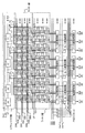
図1には本実施形態の概略回路図が示されている。図1では、デジタル映像信号を順次サンプリングするためのサンプリングパルスを発生させるシフトレジスタ部、前記サンプリングパルスによりデジタル映像信号をラッチするラッチ1回路部、そして、ラッチパルスの入力により前記ラッチ1回路部に記憶されていたデジタル映像信号を一斉にラッチするラッチ2回路部は図示せず省略した。パラレル/シリアル変換回路(P/S変換回路)は、ラッチ2回路のパラレルな出力データ(D0[3k+1]〜Dn[3k+1]、D0[3k+2]〜Dn[3k+2]、D0[3k+3]〜Dn[3k+3](kは0以上の整数))をビット信号毎にまとめシリアルデータに変換する。ここで、D0[3k+1]は第(3k+1)ソース信号線に対する最下位(第1)ビット(LSB)のデジタル映像信号を示し、Dn[3k+1]は同じく第(3k+1)ソース信号線に対する最上位(第(n+1))ビット(MSB)のデジタル映像信号を示す。以降、表記Dl[s]は第sソース信号線に対する第(l+1)ビットのデジタル映像信号を示すものとする。また、第(3k+1)ソース信号線はRを、第(3k+2)ソース信号線はGを、第(3k+3)ソース信号線はBをそれぞれ表示するためのソース信号線とする。
【0024】
ソース線選択回路は3つのスイッチsw1、sw2、sw3から成り、sw1がオンすると第(3k+1)番目のソース信号線(Rを担当するソース信号線)が、sw2がオンすると第(3k+2)番目のソース信号線(Gを担当するソース信号線)が、sw3がオンすると第(3k+3)番目のソース信号線(Bを担当するソース信号線)がそれぞれ各D/A変換回路の出力と接続される。SS1〜SS3はそれぞれsw1〜sw3のオン・オフを制御する選択信号である。
【0025】
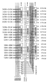
図1の駆動回路に対する信号動作タイミングを図2に示す。1ゲート線選択期間を3つに分割し、第1番目の期間に選択信号SS1をHiレベルにしsw1をオンし、第2番目の期間に選択信号SS2をHiレベルにしsw2をオンし、第3番目の期間に選択信号SS3をHiレベルにしsw3をオンする動作を示す。なお、各P/S変換回路の出力信号(PS0[k]〜PSn[k])は、上記の選択信号(SS1〜SS3)と同期させ、1ゲート線選択期間を3分割した、その第1番目の期間には第(3k+1)ソース信号線に対するデジタル映像信号を出力し、第2番目の期間には第(3k+2)ソース信号線に対するデジタル映像信号を出力し、第3番目の期間には第(3k+3)ソース信号線に対するデジタル映像信号を出力するようにP/S変換回路に入力される選択信号SSにより制御する。こうすることで、各ソース信号線に対応したデジタル映像信号が適切なソース信号線の書き込みに反映される。この様子を、図2のPS0[1]〜PSn[1]、PS0[2]〜PSn[2]に示した。ここでは、PSl[k]は第k段目のP/S変換回路の第(l+1)ビット目の出力信号を示す。従って、PSl[k]は、Dl[3k−2]、Dl[3k−1]、Dl[3k]のデジタル映像信号から構成される。また、図2において、Dl[s、g]は第s列第g行の画素に対する第(l+1)ビット目のデジタル映像信号を示し、表記Dl[s]にあらわにゲート信号線の情報を付加したものである。
【0026】
つぎに、階調電源線Vrefへの電源電圧の入力方法を図2のVrefに示す。図中、Vref-R、Vref-G、Vref-Bは、それぞれR、G、Bの各色に対応した階調電源線の電源電圧を印加することを示す。1ゲート線選択期間を3つに分割した第1番目の期間には、ソース線選択回路により第(3k+1)番目のソース信号線(Rを担当するソース信号線)が選択されているので、Rを表示するための電源電圧が階調電源線に印加される。同様に、1ゲート線選択期間を3つに分割した第2、第3番目の期間にはそれぞれG、Bを表示するための電源電圧がそれぞれ階調電源線に印加される。
【0027】
以上、本実施形態により、1つのD/A変換回路でRGBの3本のソース信号線を駆動する形態において、1系統のみの階調電源線がソース信号線駆動回路に供給された場合であっても、画素電極の電圧をRGB独立に制御することが可能となる。なお、本実施形態では、1つのD/A変換回路でRGBの3本のソース信号線を駆動する場合を例に挙げているが、本発明はこれに限定されるものではなく、3本、6本、・・・といった3の倍数本のソース信号線を1つのD/A変換回路で駆動する場合にも適用され得る。また、ソース線選択回路がソース信号線を選択する順序は、本実施形態のようにR、G、Bの順に限定されるものではなく、他の順序でもよい。さらに、本実施形態では、パラレル/シリアル変換回路(P/S変換回路)を用いたが、本発明はこの有無に限定されない。すなわち、本発明はD/A変換回路に1ゲート線選択期間、複数のソース信号線に対するデジタル映像信号をシリアル入力するいかなる方法に対しても適用され得る。
【0028】
【実施例】
ここで、本発明の実施例について、図面を参照しながら説明する。ただし、本発明は、以下の実施例に限定されるわけではない。
【0029】
[実施例1]
本実施例では、アクティブマトリクス型画像表示装置に本発明を適用した例を示す。アクティブマトリクス型画像表示装置は、従来例で示したようにソース信号線駆動回路、ゲート信号線駆動回路、マトリクス状に配置された画素アレイ部とから構成されている。ゲート信号線駆動回路と画素アレイ部の動作は従来例と同じなので、本実施例ではソース信号線駆動回路について説明する。また、図3に示すように、本実施例では、RGB各色に対するデジタル映像信号は3ビットとし、1つのD/A変換回路でRGBの3本のソース信号線を駆動する場合を例に説明する。
【0030】
シフトレジスタ部は、フリップフロップ回路(FF)、NAND回路、およびインバータ回路を有し、クロック信号(CLK)、前記クロック信号の反転クロック信号(CLKb)およびスタートパルス(SP)が入力される。図4(A)に示すように、フリップフロップ回路(FF)はクロックドインバータ回路、インバータ回路で構成されている。
【0031】
スタートパルス(SP)が入力されると、クロック信号(CLK、CLKb)に同期してサンプリングパルスが順次シフトしていく。
【0032】
記憶回路であるラッチ1部とラッチ2部は、基本ラッチ回路(LAT)から構成されている。基本ラッチ回路を図4(B)に示す。基本ラッチ回路(LAT)はクロックドインバータ回路とインバータ回路で構成されている。ラッチ1部へはR、G、B、各3ビットのデジタル映像信号(DR0、DR1、DR2、DG0、DG1、DG2、DB0、DB1、DB2)が入力され、シフトレジスタ部からのサンプリングパルスによって、デジタル映像信号をラッチする。ラッチ2部は、水平帰線期間に入力されるラッチパルス(LP)によって、ラッチ1部に保持されていたデジタル映像信号を一斉にラッチすると同時に下流の回路に情報を伝達する。この時、ラッチ2部には1水平書き込み期間データが保持される。
【0033】
なお、図4(A)および(B)において、各クロックドインバータ回路のPチャネル型トランジスタへのクロック入力端子の接続が省略されているが、実際はNチャネル型トランジスタへのクロック入力端子に入力されている制御信号の反転信号が入力される。また、本実施例ではフリップフロップ回路(FF)と基本ラッチ回路(LAT)は同じ回路構成をしているが、異なる回路構成であってもよい。
【0034】
パラレル/シリアル変換回路(図3ではP/S変換回路Aとした)へは、3(ビット数)×3(RGBで3本のソース信号線分)のラッチ2部に記憶されているデジタル映像信号と、選択信号(SS1〜SS3)が入力される。図5(A)に示すように、P/S変換回路AはNAND回路から構成されている。
【0035】
図7に、第1〜第3ソース信号線(SL1〜SL3)に関わるP/S変換回路Aに注目した信号動作タイミングを示す。1ゲート線選択期間を3つに分割し、第1番目の期間に選択信号(SS1)をHiレベルにし、第1ソース信号線(SL1)に対するデジタル映像信号をD/A変換回路に出力する。第2番目の期間は、選択信号(SS2)をHiレベルにし、第2ソース信号線(SL2)に対するデジタル映像信号をD/A変換回路に出力する。第3番目の期間は、選択信号(SS3)をHiレベルにし、第3ソース信号線(SL3)に対するデジタル映像信号をD/A変換回路に出力する。この様子を、図7のPS0[1]〜PS2[1]に示した。ここで、PSl[1]は、第1〜第3ソース信号線(SL1〜SL3)に関わるP/S変換回路Aの第(l+1)ビット目の出力データである。また、前述したようにDl[s、g]は第s列第g行の画素に対する第(l+1)ビット目のデジタル映像信号を示している。ここで、RGBで区別したDRl、DGl、DBl(l=0〜2)やDl[s] (l=0〜2)には以下の関係がある。
DRl[s]=Dl[3s−2] (l=0〜2)
DGl[s]=Dl[3s−1] (l=0〜2)
DBl[s]=Dl[3s] (l=0〜2)
また、DRl[s]などの表記にゲート信号線の情報を付加したものをDRl[s、g]などと表記する。
【0036】
上記と同様な動作は他のソース信号線(SL4〜SL6、SL7〜SL9、・・・)に関わるP/S変換回路Aでも並行しておこなわれる。
【0037】
D/A変換回路の回路構成例を図6に示す。図6は抵抗ストリング型のD/A変換回路であり、ある電圧範囲の出力を得るためには2本の階調電源線を供給する必要がある。図6では、これらをVref−L、Vref−Hと示した。これらの階調電源電圧を抵抗で分圧し、3ビットのデジタル映像信号に対応した電圧値を出力する。
【0038】
D/A変換回路の出力は、ソース線選択回路Aを介して適切なソース信号線に接続される。ソース線選択回路Aの回路構成例を図5(B)に示す。ソース線選択回路Aは3つのトランスミッションゲート(スイッチ)からなり、各ゲートへ選択信号(SS1〜SS3)とそれらの反転信号が入力される。図7の信号動作タイミングに従えば、1ゲート線選択期間を3つに分割した、第1番目の期間にはスイッチsw1をオンしRの第1ソース信号線(SL1)へD/A変換回路の出力を書きこむ。第2番目の期間にはスイッチsw2をオンしGの第2ソース信号線(SL2)へD/A変換回路の出力を書きこむ。最後の、第3番目の期間にはスイッチsw3をオンしBの第3ソース信号線(SL3)へD/A変換回路の出力を書きこむ。
【0039】
このような書き込みは他のソース信号線に対しても並行しておこなわれる。そして、各ソース信号線に書き込まれたデータは、ゲート信号線駆動回路と画素TFTとの働きにより順次各画素に書き込まれることになる。
【0040】
本実施例では、2本の階調電源線Vref−L、Vref−Hのうち、Vref−LはRGB各色について同一電圧としてV0とし、Vref−HはRGBについてそれぞれVR、VG、VBとした。1ゲート線選択期間に階調電源線の電源電圧を変化させる様子は図7に示されている。Rのソース信号線がソース線選択回路に選択されている期間は、Rに対応する電源電圧が印加され、Gのソース信号線がソース線選択回路に選択されている期間は、Gに対応する電源電圧が印加され、Bのソース信号線がソース線選択回路に選択されている期間は、Bに対応する電源電圧が印加される。
【0041】
以上の駆動方法により、1つのD/A変換回路で3本のソース信号線を駆動する場合、ソース信号線駆動回路に供給される階調電源線が1系統のみであっても、画素に印加する電圧をRGB独立に制御することができる。
【0042】
なお、本実施例においてソース信号線駆動回路に供給される回路駆動電源は1系統を仮定したが、2系統以上とし必要な部分にレベルシフタ回路を挿入してもよい。また、本実施例では階調電源線Vref−Lの電源電圧はRGBに対して同一としたが、異なっていてもよい。
【0043】
[実施例2]
本実施例でも、実施例1と同様にアクティブマトリクス型画像表示装置に本発明を適用した例を示すが、実施例1と異なり1つのD/A変換回路で6本(RGB×2)のソース信号線を駆動する例を説明する。本実施例でも主にソース信号線駆動回路について説明する。シフトレジスタ部、ラッチ1部、ラッチ2部については実施例1と同じとし、以下ではそれらの説明を省略する。本実施例におけるラッチ2回路より下流の回路構成例を図8に示す。また、本実施例でも、RGB各色に対するデジタル映像信号は3ビットとする。
【0044】
パラレル/シリアル変換回路(図8ではP/S変換回路Bとした)へは、3(ビット数)×6(RGB×2で6本のソース信号線分)のラッチ2部に記憶されているデジタル映像信号と、選択信号(SS1〜SS6)が入力される。図9(A)に示すように、P/S変換回路BはNAND回路から構成されている。
【0045】
図10に、第1〜第6ソース信号線(SL1〜SL6)に関わるP/S変換回路Bに注目した信号動作タイミングを示す。1ゲート線選択期間を6つに分割した、それぞれの期間毎に6つの選択信号SS1、SS4、SS2、SS5、SS3、SS6がこの順序でHiレベルになるように入力される。こうしてP/S変換回路Bは、ソース信号線SL1(R)、SL4(R)、SL2(G)、SL5(G)、SL3(B)、SL6(B)に対応するデジタル映像信号をこの順序でD/A変換回路に出力する。この様子を、図10のPS0[1]〜PS2[1]に示した。ここで、PSl[1]は、第1〜第6ソース信号線(SL1〜SL6)に関わるP/S変換回路Bの第(l+1)ビット目の出力データである。また、前述したようにDl[s、g]は第s列第g行の画素に対する第(l+1)ビット目のデジタル映像信号を示している。ここで、RGBで区別したDRl、DGl、DBl(l=0〜2)やDl[s] (l=0〜2)にも以下の関係が成立する。
DRl[s]=Dl[3s−2] (l=0〜2)
DGl[s]=Dl[3s−1] (l=0〜2)
DBl[s]=Dl[3s] (l=0〜2)
また、DRl[s]などの表記にゲート信号線の情報を付加したものをDRl[s、g]などと表記する。
【0046】
上記と同様な動作は他のソース信号線(SL7〜SL12、SL13〜SL18、・・・)に関わるP/S変換回路Bでも並行しておこなわれる。
【0047】
D/A変換回路は実施例1と同じで図6に示されるものとする。
【0048】
D/A変換回路の出力は、ソース線選択回路Bを介して適切なソース信号線に接続される。ソース線選択回路Bの回路構成例を図9(B)に示す。ソース線選択回路Bは6つのトランスミッションゲート(スイッチ)からなり、各ゲートへ選択信号(SS1〜SS6)とそれらの反転信号が入力される。図10の信号動作タイミングに従えば、1ゲート線選択期間を6つに分割した、その各期間に6つの選択信号SS1、SS4、SS2、SS5、SS3、SS6がこの順序でHiレベルになる。これにより、ソース線選択回路B内のスイッチはsw1、sw4、sw2、sw5、sw3、sw6の順にオンし、ソース信号線SL1(R)、SL4(R)、SL2(G)、SL5(G)、SL3(B)、SL6(B)をこの順序でD/A変換回路と接続し各ソース信号線への書き込みをおこなう。
【0049】
このような書き込みは他のソース信号線に対しても並行しておこなわれる。そして、各ソース信号線に書き込まれたデータは、ゲート信号線駆動回路と画素TFTとの働きにより順次各画素に書き込まれることになる。
【0050】
本実施例でも、2本の階調電源線Vref−L、Vref−Hのうち、Vref−LはRGB各色について同一電圧V0とし、Vref−HはRGBについてそれぞれVR、VG、VBとした。1ゲート線選択期間に階調電源線の電源電圧を変化させる様子は図10に示されている。Rのソース信号線がソース線選択回路に選択されている期間は、Rに対応する電源電圧が印加され、Gのソース信号線がソース線選択回路に選択されている期間は、Gに対応する電源電圧が印加され、Bのソース信号線がソース線選択回路に選択されている期間は、Bに対応する電源電圧が印加される。
【0051】
本実施例のように、1ゲート線選択期間内においては、RGBについて同色のソース信号線は連続的にD/A変換回路と接続させることにより、階調電源線に印加する電源電圧を変化させる周期を長くすることができ、回路動作負担の低減につながる。
【0052】
以上の駆動方法により、1つのD/A変換回路で6本のソース信号線を駆動する場合、ソース信号線駆動回路に供給される階調電源線が1系統のみであっても、画素に印加する電圧をRGB独立に制御することができる。
【0053】
なお、本実施例においてソース信号線駆動回路に供給される回路駆動電源は1系統を仮定したが、2系統以上とし必要な部分にレベルシフタ回路を挿入してもよい。また、本実施例では階調電源線Vref−Lの電源電圧はRGBに対して同一としたが、異なっていてもよい。また、ソース線選択回路のソース信号線を選択する順序は本実施例には限定されない。
【0054】
[実施例3]
本実施例では、実施例1および実施例2をアクティブマトリクス型液晶表示装置に適用した場合の作成方法例として、画素部のスイッチング素子である画素TFTと、画素部の周辺に設けられる駆動回路(ソース信号線駆動回路、ゲート信号線駆動回路等)のTFTを同一基板上に作製する方法について工程に従って詳細に説明する。但し、説明を簡単にするために、駆動回路部としてはその基本構成回路であるCMOS回路を、画素TFT部としてはnチャネル型TFTとを図示することにする。
【0055】
図11において、基板401には、例えばコーニング社の1737ガラス基板に代表される無アルカリガラス基板を用いる。TFTが形成される基板401の表面に、下地膜402をプラズマCVD法やスパッタ法で形成する。下地膜402は、窒化シリコン膜を25〜100nm、ここでは50nmの厚さに、酸化シリコン膜を50〜300nm、ここでは150nmの厚さに形成する。また、下地膜402は、窒化シリコン膜や窒化酸化シリコン膜のみを用いても良い。
【0056】
次に、この下地膜402の上に50nmの厚さの、非晶質シリコン膜をプラズマCVD法で形成する。非晶質シリコン膜は含有水素量にもよるが、好ましくは400〜550℃で数時間加熱して脱水素処理を行い、含有水素量を5atom%以下として、結晶化の工程を行うことが望ましい。また、非晶質シリコン膜をスパッタ法や蒸着法などの他の作製方法で形成しても良いが、膜中に含まれる酸素、窒素などの不純物元素を十分低減させておくことが望ましい。
【0057】
ここで、下地膜と非晶質シリコン膜とはいずれもプラズマCVD法で作製されるものであり、このとき下地膜と非晶質シリコン膜を真空中で連続して形成しても良い。下地膜を形成後、一旦大気雰囲気にさらされない工程にすることにより、表面の汚染を防ぐことが可能となり、作製されるTFTの特性バラツキを低減させることができる。
【0058】
非晶質シリコン膜を結晶化する工程は、公知のレーザー結晶化技術または熱結晶化の技術を用いれば良い。本実施例では、パルス発振型のKrFエキシマレーザー光を線状に集光して非晶質シリコン膜に照射して結晶質シリコン膜を形成する。
【0059】
尚、本実施例では半導体層となる結晶質シリコン膜を、非晶質シリコン膜から形成するが、非晶質シリコン膜の代わりに微結晶シリコン膜を用いても構わないし、直接結晶質シリコン膜を成膜しても良い。
【0060】
こうして形成された結晶質シリコン膜をパターニングして、島状の半導体層403、404、405を形成する。
【0061】
次に、島状の半導体層403、404、405を覆って、酸化シリコンまたは窒化シリコンを主成分とするゲート絶縁膜406を形成する。ゲート絶縁膜406は、プラズマCVD法でN2OとSiH4を原料とした窒化酸化シリコン膜を10〜200nm、好ましくは50〜150nmの厚さで形成すれば良い。ここでは100nmの厚さに形成する。
【0062】
そして、ゲート絶縁膜406の表面に第1のゲート電極となる第1の導電膜407と、第2のゲート電極となる第2の導電膜408とを形成する。第1の導電膜407はSi、Geから選ばれた一種の元素、またはこれらの元素を主成分とする半導体膜で形成すれば良い。また、第1の導電膜407の厚さは5〜50nm、好ましくは10〜30nmとする必要がある。ここでは、20nmの厚さでSi膜を形成する。
【0063】
第1の導電膜407として使用する半導体膜にはn型あるいはp型の導電型を付与する不純物元素が添加されていても良い。この半導体膜の作製法は公知の方法に従えば良く、例えば、減圧CVD法で基板温度を450〜500℃として、ジシラン(Si2H6)を250SCCM、ヘリウム(He)を300SCCM導入して作製することができる。このとき同時に、Si2H6に対してPH3を0.1〜2%混入させてn型の半導体膜を形成しても良い。
【0064】
第2のゲート電極となる第2の導電膜408は、Ti、Ta、W、Moから選ばれた元素、あるいはこれらの元素を主成分とする化合物で形成すれば良い。これはゲート電極の電気抵抗を下げるために考慮されるものであり、例えば、Mo−W化合物を用いても良い。ここでは、Taを使用し、スパッタ法で、200〜1000nm、代表的には400nmの厚さに形成した。(図11(A))
【0065】
次に公知のパターニング技術を使ってレジストマスクを形成し、第2の導電膜408をエッチングして第2のゲート電極を形成する工程を行う。第2の導電膜408はTa膜で形成されているので、ドライエッチング法によりエッチングを行う。ドライエッチングの条件として、Cl2を80SCCM導入して100mTorrで500Wの高周波電力を投入して行う。そして、図11(B)に示すように第2のゲート電極409、410、412、413と、配線411、414を形成する。第2のゲート電極の、チャネル長方向の長さは、CMOS回路を形成する第2のゲート電極409、410で3μmとし、また、画素TFTはマルチゲートの構造となっていて、第2のゲート電極412、413の各々の長さを2μmとした。
【0066】
また、第2の導電膜408はウエットエッチング法で除去することもできる。例えば、Taの場合、フッ酸系のエッチング液で容易に除去することができる。
【0067】
また、画素TFTを構成するnチャネル型TFTのドレイン側に保持容量を設ける構造となっている。このとき、第2の導電膜と同じ材料で保持容量の配線電極414が形成される。
【0068】
次に、n型を付与する第1の不純物元素を添加する工程を行う。この工程は第2の不純物領域を形成するための工程である。ここでは、フォスフィン(PH3)を用いたイオンドープ法を行う。この工程では、ゲート絶縁膜406と第1の導電膜407を通してその下の半導体層403、404、405にリンを添加するために、加速電圧は80keVと高めに設定する。半導体層403、404、405に添加されるリンの濃度は、1×10¹⁶〜1×10¹⁹atoms/cm3の範囲にするのが好ましく、ここでは1×1018atoms/cm3とする。そして、半導体層にリンが添加された領域415、416、417、418、419、420、421、422が形成される。(図11(B))
【0069】
このとき、第1の導電膜407で、第2のゲート電極409、410、411、412、413、414と重ならない領域にもリンが添加される。この領域のリン濃度は特に規定されるものではないが、第1の導電膜の抵抗率を下げる効果が得られる。
【0070】
次に、nチャネル型TFTが形成される領域をレジストマスク423、424で覆って、第1の導電膜407の一部を除去する工程をドライエッチング法で行う。第1の導電膜407はSiであり、ドライエッチングの条件として、CF4を50SCCM、O2を45SCCM導入し、50mTorrで200Wの高周波電力を投入して行う。その結果、レジストマスク或いはゲート電極で覆われた、第1の導電膜の一部である425、426、427、428が残る。
【0071】
そして、pチャネル型TFTが形成される領域に、p型を付与する第3の不純物元素を添加する工程を行う。ここではジボラン(B2H6)を用いてイオンドープ法で添加する。ここでも加速電圧を80keVとして、2×10²⁰atoms/cm3の濃度にボロンを添加する。そして、図11(C)に示すようにボロンが高濃度に添加された第3の不純物領域429、430が形成される。(図11(C))
【0072】
さらに、レジストマスク423、424を完全に除去して、再度レジストマスク431、432、433、434、435、436を形成する。そして、レジストマスク431、434、435、436を用い、第1の導電膜の一部425、428をエッチングし、新たに第1の導電膜の一部437、438、439、440を形成する。(図12(A))
【0073】
レジストマスク431は9μmの長さで、レジストマスク434、435は7μmの長さで形成する。これにより、n型を付与する第1の不純物添加の工程でリンが添加された半導体層のうち、レジストマスク431、434、435で覆われた下の領域が、第2の不純物領域として次の工程の後確定することになる。
【0074】
次に、n型を付与する第2の不純物元素を添加する工程を行う。ここでは、フォスフィン(PH3)を用いたイオンドープ法で行う。この工程でも、ゲート絶縁膜406を通してその下の半導体層にリンを添加するために、加速電圧は80keVと高めに設定する。そして、リンが添加された第1の不純物領域441、442、443、444、445が形成される。この領域のリンの濃度はn型を付与する第1の不純物元素を添加する工程と比較して高濃度であり、1×10¹⁹〜1×10²¹atoms/cm3とするのが好ましく、ここでは1×1020atoms/cm3とする。(図12(A))
【0075】
さらに、レジストマスク431、432、433、434、435、436を除去して新たにレジストマスク446、447、448、449、450、451を形成する。この工程において、nチャネル型TFTに形成されるレジストマスク446、449、450のチャネル長方向の長さはTFTの構造を決める上で重要である。レジストマスク446、449、450は第1の導電膜437、438、439の一部を除去する目的で設けられるものであり、このレジストマスクの長さにより、第2の不純物領域がゲート電極と重なる領域と、重ならない領域をある範囲で自由に決めることができる。(図12(B))
【0076】
そして、レジストマスク446、449、450を使用したエッチングにより、図12(C)に示すように第1のゲート電極452、453、454が形成される。ここで、第1のゲート電極452の、チャネル長方向の長さは6μm、第1のゲート電極453、454のチャネル長方向の長さは4μmとした。
【0077】
また、画素部には、保持容量部の電極455が形成される。
【0078】
図12(C)までの工程が終了したら、窒化シリコン膜456、第1の層間絶縁膜457を形成する工程を行う。最初に窒化シリコン膜456を50nmの厚さに成膜する。窒化シリコン膜456はプラズマCVD法で形成され、SiH4を5SCCM、NH3を40SCCM、N2を100SCCM導入して0.7Torr、300Wの高周波電力を投入する。続いて、第1の層間絶縁膜457として酸化シリコン膜を採用し、TEOSを500SCCM、O2を50SCCM導入し1Torr、200Wの高周波電力を投入して950nmの厚さに成膜する。
【0079】
次に、熱処理の工程を行う。熱処理の工程は、それぞれの濃度で添加されたn型またはp型を付与する不純物元素を活性化するために行う必要がある。この工程は、電気加熱炉を用いた熱アニール法や、前述のエキシマレーザーを用いたレーザーアニール法や、ハロゲンランプを用いたラピットサーマルアニール法(RTA法)で行えば良い。ここでは熱アニール法で活性化の工程を行う。加熱処理は、窒素雰囲気中において300〜700℃、好ましくは350〜550℃、ここでは450℃、2時間の処理を行う。
【0080】
第1の層間絶縁膜457と窒化シリコン膜456には、その後、パターニングでそれぞれのTFTのソース領域と、ドレイン領域に達するコンタクトホール形成のためエッチングされる。そして、ソース電極458、459、460とドレイン電極461、462を形成する。図示していないが、本実施例ではこの電極を、Ti膜を100nm、Tiを含むAl膜300nm、Ti膜150nmをスパッタ法で連続形成した3層構造の電極として用いる。
【0081】
そして、ソース電極458、459、460とドレイン電極461、462と、第1の層間絶縁膜457を覆ってパッシベーション膜463を形成する。パッシベーション膜463は、窒化シリコン膜で50nmの厚さで形成する。さらに、有機樹脂からなる第2の層間絶縁膜464を約1000nmの厚さに形成する。有機樹脂膜としては、ポリイミド、アクリル、ポリイミドアミド等を使用することができる。有機樹脂膜を用いることの利点は、成膜方法が簡単である点や、比誘電率が低いので、寄生容量を低減できる点、平坦性に優れる点などが上げられる。なお上述した以外の有機樹脂膜を用いることもできる。ここでは、基板に塗布後、熱重合するタイプのポリイミドを用い、300℃で焼成して形成する。
【0082】
以上の工程で、CMOS回路のnチャネル型TFTにはチャネル形成領域465、第1の不純物領域468、469、第2の不純物領域466、467が形成される。ここで、第2の不純物領域は、ゲート電極と重なる領域(GOLD領域)466a、467aが1.5μmの長さに、ゲート電極と重ならない領域(LDD領域)466b、467bが1.5μmの長さにそれぞれ形成される。第1の不純物領域468はソース領域、第1の不純物領域469はドレイン領域となる。
【0083】
pチャネル型TFTは、同様にクラッド構造のゲート電極が形成され、チャネル形成領域470、第3の不純物領域471、472が形成される。そして、第3の不純物領域471はソース領域、第3の不純物領域472はドレイン領域となる。
【0084】
また、画素TFTであるnチャネル型TFTはマルチゲートであり、チャネル形成領域473、478と第1の不純物領域476、477、481と第2の不純物領域474、475、479、480が形成される。ここで第2の不純物領域は、ゲート電極と重なる領域474a、475a、479a、480aと重ならない領域474b、475b、479b、480bとが形成される。
【0085】
こうして図13に示すように、基板401上にCMOS回路と、画素TFTが形成されたアクティブマトリクス基板が作製される。また、画素TFTであるnチャネル型TFTのドレイン側には、保持容量部が同時に形成されている。
【0086】
[実施例4]
本実施例では、実施例3と同じ工程で図12(A)に示す状態を得た後、他の方法で第1の導電膜の一部を除去する例を、図14を用いて説明する。
【0087】
まず、図12(A)で形成したレジストマスク431、432、433、434、435、436をそのまま使用して、図12(A)の第1の導電膜437、438、439、440の一部をエッチングして除去し、第1の導電膜を図14の482、483、484、485に示すような形状にする。
【0088】
ここでのエッチングの工程は、第1のゲート電極がシリコン膜である場合、ドライエッチング法により、SF6を40SCCM、O2を10SCCM導入して、100mTorr、200Wの高周波電力を印加して行うことができる。
【0089】
このドライエッチングの条件では、下地にあるゲート絶縁膜との選択比は高く、ゲート絶縁膜406はほとんどエッチングされない。
【0090】
ここでは、レジストマスク431は、TFTのチャネル長方向に対して9μm、また、レジストマスク434、435は7μmの長さで形成されている。そして、ドライエッチングにより第1の導電膜を1.5μmずつ除去して、第1のゲート電極482、483、484、485を形成する。
【0091】
レジストマスク431、432、433、434、435、436を除去すればTFTに関する部分では、図12(C)の状態になる。以降の工程は実施例3に従えば良く、図13に示すように窒化シリコン膜456、第1の層間絶縁膜457、ソース電極458、459、460、ドレイン電極461、462、パッシベーション膜463、第2の層間絶縁膜464を形成して、図13に示すアクティブマトリクス基板が形成される。
【0092】
[実施例5]
本実施例では、実施例3において半導体層として用いる結晶質半導体膜を、触媒元素を用いた熱結晶化法により形成する例を示す。触媒元素を用いる場合、特開平7−130652号公報、特開平8−78329号公報で開示された技術を用いることが望ましい。
【0093】
ここで、特開平7−130652号公報に開示されている技術を本発明に適用する場合の例を図15に示す。まず基板1201に酸化シリコン膜1202を設け、その上に非晶質シリコン膜1203を形成する。さらに、重量換算で10ppmのニッケルを含む酢酸ニッケル塩溶液を塗布してニッケル含有層1204を形成する。(図15(A))
【0094】
次に、500℃、1時間の脱水素工程の後、500〜650℃で4〜12時間、例えば550℃、8時間の熱処理を行い、結晶質シリコン膜1205を形成する。こうして得られた結晶質シリコン膜1205は非常に優れた結晶質を有する。(図15(B))
【0095】
また、特開平8−78329号公報で開示された技術は、触媒元素を選択的に添加することによって、非晶質半導体膜の選択的な結晶化を可能としたものである。同技術を本発明に適用した場合について、図16で説明する。
【0096】
まず、ガラス基板1301に酸化シリコン膜1302を設け、その上に非晶質シリコン膜1303、酸化シリコン膜1304を連続的に形成する。この時、酸化シリコン膜1304の厚さは150nmとする。
【0097】
次に酸化シリコン膜1304をパターニングして、選択的に開孔部1305を形成し、その後、重量換算で10ppmのニッケルを含む酢酸ニッケル塩溶液を塗布する。これにより、ニッケル含有層1306が形成され、ニッケル含有層1306は開孔部1305の底部のみで非晶質シリコン膜1303と接触する。(図16(A))
【0098】
次に、500〜650℃で4〜24時間、例えば570℃、14時間の熱処理を行い、結晶質シリコン膜1307を形成する。この結晶化の過程では、ニッケルが接した非晶質シリコン膜の部分が最初に結晶化し、そこから横方向へと結晶化が進行する。こうして形成された結晶質シリコン膜1307は棒状または針状の結晶が集合して成り、その各々の結晶は巨視的に見ればある特定の方向性をもって成長しているため、結晶性が揃っているという利点がある。(図16(B))
【0099】
尚、上記2つの技術において使用可能な触媒元素は、ニッケル(Ni)の以外にも、ゲルマニウム(Ge)、鉄(Fe)、パラジウム(Pd)、スズ(Sn)、鉛(Pb)、コバルト(Co)、白金(Pt)、銅(Cu)、金(Au)、といった元素を用いても良い。
【0100】
以上のような技術を用いて結晶質半導体膜(結晶質シリコン膜や結晶質シリコンゲルマニウム膜などを含む)を形成し、パターニングを行えば、結晶質TFTの半導体層を形成することができる。本実施例の技術を用いて、結晶質半導体膜から作製されたTFTは、優れた特性が得られるが、そのため高い信頼性を要求されていた。しかしながら、本発明のTFT構造を採用することで、本実施例の技術を最大限に生かしたTFTを作製することが可能となった。
【0101】
[実施例6]
本実施例は、実施例3で用いられる半導体層を形成する方法として、非晶質半導体膜を初期膜として前記触媒元素を用いて結晶質半導体膜を形成した後で、その触媒元素を結晶質半導体膜から除去する工程を行った例を示す。本実施例ではその方法として、特開平10−135468号公報または特開平10−135469号公報に記載された技術を用いる。
【0102】
同公報に記載された技術は、非晶質半導体膜の結晶化に用いた触媒元素を結晶化後にリンのゲッタリング作用により除去する技術である。同技術を用いることで、結晶質半導体膜中の触媒元素の濃度を1×10¹⁷atms/cm3以下、好ましくは1×1016atms/cm3にまで低減することができる。
【0103】
本実施例の構成について図17を用いて説明する。ここではコーニング社の1737基板に代表される無アルカリガラス基板を用いる。図17(A)では、実施例5で示した結晶化の技術を用いて、下地膜1402、結晶質シリコン膜1403が形成された状態を示している。そして、結晶質シリコン膜1403の表面にマスク用の酸化シリコン膜1404を150nmの厚さに形成し、さらにパターニングにより開孔部を設け、結晶質シリコン膜を露出させた領域を形成してある。そして、リンを添加する工程を実施して、結晶質シリコン膜にリンが添加された領域1405が設けられている。
【0104】
この状態で、窒素雰囲気中で550〜800℃、5〜24時間、例えば600℃、12時間の熱処理を行うと、結晶質シリコン膜にリンが添加された領域1405がゲッタリングサイトとして働き、結晶質シリコン膜1403に残存していた触媒元素はリンが添加された領域1405に偏析させることができる。(図17(B))
【0105】
そして、マスク用の酸化シリコン膜1404と、リンが添加された領域1405とをエッチングして除去することにより、結晶化の工程で使用した触媒元素の濃度を1×10¹⁷atms/cm3以下にまで低減された結晶質シリコン膜を得ることができる。この結晶質シリコン膜はそのまま実施例3で示した本発明のTFTの半導体層として使用することができる。
【0106】
[実施例7]
本実施例では、実施例3で示した本発明のTFTを作製する工程において、半導体層とゲート絶縁膜を形成する他の実施例を示す。本実施例の構成は図18に示されている。
【0107】
ここでは、少なくとも700〜1100℃程度の耐熱性を有する基板が必要であり、石英基板1501が用いられる。そして実施例5及び実施例6で示した技術を用い、結晶質半導体が形成され、これをTFTの半導体層にするために、島状にパターニングして半導体層1502、1503を形成する。そして、半導体層1502、1503を覆って、ゲート絶縁膜1504として酸化シリコンを主成分とする膜を形成する。本実施例では、プラズマCVD法で窒化酸化シリコン膜を70nmの厚さで形成する。(図18(A))
【0108】
そして、ハロゲン(代表的には塩素)と酸素を含む雰囲気中で熱処理を行う。本実施例では、950℃、30分とした。尚、処理温度は700〜1100℃の範囲で選択すれば良く、処理時間も10分から8時間の間で選択すれば良い。(図18(B))
【0109】
その結果、本実施例の条件では、半導体層1502、1503とゲート絶縁膜1504との界面で熱酸化膜が形成され、成膜したゲート絶縁膜1504と組み合わされたゲート絶縁膜1507が形成される。また、ハロゲン雰囲気での酸化の過程で、ゲート絶縁膜1504と半導体層1502、1503に含まれる不純物で、特に金属不純物元素はハロゲンと化合物を形成し、気相中に除去することができる。
【0110】
以上の工程で作製されるゲート絶縁膜1507は、絶縁耐圧が高く半導体層1505、1506とゲート絶縁膜1507の界面は非常に良好なものになる。本発明のTFTの構成を得るためには、以降の工程は実施例3に従えば良い。
【0111】
[実施例8]
本実施例では、実施例5に示す方法で結晶質半導体膜を形成し、実施例3で示す工程でアクティブマトリクス基板を作製する方法において、結晶化の工程で使用した触媒元素をゲッタリングにより除去する例を示す。まず、実施例3において、図11(A)で示される半導体層403、404、405は、触媒元素を用いて作製された結晶質シリコン膜であった。このとき、結晶化の工程で用いられた触媒元素が半導体層中に残存するので、ゲッタリングの工程を実施することが望ましい。
【0112】
ここでは、図11(C)に示す工程までそのまま実施し、その後、レジストマスク423、424を除去した。
【0113】
そして、図19に示すように、新たなレジストマスク1601、1602、1603、1604、1605、1606を形成する。次に、n型を付与する第2の不純物添加の工程を行う。その結果、半導体層にリンが添加された領域1607、1608、1609、1610、1611、1612、1613が形成される。
【0114】
ここで、リンが添加された領域1609、1610にはすでにp型を付与する不純物元素であるボロンが添加されているが、このときリン濃度は1×10¹⁹〜1×10²⁰atoms/cm3であり、ボロンに対して1/2程度の濃度で添加されるので、pチャネル型TFTの特性には何ら影響を及ぼさない。
【0115】
この状態で、窒素雰囲気中で400〜800℃、1〜24時間、例えば600℃、12時間の加熱処理の工程を行う。この工程により、添加されたn型及びp型を付与する不純物元素を活性化することができる。さらに、前記リンが添加されている領域がゲッタリングサイトとなり、結晶化の工程の後、残存していた触媒元素を偏析させることができる。その結果、チャネル形成領域から触媒元素を除去することが可能となる。(図19(B))
【0116】
図19(B)の工程が終了したら、以降の工程は実施例3の工程に従い、図13の状態を形成することにより、アクティブマトリクス基板を作製することができる。
【0117】
[実施例9]
本実施例では、実施例3で作製されたアクティブマトリクス基板から、アクティブマトリクス型液晶表示装置を作製する工程を説明する。
【0118】
図13の状態のアクティブマトリクス基板に対して、図20(A)に示すように遮光膜1101、第3の層間絶縁膜1102を形成する。遮光膜1101は顔料を含む有機樹脂膜や、Ti、Crなどの金属膜を用いると良い。また、第3の層間絶縁膜1102は、ポリイミドなどの有機樹脂膜で形成した。そして、第3の層間絶縁膜1102と第2の層間絶縁膜464、パッシベーション膜463にドレイン電極462に達するコンタクトホールを形成し、画素電極1103を形成する。画素電極1103は、透過型液晶表示装置の場合には透明導電膜を用い、反射型の液晶表示装置の場合には金属膜を用いれば良い。ここでは透過型の液晶表示装置とするために、酸化インジウム・スズ(ITO)膜を100nmの厚さにスパッタ法で形成し、画素電極1103を形成する。
【0119】
次に、図20(B)に示すように、配向膜1104を第3の層間絶縁膜1102と画素電極1103を覆うように形成する。通常液晶表示素子の配向膜にはポリイミド樹脂が多く用いられている。対向側の基板1105には、透明導電膜1106と、配向膜1107とを形成する。配向膜は、形成された後、ラビング処理を施して液晶分子がある一定のプレチルト角を持って平行配向させる役目を果たす。
【0120】
上記の工程を経て、画素TFTと、CMOS回路が形成されたアクティブマトリクス基板と対向基板とを、公知のセル組み工程によってシール材やスペーサ(共に図示せず)などを介して貼りあわせる。その後、両基板の間に液晶材料1108を注入し、封止剤(図示せず)によって完全に封止する。このようにして図20(B)に示すアクティブマトリクス型液晶表示装置が完成する。
【0121】
なお、上記の行程により作成されるTFTはトップゲート構造であるが、ボトムゲート構造のTFTやその他の構造のTFTに対しても本発明は適用され得る。
【0122】
また、液晶材料の代わりにエレクトロルミネッセンス(EL:Electro Luminescence)材料を用いた自発光型の表示装置であるEL表示装置に対しても本発明は適用され得る。なお、本明細書中では、陽極、有機化合物層及び陰極で形成される素子を発光素子と呼ぶ。発光素子は、エレクトロルミネッセンス(Electro Luminescence:電場を加えることで発生するルミネッセンス)が得られる有機化合物を含む層(以下、有機化合物層と記す)と、陽極と、陰極とを有する。有機化合物におけるルミネッセンスには、一重項励起状態から基底状態に戻る際の発光(蛍光)と三重項励起状態から基底状態に戻る際の発光(リン光)とがあるが、本発明はどちらの発光を用いた発光装置にも適用可能である。
【0123】
なお、本明細書では、陽極と陰極の間に設けられた全ての層を有機化合物層と定義する。有機化合物層には具体的に、発光層、正孔注入層、電子注入層、正孔輸送層、電子輸送層等が含まれる。基本的に発光素子は、陽極/発光層/陰極が順に積層された構造を有しており、この構造に加えて、陽極/正孔注入層/発光層/陰極や、陽極/正孔注入層/発光層/電子輸送層/陰極等の順に積層した構造を有していることもある。
【0124】
[実施例10]
本実施例では、実施例1および実施例2をEL表示装置に適用した場合の作製例について説明する。
【0125】
図21(A)は本発明を適用したEL表示装置の上面図であり、図21(B)は図21(A)に示したA−A‘で切断したEL表示装置の断面図である。図21(A)において、4010は基板、4011は画素部、4012はソース信号線駆動回路、4013はゲート信号線駆動回路であり、それぞれの駆動回路は配線4014〜4016を経てFPC4017に至り、外部機器へと接続される。
【0126】
このとき、少なくとも画素部、好ましくは駆動回路及び画素部を囲むようにしてカバー材4600、シーリング材(ハウジング材ともいう)4100、密封材(第2のシーリング材)4101が設けられている。
【0127】
また、図21(B)に示すように、基板4010、下地膜4021の上に駆動回路用TFT(但し、ここではnチャネル型TFTとpチャネル型TFTを組み合わせたCMOS回路を図示している。)4022及び画素部用TFT4023(但し、ここではEL素子への電流を制御するTFTだけ図示している。)が形成されている。これらのTFTは公知の構造(トップゲート構造またはボトムゲート構造)を用いれば良い。
【0128】
公知の作製方法を用いて駆動回路用TFT4022、画素部用TFT4023が完成したら、樹脂材料でなる層間絶縁膜(平坦化膜)4026の上に画素部用TFT4023のドレインと電気的に接続する透明導電膜でなる画素電極4027を形成する。透明導電膜としては、酸化インジウムと酸化スズとの化合物(ITOと呼ばれる)または酸化インジウムと酸化亜鉛との化合物を用いることができる。そして、画素電極4027を形成したら、絶縁膜4028を形成し、画素電極4027上に開口部を形成する。
【0129】
次に、EL層4029を形成する。EL層4029は公知のEL材料(正孔注入層、正孔輸送層、発光層、電子輸送層または電子注入層)を自由に組み合わせて積層構造または単層構造とすれば良い。どのような構造とするかは公知の技術を用いれば良い。また、EL材料には低分子系材料と高分子系(ポリマー系)材料がある。低分子系材料を用いる場合は蒸着法を用いるが、高分子系材料を用いる場合には、スピンコート法、印刷法またはインクジェット法等の簡易な方法を用いることが可能である。
【0130】
本実施例では、シャドーマスクを用いて蒸着法によりEL層を形成する。シャドーマスクを用いて画素毎に波長の異なる発光が可能な発光層(赤色発光層、緑色発光層及び青色発光層)を形成することで、カラー表示が可能となる。その他にも、色変換層(CCM)とカラーフィルターを組み合わせた方式、白色発光層とカラーフィルターを組み合わせた方式があるがいずれの方法を用いても良い。
勿論、単色発光のEL表示装置とすることもできる。
【0131】
EL層4029を形成したら、その上に陰極4030を形成する。陰極4030とEL層4029の界面に存在する水分や酸素は極力排除しておくことが望ましい。従って、真空中でEL層4029と陰極4030を連続成膜するか、EL層4029を不活性雰囲気で形成し、大気解放しないで陰極4030を形成するといった工夫が必要である。本実施例ではマルチチャンバー方式(クラスターツール方式)の成膜装置を用いることで上述のような成膜を可能とする。
【0132】
なお、本実施例では陰極4030として、LiF(フッ化リチウム)膜とAl(アルミニウム)膜の積層構造を用いる。具体的にはEL層4029上に蒸着法で1nm厚のLiF(フッ化リチウム)膜を形成し、その上に300nm厚のアルミニウム膜を形成する。勿論、公知の陰極材料であるMgAg電極を用いても良い。そして陰極4030は4031で示される領域において配線4016に接続される。配線4016は陰極4030に所定の電圧を与えるための電源供給線であり、導電性ペースト材料4032を介してFPC4017に接続される。
【0133】
4031に示された領域において陰極4030と配線4016とを電気的に接続するために、層間絶縁膜4026及び絶縁膜4028にコンタクトホールを形成する必要がある。これらは層間絶縁膜4026のエッチング時(画素電極用コンタクトホールの形成時)や絶縁膜4028のエッチング時(EL層形成前の開口部の形成時)に形成しておけば良い。また、絶縁膜4028をエッチングする際に、層間絶縁膜4026まで一括でエッチングしても良い。この場合、層間絶縁膜4026と絶縁膜4028が同じ樹脂材料であれば、コンタクトホールの形状を良好なものとすることができる。
【0134】
このようにして形成されたEL素子の表面を覆って、パッシベーション膜4603、充填材4604、カバー材4600が形成される。
【0135】
さらに、EL素子部を囲むようにして、カバー材4600と基板4010の内側にシーリング材4100が設けられ、さらにシーリング材4100の外側には密封材(第2のシーリング材)4101が形成される。
【0136】
このとき、この充填材4604は、カバー材4600を接着するための接着剤としても機能する。充填材4604としては、PVC(ポリビニルクロライド)、エポキシ樹脂、シリコーン樹脂、PVB(ポリビニルブチラル)またはEVA(エチレンビニルアセテート)を用いることができる。この充填材4604の内部に乾燥剤を設けておくと、吸湿効果を保持できるので好ましい。
【0137】
また、充填材4604の中にスペーサーを含有させてもよい。このとき、スペーサーをBaOなどからなる粒状物質とし、スペーサー自体に吸湿性をもたせてもよい。
【0138】
スペーサーを設けた場合、パッシベーション膜4603はスペーサー圧を緩和することができる。また、パッシベーション膜とは別に、スペーサー圧を緩和する樹脂膜などを設けてもよい。
【0139】
また、カバー材4600としては、ガラス板、アルミニウム板、ステンレス板、FRP(Fiberglass−Reinforced Plastics)板、PVF(ポリビニルフルオライド)フィルム、マイラーフィルム、ポリエステルフィルムまたはアクリルフィルムを用いることができる。なお、充填材4604としてPVBやEVAを用いる場合、数十μmのアルミニウムホイルをPVFフィルムやマイラーフィルムで挟んだ構造のシートを用いることが好ましい。
【0140】
但し、EL素子からの発光方向(光の放射方向)によっては、カバー材4600が透光性を有する必要がある。
【0141】
また、配線4016はシーリング材4100および密封材4101と基板4010との隙間を通ってFPC4017に電気的に接続される。なお、ここでは配線4016について説明したが、他の配線4014、4015も同様にしてシーリング材4100および密封材4101の下を通ってFPC4017に電気的に接続される。
【0142】
なお本実施例では、充填材4604を設けてからカバー材4600を接着し、充填材4604の側面(露呈面)を覆うようにシーリング材4100を取り付けているが、カバー材4600及びシーリング材4100を取り付けてから、充填材4604を設けても良い。この場合、基板4010、カバー材4600及びシーリング材4100で形成されている空隙に通じる充填材の注入口を設ける。そして前記空隙を真空状態(10-2Torr以下)にし、充填材の入っている水槽に注入口を浸してから、空隙の外の気圧を空隙の中の気圧よりも高くして、充填材を空隙の中に充填する。
【0143】
[実施例11]
本実施例では、本発明を用いて実施例10とは異なる形態のEL表示装置を作製した例について、図22(A)、図22(B)を用いて説明する。図21(A)、図21(B)と同じ番号のものは同じ部分を指しているので説明は省略する。
【0144】
図22(A)は本実施例のEL表示装置の上面図であり、図22(A)をA-A'で切断した断面図を図22(B)に示す。
【0145】
実施例10に従って、EL素子の表面を覆ってパッシベーション膜4603までを形成する。
【0146】
さらに、EL素子を覆うようにして充填材4604を設ける。この充填材4604は、カバー材4600を接着するための接着剤としても機能する。充填材4604としては、PVC(ポリビニルクロライド)、エポキシ樹脂、シリコーン樹脂、PVB(ポリビニルブチラル)またはEVA(エチレンビニルアセテート)を用いることができる。この充填材4604の内部に乾燥剤を設けておくと、吸湿効果を保持できるので好ましい。
【0147】
また、充填材4604の中にスペーサーを含有させてもよい。このとき、スペーサーをBaOなどからなる粒状物質とし、スペーサー自体に吸湿性をもたせてもよい。
【0148】
スペーサーを設けた場合、パッシベーション膜4603はスペーサー圧を緩和することができる。また、パッシベーション膜とは別に、スペーサー圧を緩和する樹脂膜などを設けてもよい。
【0149】
また、カバー材4600としては、ガラス板、アルミニウム板、ステンレス板、FRP(Fiberglass−Reinforced Plastics)板、PVF(ポリビニルフルオライド)フィルム、マイラーフィルム、ポリエステルフィルムまたはアクリルフィルムを用いることができる。なお、充填材4604としてPVBやEVAを用いる場合、数十μmのアルミニウムホイルをPVFフィルムやマイラーフィルムで挟んだ構造のシートを用いることが好ましい。
【0150】
但し、EL素子からの発光方向(光の放射方向)によっては、カバー材4600が透光性を有する必要がある。
【0151】
次に、充填材4604を用いてカバー材4600を接着した後、充填材4604の側面(露呈面)を覆うようにフレーム材4601を取り付ける。フレーム材4601はシーリング材(接着剤として機能する)4602によって接着される。このとき、シーリング材4602としては、光硬化性樹脂を用いるのが好ましいが、EL層の耐熱性が許せば熱硬化性樹脂を用いても良い。なお、シーリング材4602はできるだけ水分や酸素を透過しない材料であることが望ましい。また、シーリング材4602の内部に乾燥剤を添加してあっても良い。
【0152】
また、配線4016はシーリング材4602と基板4010との隙間を通ってFPC4017に電気的に接続される。なお、ここでは配線4016について説明したが、他の配線4014、4015も同様にしてシーリング材4602の下を通ってFPC4017に電気的に接続される。
【0153】
なお本実施例では、充填材4604を設けてからカバー材4600を接着し、充填材4604の側面(露呈面)を覆うようにフレーム材4601を取り付けているが、カバー材4600及びフレーム材4601を取り付けてから、充填材4604を設けても良い。この場合、基板4010、カバー材4600及びフレーム材4601で形成されている空隙に通じる充填材の注入口を設ける。そして前記空隙を真空状態(10-2Torr以下)にし、充填材の入っている水槽に注入口を浸してから、空隙の外の気圧を空隙の中の気圧よりも高くして、充填材を空隙の中に充填する。
【0154】
[実施例12]
ここでEL表示装置における画素部のさらに詳細な断面構造を図23に、上面構造を図24(A)に、回路図を図24(B)に示す。図23、図24(A)及び図24(B)では共通の符号を用いるので互いに参照すれば良い。
【0155】
図23において、基板4501上に設けられたスイッチング用TFT4502は公知の方法で形成されたnチャネル型TFTを用いる。本実施例ではダブルゲート構造としているが、構造及び作製プロセスに大きな違いはないので説明は省略する。但し、ダブルゲート構造とすることで実質的に二つのTFTが直列された構造となり、オフ電流値を低減することができるという利点がある。なお、本実施例ではダブルゲート構造としているが、シングルゲート構造でも構わないし、トリプルゲート構造やそれ以上のゲート本数を持つマルチゲート構造でも構わない。また、公知の方法で形成されたpチャネル型TFTを用いて形成しても構わない。
【0156】
また、電流制御用TFT4503は公知の方法で形成されたnチャネル型TFTを用いる。スイッチング用TFT4502のソース配線(ソース信号線)は34である。そして、スイッチング用TFT4502のドレイン配線である35は配線36によって電流制御用TFTのゲート電極37に電気的に接続されている。また、38で示される配線は、スイッチング用TFT4502のゲート電極39a、39bを電気的に接続するゲート配線(ゲート信号線)である。
【0157】
電流制御用TFT4503はEL素子を流れる電流量を制御する素子であるため、多くの電流が流れ、熱による劣化やホットキャリアによる劣化の危険性が高い素子でもある。そのため、電流制御用TFT4503のドレイン側に、ゲート絶縁膜を介してゲート電極に重なるようにLDD領域を設ける構造は極めて有効である。
【0158】
また、本実施例では電流制御用TFT4503をシングルゲート構造で図示しているが、複数のTFTを直列につなげたマルチゲート構造としても良い。さらに、複数のTFTを並列につなげて実質的にチャネル形成領域を複数に分割し、熱の放射を高い効率で行えるようにした構造としても良い。このような構造は熱による劣化対策として有効である。
【0159】
また、図24(A)に示すように、電流制御用TFT4503のゲート電極37となる配線36は4504で示される領域で絶縁膜を介して、電流制御用TFT4503のドレイン配線40と電気的に接続された電源供給線4506と重なる。このとき、4504で示される領域ではコンデンサが形成され、電流制御用TFT4503のゲート電極37にかかる電圧を保持するための保持容量として機能する。保持容量4504は、電源供給線4506と電気的に接続された半導体膜4507、ゲート絶縁膜と同一層の絶縁膜(図示せず)及び配線36との間で形成される。また、配線36、第1層間絶縁膜と同一の層(図示せず)及び電源供給線4506で形成される容量も保持容量として用いることが可能である。なお、電流制御用TFTのドレインは電源供給線(電源線)4506に接続され、常に一定の電圧が加えられている。
【0160】
スイッチング用TFT4502及び電流制御用TFT4503の上には第1パッシベーション膜41が設けられ、その上に樹脂絶縁膜でなる平坦化膜42が形成される。平坦化膜42を用いてTFTによる段差を平坦化することは非常に重要である。後に形成されるEL層は非常に薄いため、段差が存在することによって発光不良を起こす場合がある。従って、EL層をできるだけ平坦面に形成しうるように画素電極を形成する前に平坦化しておくことが望ましい。
【0161】
また、43は反射性の高い導電膜でなる画素電極(EL素子の陰極)であり、電流制御用TFT4503のドレインに電気的に接続される。画素電極43としてはアルミニウム合金膜、銅合金膜または銀合金膜など低抵抗な導電膜またはそれらの積層膜を用いることが好ましい。勿論、他の導電膜との積層構造としても良い。
【0162】
また、絶縁膜(好ましくは樹脂)で形成されたバンク44a、44bにより形成された溝(画素に相当する)の中に発光層45が形成される。なお図24(A)では、保持容量4504の位置を明確にするために一部バンクを省略しており、バンク44a、44bしか図示していないが、電源供給線4506とソース配線(ソース信号線)34を一部覆うように電源供給線4506とソース配線(ソース信号線)34の間に設けられている。また、ここでは二画素しか図示していないが、R(赤)、G(緑)、B(青)の各色に対応した発光層を作り分けても良い。発光層とする有機EL材料としてはπ共役ポリマー系材料を用いる。代表的なポリマー系材料としては、ポリパラフェニレンビニレン(PPV)系、ポリビニルカルバゾール(PVK)系、ポリフルオレン系などが挙げられる。
【0163】
なお、PPV系有機EL材料としては様々な型のものがあるが、例えば「H. Shenk,H.Becker,O.Gelsen,E.Kluge,W.Kreuder,and H.Spreitzer,“Polymers for Light Emitting Diodes”,Euro Display,Proceedings,1999,p.33-37」や特開平10−92576号公報に記載されたような材料を用いれば良い。
【0164】
具体的な発光層としては、赤色に発光する発光層にはシアノポリフェニレンビニレン、緑色に発光する発光層にはポリフェニレンビニレン、青色に発光する発光層にはポリフェニレンビニレン若しくはポリアルキルフェニレンを用いれば良い。膜厚は30〜150nm(好ましくは40〜100nm)とすれば良い。
【0165】
但し、以上の例は発光層として用いることのできる有機EL材料の一例であって、これに限定する必要はまったくない。発光層、電荷輸送層または電荷注入層を自由に組み合わせてEL層(発光及びそのためのキャリアの移動を行わせるための層)を形成すれば良い。
【0166】
例えば、本実施例ではポリマー系材料を発光層として用いる例を示したが、低分子系有機EL材料を用いても良い。また、電荷輸送層や電荷注入層として炭化珪素等の無機材料を用いることも可能である。これらの有機EL材料や無機材料は公知の材料を用いることができる。
【0167】
本実施例では発光層45の上にPEDOT(ポリチオフェン)またはPAni(ポリアニリン)でなる正孔注入層46を設けた積層構造のEL層としている。そして、正孔注入層46の上には透明導電膜でなる陽極47が設けられる。本実施例の場合、発光層45で生成された光は上面側に向かって(TFTの上方に向かって)放射されるため、陽極は透光性でなければならない。透明導電膜としては酸化インジウムと酸化スズとの化合物や酸化インジウムと酸化亜鉛との化合物を用いることができるが、耐熱性の低い発光層や正孔注入層を形成した後で形成するため、可能な限り低温で成膜できるものが好ましい。
【0168】
陽極47まで形成された時点でEL素子4505が完成する。なお、ここでいうEL素子4505は、画素電極(陰極)43、発光層45、正孔注入層46及び陽極47で形成されたコンデンサを指す。図24(A)に示すように画素電極43は画素の面積にほぼ一致するため、画素全体がEL素子として機能する。従って、発光の利用効率が非常に高く、明るい画像表示が可能となる。
【0169】
ところで、本実施例では、陽極47の上にさらに第2パッシベーション膜48を設けている。第2パッシベーション膜48としては窒化珪素膜または窒化酸化珪素膜が好ましい。この目的は、外部とEL素子とを遮断することであり、有機EL材料の酸化による劣化を防ぐ意味と、有機EL材料からの脱ガスを抑える意味との両方を併せ持つ。これによりEL表示装置の信頼性が高められる。
【0170】
以上のように本発明のEL表示装置は図23のような構造の画素からなる画素部を有し、オフ電流値の十分に低いスイッチング用TFTと、ホットキャリア注入に強い電流制御用TFTとを有する。従って、高い信頼性を有し、且つ、良好な画像表示が可能なEL表示装置が得られる。
【0171】
[実施例13]
本実施例では、実施例12に示した画素部において、EL素子4505の構造を反転させた構造について説明する。説明には図25を用いる。なお、図23の構造と異なる点はEL素子の部分と電流制御用TFTだけであるので、その他の説明は省略することとする。
【0172】
図25において、電流制御用TFT4503は公知の方法で形成されたpチャネル型TFTを用いる。
【0173】
本実施例では、画素電極(陽極)50として透明導電膜を用いる。具体的には酸化インジウムと酸化亜鉛との化合物でなる導電膜を用いる。勿論、酸化インジウムと酸化スズとの化合物でなる導電膜を用いても良い。
【0174】
そして、絶縁膜でなるバンク51a、51bが形成された後、溶液塗布によりポリビニルカルバゾールでなる発光層52が形成される。その上にはカリウムアセチルアセトネート(acacKと表記される)でなる電子注入層53、アルミニウム合金でなる陰極54が形成される。この場合、陰極54がパッシベーション膜としても機能する。こうしてEL素子4701が形成される。
【0175】
本実施例の場合、発光層52で発生した光は、矢印で示されるようにTFTが形成された基板の方に向かって放射される。
【0176】
[実施例14]
本実施例では、図24(B)に示した回路図とは異なる構造の画素とした場合の例について図26(A)〜(C)に示す。なお、本実施例において、4801はスイッチング用TFT4802のソース配線(ソース信号線)、4803はスイッチング用TFT4802のゲート配線(ゲート信号線)、4804は電流制御用TFT、4805は保持容量、4806、4808は電源供給線、4807はEL素子とする。
【0177】
図26(A)は、二つの画素間で電源供給線4806を共通とした場合の例である。即ち、二つの画素が電源供給線4806を中心に線対称となるように形成されている点に特徴がある。この場合、電源供給線の本数を減らすことができるため、画素部をさらに高精細化することができる。
【0178】
また、図26(B)は、電源供給線4808をゲート配線(ゲート信号線)4803と平行に設けた場合の例である。なお、図26(B)では電源供給線4808とゲート配線(ゲート信号線)4803とが重ならないように設けた構造となっているが、両者が異なる層に形成される配線であれば、絶縁膜を介して重なるように設けることもできる。この場合、電源供給線4808とゲート配線(ゲート信号線)4803とで専有面積を共有させることができるため、画素部をさらに高精細化することができる。
【0179】
また、図26(C)は、図26(B)の構造と同様に電源供給線4808をゲート配線(ゲート信号線)4803と平行に設け、さらに、二つの画素を電源供給線4808に対し線対称となるように形成する点に特徴がある。また、電源供給線4808をゲート配線(ゲート信号線)4803のいずれか一方と重なるように設けることも有効である。この場合、電源供給線の本数を減らすことができるため、画素部をさらに高精細化することができる。
【0180】
[実施例15]
実施例12に示した図24(A)、図24(B)では電流制御用TFT4503のゲートにかかる電圧を保持するために保持容量4504を設ける構造としているが、保持容量4504を省略することも可能である。実施例12の場合、電流制御用TFT4503のドレイン側に、ゲート絶縁膜を介してゲート電極に重なるように設けられたLDD領域を有している。この重なり合った領域には一般的にゲート容量と呼ばれる寄生容量が形成されるが、本実施例ではこの寄生容量を保持容量4504の代わりとして積極的に用いる点に特徴がある。
【0181】
この寄生容量のキャパシタンスは、上記ゲート電極とLDD領域とが重なり合った面積によって変化するため、その重なり合った領域に含まれるLDD領域の長さによって決まる。
【0182】
また、実施例14に示した図26(A),(B),(C)の構造においても同様に、保持容量4805を省略することは可能である。
【0183】
[実施例16]
本実施例では、本発明の駆動方法を用いたアクティブマトリクス型液晶表示装置或いはEL表示装置を組み込んだ電子機器について説明する。これらの電子機器には、携帯情報端末(電子手帳、モバイルコンピュータ、携帯電話等)、ビデオカメラ、スチルカメラ、パーソナルコンピュータ、テレビ等が挙げられる。それらの一例を図27〜図29に示す。ただし、アクティブマトリクス型液晶表示装置については、図27、図28、図29が適用され、EL表示装置については、図27、図28が適用される。
【0184】
図27(A)は携帯電話であり、本体9001、音声出力部9002、音声入力部9003、表示部9004、操作スイッチ9005、アンテナ9006から構成されている。本発明は表示部9004に適用することができる。
【0185】
図27(B)はビデオカメラであり、本体9101、表示部9102、音声入力部9103、操作スイッチ9104、バッテリー9105、受像部9106から成っている。本発明は表示部9102に適用することができる。
【0186】
図27(C)はパーソナルコンピュータの一種であるモバイルコンピュータ或いは携帯型情報端末であり、本体9201、カメラ部9202、受像部9203、操作スイッチ9204、表示部9205で構成されている。本発明は表示部9205に適用することができる。
【0187】
図27(D)はヘッドマウントディスプレイ(ゴーグル型ディスプレイ)であり、本体9301、表示部9302、アーム部9303で構成される。本発明は表示部9302に適用することができる。
【0188】
図27(E)はテレビであり、本体9401、スピーカー9402、表示部9403、受信装置9404、増幅装置9405等で構成される。本発明は表示部9403に適用することができる。
【0189】
図27(F)は携帯書籍であり、本体9501、表示部9502、記憶媒体9504、操作スイッチ9505、アンテナ9506から構成されており、ミニディスク(MD)やDVD(Digtial Versatile Disc)に記憶されたデータや、アンテナで受信したデータを表示するものである。本発明は表示部9502に適用することができる。
【0190】
図28(A)はパーソナルコンピュータであり、本体9601、画像入力部9602、表示部9603、キーボード9604で構成される。本発明は表示部9603に適用することができる。
【0191】
図28(B)はプログラムを記録した記録媒体(以下、記録媒体と呼ぶ)を用いるプレーヤーであり、本体9701、表示部9702、スピーカ部9703、記録媒体9704、操作スイッチ9705で構成される。なお、この装置は記録媒体としてDVD、CD等を用い、音楽鑑賞や映画鑑賞やゲームやインターネットを行なうことができる。本発明は表示部9702に適用することができる。
【0192】
図28(C)はデジタルカメラであり、本体9801、表示部9802、接眼部9803、操作スイッチ9804、受像部(図示しない)で構成される。本発明は表示部9802に適用することができる。
【0193】
図28(D)は片眼のヘッドマウントディスプレイであり、表示部9901、ヘッドマウント部9902で構成される。本発明は表示部9901に適用することができる。
【0194】
図29(A)はフロント型プロジェクターであり、投射装置3601、スクリーン3602で構成される。
【0195】
図29(B)はリア型プロジェクターであり、本体3701、投射装置3702、ミラー3703、スクリーン3704で構成される。
【0196】
なお、図29(C)は、図29(A)及び図29(B)中における投射装置3601、3702の構造の一例を示した図である。投射装置3601、3702は、光源光学系3801、ミラー3802、ダイクロイックミラー3803、マイクロレンズアレイ3804、液晶表示部3805、フレネルレンズ3806、投射光学系3807で構成される。投射光学系3807は、投射レンズを含む光学系で構成される。本実施例は単板式の投射装置である。また、図29(C)中において矢印で示した光路に実施者が適宜、光学レンズや、偏光機能を有するフィルムや、位相差を調節するためのフィルム、IRフィルム等の光学系を設けてもよい。本発明は液晶表示部3805に適用することができる。
【0197】
また、図29(D)は、図29(C)中における光源光学系3801の構造の一例を示した図である。本実施例では、光源光学系3801は、リフレクター3811、光源3812、レンズアレイ3813、3814、偏光変換素子3815、集光レンズ3816で構成される。なお、図29(D)に示した光源光学系は一例であって特に限定されない。例えば、光源光学系に実施者が適宜、光学レンズや、偏光機能を有するフィルムや、位相差を調節するフィルム、IRフィルム等の光学系を設けてもよい。
【0198】
以上の様に、本発明の適用範囲はきわめて広く、画像表示装置を用いるあらゆる分野の電子機器に適用することが可能である。
【0199】
【発明の効果】
本発明の駆動方法によると、1つのD/A変換回路で複数のソース信号線を駆動する方法において、外部入力ピン数の増加や、駆動回路の占有面積の増加を招くことなく液晶に印加する電圧をRGB独立に制御することを可能にする。
【0200】
また、これによりコントラストの低下を防ぎ、更に、色彩の表現性に優れたクオリティーの高い映像を表示することが可能となる。
【図面の簡単な説明】
【図1】 本発明の実施形態による駆動回路の概略図である。
【図2】 図1の実施形態による動作タイミングの例である。
【図3】 実施例1におけるソース信号線駆動回路図である。
【図4】 実施例1におけるフリップフロップ回路(FF)と基本ラッチ回路(LAT)の回路図である。
【図5】 実施例1におけるP/S変換回路とソース線選択回路の回路図である。
【図6】 実施例1におけるD/A変換回路の回路図である。
【図7】 実施例1における信号動作タイミングを表す図である。
【図8】 実施例2におけるソース信号線駆動回路図である。
【図9】 実施例2におけるP/S変換回路とソース線選択回路の回路図である。
【図10】 実施例2における信号動作タイミングを表す図である。
【図11】 TFTの作製工程を示す断面図である。
【図12】 TFTの作製工程を示す断面図である。
【図13】 アクティブマトリクス基板断面図である。
【図14】 TFTの作製工程を示す断面図である。
【図15】 結晶質シリコン膜の作製工程を示す図である。
【図16】 結晶質シリコン膜の作製工程を示す図である。
【図17】 結晶質シリコン膜の作製工程を示す図である。
【図18】 結晶質シリコン膜の作製工程を示す図である。
【図19】 TFTの作製工程を示す断面図である。
【図20】 液晶表示装置の作製工程を示す断面図である。
【図21】 EL表示装置の作製例を示す図である。
【図22】 EL表示装置の作製例を示す図である。
【図23】 EL表示装置の作製例を示す図である。
【図24】 EL表示装置の作製例を示す図である。
【図25】 EL表示装置の作製例を示す図である。
【図26】 EL表示装置の作製例を示す図である。
【図27】 画像表示装置の一例を示す図である。
【図28】 画像表示装置の一例を示す図である。
【図29】 投影型液晶表示装置の構成を示す図である。
【図30】 アクティブマトリクス型液晶表示装置の概略図である。
【図31】 従来のデジタル方式のソース信号線駆動回路の概略図である。
【図32】 1つのD/A変換回路で4本のソース信号線を駆動するソース信号線駆動回路の概略図である。
【図33】 液晶表示装置における色別の輝度比―電圧特性の1例である。
【符号の説明】
101 ソース信号線駆動回路
102 ゲート信号線駆動回路
103 画素アレイ部
104 各ソース信号線
105 各ゲート信号線
106 各画素のスイッチング素子であるTFT
201 シフトレジスタ部
202 シフトレジスタ基本回路
203 ラッチ1回路
204 ラッチ2回路
205 D/A変換回路
301 パラレル/シリアル変換回路
302 ソース線選択回路[0001]
BACKGROUND OF THE INVENTION
[0002]
The present invention relates to a color image display device (active matrix color image display device) for displaying information such as video by switching elements and pixels arranged in a matrix, particularly a digital driving method and image display using the same. The present invention relates to devices and electronic devices.
[0003]
[Prior art]
Recently, a technique for manufacturing a semiconductor device in which a semiconductor thin film is formed on an inexpensive glass substrate, for example, a thin film transistor (TFT) has been rapidly developed. This is because the demand for active matrix image display devices has increased.
[0004]
Active matrix image display devices include active matrix liquid crystal display devices that use liquid crystals as display elements and EL display devices that use electroluminescence (EL) elements. Hereinafter, an active matrix liquid crystal display device will be described as an example as a typical example of an active matrix image display device.
[0005]
As shown in FIG. 30, the active matrix liquid crystal display device includes a source signal
[0006]
There are an analog method and a digital method as a driving method of the source signal line driver circuit, and a digital active matrix liquid crystal display device capable of high-definition and high-speed driving has been attracting attention.
[0007]
A conventional digital source signal line driver circuit is shown in FIG. In FIG. 31,
[0008]
The
[0009]
After a signal for one horizontal pixel is written to the LAT1 portion, the digital video signal held in each
[0010]
When the digital video signal is held in the
[0011]
Each D /
[0012]
FIG. 32 shows a configuration example of a source signal line driver circuit that drives four source signal lines with one D / A conversion circuit. As can be seen from comparison with FIG. 31, a parallel / serial conversion circuit 301 (P / S conversion circuit), a source
[0013]
[Problems to be solved by the invention]
In FIG. 31, three independent gradation power supply lines for RGB are supplied to the source signal line driving circuit. However, unlike the source signal line driver circuit shown in FIG. 32, only one gray scale power supply line is supplied unlike FIG. Generally, when the power supply voltage of the gradation power supply line is given, the output voltage range of the D / A conversion circuit is uniquely determined. Accordingly, in the source signal line driver circuit of FIG. 32 to which one system of gradation power supply line is supplied, the voltage range written to each source signal line is the same regardless of RGB.
[0014]
Now, the dependency of the luminance ratio of the liquid crystal display device on the liquid crystal applied voltage is not exactly the same for each color of RGB, but differs depending on the color as in the example shown in FIG. In this example, the voltage values at which the luminance ratio takes a minimum value are different from VR, (<) VG, and (<) VB for RGB. Therefore, the maximum voltage that can be applied to the liquid crystal is VR, VG, and VB for each of RGB so that the monotonicity of gradation expression is not lost when a voltage is applied to the liquid crystal. However, when only one gray scale power supply line as shown in FIG. 32 is supplied, the voltage range that can be applied to the liquid crystal becomes uniform without distinction between RGB as described above, and therefore has the luminance ratio-voltage characteristic of FIG. For the liquid crystal, the maximum voltage that can be applied is VR. At this time, there is a problem that G and B are not sufficiently dark, the contrast is lowered, and accurate color expression is poor.
[0015]
For the above reasons, it is desirable that the grayscale power supply lines are also supplied in three independent RGB systems as shown in FIG. 31 so that the voltage applied to the liquid crystal can be controlled independently of RGB.
[0016]
However, when a plurality of source signal lines are driven by a single D / A conversion circuit by the above-described method of supplying the three systems of gradation power supply lines, not only the number of gradation power supply lines is increased, but those levels are also increased. A switch for switching the connection between one of the regulated power supply lines and the D / A conversion circuit is required. These cause new problems such as an increase in the number of external input pins, an increase in the area occupied by the drive circuit due to the area where the gradation power supply line is wired, the above-described additional switch and the like. This eliminates the advantage of driving a plurality of source signal lines with a single D / A conversion circuit and reducing the area occupied by the drive circuit.
[0017]
Therefore, the present invention provides a driving method that solves these problems.
[0018]
[Means for Solving the Problems]
The gradation power supply line supplied to the source signal line drive circuit is only one system, and each D / A converter circuit uses three source signal lines corresponding to RGB as a unit, and an analog video for the multiple source signal lines. Write signal. Further, the power supply voltage of the gradation power supply line is also changed within one horizontal writing period. Each source line selection circuit synchronizes the period for selecting the source signal line corresponding to each color of RGB, and the power supply voltage applied to the gradation power supply line corresponds to R during the period when the R source signal line is selected. A power supply voltage corresponding to G is applied during a period when the G source signal line is selected, and a power supply voltage corresponding to B is applied during a period when the B source signal line is selected.
[0019]
This makes it possible to control the voltage of the pixel electrode independently of RGB without causing an increase in the number of external input pins and an increase in the area occupied by the drive circuit.
[0020]
DETAILED DESCRIPTION OF THE INVENTION
Hereinafter, embodiments of the present invention will be described with reference to the drawings.
[0021]
[Embodiment]
In the present embodiment, a method will be described in which one gradation power supply line is supplied to the source signal line driving circuit, and each D / A conversion circuit drives three source signal lines corresponding to RGB.
[0022]
Further, in the present embodiment, a case will be described as an example corresponding to digital video signal input of (n + 1) bits (n is a natural number) for each of RGB colors.
[0023]
FIG. 1 shows a schematic circuit diagram of this embodiment. In FIG. 1, a shift register unit that generates sampling pulses for sequentially sampling digital video signals, a
[0024]
The source line selection circuit includes three switches sw1, sw2, and sw3. When sw1 is turned on, the (3k + 1) th source signal line (source signal line in charge of R) is turned on, and when sw2 is turned on, the (3k + 2) th is turned on. When the source signal line (source signal line in charge of G) is turned on, the (3k + 3) th source signal line (source signal line in charge of B) is connected to the output of each D / A conversion circuit. . SS1 to SS3 are selection signals for controlling on / off of sw1 to sw3, respectively.
[0025]
The signal operation timing for the drive circuit of FIG. 1 is shown in FIG. One gate line selection period is divided into three. In the first period, the selection signal SS1 is set to Hi level and sw1 is turned on. In the second period, the selection signal SS2 is set to Hi level and sw2 is turned on. An operation in which the selection signal SS3 is set to the Hi level and the sw3 is turned on in the second period is shown. Note that the output signals (PS0 [k] to PSn [k]) of each P / S conversion circuit are synchronized with the selection signals (SS1 to SS3) described above, and one gate line selection period is divided into three. The digital video signal for the (3k + 1) source signal line is output in the second period, the digital video signal for the (3k + 2) source signal line is output in the second period, and the digital video signal is output in the third period. Control is performed by a selection signal SS input to the P / S conversion circuit so as to output a digital video signal to the (3k + 3) source signal line. In this way, the digital video signal corresponding to each source signal line is reflected in the writing of an appropriate source signal line. This state is shown in PS0 [1] to PSn [1] and PS0 [2] to PSn [2] in FIG. Here, PSl [k] represents the output signal of the (l + 1) th bit of the kth P / S conversion circuit. Therefore, PSl [k] is composed of digital video signals of Dl [3k-2], Dl [3k-1], and Dl [3k]. In FIG. 2, Dl [s, g] indicates the (l + 1) -th bit digital video signal for the pixel in the s-th column and the g-th row, and information on the gate signal line is added to the notation Dl [s]. It is a thing.
[0026]
Next, a method of inputting a power supply voltage to the gradation power supply line Vref is shown in Vref of FIG. In the figure, Vref-R, Vref-G, and Vref-B indicate that the power supply voltage of the gradation power supply line corresponding to each color of R, G, and B is applied. In the first period obtained by dividing one gate line selection period into three, the (3k + 1) th source signal line (source signal line in charge of R) is selected by the source line selection circuit. Is applied to the gradation power supply line. Similarly, power supply voltages for displaying G and B are respectively applied to the gradation power supply lines in the second and third periods obtained by dividing one gate line selection period into three.
[0027]
As described above, according to the present embodiment, in the form in which three source signal lines of RGB are driven by one D / A conversion circuit, only one system of gradation power supply lines is supplied to the source signal line drive circuit. However, the voltage of the pixel electrode can be controlled independently of RGB. In the present embodiment, a case where three source signal lines of RGB are driven by one D / A conversion circuit is taken as an example, but the present invention is not limited to this, and three, The present invention can also be applied to a case where the source signal lines of multiples of 3 such as 6 and so on are driven by one D / A conversion circuit. Further, the order in which the source line selection circuit selects the source signal lines is not limited to the order of R, G, and B as in the present embodiment, and may be in other orders. Furthermore, in the present embodiment, a parallel / serial conversion circuit (P / S conversion circuit) is used, but the present invention is not limited to this. That is, the present invention can be applied to any method in which digital video signals for a plurality of source signal lines are serially input to a D / A conversion circuit for one gate line selection period.
[0028]
【Example】
Now, embodiments of the present invention will be described with reference to the drawings. However, the present invention is not limited to the following examples.
[0029]
[Example 1]
In this embodiment, an example in which the present invention is applied to an active matrix image display device is shown. As shown in the conventional example, the active matrix image display device includes a source signal line driving circuit, a gate signal line driving circuit, and a pixel array unit arranged in a matrix. Since the operations of the gate signal line driving circuit and the pixel array portion are the same as those of the conventional example, the source signal line driving circuit will be described in this embodiment. As shown in FIG. 3, in this embodiment, the digital video signal for each color of RGB is assumed to be 3 bits, and a case where three source signal lines of RGB are driven by one D / A conversion circuit will be described as an example. .
[0030]
The shift register portion includes a flip-flop circuit (FF), a NAND circuit, and an inverter circuit, and receives a clock signal (CLK), an inverted clock signal (CLKb) of the clock signal, and a start pulse (SP). As shown in FIG. 4A, the flip-flop circuit (FF) includes a clocked inverter circuit and an inverter circuit.
[0031]
When the start pulse (SP) is input, the sampling pulse is sequentially shifted in synchronization with the clock signals (CLK, CLKb).
[0032]
The
[0033]
4A and 4B, the connection of the clock input terminal to the P-channel transistor of each clocked inverter circuit is omitted, but in actuality, the clock input terminal to the N-channel transistor is input to the clock input terminal. The inverted signal of the control signal is input. In this embodiment, the flip-flop circuit (FF) and the basic latch circuit (LAT) have the same circuit configuration, but may have different circuit configurations.
[0034]
To the parallel / serial conversion circuit (referred to as P / S conversion circuit A in FIG. 3), the digital video stored in the
[0035]
FIG. 7 shows signal operation timings paying attention to the P / S conversion circuit A related to the first to third source signal lines (SL1 to SL3). One gate line selection period is divided into three, the selection signal (SS1) is set to Hi level in the first period, and the digital video signal for the first source signal line (SL1) is output to the D / A conversion circuit. In the second period, the selection signal (SS2) is set to the Hi level, and the digital video signal for the second source signal line (SL2) is output to the D / A conversion circuit. In the third period, the selection signal (SS3) is set to the Hi level, and the digital video signal for the third source signal line (SL3) is output to the D / A conversion circuit. This state is shown in PS0 [1] to PS2 [1] in FIG. Here, PSl [1] is the output data of the (l + 1) th bit of the P / S conversion circuit A related to the first to third source signal lines (SL1 to SL3). As described above, Dl [s, g] indicates the (l + 1) th bit digital video signal for the pixel in the sth column and the gth row. Here, DRl, DGl, DBl (l = 0-2) and Dl [s] (l = 0-2) distinguished by RGB have the following relationship.
DRl [s] = Dl [3s-2] (l = 0-2)
DGl [s] = Dl [3s-1] (l = 0-2)
DBl [s] = Dl [3s] (l = 0-2)
In addition, what added gate signal line information to notation such as DRl [s] is denoted as DRl [s, g].
[0036]
An operation similar to the above is also performed in parallel in the P / S conversion circuit A related to the other source signal lines (SL4 to SL6, SL7 to SL9,...).
[0037]
A circuit configuration example of the D / A conversion circuit is shown in FIG. FIG. 6 shows a resistor string type D / A conversion circuit. In order to obtain an output in a certain voltage range, it is necessary to supply two gradation power supply lines. In FIG. 6, these are indicated as Vref-L and Vref-H. These gradation power supply voltages are divided by resistors and a voltage value corresponding to a 3-bit digital video signal is output.
[0038]
The output of the D / A conversion circuit is connected to an appropriate source signal line via the source line selection circuit A. A circuit configuration example of the source line selection circuit A is shown in FIG. The source line selection circuit A includes three transmission gates (switches), and selection signals (SS1 to SS3) and their inverted signals are input to each gate. According to the signal operation timing of FIG. 7, one gate line selection period is divided into three. In the first period, the switch sw1 is turned on to the R first source signal line (SL1). Write the output of. In the second period, the switch sw2 is turned on to write the output of the D / A conversion circuit to the G second source signal line (SL2). In the last, third period, the switch sw3 is turned on and the output of the D / A conversion circuit is written to the B third source signal line (SL3).
[0039]
Such writing is performed in parallel to other source signal lines. The data written to each source signal line is sequentially written to each pixel by the action of the gate signal line driving circuit and the pixel TFT.
[0040]
In this embodiment, of the two gradation power supply lines Vref-L and Vref-H, Vref-L is set to V0 as the same voltage for each color of RGB, and Vref-H is set to VR, VG, and VB for RGB, respectively. FIG. 7 shows how the power supply voltage of the gradation power supply line is changed during one gate line selection period. A power supply voltage corresponding to R is applied during a period when the R source signal line is selected by the source line selection circuit, and a period during which the G source signal line is selected by the source line selection circuit corresponds to G. The power supply voltage corresponding to B is applied during a period in which the power supply voltage is applied and the source signal line of B is selected by the source line selection circuit.
[0041]
When three source signal lines are driven by one D / A conversion circuit by the above driving method, even if only one grayscale power supply line is supplied to the source signal line driving circuit, it is applied to the pixel. The voltage to be controlled can be controlled independently for RGB.
[0042]
In this embodiment, the circuit drive power supply supplied to the source signal line drive circuit is assumed to be one system, but two or more systems may be used, and a level shifter circuit may be inserted in a necessary portion. In this embodiment, the power supply voltage of the gradation power supply line Vref-L is the same as that for RGB, but may be different.
[0043]
[Example 2]
In the present embodiment, an example in which the present invention is applied to an active matrix image display device as in the first embodiment is shown. However, unlike the first embodiment, one D / A conversion circuit has six (RGB × 2) sources. An example of driving a signal line will be described. In this embodiment, the source signal line driver circuit will be mainly described. The shift register unit, the
[0044]
The parallel / serial conversion circuit (referred to as P / S conversion circuit B in FIG. 8) is stored in the
[0045]
FIG. 10 shows signal operation timings paying attention to the P / S conversion circuit B related to the first to sixth source signal lines (SL1 to SL6). The six selection signals SS1, SS4, SS2, SS5, SS3, and SS6 are input in this order so as to become the Hi level in each period obtained by dividing one gate line selection period into six. In this way, the P / S conversion circuit B outputs the digital video signals corresponding to the source signal lines SL1 (R), SL4 (R), SL2 (G), SL5 (G), SL3 (B), and SL6 (B) in this order. To output to the D / A conversion circuit. This state is shown in PS0 [1] to PS2 [1] in FIG. Here, PS1 [1] is the output data of the (l + 1) th bit of the P / S conversion circuit B related to the first to sixth source signal lines (SL1 to SL6). As described above, Dl [s, g] indicates the (l + 1) th bit digital video signal for the pixel in the sth column and the gth row. Here, the following relations hold true for DR1, DG1, DB1 (l = 0 to 2) and Dl [s] (l = 0 to 2) distinguished by RGB.
DRl [s] = Dl [3s-2] (l = 0-2)
DGl [s] = Dl [3s-1] (l = 0-2)
DBl [s] = Dl [3s] (l = 0-2)
In addition, what added gate signal line information to notation such as DRl [s] is denoted as DRl [s, g].
[0046]
The same operation as described above is performed in parallel in the P / S conversion circuit B related to the other source signal lines (SL7 to SL12, SL13 to SL18,...).
[0047]
The D / A conversion circuit is the same as that of the first embodiment and is shown in FIG.
[0048]
The output of the D / A conversion circuit is connected to an appropriate source signal line via the source line selection circuit B. A circuit configuration example of the source line selection circuit B is shown in FIG. The source line selection circuit B includes six transmission gates (switches), and selection signals (SS1 to SS6) and their inverted signals are input to each gate. According to the signal operation timing of FIG. 10, one gate line selection period is divided into six, and six selection signals SS1, SS4, SS2, SS5, SS3, and SS6 become Hi level in this order in each period. As a result, the switches in the source line selection circuit B are turned on in the order of sw1, sw4, sw2, sw5, sw3, sw6, and the source signal lines SL1 (R), SL4 (R), SL2 (G), SL5 (G). SL3 (B) and SL6 (B) are connected to the D / A conversion circuit in this order, and writing to each source signal line is performed.
[0049]
Such writing is performed in parallel to other source signal lines. The data written to each source signal line is sequentially written to each pixel by the action of the gate signal line driving circuit and the pixel TFT.
[0050]
Also in this embodiment, of the two gradation power supply lines Vref-L and Vref-H, Vref-L is set to the same voltage V0 for RGB colors, and Vref-H is set to VR, VG, and VB for RGB, respectively. FIG. 10 shows how the power supply voltage of the gradation power supply line is changed during one gate line selection period. A power supply voltage corresponding to R is applied during a period when the R source signal line is selected by the source line selection circuit, and a period during which the G source signal line is selected by the source line selection circuit corresponds to G. The power supply voltage corresponding to B is applied during a period in which the power supply voltage is applied and the source signal line of B is selected by the source line selection circuit.
[0051]
As in this embodiment, within one gate line selection period, the source signal lines of the same color for RGB are continuously connected to the D / A conversion circuit to change the power supply voltage applied to the gradation power supply line. The cycle can be lengthened, leading to a reduction in circuit operation burden.
[0052]
When six source signal lines are driven by one D / A conversion circuit by the above driving method, even if only one grayscale power supply line is supplied to the source signal line driving circuit, it is applied to the pixel. The voltage to be controlled can be controlled independently for RGB.
[0053]
In this embodiment, the circuit drive power supply supplied to the source signal line drive circuit is assumed to be one system, but two or more systems may be used, and a level shifter circuit may be inserted in a necessary portion. In this embodiment, the power supply voltage of the gradation power supply line Vref-L is the same as that for RGB, but may be different. Further, the order of selecting the source signal lines of the source line selection circuit is not limited to this embodiment.
[0054]
[Example 3]
In this embodiment, as an example of a manufacturing method in the case where the first and second embodiments are applied to an active matrix liquid crystal display device, a pixel TFT which is a switching element of a pixel portion and a driving circuit ( A method for manufacturing a TFT of a source signal line driver circuit, a gate signal line driver circuit, or the like over the same substrate will be described in detail according to steps. However, in order to simplify the description, a CMOS circuit, which is a basic configuration circuit, is illustrated as the drive circuit unit, and an n-channel TFT is illustrated as the pixel TFT unit.
[0055]
In FIG. 11, a non-alkali glass substrate typified by a Corning 1737 glass substrate is used as the
[0056]
Next, an amorphous silicon film having a thickness of 50 nm is formed on the
[0057]
Here, both the base film and the amorphous silicon film are produced by the plasma CVD method. At this time, the base film and the amorphous silicon film may be continuously formed in a vacuum. After the formation of the base film, once the process is not exposed to the air atmosphere, surface contamination can be prevented, and variation in characteristics of the manufactured TFT can be reduced.
[0058]
A known laser crystallization technique or thermal crystallization technique may be used for the step of crystallizing the amorphous silicon film. In this embodiment, a pulsed oscillation type KrF excimer laser beam is condensed into a linear shape and irradiated to an amorphous silicon film to form a crystalline silicon film.
[0059]
In this embodiment, the crystalline silicon film to be the semiconductor layer is formed from an amorphous silicon film. However, a microcrystalline silicon film may be used instead of the amorphous silicon film, or a crystalline silicon film may be used directly. May be formed.
[0060]
The crystalline silicon film thus formed is patterned to form island-like semiconductor layers 403, 404, and 405.
[0061]
Next, a
[0062]
Then, a first
[0063]
An impurity element imparting n-type or p-type conductivity may be added to the semiconductor film used as the first
[0064]
The second
[0065]
Next, a resist mask is formed using a known patterning technique, and the second
[0066]
The second
[0067]
In addition, a storage capacitor is provided on the drain side of the n-channel TFT constituting the pixel TFT. At this time, a
[0068]
Next, a step of adding a first impurity element imparting n-type is performed. This step is a step for forming the second impurity region. Here, phosphine (PH Three ) Is used. In this step, in order to add phosphorus to the underlying semiconductor layers 403, 404, and 405 through the
[0069]
At this time, phosphorus is also added to a region where the first
[0070]
Next, a step of covering part of the region where the n-channel TFT is formed with resist
[0071]
Then, a step of adding a third impurity element imparting p-type to a region where the p-channel TFT is formed is performed. Here, diborane (B 2 H 6 ) Using an ion doping method. Again, the acceleration voltage is 80 keV and 2 × 10 20 atoms / cm Three Boron is added to the concentration of. Then, as shown in FIG. 11C,
[0072]
Further, the resist
[0073]
The resist
[0074]
Next, a step of adding a second impurity element imparting n-type is performed. Here, phosphine (PH Three ) Using an ion doping method. Also in this step, in order to add phosphorus to the semiconductor layer thereunder through the
[0075]
Further, the resist
[0076]
Then,
[0077]
In the pixel portion, an
[0078]
When the steps up to FIG. 12C are completed, a step of forming a
[0079]
Next, a heat treatment step is performed. The heat treatment step needs to be performed in order to activate the impurity element imparting n-type or p-type added at each concentration. This step may be performed by a thermal annealing method using an electric heating furnace, a laser annealing method using the above-described excimer laser, or a rapid thermal annealing method (RTA method) using a halogen lamp. Here, the activation process is performed by thermal annealing. The heat treatment is performed in a nitrogen atmosphere at 300 to 700 ° C., preferably 350 to 550 ° C., here 450 ° C. for 2 hours.
[0080]
Thereafter, the first
[0081]
Then, a
[0082]
Through the above steps, a
[0083]
In the p-channel TFT, similarly, a gate electrode having a clad structure is formed, and a
[0084]
An n-channel TFT which is a pixel TFT is a multi-gate, and
[0085]
Thus, as shown in FIG. 13, an active matrix substrate in which a CMOS circuit and pixel TFTs are formed on a
[0086]
[Example 4]
In this example, an example in which part of the first conductive film is removed by another method after obtaining the state shown in FIG. 12A in the same process as Example 3 will be described with reference to FIG. .
[0087]
First, using the resist
[0088]
When the first gate electrode is a silicon film, the etching process can be performed by introducing 40 SCCM of SF6 and 10 SCCM of O2 and applying high frequency power of 100 mTorr and 200 W by dry etching. .
[0089]
Under this dry etching condition, the selectivity with respect to the underlying gate insulating film is high, and the
[0090]
Here, the resist
[0091]
If the resist
[0092]
[Example 5]
In this example, a crystalline semiconductor film used as a semiconductor layer in Example 3 is formed by a thermal crystallization method using a catalytic element. In the case of using a catalyst element, it is desirable to use the techniques disclosed in Japanese Patent Application Laid-Open Nos. 7-130652 and 8-78329.
[0093]
Here, FIG. 15 shows an example in which the technique disclosed in Japanese Patent Laid-Open No. 7-130652 is applied to the present invention. First, a silicon oxide film 1202 is provided over a substrate 1201, and an amorphous silicon film 1203 is formed thereon. Furthermore, a nickel-containing layer 1204 is formed by applying a nickel acetate salt solution containing 10 ppm of nickel in terms of weight. (Fig. 15 (A))
[0094]
Next, after a dehydrogenation step at 500 ° C. for 1 hour, heat treatment is performed at 500 to 650 ° C. for 4 to 12 hours, for example, 550 ° C. for 8 hours, thereby forming a crystalline silicon film 1205. The crystalline silicon film 1205 obtained in this way has a very excellent crystalline quality. (Fig. 15 (B))
[0095]
Further, the technique disclosed in Japanese Patent Laid-Open No. 8-78329 enables selective crystallization of an amorphous semiconductor film by selectively adding a catalytic element. A case where this technique is applied to the present invention will be described with reference to FIG.
[0096]
First, a silicon oxide film 1302 is provided over a glass substrate 1301, and an amorphous silicon film 1303 and a silicon oxide film 1304 are successively formed thereon. At this time, the thickness of the silicon oxide film 1304 is 150 nm.
[0097]
Next, the silicon oxide film 1304 is patterned to selectively form the opening 1305, and then a nickel acetate salt solution containing 10 ppm of nickel in terms of weight is applied. As a result, a nickel-containing layer 1306 is formed, and the nickel-containing layer 1306 is in contact with the amorphous silicon film 1303 only at the bottom of the opening 1305. (FIG. 16 (A))
[0098]
Next, heat treatment is performed at 500 to 650 ° C. for 4 to 24 hours, for example, 570 ° C. for 14 hours to form a crystalline silicon film 1307. In this crystallization process, the portion of the amorphous silicon film in contact with nickel is first crystallized, and the crystallization proceeds laterally therefrom. The crystalline silicon film 1307 formed in this way is formed by a collection of rod-like or needle-like crystals, and each crystal grows with a specific direction as viewed macroscopically, so that the crystallinity is uniform. There is an advantage. (Fig. 16 (B))
[0099]
The catalyst elements that can be used in the above two techniques are not only nickel (Ni) but also germanium (Ge), iron (Fe), palladium (Pd), tin (Sn), lead (Pb), cobalt ( Elements such as Co), platinum (Pt), copper (Cu), and gold (Au) may be used.
[0100]
A crystalline TFT semiconductor layer can be formed by forming a crystalline semiconductor film (including a crystalline silicon film and a crystalline silicon germanium film) using the above-described technique and performing patterning. A TFT manufactured from a crystalline semiconductor film by using the technique of this embodiment can obtain excellent characteristics, and therefore, high reliability is required. However, by adopting the TFT structure of the present invention, it has become possible to produce a TFT that makes the most of the technique of this embodiment.
[0101]
[Example 6]
In this example, as a method of forming the semiconductor layer used in Example 3, after forming a crystalline semiconductor film using the catalytic element using an amorphous semiconductor film as an initial film, the catalytic element is converted into crystalline. The example which performed the process removed from a semiconductor film is shown. In this embodiment, the technique described in Japanese Patent Laid-Open No. 10-135468 or Japanese Patent Laid-Open No. 10-135469 is used as the method.
[0102]
The technique described in this publication is a technique for removing a catalytic element used for crystallization of an amorphous semiconductor film by a gettering action of phosphorus after crystallization. By using this technique, the concentration of the catalytic element in the crystalline semiconductor film can be reduced to 1 × 10. 17 atms / cm Three Or less, preferably 1 × 10 16 atms / cm Three It can be reduced to.
[0103]
The configuration of this embodiment will be described with reference to FIG. Here, an alkali-free glass substrate typified by Corning's 1737 substrate is used. FIG. 17A shows a state in which a base film 1402 and a crystalline silicon film 1403 are formed by using the crystallization technique shown in
[0104]
In this state, when heat treatment is performed in a nitrogen atmosphere at 550 to 800 ° C. for 5 to 24 hours, for example, 600 ° C. for 12 hours, a
[0105]
Then, the silicon oxide film 1404 for the mask and the
[0106]
[Example 7]
This embodiment shows another embodiment in which a semiconductor layer and a gate insulating film are formed in the process of manufacturing the TFT of the present invention shown in
[0107]
Here, a substrate having heat resistance of at least about 700 to 1100 ° C. is necessary, and a quartz substrate 1501 is used. Then, a crystalline semiconductor is formed by using the techniques shown in
[0108]
Then, heat treatment is performed in an atmosphere containing halogen (typically chlorine) and oxygen. In this example, the temperature was 950 ° C. for 30 minutes. The treatment temperature may be selected in the range of 700 to 1100 ° C., and the treatment time may be selected between 10 minutes and 8 hours. (Fig. 18B)
[0109]
As a result, under the conditions of this embodiment, a thermal oxide film is formed at the interface between the semiconductor layers 1502 and 1503 and the gate insulating film 1504, and a gate insulating film 1507 combined with the formed gate insulating film 1504 is formed. . In addition, in the process of oxidation in a halogen atmosphere, a metal impurity element, in particular, an impurity contained in the gate insulating film 1504 and the semiconductor layers 1502 and 1503 can form a compound with halogen and can be removed into the gas phase.
[0110]
The gate insulating film 1507 manufactured through the above steps has high withstand voltage, and the interface between the semiconductor layers 1505 and 1506 and the gate insulating film 1507 is very good. In order to obtain the structure of the TFT of the present invention, the subsequent steps may be performed in accordance with
[0111]
[Example 8]
In this example, a crystalline semiconductor film is formed by the method shown in Example 5, and in the method of manufacturing an active matrix substrate in the step shown in Example 3, the catalyst element used in the crystallization step is removed by gettering. An example is shown. First, in Example 3, the semiconductor layers 403, 404, and 405 shown in FIG. 11A were crystalline silicon films manufactured using a catalytic element. At this time, since the catalyst element used in the crystallization process remains in the semiconductor layer, it is desirable to perform a gettering process.
[0112]
Here, the steps up to the step shown in FIG. 11C were performed as they were, and then the resist
[0113]
Then, as shown in FIG. 19, new resist
[0114]
Here, boron, which is an impurity element imparting p-type conductivity, is already added to the
[0115]
In this state, a heat treatment process is performed in a nitrogen atmosphere at 400 to 800 ° C. for 1 to 24 hours, for example, 600 ° C. for 12 hours. By this step, the added impurity element imparting n-type and p-type can be activated. Further, the region to which phosphorus is added becomes a gettering site, and the remaining catalytic element can be segregated after the crystallization step. As a result, the catalyst element can be removed from the channel formation region. (Fig. 19B)
[0116]
When the step of FIG. 19B is completed, the subsequent steps are performed in accordance with the steps of
[0117]
[Example 9]
In this embodiment, a process of manufacturing an active matrix liquid crystal display device from the active matrix substrate manufactured in
[0118]
A light shielding film 1101 and a third interlayer insulating film 1102 are formed on the active matrix substrate in the state of FIG. 13 as shown in FIG. As the light-shielding film 1101, an organic resin film containing a pigment or a metal film such as Ti or Cr is preferably used. The third interlayer insulating film 1102 was formed of an organic resin film such as polyimide. Then, a contact hole reaching the
[0119]
Next, as shown in FIG. 20B, an alignment film 1104 is formed so as to cover the third interlayer insulating film 1102 and the pixel electrode 1103. Usually, a polyimide resin is often used for the alignment film of the liquid crystal display element. A transparent conductive film 1106 and an alignment film 1107 are formed on the opposite substrate 1105. After the alignment film is formed, the alignment film is subjected to a rubbing process to perform parallel alignment with a certain pretilt angle of liquid crystal molecules.
[0120]
Through the above steps, the pixel TFT, the active matrix substrate on which the CMOS circuit is formed, and the counter substrate are bonded to each other through a sealing material, a spacer (both not shown), and the like by a known cell assembling process. Thereafter, a liquid crystal material 1108 is injected between both substrates and completely sealed with a sealant (not shown). In this way, the active matrix liquid crystal display device shown in FIG. 20B is completed.
[0121]
Note that the TFT formed by the above process has a top gate structure, but the present invention can be applied to a TFT having a bottom gate structure and other structures.
[0122]
Further, the present invention can also be applied to an EL display device that is a self-luminous display device using an electroluminescence (EL) material instead of a liquid crystal material. Note that in this specification, an element formed of an anode, an organic compound layer, and a cathode is referred to as a light emitting element. The light-emitting element includes a layer containing an organic compound (hereinafter referred to as an organic compound layer) from which electroluminescence (luminescence generated by applying an electric field) is obtained, an anode, and a cathode. Luminescence in an organic compound includes light emission (fluorescence) when returning from the singlet excited state to the ground state and light emission (phosphorescence) when returning from the triplet excited state to the ground state. It is also applicable to a light emitting device using
[0123]
In the present specification, all layers provided between the anode and the cathode are defined as organic compound layers. Specifically, the organic compound layer includes a light emitting layer, a hole injection layer, an electron injection layer, a hole transport layer, an electron transport layer, and the like. Basically, the light-emitting element has a structure in which an anode / light-emitting layer / cathode is laminated in order, and in addition to this structure, an anode / hole injection layer / light-emitting layer / cathode and an anode / hole injection layer. In some cases, the light emitting layer / the electron transporting layer / the cathode are laminated in this order.
[0124]
[Example 10]
In this embodiment, a manufacturing example in the case where the first and second embodiments are applied to an EL display device will be described.
[0125]
FIG. 21A is a top view of an EL display device to which the present invention is applied, and FIG. 21B is a cross-sectional view of the EL display device taken along line AA ′ shown in FIG. In FIG. 21A,
[0126]
At this time, a
[0127]
Further, as shown in FIG. 21B, a driver circuit TFT (here, a CMOS circuit in which an n-channel TFT and a p-channel TFT are combined) is illustrated over a
[0128]
When a
[0129]
Next, an
[0130]
In this embodiment, the EL layer is formed by vapor deposition using a shadow mask. Color display is possible by forming a light emitting layer (a red light emitting layer, a green light emitting layer, and a blue light emitting layer) capable of emitting light having different wavelengths for each pixel using a shadow mask. In addition, there are a method in which a color conversion layer (CCM) and a color filter are combined, and a method in which a white light emitting layer and a color filter are combined, but either method may be used.
Needless to say, an EL display device emitting monochromatic light can also be used.
[0131]
After the
[0132]
In this embodiment, a stacked structure of a LiF (lithium fluoride) film and an Al (aluminum) film is used as the
[0133]
In order to electrically connect the
[0134]
A
[0135]
Further, a sealing
[0136]
At this time, the
[0137]
Further, a spacer may be contained in the
[0138]
In the case where a spacer is provided, the
[0139]
Further, as the
[0140]
However, the
[0141]
The
[0142]
In this embodiment, the
[0143]
[Example 11]
In this example, an example in which an EL display device having a different form from that of Example 10 is manufactured using the present invention will be described with reference to FIGS. The same reference numerals as those in FIGS. 21A and 21B indicate the same parts, and the description thereof is omitted.
[0144]
FIG. 22A is a top view of the EL display device of this example, and FIG. 22B is a cross-sectional view taken along line AA ′ of FIG.
[0145]
According to the tenth embodiment, a
[0146]
Further, a
[0147]
Further, a spacer may be contained in the
[0148]
In the case where a spacer is provided, the
[0149]
Further, as the
[0150]
However, the
[0151]
Next, after the
[0152]
The
[0153]
In this embodiment, the
[0154]
[Example 12]
Here, FIG. 23 shows a more detailed cross-sectional structure of the pixel portion in the EL display device, FIG. 24A shows a top surface structure, and FIG. 24B shows a circuit diagram. 23, 24 (A), and 24 (B) use common reference numerals and may be referred to each other.
[0155]
In FIG. 23, an n-channel TFT formed by a known method is used as a switching
[0156]
Further, an n-channel TFT formed by a known method is used as the
[0157]
Since the
[0158]
In this embodiment, the
[0159]
Further, as shown in FIG. 24A, the
[0160]
A
[0161]
A pixel electrode 43 (EL element cathode) made of a highly reflective conductive film is electrically connected to the drain of the
[0162]
A
[0163]
There are various types of PPV organic EL materials such as “H. Shenk, H. Becker, O. Gelsen, E. Kluge, W. Kreuder, and H. Spreitzer,“ Polymers for Light Emitting ”. Materials such as those described in “Diodes”, Euro Display, Proceedings, 1999, p. 33-37 ”and Japanese Patent Laid-Open No. 10-92576 may be used.
[0164]
As a specific light emitting layer, cyanopolyphenylene vinylene may be used for a light emitting layer that emits red light, polyphenylene vinylene may be used for a light emitting layer that emits green light, and polyphenylene vinylene or polyalkylphenylene may be used for a light emitting layer that emits blue light. The film thickness may be 30 to 150 nm (preferably 40 to 100 nm).
[0165]
However, the above example is an example of an organic EL material that can be used as a light emitting layer, and is not necessarily limited to this. An EL layer (a layer for emitting light and moving carriers therefor) may be formed by freely combining a light-emitting layer, a charge transport layer, or a charge injection layer.
[0166]
For example, in this embodiment, an example in which a polymer material is used as the light emitting layer is shown, but a low molecular weight organic EL material may be used. It is also possible to use an inorganic material such as silicon carbide for the charge transport layer or the charge injection layer. As these organic EL materials and inorganic materials, known materials can be used.
[0167]
In this embodiment, the EL layer has a laminated structure in which a
[0168]
When the
[0169]
By the way, in the present embodiment, a
[0170]
As described above, the EL display device of the present invention has a pixel portion composed of pixels having a structure as shown in FIG. Have. Therefore, an EL display device having high reliability and capable of displaying a good image can be obtained.
[0171]
[Example 13]
In this embodiment, a structure in which the structure of the
[0172]
In FIG. 25, a p-channel TFT formed by a known method is used as the
[0173]
In this embodiment, a transparent conductive film is used as the pixel electrode (anode) 50. Specifically, a conductive film made of a compound of indium oxide and zinc oxide is used. Of course, a conductive film made of a compound of indium oxide and tin oxide may be used.
[0174]
Then, after
[0175]
In the case of the present embodiment, the light generated in the
[0176]
[Example 14]
In this embodiment, FIGS. 26A to 26C show an example in which the pixel has a structure different from the circuit diagram shown in FIG. In this embodiment, 4801 is a source wiring (source signal line) of the switching
[0177]
FIG. 26A illustrates an example in which the
[0178]
FIG. 26B illustrates an example in which the
[0179]
In FIG. 26C, similarly to the structure of FIG. 26B, a
[0180]
[Example 15]
In FIGS. 24A and 24B shown in
[0181]
Since the capacitance of the parasitic capacitance varies depending on the area where the gate electrode and the LDD region overlap, the capacitance of the parasitic capacitance is determined by the length of the LDD region included in the overlapping region.
[0182]
Similarly, in the structure of FIGS. 26A, 26B, and 26C shown in
[0183]
[Example 16]
In this embodiment, an electronic device incorporating an active matrix liquid crystal display device or an EL display device using the driving method of the present invention will be described. Examples of these electronic devices include portable information terminals (electronic notebooks, mobile computers, mobile phones, etc.), video cameras, still cameras, personal computers, televisions, and the like. Examples of these are shown in FIGS. However, FIGS. 27, 28, and 29 are applied to the active matrix liquid crystal display device, and FIGS. 27 and 28 are applied to the EL display device.
[0184]
FIG. 27A illustrates a mobile phone, which includes a main body 9001, an
[0185]
FIG. 27B illustrates a video camera which includes a main body 9101, a
[0186]
FIG. 27C illustrates a mobile computer or a portable information terminal which is a kind of personal computer, which includes a main body 9201, a
[0187]
FIG. 27D illustrates a head mounted display (goggles type display) which includes a main body 9301, a
[0188]
FIG. 27E illustrates a television set including a main body 9401,
[0189]
FIG. 27F illustrates a portable book, which includes a main body 9501, a
[0190]
FIG. 28A illustrates a personal computer which includes a main body 9601, an
[0191]
FIG. 28B shows a player using a recording medium (hereinafter referred to as a recording medium) on which a program is recorded, and includes a main body 9701, a
[0192]
FIG. 28C illustrates a digital camera which includes a main body 9801, a
[0193]
FIG. 28D illustrates a one-eye head-mounted display which includes a display portion 9901 and a
[0194]
FIG. 29A illustrates a front type projector which includes a
[0195]
FIG. 29B illustrates a rear projector, which includes a main body 3701, a
[0196]
Note that FIG. 29C illustrates an example of the structure of the
[0197]
FIG. 29D shows an example of the structure of the light source optical system 3801 in FIG. In this embodiment, the light source optical system 3801 includes a reflector 3811, a light source 3812, lens arrays 3813 and 3814, a polarization conversion element 3815, and a condenser lens 3816. Note that the light source optical system illustrated in FIG. 29D is an example and is not particularly limited. For example, the practitioner may appropriately provide an optical system such as an optical lens, a film having a polarization function, a film for adjusting a phase difference, or an IR film in the light source optical system.
[0198]
As described above, the applicable range of the present invention is extremely wide and can be applied to electronic devices in various fields using an image display device.
[0199]
【Effect of the invention】
According to the driving method of the present invention, in a method of driving a plurality of source signal lines with a single D / A conversion circuit, it is applied to the liquid crystal without causing an increase in the number of external input pins and an increase in the area occupied by the driving circuit. The voltage can be controlled independently of RGB.
[0200]
In addition, this makes it possible to prevent a decrease in contrast, and to display a high-quality image with excellent color expression.
[Brief description of the drawings]
FIG. 1 is a schematic diagram of a drive circuit according to an embodiment of the present invention.
FIG. 2 is an example of operation timing according to the embodiment of FIG. 1;
FIG. 3 is a source signal line drive circuit diagram according to the first exemplary embodiment.
4 is a circuit diagram of a flip-flop circuit (FF) and a basic latch circuit (LAT) in
5 is a circuit diagram of a P / S conversion circuit and a source line selection circuit in
6 is a circuit diagram of a D / A conversion circuit in
FIG. 7 is a diagram illustrating signal operation timing in the first embodiment.
8 is a source signal line driver circuit diagram according to the second embodiment. FIG.
9 is a circuit diagram of a P / S conversion circuit and a source line selection circuit in
FIG. 10 is a diagram illustrating signal operation timing in the second embodiment.
FIG. 11 is a cross-sectional view showing a manufacturing process of a TFT.
FIG. 12 is a cross-sectional view showing a manufacturing process of a TFT.
FIG. 13 is a cross-sectional view of an active matrix substrate.
FIG. 14 is a cross-sectional view showing a manufacturing process of a TFT.
FIGS. 15A and 15B are diagrams illustrating a manufacturing process of a crystalline silicon film. FIGS.
FIG. 16 is a diagram illustrating a manufacturing process of a crystalline silicon film.
FIG. 17 is a diagram illustrating a manufacturing process of a crystalline silicon film.
FIG. 18 is a diagram showing a manufacturing process of a crystalline silicon film.
FIG. 19 is a cross-sectional view showing a manufacturing process of a TFT.
FIG. 20 is a cross-sectional view showing a manufacturing process of a liquid crystal display device.
FIG. 21 illustrates an example of manufacturing an EL display device.
FIG. 22 is a diagram showing an example of manufacturing an EL display device.
FIG. 23 illustrates an example of manufacturing an EL display device.
FIG. 24 illustrates an example of manufacturing an EL display device.
FIG. 25 is a diagram illustrating an example of manufacturing an EL display device.
FIG. 26 illustrates an example of manufacturing an EL display device.
FIG. 27 is a diagram illustrating an example of an image display device.
FIG. 28 is a diagram illustrating an example of an image display device.
FIG. 29 is a diagram showing a configuration of a projection type liquid crystal display device.
FIG. 30 is a schematic view of an active matrix liquid crystal display device.
FIG. 31 is a schematic diagram of a conventional digital source signal line driving circuit.
FIG. 32 is a schematic diagram of a source signal line driving circuit that drives four source signal lines with one D / A conversion circuit.
FIG. 33 is an example of luminance ratio-voltage characteristics for each color in a liquid crystal display device.
[Explanation of symbols]
101 Source signal line drive circuit
102 Gate signal line driving circuit
103 Pixel array section
104 Each source signal line
105 Each gate signal line
106 TFT as a switching element of each pixel
201 Shift register
202 Basic circuit of shift register
203
204
205 D / A conversion circuit
301 Parallel / serial conversion circuit
302 Source line selection circuit
Claims (6)
前記ソース信号線駆動回路は、複数のD/A変換回路と、複数のソース線選択回路と、
を有し、
前記複数のD/A変換回路はデジタル映像信号をアナログ映像信号に変換する機能を有し、
前記複数のD/A変換回路は、階調電源線と電気的に接続され、
前記階調電源線は、RGBに対応した電源電圧を出力するため、基準の電圧の最大値と、基準の電圧の最小値とを供給する機能を有し、前記基準の電圧の最大値は、前記RGBに対応して異なり、
前記複数のD/A変換回路はそれぞれ前記複数のソース線選択回路のいずれか一を介して、前記RGBに対応した3の倍数本の前記ソース信号線に電気的に接続され、
前記デジタル映像信号が前記複数のD/A変換回路に入力するタイミングに同期して、前記複数のソース線選択回路がそれぞれ前記複数のソース信号線のうち前記デジタル映像信号に対応するソース信号線を選択し、前記選択されたソース信号線へ前記複数のD/A変換回路から出力される前記アナログ映像信号が書き込まれ、
第1、第2および第3の期間に分割された1ゲート線選択期間を有し、
前記第1の期間には、前記RGBのうち第1の色に対応する前記電源電圧が前記階調電源線に印加され、同時に前記ソース線選択回路はそれぞれ前記第1の色に対応する1本或いは複数本の前記ソース信号線を選択し前記複数のD/A変換回路のいずれか一と電気的に接続させ、
前記第2の期間には、前記RGBのうち第2の色に対応する前記電源電圧が前記階調電源線に印加され、同時に前記ソース線選択回路はそれぞれ前記第2の色に対応する1本或いは複数本の前記ソース信号線を選択し前記複数のD/A変換回路のいずれか一と電気的に接続させ、
前記第3の期間には、前記RGBのうち第3の色に対応する前記電源電圧が前記階調電源線に印加され、同時に前記ソース線選択回路はそれぞれ前記第3の色に対応する1本或いは複数本の前記ソース信号線を選択し前記複数のD/A変換回路のいずれか一と電気的に接続させることを特徴とするアクティブマトリクス型表示装置。 A source signal line driving circuit for driving a plurality of source signal lines; a gate signal line driving circuit for driving a plurality of gate signal lines; and a region where the plurality of source signal lines and the plurality of gate signal lines intersect. An active matrix display device having a plurality of pixel electrodes provided and a plurality of switching elements for driving the pixel electrodes,
The source signal line driving circuit includes a plurality of D / A conversion circuits, a plurality of source line selection circuits,
Have
The plurality of D / A conversion circuits have a function of converting a digital video signal into an analog video signal,
The plurality of D / A conversion circuits are electrically connected to a gradation power supply line,
The gradation power supply line has a function of supplying a maximum value of a reference voltage and a minimum value of a reference voltage in order to output a power supply voltage corresponding to RGB, and the maximum value of the reference voltage is Different corresponding to the RGB,
Each of the plurality of D / A conversion circuits is electrically connected to the multiple of three source signal lines corresponding to the RGB via any one of the plurality of source line selection circuits,
In synchronization with the timing at which the digital video signal is input to the plurality of D / A conversion circuits, the plurality of source line selection circuits respectively select source signal lines corresponding to the digital video signal among the plurality of source signal lines. The analog video signal output from the plurality of D / A conversion circuits is written to the selected source signal line,
Having one gate line selection period divided into first, second and third periods;
In the first period, the power supply voltage corresponding to the first color of the RGB is applied to the gradation power supply line, and at the same time, the source line selection circuit is one corresponding to the first color. Alternatively, a plurality of the source signal lines are selected and electrically connected to any one of the plurality of D / A conversion circuits,
In the second period, the power supply voltage corresponding to the second color of the RGB is applied to the grayscale power supply line, and at the same time, the source line selection circuit has one line corresponding to the second color. Alternatively, a plurality of the source signal lines are selected and electrically connected to any one of the plurality of D / A conversion circuits,
In the third period, the power supply voltage corresponding to the third color of the RGB is applied to the gradation power supply line, and at the same time, the source line selection circuit has one line corresponding to the third color. Alternatively, an active matrix display device, wherein a plurality of source signal lines are selected and electrically connected to any one of the plurality of D / A conversion circuits.
前記ソース信号線駆動回路は、複数のD/A変換回路と、複数のソース線選択回路と、
を有し、
前記複数のD/A変換回路はデジタル映像信号をアナログ映像信号に変換する機能を有し、
前記複数のD/A変換回路は、階調電源線と電気的に接続され、
前記階調電源線は、RGBに対応した電源電圧を出力するため、基準の電圧の最大値と、基準の電圧の最小値とを供給する機能を有し、前記基準の電圧の最大値は、前記RGBに対応して異なり、
前記複数のD/A変換回路はそれぞれ前記複数のソース線選択回路のいずれか一を介して、前記RGBに対応した3の倍数本の前記ソース信号線に電気的に接続され、
前記デジタル映像信号が前記複数のD/A変換回路に入力するタイミングに同期して、前記複数のソース線選択回路がそれぞれ前記複数のソース信号線のうち前記デジタル映像信号に対応するソース信号線を選択し、前記選択されたソース信号線へ前記複数のD/A変換回路から出力される前記アナログ映像信号が書き込まれ、
第1、第2および第3の期間に分割された1ゲート線選択期間を有し、
前記第1の期間には、前記RGBのうち第1の色に対応する前記電源電圧が前記階調電源線に印加され、同時に前記ソース線選択回路はそれぞれ前記第1の色に対応する1本或いは複数本の前記ソース信号線を選択し前記複数のD/A変換回路のいずれか一と電気的に接続させ、
前記第2の期間には、前記RGBのうち第2の色に対応する前記電源電圧が前記階調電源線に印加され、同時に前記ソース線選択回路はそれぞれ前記第2の色に対応する1本或いは複数本の前記ソース信号線を選択し前記複数のD/A変換回路のいずれか一と電気的に接続させ、
前記第3の期間には、前記RGBのうち第3の色に対応する前記電源電圧が前記階調電源線に印加され、同時に前記ソース線選択回路はそれぞれ前記第3の色に対応する1本或いは複数本の前記ソース信号線を選択し前記複数のD/A変換回路のいずれか一と電気的に接続させ、
前記ソース信号線駆動回路は、前記複数のD/A変換回路とそれぞれ電気的に接続された複数のP/S変換回路を有し、
前記複数のP/S変換回路はそれぞれ前記第1の期間には、前記第1の色に対応するソース信号線に対する映像信号を出力し、
前記第2の期間には、前記第2の色に対応するソース信号線に対する映像信号を出力し、
前記第3の期間には、前記第3の色に対応するソース信号線に対する映像信号を出力することを特徴とするアクティブマトリクス型表示装置。 A source signal line driving circuit for driving a plurality of source signal lines; a gate signal line driving circuit for driving a plurality of gate signal lines; and a region where the plurality of source signal lines and the plurality of gate signal lines intersect. An active matrix display device having a plurality of pixel electrodes provided and a plurality of switching elements for driving the pixel electrodes,
The source signal line driving circuit includes a plurality of D / A conversion circuits, a plurality of source line selection circuits,
Have
The plurality of D / A conversion circuits have a function of converting a digital video signal into an analog video signal,
The plurality of D / A conversion circuits are electrically connected to a gradation power supply line,
The gradation power supply line has a function of supplying a maximum value of a reference voltage and a minimum value of a reference voltage in order to output a power supply voltage corresponding to RGB, and the maximum value of the reference voltage is Different corresponding to the RGB,
Each of the plurality of D / A conversion circuits is electrically connected to the multiple of three source signal lines corresponding to the RGB via any one of the plurality of source line selection circuits,
In synchronization with the timing at which the digital video signal is input to the plurality of D / A conversion circuits, the plurality of source line selection circuits respectively select source signal lines corresponding to the digital video signal among the plurality of source signal lines. The analog video signal output from the plurality of D / A conversion circuits is written to the selected source signal line,
Having one gate line selection period divided into first, second and third periods;
In the first period, the power supply voltage corresponding to the first color of the RGB is applied to the gradation power supply line, and at the same time, the source line selection circuit is one corresponding to the first color. Alternatively, a plurality of the source signal lines are selected and electrically connected to any one of the plurality of D / A conversion circuits,
In the second period, the power supply voltage corresponding to the second color of the RGB is applied to the grayscale power supply line, and at the same time, the source line selection circuit has one line corresponding to the second color. Alternatively, a plurality of the source signal lines are selected and electrically connected to any one of the plurality of D / A conversion circuits,
In the third period, the power supply voltage corresponding to the third color of the RGB is applied to the grayscale power supply line, and at the same time, the source line selection circuit has one line corresponding to the third color. Alternatively, a plurality of the source signal lines are selected and electrically connected to any one of the plurality of D / A conversion circuits,
The source signal line drive circuit has a plurality of P / S conversion circuits electrically connected to the plurality of D / A conversion circuits,
Each of the plurality of P / S conversion circuits outputs a video signal for a source signal line corresponding to the first color in the first period,
In the second period, a video signal for the source signal line corresponding to the second color is output,
An active matrix display device, wherein a video signal for a source signal line corresponding to the third color is output in the third period.
前記ソース信号線駆動回路は、前記複数のD/A変換回路とそれぞれ電気的に接続された複数のP/S変換回路を有し、
前記複数のP/S変換回路へ入力される選択信号によって、前記複数のソース線選択回路が制御されることを特徴とするアクティブマトリクス型表示装置。In claim 1 or claim 2 ,
The source signal line drive circuit has a plurality of P / S conversion circuits electrically connected to the plurality of D / A conversion circuits,
An active matrix display device, wherein the plurality of source line selection circuits are controlled by a selection signal input to the plurality of P / S conversion circuits.
前記複数のソース線選択回路には、前記選択信号と、前記選択信号の反転信号が入力されることを特徴とするアクティブマトリクス型表示装置。In claim 3 ,
The active matrix display device, wherein the selection signal and an inverted signal of the selection signal are input to the plurality of source line selection circuits.
前記1ゲート線選択期間に、前記複数のソース線選択回路はそれぞれ全ての前記ソース信号線を順に選択して前記複数のD/A変換回路のいずれか一と電気的に接続され、
前記複数のD/A変換回路に電気的に接続されるソース信号線は、前記RGBについて同色に対応しており、
前記階調電源線には、前記同色に対応したソース信号線に対応する色を表示するための前記電源電圧が印加されることを特徴とするアクティブマトリクス型表示装置。In any one of Claims 1 thru | or 4 ,
In the one gate line selection period, each of the plurality of source line selection circuits sequentially selects all the source signal lines and is electrically connected to any one of the plurality of D / A conversion circuits.
Source signal lines electrically connected to the plurality of D / A conversion circuits correspond to the same color for RGB.
The active power supply type display device, wherein the power supply voltage for displaying a color corresponding to the source signal line corresponding to the same color is applied to the gradation power supply line.
前記複数のD/A変換回路はそれぞれ前記複数のソース線選択回路のいずれか一を介して、6以上で3の倍数本の前記ソース信号線に電気的に接続され、
前記1ゲート線選択期間における前記複数のD/A変換回路ではそれぞれ前記RGBについて同色に対応した前記ソース信号線が連続して選択されていることを特徴とするアクティブマトリクス型表示装置。In claim 5 ,
The plurality of D / A conversion circuits are electrically connected to the source signal lines of 6 or more and a multiple of 3 through any one of the plurality of source line selection circuits,
The active matrix display device, wherein the source signal lines corresponding to the same color for each of the RGB are continuously selected in the plurality of D / A conversion circuits in the one gate line selection period.
Priority Applications (1)
| Application Number | Priority Date | Filing Date | Title |
|---|---|---|---|
| JP2001020078A JP5008223B2 (en) | 2000-01-31 | 2001-01-29 | Active matrix display device |
Applications Claiming Priority (4)
| Application Number | Priority Date | Filing Date | Title |
|---|---|---|---|
| JP2000-22536 | 2000-01-31 | ||
| JP2000022536 | 2000-01-31 | ||
| JP2000022536 | 2000-01-31 | ||
| JP2001020078A JP5008223B2 (en) | 2000-01-31 | 2001-01-29 | Active matrix display device |
Publications (3)
| Publication Number | Publication Date |
|---|---|
| JP2001290457A JP2001290457A (en) | 2001-10-19 |
| JP2001290457A5 JP2001290457A5 (en) | 2008-02-21 |
| JP5008223B2 true JP5008223B2 (en) | 2012-08-22 |
Family
ID=26584518
Family Applications (1)
| Application Number | Title | Priority Date | Filing Date |
|---|---|---|---|
| JP2001020078A Expired - Fee Related JP5008223B2 (en) | 2000-01-31 | 2001-01-29 | Active matrix display device |
Country Status (1)
| Country | Link |
|---|---|
| JP (1) | JP5008223B2 (en) |
Families Citing this family (15)
| Publication number | Priority date | Publication date | Assignee | Title |
|---|---|---|---|---|
| CN101009322B (en) * | 2001-11-09 | 2012-06-27 | 株式会社半导体能源研究所 | Light-emitting device |
| JP4149168B2 (en) | 2001-11-09 | 2008-09-10 | 株式会社半導体エネルギー研究所 | Light emitting device |
| JP3786608B2 (en) * | 2002-01-28 | 2006-06-14 | 株式会社ルネサステクノロジ | Semiconductor integrated circuit device |
| TW200307901A (en) | 2002-02-01 | 2003-12-16 | Seiko Epson Corp | Electro-optical device, driving method thereof and electronic apparatus |
| JP2003273749A (en) | 2002-03-18 | 2003-09-26 | Seiko Epson Corp | Signal transmission device and method thereof, and electronic device and appliance |
| JP4136429B2 (en) | 2002-04-10 | 2008-08-20 | 富士通株式会社 | Semiconductor device |
| KR100464415B1 (en) | 2002-05-07 | 2005-01-03 | 삼성전자주식회사 | Active video area detection circuit for display device, Method thereof and Coordinates mapping method using detected active video area |
| TWI229311B (en) | 2002-08-13 | 2005-03-11 | Rohm Co Ltd | Active matrix type organic EL panel drive circuit and organic EL display device |
| JP4423848B2 (en) | 2002-10-31 | 2010-03-03 | ソニー株式会社 | Image display device and color balance adjustment method thereof |
| GB0227356D0 (en) * | 2002-11-23 | 2002-12-31 | Koninkl Philips Electronics Nv | Colour active matrix electroluminescent display devices |
| JP2004341251A (en) * | 2003-05-15 | 2004-12-02 | Renesas Technology Corp | Display control circuit and display driving circuit |
| JP2005156962A (en) * | 2003-11-26 | 2005-06-16 | Seiko Epson Corp | Electrooptical device, method for driving electrooptical device and electronic equipment |
| JP2005266346A (en) | 2004-03-18 | 2005-09-29 | Seiko Epson Corp | Reference voltage generation circuit, data driver, display device and electronic equipment |
| JP4099671B2 (en) * | 2004-08-20 | 2008-06-11 | ソニー株式会社 | Flat display device and driving method of flat display device |
| CN102142239A (en) * | 2006-05-24 | 2011-08-03 | 夏普株式会社 | Display panel drive circuit and display device |
Family Cites Families (1)
| Publication number | Priority date | Publication date | Assignee | Title |
|---|---|---|---|---|
| JP4984337B2 (en) * | 1998-06-30 | 2012-07-25 | 富士通セミコンダクター株式会社 | Display panel drive circuit and display device |
-
2001
- 2001-01-29 JP JP2001020078A patent/JP5008223B2/en not_active Expired - Fee Related
Also Published As
| Publication number | Publication date |
|---|---|
| JP2001290457A (en) | 2001-10-19 |
Similar Documents
| Publication | Publication Date | Title |
|---|---|---|
| JP6695407B2 (en) | Light emitting device | |
| US7202881B2 (en) | Color image display device, method of driving the same, and electronic equipment | |
| JP6514839B1 (en) | Display device, display module and electronic device | |
| JP6105766B2 (en) | Display device, display module, and electronic device | |
| JP6259005B2 (en) | Display device and electronic device | |
| KR100754974B1 (en) | An image display device and signal line driver circuit thereof | |
| JP2020030415A (en) | Display device manufacturing method | |
| JP5409581B2 (en) | Method for manufacturing semiconductor device | |
| JP5008223B2 (en) | Active matrix display device | |
| JP4831872B2 (en) | Image display device drive circuit, image display device, and electronic apparatus | |
| JP2001242827A (en) | Electronic device | |
| JP4646351B2 (en) | Display device | |
| JP4700190B2 (en) | Image display device and driving method thereof |
Legal Events
| Date | Code | Title | Description |
|---|---|---|---|
| A521 | Written amendment |
Free format text: JAPANESE INTERMEDIATE CODE: A523 Effective date: 20071228 |
|
| A621 | Written request for application examination |
Free format text: JAPANESE INTERMEDIATE CODE: A621 Effective date: 20071228 |
|
| A977 | Report on retrieval |
Free format text: JAPANESE INTERMEDIATE CODE: A971007 Effective date: 20110316 |
|
| A131 | Notification of reasons for refusal |
Free format text: JAPANESE INTERMEDIATE CODE: A131 Effective date: 20110412 |
|
| A521 | Written amendment |
Free format text: JAPANESE INTERMEDIATE CODE: A523 Effective date: 20110523 |
|
| A131 | Notification of reasons for refusal |
Free format text: JAPANESE INTERMEDIATE CODE: A131 Effective date: 20110830 |
|
| A521 | Written amendment |
Free format text: JAPANESE INTERMEDIATE CODE: A523 Effective date: 20110916 |
|
| TRDD | Decision of grant or rejection written | ||
| A01 | Written decision to grant a patent or to grant a registration (utility model) |
Free format text: JAPANESE INTERMEDIATE CODE: A01 Effective date: 20120522 |
|
| A01 | Written decision to grant a patent or to grant a registration (utility model) |
Free format text: JAPANESE INTERMEDIATE CODE: A01 |
|
| A61 | First payment of annual fees (during grant procedure) |
Free format text: JAPANESE INTERMEDIATE CODE: A61 Effective date: 20120529 |
|
| R150 | Certificate of patent or registration of utility model |
Ref document number: 5008223 Country of ref document: JP Free format text: JAPANESE INTERMEDIATE CODE: R150 Free format text: JAPANESE INTERMEDIATE CODE: R150 |
|
| FPAY | Renewal fee payment (event date is renewal date of database) |
Free format text: PAYMENT UNTIL: 20150608 Year of fee payment: 3 |
|
| FPAY | Renewal fee payment (event date is renewal date of database) |
Free format text: PAYMENT UNTIL: 20150608 Year of fee payment: 3 |
|
| R250 | Receipt of annual fees |
Free format text: JAPANESE INTERMEDIATE CODE: R250 |
|
| R250 | Receipt of annual fees |
Free format text: JAPANESE INTERMEDIATE CODE: R250 |
|
| R250 | Receipt of annual fees |
Free format text: JAPANESE INTERMEDIATE CODE: R250 |
|
| R250 | Receipt of annual fees |
Free format text: JAPANESE INTERMEDIATE CODE: R250 |
|
| R250 | Receipt of annual fees |
Free format text: JAPANESE INTERMEDIATE CODE: R250 |
|
| LAPS | Cancellation because of no payment of annual fees |