JP5004430B2 - Method for manufacturing light emitting device - Google Patents
Method for manufacturing light emitting device Download PDFInfo
- Publication number
- JP5004430B2 JP5004430B2 JP2005081271A JP2005081271A JP5004430B2 JP 5004430 B2 JP5004430 B2 JP 5004430B2 JP 2005081271 A JP2005081271 A JP 2005081271A JP 2005081271 A JP2005081271 A JP 2005081271A JP 5004430 B2 JP5004430 B2 JP 5004430B2
- Authority
- JP
- Japan
- Prior art keywords
- layer
- light
- semiconductor layer
- light emitting
- transistor
- Prior art date
- Legal status (The legal status is an assumption and is not a legal conclusion. Google has not performed a legal analysis and makes no representation as to the accuracy of the status listed.)
- Expired - Fee Related
Links
- 238000000034 method Methods 0.000 title claims description 56
- 238000004519 manufacturing process Methods 0.000 title claims description 50
- 239000010410 layer Substances 0.000 claims description 399
- 239000004065 semiconductor Substances 0.000 claims description 148
- 239000000758 substrate Substances 0.000 claims description 111
- 239000012535 impurity Substances 0.000 claims description 40
- 238000005530 etching Methods 0.000 claims description 28
- 230000015572 biosynthetic process Effects 0.000 claims description 13
- 230000005284 excitation Effects 0.000 claims description 12
- 239000011229 interlayer Substances 0.000 claims 8
- 239000000126 substance Substances 0.000 description 44
- 239000000463 material Substances 0.000 description 29
- 229920005989 resin Polymers 0.000 description 26
- 239000011347 resin Substances 0.000 description 26
- 229910052782 aluminium Inorganic materials 0.000 description 18
- 230000005611 electricity Effects 0.000 description 18
- 230000008569 process Effects 0.000 description 18
- 230000003068 static effect Effects 0.000 description 18
- XAGFODPZIPBFFR-UHFFFAOYSA-N aluminium Chemical compound [Al] XAGFODPZIPBFFR-UHFFFAOYSA-N 0.000 description 17
- 239000003822 epoxy resin Substances 0.000 description 17
- 229920000647 polyepoxide Polymers 0.000 description 17
- IJGRMHOSHXDMSA-UHFFFAOYSA-N Atomic nitrogen Chemical compound N#N IJGRMHOSHXDMSA-UHFFFAOYSA-N 0.000 description 15
- IISBACLAFKSPIT-UHFFFAOYSA-N bisphenol A Chemical compound C=1C=C(O)C=CC=1C(C)(C)C1=CC=C(O)C=C1 IISBACLAFKSPIT-UHFFFAOYSA-N 0.000 description 15
- VYPSYNLAJGMNEJ-UHFFFAOYSA-N Silicium dioxide Chemical compound O=[Si]=O VYPSYNLAJGMNEJ-UHFFFAOYSA-N 0.000 description 13
- 238000001312 dry etching Methods 0.000 description 13
- 239000002356 single layer Substances 0.000 description 13
- 238000005192 partition Methods 0.000 description 12
- 238000010438 heat treatment Methods 0.000 description 10
- 229910052814 silicon oxide Inorganic materials 0.000 description 10
- 230000002829 reductive effect Effects 0.000 description 9
- 239000000565 sealant Substances 0.000 description 9
- 229910052581 Si3N4 Inorganic materials 0.000 description 8
- QVGXLLKOCUKJST-UHFFFAOYSA-N atomic oxygen Chemical compound [O] QVGXLLKOCUKJST-UHFFFAOYSA-N 0.000 description 8
- 239000004020 conductor Substances 0.000 description 8
- 229910052757 nitrogen Inorganic materials 0.000 description 8
- 229910052760 oxygen Inorganic materials 0.000 description 8
- 239000001301 oxygen Substances 0.000 description 8
- 239000003566 sealing material Substances 0.000 description 8
- HQVNEWCFYHHQES-UHFFFAOYSA-N silicon nitride Chemical compound N12[Si]34N5[Si]62N3[Si]51N64 HQVNEWCFYHHQES-UHFFFAOYSA-N 0.000 description 8
- 239000004642 Polyimide Substances 0.000 description 7
- NIXOWILDQLNWCW-UHFFFAOYSA-N acrylic acid group Chemical group C(C=C)(=O)O NIXOWILDQLNWCW-UHFFFAOYSA-N 0.000 description 7
- 239000010408 film Substances 0.000 description 7
- -1 glycidyl ester Chemical class 0.000 description 7
- 229910052751 metal Inorganic materials 0.000 description 7
- 239000002184 metal Substances 0.000 description 7
- 229920001721 polyimide Polymers 0.000 description 7
- 238000001039 wet etching Methods 0.000 description 7
- UHOVQNZJYSORNB-UHFFFAOYSA-N Benzene Chemical compound C1=CC=CC=C1 UHOVQNZJYSORNB-UHFFFAOYSA-N 0.000 description 6
- UFHFLCQGNIYNRP-UHFFFAOYSA-N Hydrogen Chemical compound [H][H] UFHFLCQGNIYNRP-UHFFFAOYSA-N 0.000 description 6
- PXKLMJQFEQBVLD-UHFFFAOYSA-N bisphenol F Chemical compound C1=CC(O)=CC=C1CC1=CC=C(O)C=C1 PXKLMJQFEQBVLD-UHFFFAOYSA-N 0.000 description 6
- KPUWHANPEXNPJT-UHFFFAOYSA-N disiloxane Chemical class [SiH3]O[SiH3] KPUWHANPEXNPJT-UHFFFAOYSA-N 0.000 description 6
- 239000007789 gas Substances 0.000 description 6
- 229910052739 hydrogen Inorganic materials 0.000 description 6
- 239000001257 hydrogen Substances 0.000 description 6
- 239000011777 magnesium Substances 0.000 description 6
- 239000011241 protective layer Substances 0.000 description 6
- FYYHWMGAXLPEAU-UHFFFAOYSA-N Magnesium Chemical compound [Mg] FYYHWMGAXLPEAU-UHFFFAOYSA-N 0.000 description 5
- XUIMIQQOPSSXEZ-UHFFFAOYSA-N Silicon Chemical compound [Si] XUIMIQQOPSSXEZ-UHFFFAOYSA-N 0.000 description 5
- 229910052783 alkali metal Inorganic materials 0.000 description 5
- 150000001340 alkali metals Chemical class 0.000 description 5
- 229910052784 alkaline earth metal Inorganic materials 0.000 description 5
- 150000001342 alkaline earth metals Chemical class 0.000 description 5
- 230000007547 defect Effects 0.000 description 5
- 229910052749 magnesium Inorganic materials 0.000 description 5
- 239000000203 mixture Substances 0.000 description 5
- 230000035699 permeability Effects 0.000 description 5
- 229910052710 silicon Inorganic materials 0.000 description 5
- 239000010703 silicon Substances 0.000 description 5
- ZOXJGFHDIHLPTG-UHFFFAOYSA-N Boron Chemical compound [B] ZOXJGFHDIHLPTG-UHFFFAOYSA-N 0.000 description 4
- WHXSMMKQMYFTQS-UHFFFAOYSA-N Lithium Chemical compound [Li] WHXSMMKQMYFTQS-UHFFFAOYSA-N 0.000 description 4
- OAICVXFJPJFONN-UHFFFAOYSA-N Phosphorus Chemical compound [P] OAICVXFJPJFONN-UHFFFAOYSA-N 0.000 description 4
- 229920001609 Poly(3,4-ethylenedioxythiophene) Polymers 0.000 description 4
- 239000003929 acidic solution Substances 0.000 description 4
- 229910052796 boron Inorganic materials 0.000 description 4
- XJHCXCQVJFPJIK-UHFFFAOYSA-M caesium fluoride Chemical compound [F-].[Cs+] XJHCXCQVJFPJIK-UHFFFAOYSA-M 0.000 description 4
- BRPQOXSCLDDYGP-UHFFFAOYSA-N calcium oxide Chemical compound [O-2].[Ca+2] BRPQOXSCLDDYGP-UHFFFAOYSA-N 0.000 description 4
- ODINCKMPIJJUCX-UHFFFAOYSA-N calcium oxide Inorganic materials [Ca]=O ODINCKMPIJJUCX-UHFFFAOYSA-N 0.000 description 4
- 239000000292 calcium oxide Substances 0.000 description 4
- 239000003795 chemical substances by application Substances 0.000 description 4
- 239000011521 glass Substances 0.000 description 4
- AMWRITDGCCNYAT-UHFFFAOYSA-L hydroxy(oxo)manganese;manganese Chemical compound [Mn].O[Mn]=O.O[Mn]=O AMWRITDGCCNYAT-UHFFFAOYSA-L 0.000 description 4
- 229910052744 lithium Inorganic materials 0.000 description 4
- 229910052698 phosphorus Inorganic materials 0.000 description 4
- 239000011574 phosphorus Substances 0.000 description 4
- 229920003227 poly(N-vinyl carbazole) Polymers 0.000 description 4
- 229920000172 poly(styrenesulfonic acid) Polymers 0.000 description 4
- 238000007789 sealing Methods 0.000 description 4
- QTWJRLJHJPIABL-UHFFFAOYSA-N 2-methylphenol;3-methylphenol;4-methylphenol Chemical compound CC1=CC=C(O)C=C1.CC1=CC=CC(O)=C1.CC1=CC=CC=C1O QTWJRLJHJPIABL-UHFFFAOYSA-N 0.000 description 3
- YLYPIBBGWLKELC-UHFFFAOYSA-N 4-(dicyanomethylene)-2-methyl-6-(4-(dimethylamino)styryl)-4H-pyran Chemical compound C1=CC(N(C)C)=CC=C1C=CC1=CC(=C(C#N)C#N)C=C(C)O1 YLYPIBBGWLKELC-UHFFFAOYSA-N 0.000 description 3
- 229930185605 Bisphenol Natural products 0.000 description 3
- WKBOTKDWSSQWDR-UHFFFAOYSA-N Bromine atom Chemical compound [Br] WKBOTKDWSSQWDR-UHFFFAOYSA-N 0.000 description 3
- GDTBXPJZTBHREO-UHFFFAOYSA-N bromine Substances BrBr GDTBXPJZTBHREO-UHFFFAOYSA-N 0.000 description 3
- 229910052794 bromium Inorganic materials 0.000 description 3
- 238000000576 coating method Methods 0.000 description 3
- 150000001875 compounds Chemical class 0.000 description 3
- VBVAVBCYMYWNOU-UHFFFAOYSA-N coumarin 6 Chemical compound C1=CC=C2SC(C3=CC4=CC=C(C=C4OC3=O)N(CC)CC)=NC2=C1 VBVAVBCYMYWNOU-UHFFFAOYSA-N 0.000 description 3
- 229930003836 cresol Natural products 0.000 description 3
- 239000013078 crystal Substances 0.000 description 3
- 125000000623 heterocyclic group Chemical group 0.000 description 3
- 239000007788 liquid Substances 0.000 description 3
- 238000002156 mixing Methods 0.000 description 3
- VOFUROIFQGPCGE-UHFFFAOYSA-N nile red Chemical compound C1=CC=C2C3=NC4=CC=C(N(CC)CC)C=C4OC3=CC(=O)C2=C1 VOFUROIFQGPCGE-UHFFFAOYSA-N 0.000 description 3
- 229920003986 novolac Polymers 0.000 description 3
- AFEQENGXSMURHA-UHFFFAOYSA-N oxiran-2-ylmethanamine Chemical compound NCC1CO1 AFEQENGXSMURHA-UHFFFAOYSA-N 0.000 description 3
- 238000005498 polishing Methods 0.000 description 3
- 229940005642 polystyrene sulfonic acid Drugs 0.000 description 3
- 239000010453 quartz Substances 0.000 description 3
- 229910021332 silicide Inorganic materials 0.000 description 3
- FVBUAEGBCNSCDD-UHFFFAOYSA-N silicide(4-) Chemical compound [Si-4] FVBUAEGBCNSCDD-UHFFFAOYSA-N 0.000 description 3
- 239000007787 solid Substances 0.000 description 3
- 125000000391 vinyl group Chemical group [H]C([*])=C([H])[H] 0.000 description 3
- 150000005072 1,3,4-oxadiazoles Chemical class 0.000 description 2
- IYZMXHQDXZKNCY-UHFFFAOYSA-N 1-n,1-n-diphenyl-4-n,4-n-bis[4-(n-phenylanilino)phenyl]benzene-1,4-diamine Chemical compound C1=CC=CC=C1N(C=1C=CC(=CC=1)N(C=1C=CC(=CC=1)N(C=1C=CC=CC=1)C=1C=CC=CC=1)C=1C=CC(=CC=1)N(C=1C=CC=CC=1)C=1C=CC=CC=1)C1=CC=CC=C1 IYZMXHQDXZKNCY-UHFFFAOYSA-N 0.000 description 2
- PXHVJJICTQNCMI-UHFFFAOYSA-N Nickel Chemical compound [Ni] PXHVJJICTQNCMI-UHFFFAOYSA-N 0.000 description 2
- 206010034972 Photosensitivity reaction Diseases 0.000 description 2
- NRTOMJZYCJJWKI-UHFFFAOYSA-N Titanium nitride Chemical compound [Ti]#N NRTOMJZYCJJWKI-UHFFFAOYSA-N 0.000 description 2
- 239000007983 Tris buffer Substances 0.000 description 2
- XLOMVQKBTHCTTD-UHFFFAOYSA-N Zinc monoxide Chemical compound [Zn]=O XLOMVQKBTHCTTD-UHFFFAOYSA-N 0.000 description 2
- MWPLVEDNUUSJAV-UHFFFAOYSA-N anthracene Chemical compound C1=CC=CC2=CC3=CC=CC=C3C=C21 MWPLVEDNUUSJAV-UHFFFAOYSA-N 0.000 description 2
- 239000012298 atmosphere Substances 0.000 description 2
- 230000015556 catabolic process Effects 0.000 description 2
- 230000001413 cellular effect Effects 0.000 description 2
- 239000011248 coating agent Substances 0.000 description 2
- 239000000470 constituent Substances 0.000 description 2
- 238000006731 degradation reaction Methods 0.000 description 2
- 239000000975 dye Substances 0.000 description 2
- 230000000694 effects Effects 0.000 description 2
- 229910003437 indium oxide Inorganic materials 0.000 description 2
- PJXISJQVUVHSOJ-UHFFFAOYSA-N indium(iii) oxide Chemical compound [O-2].[O-2].[O-2].[In+3].[In+3] PJXISJQVUVHSOJ-UHFFFAOYSA-N 0.000 description 2
- AMGQUBHHOARCQH-UHFFFAOYSA-N indium;oxotin Chemical compound [In].[Sn]=O AMGQUBHHOARCQH-UHFFFAOYSA-N 0.000 description 2
- 239000011261 inert gas Substances 0.000 description 2
- 238000005499 laser crystallization Methods 0.000 description 2
- 239000011159 matrix material Substances 0.000 description 2
- 229910000476 molybdenum oxide Inorganic materials 0.000 description 2
- IBHBKWKFFTZAHE-UHFFFAOYSA-N n-[4-[4-(n-naphthalen-1-ylanilino)phenyl]phenyl]-n-phenylnaphthalen-1-amine Chemical group C1=CC=CC=C1N(C=1C2=CC=CC=C2C=CC=1)C1=CC=C(C=2C=CC(=CC=2)N(C=2C=CC=CC=2)C=2C3=CC=CC=C3C=CC=2)C=C1 IBHBKWKFFTZAHE-UHFFFAOYSA-N 0.000 description 2
- 239000011368 organic material Substances 0.000 description 2
- 239000005011 phenolic resin Substances 0.000 description 2
- 230000036211 photosensitivity Effects 0.000 description 2
- IEQIEDJGQAUEQZ-UHFFFAOYSA-N phthalocyanine Chemical class N1C(N=C2C3=CC=CC=C3C(N=C3C4=CC=CC=C4C(=N4)N3)=N2)=C(C=CC=C2)C2=C1N=C1C2=CC=CC=C2C4=N1 IEQIEDJGQAUEQZ-UHFFFAOYSA-N 0.000 description 2
- 239000004033 plastic Substances 0.000 description 2
- 229920003023 plastic Polymers 0.000 description 2
- BASFCYQUMIYNBI-UHFFFAOYSA-N platinum Chemical compound [Pt] BASFCYQUMIYNBI-UHFFFAOYSA-N 0.000 description 2
- 230000002441 reversible effect Effects 0.000 description 2
- 229910001925 ruthenium oxide Inorganic materials 0.000 description 2
- WOCIAKWEIIZHES-UHFFFAOYSA-N ruthenium(iv) oxide Chemical compound O=[Ru]=O WOCIAKWEIIZHES-UHFFFAOYSA-N 0.000 description 2
- 239000007790 solid phase Substances 0.000 description 2
- 125000001424 substituent group Chemical group 0.000 description 2
- TVIVIEFSHFOWTE-UHFFFAOYSA-K tri(quinolin-8-yloxy)alumane Chemical compound [Al+3].C1=CN=C2C([O-])=CC=CC2=C1.C1=CN=C2C([O-])=CC=CC2=C1.C1=CN=C2C([O-])=CC=CC2=C1 TVIVIEFSHFOWTE-UHFFFAOYSA-K 0.000 description 2
- 229910001935 vanadium oxide Inorganic materials 0.000 description 2
- YVTHLONGBIQYBO-UHFFFAOYSA-N zinc indium(3+) oxygen(2-) Chemical compound [O--].[Zn++].[In+3] YVTHLONGBIQYBO-UHFFFAOYSA-N 0.000 description 2
- DTZWGKCFKSJGPK-VOTSOKGWSA-N (e)-2-(2-methyl-6-(2-(1,1,7,7-tetramethyl-1,2,3,5,6,7-hexahydropyrido[3,2,1-ij]quinolin-9-yl)vinyl)-4h-pyran-4-ylidene)malononitrile Chemical compound O1C(C)=CC(=C(C#N)C#N)C=C1\C=C\C1=CC(C(CCN2CCC3(C)C)(C)C)=C2C3=C1 DTZWGKCFKSJGPK-VOTSOKGWSA-N 0.000 description 1
- KLCLIOISYBHYDZ-UHFFFAOYSA-N 1,4,4-triphenylbuta-1,3-dienylbenzene Chemical compound C=1C=CC=CC=1C(C=1C=CC=CC=1)=CC=C(C=1C=CC=CC=1)C1=CC=CC=C1 KLCLIOISYBHYDZ-UHFFFAOYSA-N 0.000 description 1
- HONWGFNQCPRRFM-UHFFFAOYSA-N 2-n-(3-methylphenyl)-1-n,1-n,2-n-triphenylbenzene-1,2-diamine Chemical compound CC1=CC=CC(N(C=2C=CC=CC=2)C=2C(=CC=CC=2)N(C=2C=CC=CC=2)C=2C=CC=CC=2)=C1 HONWGFNQCPRRFM-UHFFFAOYSA-N 0.000 description 1
- OGGKVJMNFFSDEV-UHFFFAOYSA-N 3-methyl-n-[4-[4-(n-(3-methylphenyl)anilino)phenyl]phenyl]-n-phenylaniline Chemical group CC1=CC=CC(N(C=2C=CC=CC=2)C=2C=CC(=CC=2)C=2C=CC(=CC=2)N(C=2C=CC=CC=2)C=2C=C(C)C=CC=2)=C1 OGGKVJMNFFSDEV-UHFFFAOYSA-N 0.000 description 1
- HXWWMGJBPGRWRS-CMDGGOBGSA-N 4- -2-tert-butyl-6- -4h-pyran Chemical compound O1C(C(C)(C)C)=CC(=C(C#N)C#N)C=C1\C=C\C1=CC(C(CCN2CCC3(C)C)(C)C)=C2C3=C1 HXWWMGJBPGRWRS-CMDGGOBGSA-N 0.000 description 1
- SCZWJXTUYYSKGF-UHFFFAOYSA-N 5,12-dimethylquinolino[2,3-b]acridine-7,14-dione Chemical compound CN1C2=CC=CC=C2C(=O)C2=C1C=C1C(=O)C3=CC=CC=C3N(C)C1=C2 SCZWJXTUYYSKGF-UHFFFAOYSA-N 0.000 description 1
- FCNCGHJSNVOIKE-UHFFFAOYSA-N 9,10-diphenylanthracene Chemical compound C1=CC=CC=C1C(C1=CC=CC=C11)=C(C=CC=C2)C2=C1C1=CC=CC=C1 FCNCGHJSNVOIKE-UHFFFAOYSA-N 0.000 description 1
- SXGIRTCIFPJUEQ-UHFFFAOYSA-N 9-anthracen-9-ylanthracene Chemical group C1=CC=CC2=CC3=CC=CC=C3C(C=3C4=CC=CC=C4C=C4C=CC=CC4=3)=C21 SXGIRTCIFPJUEQ-UHFFFAOYSA-N 0.000 description 1
- MSDMPJCOOXURQD-UHFFFAOYSA-N C545T Chemical compound C1=CC=C2SC(C3=CC=4C=C5C6=C(C=4OC3=O)C(C)(C)CCN6CCC5(C)C)=NC2=C1 MSDMPJCOOXURQD-UHFFFAOYSA-N 0.000 description 1
- OKTJSMMVPCPJKN-UHFFFAOYSA-N Carbon Chemical compound [C] OKTJSMMVPCPJKN-UHFFFAOYSA-N 0.000 description 1
- 239000004593 Epoxy Substances 0.000 description 1
- ISWSIDIOOBJBQZ-UHFFFAOYSA-N Phenol Chemical compound OC1=CC=CC=C1 ISWSIDIOOBJBQZ-UHFFFAOYSA-N 0.000 description 1
- 238000001237 Raman spectrum Methods 0.000 description 1
- 229910003902 SiCl 4 Inorganic materials 0.000 description 1
- 229910000577 Silicon-germanium Inorganic materials 0.000 description 1
- 238000002441 X-ray diffraction Methods 0.000 description 1
- XHCLAFWTIXFWPH-UHFFFAOYSA-N [O-2].[O-2].[O-2].[O-2].[O-2].[V+5].[V+5] Chemical compound [O-2].[O-2].[O-2].[O-2].[O-2].[V+5].[V+5] XHCLAFWTIXFWPH-UHFFFAOYSA-N 0.000 description 1
- LEVVHYCKPQWKOP-UHFFFAOYSA-N [Si].[Ge] Chemical compound [Si].[Ge] LEVVHYCKPQWKOP-UHFFFAOYSA-N 0.000 description 1
- 238000010521 absorption reaction Methods 0.000 description 1
- 239000000853 adhesive Substances 0.000 description 1
- 230000001070 adhesive effect Effects 0.000 description 1
- 239000007864 aqueous solution Substances 0.000 description 1
- 150000004984 aromatic diamines Chemical class 0.000 description 1
- WZJYKHNJTSNBHV-UHFFFAOYSA-N benzo[h]quinoline Chemical group C1=CN=C2C3=CC=CC=C3C=CC2=C1 WZJYKHNJTSNBHV-UHFFFAOYSA-N 0.000 description 1
- GQVWHWAWLPCBHB-UHFFFAOYSA-L beryllium;benzo[h]quinolin-10-olate Chemical compound [Be+2].C1=CC=NC2=C3C([O-])=CC=CC3=CC=C21.C1=CC=NC2=C3C([O-])=CC=CC3=CC=C21 GQVWHWAWLPCBHB-UHFFFAOYSA-L 0.000 description 1
- UFVXQDWNSAGPHN-UHFFFAOYSA-K bis[(2-methylquinolin-8-yl)oxy]-(4-phenylphenoxy)alumane Chemical compound [Al+3].C1=CC=C([O-])C2=NC(C)=CC=C21.C1=CC=C([O-])C2=NC(C)=CC=C21.C1=CC([O-])=CC=C1C1=CC=CC=C1 UFVXQDWNSAGPHN-UHFFFAOYSA-K 0.000 description 1
- 239000000872 buffer Substances 0.000 description 1
- WUKWITHWXAAZEY-UHFFFAOYSA-L calcium difluoride Chemical compound [F-].[F-].[Ca+2] WUKWITHWXAAZEY-UHFFFAOYSA-L 0.000 description 1
- 229910052799 carbon Inorganic materials 0.000 description 1
- 230000008859 change Effects 0.000 description 1
- SLLGVCUQYRMELA-UHFFFAOYSA-N chlorosilicon Chemical compound Cl[Si] SLLGVCUQYRMELA-UHFFFAOYSA-N 0.000 description 1
- 150000004696 coordination complex Chemical class 0.000 description 1
- 238000002425 crystallisation Methods 0.000 description 1
- 230000008025 crystallization Effects 0.000 description 1
- 238000000354 decomposition reaction Methods 0.000 description 1
- 230000007423 decrease Effects 0.000 description 1
- 230000003247 decreasing effect Effects 0.000 description 1
- 230000002950 deficient Effects 0.000 description 1
- 230000006866 deterioration Effects 0.000 description 1
- 238000010586 diagram Methods 0.000 description 1
- 238000009792 diffusion process Methods 0.000 description 1
- BKMIWBZIQAAZBD-UHFFFAOYSA-N diindenoperylene Chemical compound C12=C3C4=CC=C2C2=CC=CC=C2C1=CC=C3C1=CC=C2C3=CC=CC=C3C3=CC=C4C1=C32 BKMIWBZIQAAZBD-UHFFFAOYSA-N 0.000 description 1
- 238000010790 dilution Methods 0.000 description 1
- 239000012895 dilution Substances 0.000 description 1
- 239000002019 doping agent Substances 0.000 description 1
- 238000005401 electroluminescence Methods 0.000 description 1
- 238000005516 engineering process Methods 0.000 description 1
- 238000001704 evaporation Methods 0.000 description 1
- 230000002349 favourable effect Effects 0.000 description 1
- 229910052736 halogen Inorganic materials 0.000 description 1
- 150000002367 halogens Chemical class 0.000 description 1
- RBTKNAXYKSUFRK-UHFFFAOYSA-N heliogen blue Chemical compound [Cu].[N-]1C2=C(C=CC=C3)C3=C1N=C([N-]1)C3=CC=CC=C3C1=NC([N-]1)=C(C=CC=C3)C3=C1N=C([N-]1)C3=CC=CC=C3C1=N2 RBTKNAXYKSUFRK-UHFFFAOYSA-N 0.000 description 1
- 230000005525 hole transport Effects 0.000 description 1
- 238000002347 injection Methods 0.000 description 1
- 239000007924 injection Substances 0.000 description 1
- 229910052741 iridium Inorganic materials 0.000 description 1
- GKOZUEZYRPOHIO-UHFFFAOYSA-N iridium atom Chemical compound [Ir] GKOZUEZYRPOHIO-UHFFFAOYSA-N 0.000 description 1
- PQXKHYXIUOZZFA-UHFFFAOYSA-M lithium fluoride Chemical compound [Li+].[F-] PQXKHYXIUOZZFA-UHFFFAOYSA-M 0.000 description 1
- 150000002736 metal compounds Chemical class 0.000 description 1
- 229910044991 metal oxide Inorganic materials 0.000 description 1
- 150000004706 metal oxides Chemical class 0.000 description 1
- 239000013081 microcrystal Substances 0.000 description 1
- 229910021421 monocrystalline silicon Inorganic materials 0.000 description 1
- 229910052759 nickel Inorganic materials 0.000 description 1
- QGLKJKCYBOYXKC-UHFFFAOYSA-N nonaoxidotritungsten Chemical compound O=[W]1(=O)O[W](=O)(=O)O[W](=O)(=O)O1 QGLKJKCYBOYXKC-UHFFFAOYSA-N 0.000 description 1
- 125000000962 organic group Chemical group 0.000 description 1
- PQQKPALAQIIWST-UHFFFAOYSA-N oxomolybdenum Chemical compound [Mo]=O PQQKPALAQIIWST-UHFFFAOYSA-N 0.000 description 1
- 230000036961 partial effect Effects 0.000 description 1
- 230000000737 periodic effect Effects 0.000 description 1
- 238000005268 plasma chemical vapour deposition Methods 0.000 description 1
- 229910052697 platinum Inorganic materials 0.000 description 1
- 229910021420 polycrystalline silicon Inorganic materials 0.000 description 1
- 229920000642 polymer Polymers 0.000 description 1
- 239000002861 polymer material Substances 0.000 description 1
- 230000002265 prevention Effects 0.000 description 1
- 230000009467 reduction Effects 0.000 description 1
- 230000004044 response Effects 0.000 description 1
- 238000005245 sintering Methods 0.000 description 1
- 239000000243 solution Substances 0.000 description 1
- 238000004528 spin coating Methods 0.000 description 1
- 239000010409 thin film Substances 0.000 description 1
- 230000007704 transition Effects 0.000 description 1
- 229910001930 tungsten oxide Inorganic materials 0.000 description 1
Images


Classifications
-
- Y02B20/341—
Description
本発明は、大型基板を用いて製造する発光装置およびその発光装置の製造方法に関する。 The present invention relates to a light emitting device manufactured using a large substrate and a method for manufacturing the light emitting device.
エレクトロルミネッセンス素子(発光素子)からの発光を利用した発光装置は、高視野角、低消費電力の表示用装置として注目されている装置であり、近年、発光装置の量産化を目的とした開発が進められている。 A light-emitting device using light emitted from an electroluminescence element (light-emitting element) has been attracting attention as a display device with a high viewing angle and low power consumption, and has recently been developed for mass production of light-emitting devices. It is being advanced.
発光装置の量産化における課題のひとつに、大型基板を用いた発光装置の製造技術の開発がある。大型基板を用いることによって、大型テレビ受像機等の生産が可能になる他、携帯電話機等の小型の電子機器に実装される小型の発光装置を一基板で大量に生産することが可能になる。 One of the challenges in mass production of light emitting devices is the development of manufacturing technology for light emitting devices using large substrates. By using a large substrate, it is possible to produce a large television receiver and the like, and it is possible to produce a large number of small light emitting devices mounted on a small electronic device such as a cellular phone on a single substrate.
しかし、大型基板を用いた発光装置の製造には、大型の処理装置を用いて基板を処理する必要があり、その為、基板全面に対し均一な条件で処理することが困難である。ところが、例えばガラスのような帯電しやすい材料から成る基板を用いる場合、基板全面に対して均一な条件で処理しないと、プラズマ処理を行ったときに基板の一部に電荷が溜まり易い。溜まった電荷が作製中の素子を介して移動すると、移動経路となった部分に大電流が流れ、結果として素子の損傷が生じることがある。 However, in manufacturing a light-emitting device using a large substrate, it is necessary to process the substrate using a large processing apparatus, and thus it is difficult to process the entire surface of the substrate under uniform conditions. However, when a substrate made of a material that is easily charged, such as glass, is used, charges are likely to accumulate in a part of the substrate when plasma processing is performed unless the entire surface of the substrate is processed under uniform conditions. When the accumulated electric charge moves through the element being manufactured, a large current flows through the part that becomes the movement path, and as a result, the element may be damaged.
以上のような静電気に起因した損傷を低減するために、例えば、表示部へ信号を送るための入力端子を導電膜によって接続して成るショートリングを設ける等の工夫がされている。また、特許文献1では、静電気に起因した損傷を低減するために、配線層の膜からなる静電気吸収パターンや静電容量を設ける方法が提案されている。 In order to reduce the damage caused by static electricity as described above, for example, a contrivance is provided such as providing a short ring in which an input terminal for sending a signal to the display unit is connected by a conductive film. Patent Document 1 proposes a method of providing an electrostatic absorption pattern or capacitance made of a wiring layer film in order to reduce damage caused by static electricity.
しかし、ショートリングを用いる場合、ショートリングが形成される迄の工程において生じ得る静電気による素子の損傷を抑制することが困難である。また、特許文献1に開示されている方法では素子作製後不要となる部分が生じ、基板面を有効に活用することができない。 However, when a short ring is used, it is difficult to suppress damage to the element due to static electricity that may occur in the process until the short ring is formed. Further, in the method disclosed in Patent Document 1, a portion that becomes unnecessary after device fabrication occurs, and the substrate surface cannot be used effectively.
本発明は、発光装置を製造するときに生じ得る静電気に起因した素子の損傷を低減することのできる発光装置の製造方法について提供することを課題とする。また、静電気に起因した素子の損傷による不良が低減された発光装置を提供することを課題とする。 It is an object of the present invention to provide a method for manufacturing a light-emitting device that can reduce element damage due to static electricity that may occur when the light-emitting device is manufactured. It is another object of the present invention to provide a light-emitting device in which defects due to element damage caused by static electricity are reduced.
本発明の発光装置の製造方法は、発光素子を駆動するためのプレーナ型のトランジスタ、特にトップゲート型のトランジスタを作製する工程を有する。そして、トランジスタを作製する工程において、活性層として機能する半導体層を形成するときに、行方向及び列方向に延びた格子状の第1の半導体層を基板上に形成すると共に、前記第1の半導体層の間に、島状に分離した第2の半導体層を複数形成することを特徴としている。ここで、第2の半導体層は、トランジスタの活性層として機能する層である。 The manufacturing method of a light emitting device of the present invention includes a step of manufacturing a planar type transistor for driving a light emitting element, particularly a top gate type transistor. When forming a semiconductor layer functioning as an active layer in a process for manufacturing a transistor, a lattice-shaped first semiconductor layer extending in a row direction and a column direction is formed over a substrate, and the first A plurality of second semiconductor layers separated into island shapes are formed between the semiconductor layers. Here, the second semiconductor layer is a layer functioning as an active layer of the transistor.
本発明の発光装置の製造方法は、発光素子を駆動するためのトランジスタを作製する工程を有する。ここで、トランジスタは、半導体層と、絶縁層と、導電層とが順に積層して成る。そして、トランジスタを作製する工程において、活性層として機能する半導体層を形成するときに、行方向及び列方向に延びた格子状の第1の半導体層を基板上に形成すると共に、前記第1の半導体層の間に、島状に分離した第2の半導体層を複数形成することを特徴としている。ここで、第2の半導体層は、トランジスタの活性層として機能する層である。 The method for manufacturing a light emitting device of the present invention includes a step of manufacturing a transistor for driving a light emitting element. Here, the transistor is formed by sequentially stacking a semiconductor layer, an insulating layer, and a conductive layer. When forming a semiconductor layer functioning as an active layer in a process for manufacturing a transistor, a lattice-shaped first semiconductor layer extending in a row direction and a column direction is formed over a substrate, and the first A plurality of second semiconductor layers separated into island shapes are formed between the semiconductor layers. Here, the second semiconductor layer is a layer functioning as an active layer of the transistor.
本発明の発光装置の製造方法は、発光素子を駆動するためのプレーナ型のトランジスタ、特にトップゲート型のトランジスタを作製する工程を有する。そして、トランジスタを作製する工程において、活性層として機能する半導体層を形成するときに、島状に分離した複数の第1の半導体層から成る群を一基板上に複数形成すると共に、前記群のそれぞれを囲むように行方向及び列方向に延びた格子状の第2の半導体層を形成することを特徴としている。ここで、第1の半導体層は、トランジスタの活性層として機能する層である。 The manufacturing method of a light emitting device of the present invention includes a step of manufacturing a planar type transistor for driving a light emitting element, particularly a top gate type transistor. In the process of manufacturing the transistor, when forming the semiconductor layer functioning as the active layer, a plurality of groups formed of a plurality of first semiconductor layers separated into island shapes are formed on one substrate, and the group A lattice-shaped second semiconductor layer extending in the row direction and the column direction is formed so as to surround each of them. Here, the first semiconductor layer is a layer functioning as an active layer of the transistor.
本発明の発光装置の製造方法は、発光素子を駆動するためのトランジスタを作製する工程を有する。ここで、トランジスタは、半導体層と、絶縁層と、導電層とが順に積層して成る。そして、トランジスタを作製する工程において、活性層として機能する半導体層を形成するときに、島状に分離した複数の第1の半導体層から成る群を一基板上に複数作製すると共に、前記群のそれぞれを囲むように行方向及び列方向に延びた格子状の第2の半導体層を形成することを特徴としている。ここで、第2の半導体層は、トランジスタの活性層として機能する層である。 The method for manufacturing a light emitting device of the present invention includes a step of manufacturing a transistor for driving a light emitting element. Here, the transistor is formed by sequentially stacking a semiconductor layer, an insulating layer, and a conductive layer. In the process of manufacturing the transistor, when forming the semiconductor layer functioning as the active layer, a plurality of groups each including a plurality of first semiconductor layers separated into island shapes are formed over one substrate, and A lattice-shaped second semiconductor layer extending in the row direction and the column direction is formed so as to surround each of them. Here, the second semiconductor layer is a layer functioning as an active layer of the transistor.
以上に示した本発明の発光装置の製造方法において、トップゲート型のトランジスタとはトランジスタの活性層を形成した後にゲート電極が形成されるように作製されたトランジスタをいう。また、以上に示した本発明の発光装置の製造方法において、前記第1の半導体層に不純物を添加する工程をさらに含んでいてもよい。なお、n型またはp型のいずれか一または両方を添加してもよい。 In the method for manufacturing a light-emitting device of the present invention described above, a top-gate transistor refers to a transistor manufactured so that a gate electrode is formed after an active layer of the transistor is formed. Moreover, in the manufacturing method of the light-emitting device of this invention shown above, the process of adding an impurity to the said 1st semiconductor layer may be further included. One or both of n-type and p-type may be added.
本発明の発光装置は、発光素子とトランジスタとを含んで成る素子群を有する第1の基板と、前記素子群を封じ込めるように、シール材によって前記第1の基板と貼り合わせられた第2の基板とを有する。前記第1の基板において、前記素子群は、開口部を有する絶縁層によって覆われ、前記開口部は、前記素子群を囲む半導体層の上方に設けられ、前記シール材は前記開口部を埋めるように設けられていることを特徴としている。 The light-emitting device of the present invention includes a first substrate having an element group including a light-emitting element and a transistor, and a second substrate bonded to the first substrate with a sealant so as to enclose the element group. A substrate. In the first substrate, the element group is covered with an insulating layer having an opening, the opening is provided above a semiconductor layer surrounding the element group, and the sealing material fills the opening. It is characterized by being provided.
本発明の発光装置は、発光素子とトランジスタとを含んで成る素子群を有する第1の基板と、前記素子群を封じ込めるように、シール材によって前記第1の基板と貼り合わせられた第2の基板とを有する。前記第1の基板において、前記素子群は、前記素子群を囲む半導体層の上方に、前記半導体層と重畳する導電層が露出するように設けられた開口部を有する絶縁層によって覆われ、前記シール材は前記開口部を埋めるように設けられていることを特徴としている。 The light-emitting device of the present invention includes a first substrate having an element group including a light-emitting element and a transistor, and a second substrate bonded to the first substrate with a sealant so as to enclose the element group. A substrate. In the first substrate, the element group is covered with an insulating layer having an opening provided so that a conductive layer overlapping the semiconductor layer is exposed above a semiconductor layer surrounding the element group, The sealing material is provided so as to fill the opening.
本発明の発光装置は、発光素子とトランジスタとを含んで成る素子群を有する第1の基板と、前記素子群を封じ込めるように、シール材によって前記第1の基板と貼り合わせられた第2の基板とを有する。前記第1の基板において、前記素子群は、半導体層に囲まれると共に、絶縁層によって覆われ、前記絶縁層の端部から、前記半導体層と重畳する導電層が露出し、前記シール材は前記導電層と前記絶縁層の端部とを覆うように設けられていることを特徴としている。 The light-emitting device of the present invention includes a first substrate having an element group including a light-emitting element and a transistor, and a second substrate bonded to the first substrate with a sealant so as to enclose the element group. A substrate. In the first substrate, the element group is surrounded by a semiconductor layer and covered with an insulating layer, and a conductive layer overlapping the semiconductor layer is exposed from an end of the insulating layer, and the sealing material is The conductive layer is provided so as to cover the end portion of the insulating layer.
以上に示した本発明の発光装置において、前記半導体層にはn型またはp型のいずれか一または両方の不純物が添加されていることが好ましい。また、前記絶縁層は、表面が平坦な層、例えばアクリル、シロキサン(シリコン(Si)と酸素(O)との結合で骨格構造が構成され、有機基に少なくとも水素を含む物質)またはポリイミド等の自己平坦性を有する物質からなる層、または酸化珪素等から成る層を形成後CMP(Chemical and Mechanical Polishing)法等によって平坦化して形成した層であることが好ましい。また、前記シール材は、ビスフェノールA型液状樹脂、ビスフェノールA型固形樹脂、含ブロムエポキシ樹脂、ビスフェノールF型樹脂、ビスフェノールAD型樹脂、フェノール型樹脂、クレゾール型樹脂、ノボラック型樹脂、環状脂肪族エポキシ樹脂、エピビス型エポキシ樹脂、グリシジルエステル樹脂、グリジシルアミン系樹脂、複素環式エポキシ樹脂、変性エポキシ樹脂等のエポキシ樹脂等の透湿性の低い物質を含むものであることが好ましい。 In the light-emitting device of the present invention described above, it is preferable that one or both of n-type and p-type impurities be added to the semiconductor layer. The insulating layer is a layer having a flat surface, such as acrylic, siloxane (a substance having a skeletal structure composed of a bond of silicon (Si) and oxygen (O) and containing at least hydrogen in an organic group), polyimide, or the like. A layer formed by forming a layer made of a substance having self-flatness or a layer made of silicon oxide or the like and then flattening by a CMP (Chemical and Mechanical Polishing) method or the like is preferable. The sealing material is bisphenol A type liquid resin, bisphenol A type solid resin, bromine-containing epoxy resin, bisphenol F type resin, bisphenol AD type resin, phenol type resin, cresol type resin, novolak type resin, cyclic aliphatic epoxy. It is preferable to include a material having low moisture permeability such as an epoxy resin such as a resin, an epibis type epoxy resin, a glycidyl ester resin, a glycidylamine resin, a heterocyclic epoxy resin, and a modified epoxy resin.
本発明によって、静電気に起因した不良を低減し、さらに基板面を有効に活用できるような発光装置の製造技術を得ることができる。また、本発明によって、静電気に起因した不良が低減された良品の発光装置を得ることができる。 According to the present invention, it is possible to obtain a manufacturing technique of a light-emitting device that can reduce defects caused by static electricity and that can effectively utilize a substrate surface. In addition, according to the present invention, a non-defective light emitting device in which defects due to static electricity are reduced can be obtained.
以下、本発明の一態様について説明する。但し、本発明は多くの異なる態様で実施することが可能であり、本発明の趣旨及びその範囲から 逸脱することなくその形態及び詳細を様々に変更し得ることは当業者であれば容易に理解される。従って、本形態の記載内容に限定して解釈されるものではない。 Hereinafter, one embodiment of the present invention will be described. However, the present invention can be implemented in many different modes, and those skilled in the art can easily understand that the modes and details can be variously changed without departing from the spirit and scope of the present invention. Is done. Therefore, the present invention is not construed as being limited to the description of the embodiment.
(実施の形態1)
本実施の形態では、一つの基板上に複数の発光装置をまとめて作製した後、当該基板を切り分け(つまり分断し、)、個々の発光装置とする発光装置の作製方法について説明する。
(Embodiment 1)
In this embodiment, after manufacturing a plurality of light-emitting devices over one substrate, the substrate is cut (that is, divided), and a method for manufacturing a light-emitting device using each light-emitting device is described.
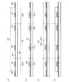
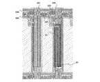
図1(A)は、本発明の発光装置について説明するための上面図、図2、3は、本発明の発光装置の作製方法について説明するための断面図である。図2(A)は、図1(A)における破線A−A’における断面図である。 FIG. 1A is a top view for explaining the light-emitting device of the present invention, and FIGS. 2 and 3 are cross-sectional views for explaining a method for manufacturing the light-emitting device of the present invention. FIG. 2A is a cross-sectional view taken along broken line A-A ′ in FIG.
先ず、図1(A)に示すように、基板101上に、行方向及び列方向に延びた格子状の第1の半導体層102を形成する。第1の半導体層102が形成すると共に、第1の半導体層102に囲まれた領域130内には、図2(A)に示すように島状に分離した第2の半導体層103が複数形成する。ここで、第2の半導体層103は、トランジスタを作製するために形成される層である。そして、後述の工程を経ることにより、第1の半導体層102に囲まれた領域130を一単位とした発光装置が基板201上に複数形成される。なお、本形態では、領域130内に画素部131、駆動回路部132a、132b等を作製するため、図2、3の断面図では、各々の部分について模式的に表している。
First, as shown in FIG. 1A, a lattice-shaped
ここで、基板101について特に限定はないが、ガラスや石英等から成る基板を用いることができる。また、基板101上には、基板101を覆う絶縁層104が形成されていてもよい。絶縁層104は単層または複数の層のいずれから成るものであってもよい。なお、絶縁層104に窒化珪素(数%の酸素を含んでいてもよい)から成る層を含むことにより、基板101から後の工程で作製するトランジスタへの不純物の拡散を阻止することができる。
Here, the
また、第1の半導体層102及び第2の半導体層103は、基板101を覆う半導体層を形成した後、当該半導体層をエッチングによって加工して形成すればよい。ここで、半導体層について特に限定はなく、珪素等を用いて形成することができる。また半導体層の結晶性についても特に限定はなく、結晶質成分を含む半導体層を用いることができる。
The
次に、第1の半導体層102及び第2の半導体層103を覆う絶縁層105を形成する。なお絶縁層105は単層又は複数の層のいずれから成るものであってもよく、例えば酸化珪素、または窒化珪素を用いて形成することができる。
Next, an insulating
なお、絶縁層105の形成前または形成後に、トランジスタの閾値を調節するために、第2の半導体層103にn型又はp型の不純物の添加をしてもよい。n型不純物としては、例えば燐等を用いることができ、p型不純物としては、例えばボロン等を用いることができる。また、第2の半導体層103に不純物を添加するとき、第1の半導体層102にも不純物を添加してもよい。
Note that an n-type or p-type impurity may be added to the
次に、絶縁層105上であって、第2の半導体層103と絶縁層105とが重畳する部分の上方に、ゲート電極として機能する導電層106を形成する。導電層106は、先ず絶縁層105を覆うように導電層を形成した後、当該導電層をエッチングによって加工し、形成すればよい。このとき、基板101は、第1の半導体層102が形成されていることによって基板全体がほぼ等電位に保たれている。従って、ドライエッチング等のプラズマ励起を利用したエッチング方法を用いたときでも、基板内での電位の偏りが生じにくく、静電気に起因した素子の破壊が生じにくい。ここで、導電層106は単層又は複数の層のいずれから成るものであってもよく、例えば、絶縁層105と密着性のよい導電層を絶縁層105と接するように設け、その導電層上に抵抗の低い導電層が積層されたようなものであってもよい。導電層106の形状についても特に限定はなく、例えば側壁に傾斜を有する形状であってもよい。
Next, a
次に、導電層106をマスクとして、第2の半導体層103に不純物を添加する。ここで、n型のトランジスタを作製するときは燐等のn型を付与する不純物を添加すればよく、p型のトランジスタを作製するときは、ボロン等のp型を付与する不純物を添加すればよい。また、n型の不純物を添加するとき、p型のトランジスタの構成要素となる半導体層については、レジスト等のマスクを用いて不純物が添加されないように保護すればよい。p型の不純物を添加するときも、n型のトランジスタの構成要素となる半導体層については、レジスト等のマスクを用いて不純物が添加されないように保護すればよい。また、例えば、レジスト等のマスクを用いずに基板101上の半導体層全てにn型不純物を添加した後、n型を打ち消してp型を付与できるように添加量を調節して、p型のトランジスタの構成要素である半導体層に対してp型の不純物を添加してもよい。
Next, an impurity is added to the
ここで、不純物の添加法について特に限定はなく、例えばドーピング法等を用いることができる。また、第2の半導体層103に不純物を添加すると共に、第1の半導体層102にも不純物を添加しても構わない。第1の半導体層102にも不純物を添加することによって、基板101の全面を等電位となるように保つ効果がより高まる。
Here, the method for adding impurities is not particularly limited, and for example, a doping method or the like can be used. Further, impurities may be added to the
以上のような工程によって、半導体層と絶縁層と導電層とが積層して成るトランジスタ121a、121b、121c、121dを作製することができる。ここで、トランジスタ121a、121bは、画素部131に含まれ、発光素子と接続している。また、トランジスタ121cは駆動回路部132aに含まれ、トランジスタ121dは駆動回路部132bに含まれる。また、画素部131、駆動回路部132a、132bにはそれぞれ、トランジスタ121a、121b、121c、121d以外のトランジスタが含まれていてもよい。なお、トランジスタ121a、121b、121c、121dの構造について特に限定はなく、シングルドレイン構造またはLDD構造、またはLDDとゲート電極として機能する導電層とがオーバーラップしたLDD構造等、いずれの構造のものであってもよい。また、第1の半導体層102が設けられた状態で作製するのであれば、トランジスタ121a、121b、121c、121dを作製する工程について特に限定はなく、所望の構造のトランジスタ121a、121b、121c、121dが形成できるように、適宜工程を決めればよい。また、発光装置に設けられる全てのトランジスタを同じ構造で作製する必要はなく、トランジスタの用途によって適宜作り分ければよい。
Through the above steps,
次に、導電層106等を覆う絶縁層107を形成する。絶縁層107は単層又は複数の層のいずれから成るものであってもよい。本形態では、絶縁層107は絶縁層107aと絶縁層107bの二層から成る。まず、絶縁層107aを形成した後、熱処理をし、さらに絶縁層107aを覆う絶縁層107bを形成する。絶縁層107aについて特に限定はないが、350℃以上の耐熱性を有するような物質、例えば酸化珪素、窒化珪素、数%の酸素を含む窒化珪素、または数%の窒素を含む酸化珪素等の無機物から成ることが好ましい。また、絶縁層107bについて特に限定はないが、表面が平坦な層、例えばアクリル、シロキサンまたはポリイミド等の自己平坦性を有する物質からなる層、または酸化珪素等から成る層を形成後CMP(Chemical and Mechanical Polishing)法等によって平坦化して形成した層であることが好ましい。なお、熱処理の処理条件について特に限定はないが、350〜600℃の温度下で、窒素または水素等のガスが充填された雰囲気で行うことが好ましい。また、熱処理の工程部位についても特に限定はなく、本形態のように一層目の絶縁層107aの形成後でもよいし、または二層目の絶縁層107bの形成後、または絶縁層107aの形成後及び絶縁層107bの形成後でもよい。
Next, an insulating
次に、絶縁層107を貫通して第2の半導体層に至るコンタクトホールを形成する。コンタクトホールは、絶縁層107をエッチングして形成すればよい。このとき、エッチングとしては、ドライエッチングまたはウェットエッチングのいずれの方法を用いてもよいし、両方を組み合わせて用いてもよい。例えば、絶縁層107bをドライエッチングして開孔した後、絶縁層107aをウェットエッチングして開孔し、コンタクトホールを形成してもよい。また、絶縁層107a、107bのいずれもドライエッチングによって開孔してもよい。
Next, a contact hole that penetrates the insulating
なお、コンタクトホールの形成時、基板101は、第1の半導体層102が形成されていることによって基板全体がほぼ等電位に保たれている。従って、ドライエッチング等のプラズマ励起を利用したエッチング方法を用いてコンタクトホールを開孔するときでも、基板内での電位の偏りが生じにくく、静電気に起因した素子の破壊が生じにくい。
Note that when the contact hole is formed, the
次に、配線108、109等を形成する。配線108、109は、導電層を形成した後、当該導電層をエッチングによって加工し、形成すればよい。なお、導電層について特に限定はなく、単層または複数の層のいずれから成るものでもよい。但し、アルミニウムのような低抵抗な物質から成る層を含むように形成することが好ましい。なお、配線108,109を窒化チタン等から成る層によってアルミニウムから成る層を挟むような積層構造にすると、第2の半導体層103と接する部分において第2の半導体層103とアルミニウムから成る層とが接触することを防止でき、また後の工程において発光素子の電極を形成するために酸性の溶液を用いるときにアルミニウムから成る層が腐食されるのを防止できる。本形態のように、配線108と第1の半導体層102とは重畳し、さらに配線108と第1の半導体層102とが接しているとき、配線108をエッチングする工程において、第1の半導体層102もエッチングすればよい。なお、配線108は発光素子に電流を供給するための配線である。本形態のように、第1の半導体層102の上方は、配線109を引き回すための領域として有効に活用することができる。なお、配線108と第1の半導体層102とは必ずしも本形態のように接している必要はなく、間に絶縁層を挟んでいてもよい。また、配線108は、第1の半導体層102に囲まれた領域130内において、各トランジスタに信号を伝達するための配線である。配線108は、先に形成したコンタクトホールを通って、第2の半導体層103に接続している。
Next,
また、絶縁層107が透湿性の高い物質で形成されているときは、配線108,109を形成すると共に、絶縁層107の側壁を覆う導電層を設けることが好ましい。これによって、絶縁層107を通って発光装置外部から発光素子への水分混入を阻止することができる。
In addition, when the insulating
次に、発光素子の電極110を形成する。このとき、発光素子の電極110の一部が、配線109の少なくとも一部と重畳するように形成することによって、発光素子の電極110と配線109とを電気的に接続することができる。発光素子の電極110について特に限定はなく、例えば、可視光を透過できる導電物によって導電層を形成した後、当該導電層をエッチングして加工し、形成することができる。また、可視光を透過できる導電物について特に限定はないが、インジウム錫酸化物(ITO)、酸化珪素を含有するITO、酸化インジウムに2〜20%の酸化亜鉛(ZnO)を混合して成るIZO(Indium Zinc Oxide)等を用いることができる。なお、エッチングはウェットエッチングまたはドライエッチングのいずれの方法を用いて行ってもよく、例えばITO等のエッチングには弱酸性の溶液を用いことができる。また、可視光を透過できる導電物の他、アルミニウム等を用いて形成することもできる。なお、アルミニウムにはリチウム(Li)等のアルカリ金属またはマグネシウム等のアルカリ土類金属が含まれていてもよい。
Next, the
次に、開口部を有する隔壁層111を形成する。隔壁層111は、曲率半径が連続的に変化する形状となるように形成することが好ましい。また、開口部からは発光素子の電極110が露出するようにする。なお、隔壁層111を構成する物質について特に限定はなく、例えば、アクリル、ポリイミド、シロキサン(シリコン(Si)と酸素(O)との結合で骨格構造が構成され、置換基に少なくとも水素を含む有機物)、レジスト等を用いることができる。ここで、アクリル、ポリイミド、レジストは、感光性を有するものであってもよい。なお、隔壁層111は絶縁層107の側壁を必ずしも覆わなくてもよい。
Next, a
次に、発光素子の電極110を覆うように発光層112を形成する。発光層112について特に限定はなく、発光物質を含んで成る層であればよい。例えば、発光性が高くキャリア輸送性が高い物質から成る単層のものでもよいし、または発光性が高い物質とキャリア輸送性が高い物質とを含む単層または複数の層から成るものであってもよい。発光層112を構成する物質についても特に限定はなく、有機物または無機物のいずれか一方若しくは両方を用いることができる。
Next, the
次に、発光素子の電極113を形成する。発光素子の電極113について特に限定はなく、アルミニウムまたは先に記載したような可視光を透過できる導電物を用いて形成することができる。なお、アルミニウムにはリチウム(Li)やマグネシウム等のアルカリ金属またはアルカリ土類金属が含まれていてもよい。
Next, an
なお、発光素子の電極110、113の少なくとも一方は可視光を透過できるように膜厚、材料、積層構造等を調節することが好ましい。
Note that it is preferable to adjust the film thickness, material, stacked structure, and the like so that at least one of the
以上のような工程によって、発光素子の電極110と発光素子の電極113との間に発光層112を挟んで成る発光素子114が作製される。
Through the above-described process, the light-emitting
発光素子114を作製した後、発光素子に水分等が混入するのを阻止するための保護層115を設けてもよい。保護層115は、単層又は複数の層のいずれから成るものであってもよく、窒化珪素等によって形成することができる。
After the light-emitting
以上の工程を経ることによって、図1(B)に表されるように、画素部131、駆動回路部132a、132b、133、画素部および駆動回路部の周辺に設けられた配線109、接続端子134等を含んで成る発光装置が、基板101上に複数作製される。画素部131には、トランジスタと発光素子とを含んで成る画素が行方向及び列方向に複数配列している。なお、図1(B)では、発光装置に含まれる構成要素(画素部131、駆動回路部132a、132b、133、画素部および駆動回路部の周辺に設けられた配線108、接続端子134等)と、第1の半導体層102との位置関係を示すために、第1の半導体層102についても図示している。また、図1(B)には、二つのトランジスタと発光素子とを含んで成る一つの画素について示されているが、画素の構成は、これに限定されるものではない。
Through the above steps, as shown in FIG. 1B, the
なお、以上のような発光装置の製造方法において、配線108、109形成後に生じ得る静電気に起因した素子の損傷を低減するために、ショートリングを利用してもよい。
Note that in the method for manufacturing a light-emitting device as described above, a short ring may be used in order to reduce element damage due to static electricity that may occur after the
次に、基板101を発光装置ごとに切り分ける(つまり分断する。)。このとき、切り込みが入る部分の基板上には、層が積層されていないことが好ましく、特に導電層、有機物から成る層等が積層されていないことが好ましい。
Next, the
次に、発光層が内側に閉じこめられるように、分断後の基板101と基板140とをシール材141を用いて貼り合わせて封止する。このとき、絶縁層107を覆う配線108をさらにシール材141が覆うようにすることが好ましい。また、シール材141は、例えばビスフェノールA型液状樹脂、ビスフェノールA型固形樹脂、含ブロムエポキシ樹脂、ビスフェノールF型樹脂、ビスフェノールAD型樹脂、フェノール型樹脂、クレゾール型樹脂、ノボラック型樹脂、環状脂肪族エポキシ樹脂、エピビス型エポキシ樹脂、グリシジルエステル樹脂、グリジシルアミン系樹脂、複素環式エポキシ樹脂、変性エポキシ樹脂等のエポキシ樹脂等の透湿性の低い物質を含むものであることが好ましい。これによって、絶縁層107または隔壁層111が透湿性の高い物質で形成されているときに、絶縁層107を介して発光素子に水分が拡散することを防止できる。なお、封止後の発光装置内部、つまり基板101と基板140とシール材141とに囲まれた内部は、窒素等の不活性気体、または透湿性の低い樹脂材料等で充填されていてもよいし、または真空になっていてもよい。また、封止後の発光装置内部に吸湿性を有する物質を固定して当該内部に混入した水分などを吸収できるようにし、発光素子が水分等によって劣化するのを防止してもよい。吸湿性を有する物質について特に限定はないが、例えば酸化カルシウムを用いることができる。また当該物質の固定法についても特に限定はなく、例えば基板140の一部に凹部を設け、粒状の酸化カルシウムと固定剤とを含む組成物を当該凹部に注入した後、当該組成物を固化することによって固定することができる。なお固定剤についても特に限定はなく、例えばエステルアクリレート等を用いることができる。また、基板140について特に限定はなく、ガラスや石英、またはプラスチック等から成る基板を用いることができる。
Next, the divided
以上のようにして作製した発光装置は、トランジスタ121a、121b、121c、121dの作製時から配線108、109を形成するに至るまでの間、基板101上に行方向及び列方向に延びた格子状の第1の半導体層102を有し、基板101が等電位となるように保たれ状態で作製されている。従って、当該発光装置では、プラズマ励起を利用した処理等で生じやすい静電気に起因した素子の損傷が低減される。なお、本発明は、大型の基板、特に600mm×720mm以上である大型の基板を用いて一基板から複数の発光装置を形成するときに非常に有効である。
The light-emitting device manufactured as described above has a lattice shape extending in the row direction and the column direction over the
(実施の形態2)
本実施の形態では、実施の形態1で説明した製造方法と本発明の態様について、図4、5を用いて説明する。
(Embodiment 2)
In this embodiment mode, the manufacturing method described in Embodiment Mode 1 and aspects of the present invention will be described with reference to FIGS.
先ず、基板201上に、実施の形態1で示した第1の半導体層102と同様にして、行方向及び列方向に延びた格子状の第1の半導体層202を形成する。第1の半導体層202を形成すると共に、第1の半導体層202に囲まれた領域230内には、実施の形態1で示した第2の半導体層103と同様にして、島状に分離した第2の半導体層203が複数形成される。ここで、第2の半導体層203は、トランジスタを作製するために形成される層である。そして、後述の工程を経ることにより、第1の半導体層202に囲まれた領域230を一単位とした発光装置が基板201上に複数形成される。なお、本形態では、領域230内に画素部231、駆動回路部232a、232b等を作製するため、図4、5の断面図では、各々の部分について模式的に表している。
First, in the same manner as the
ここで、基板201について特に限定はなく、実施の形態1で示した基板101と同様のものを用いることができる。また、基板201上には、基板201を覆う絶縁層204が形成されていてもよい。絶縁層204についても、特に限定はなく、実施の形態1で示した絶縁層104と同様のものを用いればよい。
Here, there is no particular limitation on the substrate 201, and a substrate similar to the
また、第1の半導体層202及び第2の半導体層203は、基板201を覆う半導体層を形成した後、当該半導体層をエッチングによって加工し、形成すればよい。半導体層について特に限定はなく、珪素等を用いて形成することができる。また半導体層の結晶性についても特に限定はなく、結晶質成分を含む半導体層を用いることができる。
The
次に、第1の半導体層202及び第2の半導体層203を覆う絶縁層205を形成する。絶縁層205について特に限定はなく、実施の形態1で示した絶縁層105と同様にして形成すればよい。
Next, an insulating
なお、絶縁層205の形成前または形成後に、トランジスタの閾値を調節するために、第2の半導体層203にn型又はp型の不純物の添加をしてもよい。n型不純物としては、例えば燐等を用いることができ、p型不純物としては、例えばボロン等を用いることができる。また、第2の半導体層203に不純物を添加するとき、第1の半導体層202にも不純物を添加してもよい。
Note that an n-type or p-type impurity may be added to the
次に、絶縁層205上であって、第2の半導体層203と絶縁層205とが重畳する部分の上方に、ゲート電極として機能する導電層206を形成する。導電層206は、先ず絶縁層205を覆うように導電層を形成した後、当該導電層をエッチングによって加工し、形成すればよい。このとき、基板201は、第1の半導体層202が形成されていることによって基板面全体がほぼ等電位に保たれている。従って、ドライエッチング等のプラズマ励起を利用したエッチング方法を用いたときでも、基板内での電位の偏りが生じにくく、静電気に起因した素子の破壊が生じにくい。ここで、導電層206は単層又は複数の層のいずれから成るものであってもよく、例えば、絶縁層205と密着性のよい導電層を絶縁層205と接するように設け、その導電層上に抵抗の低い導電層が積層されたようなものであってもよい。導電層206の形状についても特に限定はなく、例えば側壁に傾斜を有する形状であってもよい。
Next, a
次に、導電層206をマスクとして、第2の半導体層203に不純物を添加する。ここで、n型のトランジスタを作製するときは燐等のn型を付与する不純物を添加すればよく、p型のトランジスタを作製するときは、ボロン等のp型を付与する不純物を添加すればよい。また、n型の不純物を添加するとき、p型のトランジスタの構成要素となる半導体層については、レジスト等のマスクを用いて不純物が添加されないように保護すればよい。p型の不純物を添加するときも、n型のトランジスタの構成要素となる半導体層については、レジスト等のマスクを用いて不純物が添加されないように保護すればよい。また、例えば、レジスト等のマスクを用いずに基板201上の半導体層全てにn型不純物を添加した後、n型を打ち消してp型を付与できるように添加量を調節して、p型のトランジスタの構成要素である半導体層に対してp型の不純物を添加してもよい。
Next, an impurity is added to the
ここで、不純物の添加法について特に限定はなく、例えばドーピング法等を用いることができる。また、第2の半導体層203に不純物を添加すると共に、第1の半導体層202にも不純物を添加しても構わない。第1の半導体層202にも不純物を添加することによって、基板201を等電位となるように保つ効果がより高まる。
Here, the method for adding impurities is not particularly limited, and for example, a doping method or the like can be used. Further, an impurity may be added to the
以上のような工程によって、半導体層と絶縁層と導電層とが積層して成るトランジスタ221a、221b、221c、221dを作製することができる。ここで、トランジスタ221a、221bは、画素部231に含まれ、発光素子と接続している。また、トランジスタ221cは駆動回路部232aに含まれ、トランジスタ221dは駆動回路部232bに含まれる。また、画素部231、駆動回路部232a、232bにはそれぞれ、トランジスタ221a、221b、221c、221d以外のトランジスタが含まれていてもよい。なお、トランジスタ221a、221b、221c、221dの構造について特に限定はなく、シングルドレイン構造またはLDD構造、またはLDDとゲート電極として機能する導電層とがオーバーラップしたLDD構造等、いずれの構造のものであってもよい。また、第1の半導体層202が設けられた状態で作製するのであれば、トランジスタ221a、221b、221c、221dを作製する工程について特に限定はなく、所望の構造のトランジスタ221a、221b、221c、221dが形成できるように、適宜工程を決めればよい。また、発光装置に設けられる全てのトランジスタを同じ構造で作製する必要はなく、トランジスタの用途によって適宜作り分ければよい。
Through the above steps, the
次に、導電層206等を覆う絶縁層207を形成する。絶縁層207は単層又は複数の層のいずれから成るものであってもよい。本形態では、絶縁層207は絶縁層207aと絶縁層207bの二層から成るものを形成する。まず、絶縁層207aを形成した後、さらに絶縁層207aを覆う絶縁層207bを形成した後、熱処理する。絶縁層207a、207bについて特に限定はないが、350℃以上の耐熱性を有するような物質、例えば酸化珪素、窒化珪素、数%の酸素を含む窒化珪素、または数%の窒素を含む酸化珪素等の無機物から成ることが好ましい。なお、熱処理の処理条件について特に限定はないが、350〜600℃の温度下で、窒素または水素等のガスが充填された雰囲気で行うことが好ましい。また、熱処理の工程部位についても特に限定はなく、本形態のように一層目の絶縁層207aの形成後でもよいし、または二層目の絶縁層207bの形成後、または絶縁層207aの形成後及び絶縁層207bの形成後でもよい。
Next, an insulating
次に、絶縁層207を貫通して第2の半導体層203に至るコンタクトホールを形成する。コンタクトホールは、絶縁層207をエッチングして形成すればよい。このとき、エッチングとしては、ドライエッチングまたはウェットエッチングのいずれの方法を用いてもよいし、両方を組み合わせて用いてもよい。例えば、絶縁層207bをウエットエッチングして開孔した後、絶縁層207aをドライエッチングして開孔し、コンタクトホールを形成してもよい。また、絶縁層207a、207bのいずれもドライエッチングによって開孔してもよい。
Next, a contact hole that penetrates the insulating
なお、コンタクトホールの形成時、基板201は、第1の半導体層202が形成されていることによって基板面全体がほぼ等電位に保たれている。従って、ドライエッチング等のプラズマ励起を利用したエッチング方法を用いてコンタクトホールを開孔するときでも、基板面内での電位の偏りが生じにくく、静電気に起因した素子の破壊が生じにくい。
Note that when the contact hole is formed, the entire surface of the substrate 201 is kept substantially equipotential because the
次に、配線208、209等を形成する。配線208、209は、導電層を形成した後、当該導電層をエッチングによって加工し、形成すればよい。なお、導電層形成後に、熱処理を行い、シンタリングしてもよい。導電層について特に限定はなく、単層または複数の層のいずれから成るものでもよい。但し、アルミニウムのような低抵抗な物質から成る層を含むように形成することが好ましい。なお、配線208,209を窒化チタン等から成る層によってアルミニウムから成る層を挟むような積層構造にすると、第2の半導体層203と接する部分において第2の半導体層203とアルミニウムから成る層とが接触することを防止でき、また後の工程において発光素子の電極を形成するために酸性の溶液を用いるときにアルミニウムから成る層が腐食されるのを防止できる。なお、配線208は発光素子に電流を供給するための配線である。配線208と第1の半導体層202とは重畳している。このように、第1の半導体層202の上方は配線208を引き回すための領域として有効に活用することができる。なお、配線209は、第1の半導体層202に囲まれた領域230内において、各トランジスタに信号を伝達するための配線である。配線209は、先に形成したコンタクトホールを通って、第2の半導体層203に接続している。
Next,
次に、配線209を覆う絶縁層210を形成する。絶縁層210について特に限定はないが、表面が平坦な層、例えばアクリル、シロキサンまたはポリイミド等の自己平坦性を有する物質からなる層、または酸化珪素等から成る層を形成後CMP(Chemical and Mechanical Polishing)法等によって平坦化して形成した層であることが好ましい。また、絶縁層210がシロキサンから成る場合は、絶縁層210を焼成するための熱処理を行ってもよい。
Next, an insulating
次に、絶縁層210を貫通して配線209に至るコンタクトホールを形成する。また、コンタクトホールを形成すると共に、配線208の一部が露出するように開口部を形成する。コンタクトホール等は、絶縁層210をエッチングして形成すればよい。このとき、エッチングとしては、ドライエッチングまたはウェットエッチングのいずれの方法を用いてもよいし、両方を組み合わせて用いてもよい。
Next, a contact hole that penetrates the insulating
なお、コンタクトホールの形成時、基板201は、第1の半導体層202が形成されていることによって基板全体がほぼ等電位に保たれる。従って、ドライエッチング等のプラズマ励起を利用したエッチング方法を用いてコンタクトホールを開孔するときでも、基板内での電位の偏りが生じにくく、静電気に起因した素子の破壊が生じにくい。
Note that when the contact hole is formed, the substrate 201 is maintained at substantially the same potential because the
次に、絶縁層210を貫通するコンタクトホールを通って配線209に至る発光素子の電極211を形成する。発光素子の電極211について特に限定はなく、例えば、可視光を透過できる導電物によって導電層を形成した後、当該導電層をエッチングして加工し、形成することができる。また、可視光を透過できる導電物について特に限定はないが、インジウム錫酸化物(ITO)、酸化珪素を含有するITO、酸化インジウムに2〜20%の酸化亜鉛(ZnO)を混合して成るIZO(Indium Zinc Oxide)等を用いることができる。なお、エッチングはウェットエッチングまたはドライエッチングのいずれの方法を用いて行ってもよく、例えばITO等のエッチングには弱酸性の溶液を用いことができる。また、可視光を透過できる導電物の他、アルミニウム等を用いて形成することもできる。なお、アルミニウムにはリチウム(Li)等のアルカリ金属またはマグネシウム等のアルカリ土類金属が含まれていてもよい。
Next, an
次に、開口部を有する隔壁層212を形成する。隔壁層212は、曲率半径が連続的に変化する形状となるように形成することが好ましい。また、開口部からは発光素子の電極211が露出するようにする。なお、隔壁層212を構成する物質について特に限定はなく、例えば、アクリル、ポリイミド、シロキサン(シリコン(Si)と酸素(O)との結合で骨格構造が構成され、置換基に少なくとも水素を含む物質)、レジスト等を用いることができる。ここで、アクリル、ポリイミド、レジストは、感光性を有するものであってもよい。なお、図3(B)と同様に隔壁層212は、絶縁層210の側壁を覆っていてもよい。
Next, the
次に、発光素子の電極211を覆うように発光層213を形成する。発光層213について特に限定はなく、実施の形態1で示した発光層112と同様のものでよい。
Next, the
次に、発光素子の電極214を形成する。発光素子の電極214について特に限定はなく、アルミニウムまたは先に記載したような可視光を透過できる導電物を用いて形成することができる。なお、アルミニウムにはリチウム(Li)やマグネシウム等のアルカリ金属またはアルカリ土類金属が含まれていてもよい。
Next, an
なお、発光素子の電極211、214の少なくとも一方は可視光を透過できるように膜厚、材料、積層構造等を調節することが好ましい。
Note that it is preferable to adjust the film thickness, material, stacked structure, and the like so that at least one of the
以上のような工程によって、発光素子の電極211と発光素子の電極214との間に発光層213を挟んで成る発光素子215が作製される。
Through the above-described process, the light-emitting
発光素子215を作製した後、発光素子に水分等が混入するのを阻止するための保護層216を設けてもよい。保護層216は、単層又は複数の層のいずれから成るものであってもよく、窒化珪素等によって形成することができる。
After the light-emitting
以上の工程を経ることによって、画素部231、駆動回路部232a、232b、画素部および駆動回路部の周辺に設けられた配線208、接続端子等を含んで成る発光装置が、基板201上に複数作製される。画素部231には、トランジスタと発光素子とを含んで成る画素が行方向及び列方向に複数配列している。なお、発光装置に含まれる構成要素(画素部231、駆動回路部232a、232b、画素部および駆動回路部の周辺に設けられた配線208、接続端子等)と、第1の半導体層202との位置関係は、実施の形態1において図1(B)に示したものと同様である。但し、発光装置の構成は、図1(B)に示したものには限定されない。
Through the above steps, a plurality of light-emitting devices including the
次に、基板201を発光装置ごとに切り分ける(つまり分断する。)。このとき、基板上の分断部には、層が積層されていないことが好ましく、特に導電層、有機物から成る層等が積層されていないことが好ましい。 Next, the substrate 201 is cut (that is, divided) for each light emitting device. At this time, it is preferable that no layer is stacked on the dividing portion on the substrate, and it is particularly preferable that a conductive layer, a layer made of an organic material, or the like is not stacked.
次に、発光層が内側に閉じこめられるように、分断後の基板201と基板240とをシール材241を用いて貼り合わせて封止する。このとき、絶縁層210に形成された開口部がシール材241によって埋め込まれるようにすることが好ましい。また、シール材241は、例えばビスフェノールA型液状樹脂、ビスフェノールA型固形樹脂、含ブロムエポキシ樹脂、ビスフェノールF型樹脂、ビスフェノールAD型樹脂、フェノール型樹脂、クレゾール型樹脂、ノボラック型樹脂、環状脂肪族エポキシ樹脂、エピビス型エポキシ樹脂、グリシジルエステル樹脂、グリジシルアミン系樹脂、複素環式エポキシ樹脂、変性エポキシ樹脂等のエポキシ樹脂等の透湿性の低い物質を含むものであることが好ましい。これによって、絶縁層210または隔壁層212が透湿性の高い物質で形成されているときに、絶縁層210を介して発光素子215へ水分が拡散することを防止できる。なお、封止後の発光装置内部、つまり基板201と基板240とシール材241とに囲まれた内部は、窒素等の不活性気体、または透湿性の低い樹脂材料等で充填されていてもよいし、または真空になっていてもよい。また、封止後の発光装置内部に吸湿性を有する物質を固定して当該内部に混入した水分などを吸収できるようにし、発光素子が水分等によって劣化するのを防止してもよい。吸湿性を有する物質について特に限定はないが、例えば酸化カルシウムを用いることができる。また当該物質の固定法についても特に限定はなく、例えば基板240の一部に凹部を設け、粒状の酸化カルシウムと固定剤とを含む組成物を当該凹部に注入した後、当該組成物を固化することによって固定することができる。なお固定剤についても特に限定はなく、例えばエステルアクリレート等を用いることができる。また、基板240について特に限定はなく、ガラスや石英、またはプラスチック等から成る基板を用いることができる。
Next, the separated substrate 201 and the
以上のようにして作製した発光装置は、発光装置を製造する間、基板201上に行方向及び列方向に延びた格子状の第1の半導体層202を有し、基板201が等電位となるように保たれ状態で作製されている。従って、当該発光装置では、プラズマ励起を利用した処理等で生じやすい静電気に起因した素子の損傷が低減される。なお、本発明は、大型の基板、特に600mm×720mm以上である大型の基板を用いて一基板から複数の発光装置を形成するときに非常に有効である。
The light-emitting device manufactured as described above includes the
(実施の形態3)
本実施の形態では、実施の形態1、2に示したような本発明を適用して製造した発光装置について説明する。
(Embodiment 3)
In this embodiment mode, a light-emitting device manufactured by applying the present invention as shown in Embodiment Modes 1 and 2 will be described.
本形態では、本発明を適用した発光装置の態様について説明する。但し、本発明の発光装置の構造および発光装置を構成する物質等は、本形態に示すものに限定されない。 In this embodiment mode, a mode of a light-emitting device to which the present invention is applied will be described. However, the structure of the light-emitting device of the present invention and the substances constituting the light-emitting device are not limited to those shown in this embodiment mode.
図3(c)または図5(C)で表されるような発光装置において、発光素子114の構成要素である発光層112、および発光素子215の構成要素である発光層213は、複数の層から成る。複数の層は、キャリア輸送性の高い物質とキャリア注入性の高い物質とから選ばれた物質から成る層を組み合わせて構成されたものであり、一部に発光性の高い物質を含むものである。発光層112を構成する物質は無機物でも有機物でも構わない。また、有機物の場合、低分子でも高分子でも構わない。
In the light-emitting device as illustrated in FIG. 3C or FIG. 5C, the light-emitting
ここで、発光物質としては、4−ジシアノメチレン−2−メチル−6−[2−(1,1,7,7−テトラメチルジュロリジン−9−イル)エテニル] −4H−ピラン(略称:DCJT)、4−ジシアノメチレン−2−tert−ブチル−6−[2−(1,1,7,7−テトラメチルジュロリジン−9−イル)エテニル ]−4H−ピラン(略称:DCJTB)、ペリフランテン、2,5−ジシアノ−1,4−ビス[2−(10−メトキシ−1,1,7,7−テトラメチルジュロリジン−9−イル)エテニル]ベンゼン、N,N’−ジメチルキナクリドン(略称:DMQd)、クマリン6、クマリン545T、トリス(8−キノリノラト)アルミニウム(略称:Alq3)、9,9’−ビアントリル、9,10−ジフェニルアントラセン(略称:DPA)や9,10−ビス(2−ナフチル)アントラセン(略称:DNA)等を用いることができる。また、この他の物質でもよい。 Here, as the light-emitting substance, 4-dicyanomethylene-2-methyl-6- [2- (1,1,7,7-tetramethyljulolidin-9-yl) ethenyl] -4H-pyran (abbreviation: DCJT) ), 4-dicyanomethylene-2-tert-butyl-6- [2- (1,1,7,7-tetramethyljulolidin-9-yl) ethenyl] -4H-pyran (abbreviation: DCJTB), periflanthene, 2,5-dicyano-1,4-bis [2- (10-methoxy-1,1,7,7-tetramethyljulolidin-9-yl) ethenyl] benzene, N, N′-dimethylquinacridone (abbreviation: DMQd), coumarin 6, coumarin 545T, tris (8-quinolinolato) aluminum (abbreviation: Alq 3 ), 9,9′-bianthryl, 9,10-diphenylanthracene (abbreviation: DPA) and 9,10-bis (2- Naf Chill) anthracene (abbreviation: DNA) or the like can be used. Other substances may also be used.
なお、以上のような一重項励起発光物質の他、金属錯体などを含む三重項励起物質を用いても良い。例えば、赤色の発光性の画素、緑色の発光性の画素及び青色の発光性の画素のうち、輝度半減時間が比較的短い赤色の発光性の画素を三重項励起発光物質で形成し、他を一重項励起発光物質で形成する。三重項励起発光物質は発光効率が良いので、同じ輝度を得るのに消費電力が少なくて済むという特徴がある。すなわち、赤色画素に適用した場合、発光素子に流す電流量が少なくて済むので、信頼性を向上させることができる。低消費電力化として、赤色の発光性の画素と緑色の発光性の画素とを三重項励起発光物質で形成し、青色の発光性の画素を一重項励起発光物質で形成しても良い。人間の視感度が高い緑色の発光素子も三重項励起発光物質で形成することで、より低消費電力化を図ることができる。 In addition to the singlet excited luminescent material as described above, a triplet excited material containing a metal complex or the like may be used. For example, among red light emitting pixels, green light emitting pixels, and blue light emitting pixels, a red light emitting pixel having a relatively short luminance half time is formed of a triplet excitation light emitting material, and the other It is formed of a singlet excited luminescent material. A triplet excited luminescent substance has a feature that it has a high luminous efficiency, so that less power is required to obtain the same luminance. That is, when applied to a red pixel, the amount of current flowing through the light emitting element can be reduced, so that reliability can be improved. As a reduction in power consumption, a red light-emitting pixel and a green light-emitting pixel may be formed using a triplet excitation light-emitting material, and a blue light-emitting pixel may be formed using a singlet excitation light-emitting material. By forming a green light-emitting element having high human visibility with a triplet-excited light-emitting substance, power consumption can be further reduced.
三重項励起発光物質の一例としては、金属錯体をドーパントとして用いたものがあり、第三遷移系列元素である白金を中心金属とする金属錯体、イリジウムを中心金属とする金属錯体などが知られている。三重項励起発光物質としては、これらの化合物に限られることはなく、上記構造を有し、且つ中心金属に周期表の8〜10属に属する元素を有する化合物を用いることも可能である。 Examples of triplet excited luminescent materials include those using metal complexes as dopants, and metal complexes having a third transition series element platinum as the central metal and metal complexes having iridium as the central metal are known. Yes. The triplet excited light-emitting substance is not limited to these compounds, and it is also possible to use a compound having the above structure and having an element belonging to Group 8 to 10 in the periodic table as a central metal.
キャリア輸送性の高い物質のうち、特に電子輸送性の高い物質としては、例えばトリス(8−キノリノラト)アルミニウム(略称:Alq3)、トリス(5−メチル−8−キノリノラト)アルミニウム(略称:Almq3)、ビス(10−ヒドロキシベンゾ[h]−キノリナト)ベリリウム(略称:BeBq2)、ビス(2−メチル−8−キノリノラト)−4−フェニルフェノラト−アルミニウム(略称:BAlq)など、キノリン骨格またはベンゾキノリン骨格を有する金属錯体等が挙げられる。また正孔輸送性の高い物質としては、例えば4,4'−ビス[N−(1−ナフチル)−N−フェニル−アミノ]−ビフェニル(略称:α−NPD)や4,4'−ビス[N−(3−メチルフェニル)−N−フェニル−アミノ]−ビフェニル(略称:TPD)や4,4',4''−トリス(N,N−ジフェニル−アミノ)−トリフェニルアミン(略称:TDATA)、4,4',4''−トリス[N−(3−メチルフェニル)−N−フェニル−アミノ]−トリフェニルアミン(略称:MTDATA)などの芳香族アミン系(即ち、ベンゼン環−窒素の結合を有する)の化合物が挙げられる。また、キャリア注入性の高い物質のうち、特に電子注入性の高い物質としては、フッ化リチウム(LiF)、フッ化セシウム(CsF)、フッ化カルシウム(CaF2)等のようなアルカリ金属又はアルカリ土類金属の化合物が挙げられる。また、この他、Alq3のような電子輸送性の高い物質とマグネシウム(Mg)のようなアルカリ土類金属との混合物であってもよい。また、正孔注入性の高い物質としては、例えば、モリブデン酸化物(MoOx)やバナジウム酸化物(VOx)、ルテニウム酸化物(RuOx)、タングステン酸化物(WOx)、マンガン酸化物(MnOx)等の金属酸化物が挙げられる。また、この他、フタロシアニン(略称:H2Pc)や銅フタロシアニン(CuPC)等のフタロシアニン系の化合物が挙げられる。また、正孔注入性が高く正孔輸送性も高い物質であるポリスチレンスルフォン酸(PSS)とポリエチレンジオキシチオフェン(PEDOT)とを混合した高分子材料等を用いてもよい。 Among substances having a high carrier transport property, examples of the substance having a particularly high electron transport property include, for example, tris (8-quinolinolato) aluminum (abbreviation: Alq 3 ), tris (5-methyl-8-quinolinolato) aluminum (abbreviation: Almq 3). ), Bis (10-hydroxybenzo [h] -quinolinato) beryllium (abbreviation: BeBq 2 ), bis (2-methyl-8-quinolinolato) -4-phenylphenolato-aluminum (abbreviation: BAlq), or the like, And metal complexes having a benzoquinoline skeleton. As a substance having a high hole-transport property, for example, 4,4′-bis [N- (1-naphthyl) -N-phenyl-amino] -biphenyl (abbreviation: α-NPD), 4,4′-bis [ N- (3-methylphenyl) -N-phenyl-amino] -biphenyl (abbreviation: TPD) or 4,4 ′, 4 ″ -tris (N, N-diphenyl-amino) -triphenylamine (abbreviation: TDATA) ), 4,4 ′, 4 ″ -tris [N- (3-methylphenyl) -N-phenyl-amino] -triphenylamine (abbreviation: MTDATA) (ie, benzene ring-nitrogen) And a compound having a bond of In addition, among substances having a high carrier-injecting property, substances having a particularly high electron-injecting property include alkali metals or alkalis such as lithium fluoride (LiF), cesium fluoride (CsF), and calcium fluoride (CaF 2 ). Examples include earth metal compounds. In addition, a mixture of a substance having a high electron transport property such as Alq 3 and an alkaline earth metal such as magnesium (Mg) may be used. Examples of the material having a high hole injection property include molybdenum oxide (MoOx), vanadium oxide (VOx), ruthenium oxide (RuOx), tungsten oxide (WOx), and manganese oxide (MnOx). A metal oxide is mentioned. In addition, phthalocyanine compounds such as phthalocyanine (abbreviation: H 2 Pc) and copper phthalocyanine (CuPC) can be given. Alternatively, a polymer material obtained by mixing polystyrene sulfonic acid (PSS) and polyethylenedioxythiophene (PEDOT), which are substances having a high hole injecting property and a high hole transporting property, may be used.
なお、高分子系有機発光材料は低分子系に比べて物理的強度が高く、素子の耐久性が高い。また塗布により成膜することが可能であるので、素子の作製が比較的容易である。 The high molecular weight organic light emitting material has higher physical strength than the low molecular weight material, and the durability of the device is high. In addition, since the film can be formed by coating, the device can be manufactured relatively easily.
また、第2の半導体層103または第2の半導体層203として用いることのできる結晶質成分を含む半導体層の具体例としては、単結晶または多結晶性の珪素、或いはシリコンゲルマニウム等から成るものが挙げられる。これらはレーザ結晶化によって形成されたものでもよいし、例えばニッケル等を用いた固相成長法による結晶化によって形成されたものでもよい。また、レーザ結晶化と固相成長法とを組み合わせて形成されたものでもよい。この他、セミアモルファス半導体も、第2の半導体層203として用いることができる。
As a specific example of a semiconductor layer containing a crystalline component that can be used as the
なお、セミアモルファスな半導体とは、次のようなものである。非晶質と結晶構造(単結晶、多結晶を含む)の中間的な構造を有し、自由エネルギー的に安定な第3の状態を有する半導体であって、短距離秩序を持ち格子歪みを有する結晶質な領域を含んでいるものである。また少なくとも膜中の一部の領域には、0.5〜20nmの結晶粒を含んでいる。L−Oフォノンに由来するラマンスペクトルが520cm-1よりも低波数側にシフトしている。X線回折ではSi結晶格子に由来するとされる(111)、(220)の回折ピークが観測される。未結合手(ダングリングボンド)を終端するために水素またはハロゲンを少なくとも1原子%またはそれ以上含ませている。所謂微結晶半導体(マイクロクリスタル半導体)とも言われている。珪化物気体をグロー放電分解(プラズマCVD)して形成する。珪化物気体としては、SiH4、その他にもSi2H6、SiH2Cl2、SiHCl3、SiCl4、SiF4などを用いることができる。この珪化物気体をH2、又は、H2とHe、Ar、Kr、Neから選ばれた一種または複数種の希ガス元素で希釈しても良い。希釈率は2〜1000倍の範囲。圧力は概略0.1Pa〜133Paの範囲、電源周波数は1MHz〜120MHz、好ましくは13MHz〜60MHz。基板加熱温度は300℃以下でよく、好ましくは100〜250℃、膜中の不純物元素として、酸素、窒素、炭素などの大気成分の不純物は1×1020atoms/cm3以下とすることが望ましく、特に、酸素濃度は5×1019atoms/cm3以下、好ましくは1×1019atoms/cm3以下とする。なお、セミアモルファスなものを有する半導体を用いたTFT(薄膜トランジスタ)の移動度はおよそ1〜10m2/Vsecとなる。 The semi-amorphous semiconductor is as follows. A semiconductor having an intermediate structure between amorphous and crystalline (including single crystal and polycrystal) and having a third state that is stable in terms of free energy, has a short-range order, and has a lattice distortion. It contains a crystalline region. Further, at least a partial region in the film contains crystal grains of 0.5 to 20 nm. The Raman spectrum derived from the L—O phonon is shifted to the lower wavenumber side than 520 cm −1 . In X-ray diffraction, diffraction peaks of (111) and (220) that are derived from the Si crystal lattice are observed. In order to terminate dangling bonds (dangling bonds), hydrogen or halogen is contained at least 1 atomic% or more. It is also called a so-called microcrystalline semiconductor (microcrystal semiconductor). A silicide gas is formed by glow discharge decomposition (plasma CVD). As the silicide gas, SiH 4 , Si 2 H 6 , SiH 2 Cl 2 , SiHCl 3 , SiCl 4 , SiF 4 or the like can be used. This silicide gas may be diluted with H 2 , or H 2 and one or more kinds of rare gas elements selected from He, Ar, Kr, and Ne. The dilution rate is in the range of 2 to 1000 times. The pressure is generally in the range of 0.1 Pa to 133 Pa, and the power supply frequency is 1 MHz to 120 MHz, preferably 13 MHz to 60 MHz. The substrate heating temperature may be 300 ° C. or less, preferably 100 to 250 ° C. As an impurity element in the film, impurities of atmospheric components such as oxygen, nitrogen, and carbon are desirably 1 × 10 20 atoms / cm 3 or less. In particular, the oxygen concentration is 5 × 10 19 atoms / cm 3 or less, preferably 1 × 10 19 atoms / cm 3 or less. Note that the mobility of a TFT (thin film transistor) using a semi-amorphous semiconductor is approximately 1 to 10 m 2 / Vsec.
また、発光素子114、215は、発光素子の電極110、211が陽極として機能し、発光素子の電極113、214が陰極として機能する構成であってもよいし、或いは発光素子の電極110、211が陰極として機能し、発光素子の電極113、214が陽極として機能する構成であってもよい。但し、前者の場合、発光素子と接続しているトランジスタはPチャネル型トランジスタであり、後者の場合、トランジスタはNチャネル型トランジスタである。
The
本発明の発光装置の画素部は、以上に述べたような発光素子114、215とそれを駆動するためのトランジスタとが含まれる画素が複数、マトリクス状に配列して成る。なお、発光層は、発光波長帯の異なる発光層を画素毎に形成して、カラー表示を行う構成としても良い。典型的には、R(赤)、G(緑)、B(青)の各色に対応した発光層を形成する。この場合にも、画素の光放射側にその発光波長帯の光を透過するフィルター(着色層)を設けた構成とすることで、色純度の向上や、画素部の鏡面化(映り込み)の防止を図ることができる。フィルター(着色層)を設けることで、従来必要であるとされていた円偏光板などを省略することが可能となり、発光層から放射される光の損失を無くすことができる。さらに、斜方から画素部(表示画面)を見た場合に起こる色調の変化を一層低減することができる。
The pixel portion of the light emitting device of the present invention includes a plurality of pixels including the
また、上記のように各色に対応した発光層を設けて、カラー表示を行う以外に、発光層は単色、例えば白色の発光を呈する構成とすることもできる。白色発光材料を用いる場合には、画素の光放射側に特定の波長の光を透過するフィルター(着色層)を設けた構成としてカラー表示を可能にすることができる。 In addition to providing a light emitting layer corresponding to each color and performing color display as described above, the light emitting layer can be configured to emit a single color, for example, white light. In the case of using a white light emitting material, color display can be made possible by providing a filter (colored layer) that transmits light of a specific wavelength on the light emission side of the pixel.
なお、 白色に発光する発光層を形成するには、例えば、Alq3、部分的にナイルレッドをドープしたAlq3、p−EtTAZ、TPD(芳香族ジアミン)を蒸着法により順次積層することで白色を得ることができる。また、スピンコートを用いた塗布法により発光層を形成する場合には、塗布した後、真空加熱で焼成することが好ましい。例えば、ポリ(エチレンジオキシチオフェン)/ポリ(スチレンスルホン酸)水溶液(PEDOT/PSS)を全面に塗布、焼成し、その後、色素(1,1,4,4−テトラフェニル−1,3−ブタジエン(TPB)、4−ジシアノメチレン−2−メチル−6−(p−ジメチルアミノ−スチリル)−4H−ピラン(DCM1)、ナイルレッド、クマリン6など)ドープしたポリビニルカルバゾール(PVK)溶液を全面に塗布、焼成すればよい。 In order to form a light emitting layer that emits white light, for example, Alq 3, partially Alq doped with Nile Red 3, p-EtTAZ, TPD white by sequentially laminated by an evaporation method (aromatic diamine) Can be obtained. Moreover, when forming a light emitting layer by the apply | coating method using spin coating, after apply | coating, it is preferable to bake by vacuum heating. For example, a poly (ethylenedioxythiophene) / poly (styrenesulfonic acid) aqueous solution (PEDOT / PSS) is applied to the entire surface and fired, and then a dye (1,1,4,4-tetraphenyl-1,3-butadiene (TPB), 4-dicyanomethylene-2-methyl-6- (p-dimethylamino-styryl) -4H-pyran (DCM1), Nile Red, Coumarin 6 etc.) doped polyvinylcarbazole (PVK) solution is applied over the entire surface What is necessary is just to bake.
発光層は上記のように多層から成るもの以外に単層で形成することもできる。この場合、ポリビニルカルバゾール(PVK)に1,3,4−オキサジアゾール誘導体(PBD)を分散させてもよい。また、30wt%のPBDを分散し、4種類の色素(TPB、クマリン6、DCM1、ナイルレッド)を適当量分散することで白色発光が得られる。 The light emitting layer can be formed as a single layer in addition to the multilayer as described above. In this case, a 1,3,4-oxadiazole derivative (PBD) may be dispersed in polyvinyl carbazole (PVK). Further, white light emission can be obtained by dispersing 30 wt% PBD and dispersing an appropriate amount of four kinds of dyes (TPB, coumarin 6, DCM1, Nile red).
本発明の発光装置の構成要素である発光素子は、順方向にバイアスすることで発光する。発光素子を用いて形成する表示装置の画素は、アクティブマトリクス方式で駆動することができる。いずれにしても、個々の画素は、ある特定のタイミングで順方向バイアスを印加して発光させることとなるが、ある一定期間は非発光状態となっている。この非発光時間に逆方向のバイアスを印加することで発光素子の信頼性を向上させることができる。発光素子では、一定駆動条件下で発光強度が低下する劣化や、画素内で非発光領域が拡大して見かけ上輝度が低下する劣化モードがあるが、順方向及び逆方向にバイアスを印加する交流的な駆動を行うことで、劣化の進行を遅くすることができ、発光装置の信頼性を向上させることができる。 The light emitting element which is a component of the light emitting device of the present invention emits light by being forward biased. A pixel of a display device formed using a light-emitting element can be driven by an active matrix method. In any case, each pixel emits light by applying a forward bias at a specific timing, but is in a non-light emitting state for a certain period. By applying a reverse bias during this non-light emitting time, the reliability of the light emitting element can be improved. The light emitting element has a degradation mode in which the light emission intensity decreases under a constant driving condition and a degradation mode in which the non-light emitting area is enlarged in the pixel and the luminance is apparently decreased. However, alternating current that applies a bias in the forward and reverse directions. By performing a typical drive, the progress of deterioration can be slowed and the reliability of the light emitting device can be improved.
なお、以上に述べたような構成は、図3(C)または図5(C)に示したような本発明の発光装置に限らず、その他の本発明の発光装置に適用しても構わない。 Note that the structure described above is not limited to the light emitting device of the present invention as shown in FIG. 3C or FIG. 5C, and may be applied to other light emitting devices of the present invention. .
(実施の形態4)
本実施例では、本発明の発光装置において発光素子を駆動するために画素部に設けられている回路について説明する。但し、発光装置を駆動するための回路は、本実施例で示すものには限定されない。
(Embodiment 4)
In this embodiment, a circuit provided in a pixel portion in order to drive a light emitting element in a light emitting device of the present invention will be described. However, the circuit for driving the light emitting device is not limited to that shown in this embodiment.
図6(A)に示すように、発光素子301には、各々の発光素子を駆動するための回路が接続されている。当該回路は、それぞれ、映像信号によって発光素子301の発光・非発光を決定する駆動用トランジスタ321と、前記映像信号の入力を制御するスイッチング用トランジスタ322と、前記映像信号に関わらず発光素子301を非発光状態にする消去用トランジスタ323とを有する。ここで、スイッチング用トランジスタ322のソース(又はドレイン)はソース信号線331と接続し、駆動用トランジスタ321のソース及び消去用トランジスタ323のソースはソース信号線331と並列するように延びた電流供給線332と接続し、スイッチング用トランジスタ322のゲートは第1の走査線333と接続し消去用トランジスタ323のゲートは、第1の走査線333と並列に延びた第2の走査線334と接続している。また、駆動用トランジスタ321と発光素子301とは直列に接続している。
As shown in FIG. 6A, the
発光素子301が発光するときの駆動方法について説明する。書き込み期間において第1の走査線333が選択されると、第1の走査線333にゲートが接続されているスイッチング用トランジスタ322がオンになる。そして、ソース信号線331に入力された映像信号が、スイッチング用トランジスタ322を介して駆動用トランジスタ321のゲートに入力さることによって電流供給線332から発光素子301へ電流が流れ発光する。この時、発光素子301へ流れる電流の大きさによって発光の輝度が決まる。
A driving method when the
図9は、図6(A)に示すような回路を有する発光装置の画素部の上面図である。図9に付した数値は、それぞれ図6(A)と同じものを表す。また、図9では、発光素子301の電極84を図示している。
FIG. 9 is a top view of a pixel portion of a light emitting device having a circuit as shown in FIG. The numerical values given in FIG. 9 represent the same as those in FIG. In FIG. 9, the
また、各々の発光素子に接続する回路の構成は、ここで述べたものに限定されず、例えば後述する図6(B)、または図6(C)等と同様の構成であっても構わない。 Further, the structure of a circuit connected to each light-emitting element is not limited to that described here, and may be a structure similar to, for example, FIG. 6B or FIG. .
次に、図6(B)で表される回路について説明する。図6(B)に示すように、発光素子801には、各々の発光素子を駆動するための回路が接続されている。当該回路は、映像信号によって発光素子801の発光・非発光を決定する駆動用トランジスタ821と、前記映像信号の入力を制御するスイッチング用トランジスタ822と、前記映像信号に関わらず発光素子801を非発光状態にする消去用トランジスタ823と、発光素子801に供給される電流の大きさを制御するための電流制御用トランジスタ824とを有する。ここで、スイッチング用トランジスタ822のソース(又はドレイン)はソース信号線831と接続し、駆動用トランジスタ821のソース及び消去用トランジスタ823のソースはソース信号線831と並列するように延びた電流供給線832と接続し、スイッチング用トランジスタ822のゲートは第1の走査線833と接続し、消去用トランジスタ823のゲートは第1の走査線833と並列に延びた第2の走査線834と接続している。また、駆動用トランジスタ821と発光素子801と間に電流制御用トランジスタ824を挟み、直列に接続している。電流制御用トランジスタ824のゲートは、電源線835に接続している。なお、電流制御用トランジスタ824は、電圧−電流(Vd−Id)特性における飽和領域において電流が流れるように構成、制御されたものであり、これによって、電流制御用トランジスタ824に流れる電流値の大きさを決定することができる。
Next, the circuit shown in FIG. 6B will be described. As shown in FIG. 6B, the light-emitting
発光素子801が発光するときの駆動方法について説明する。書き込み期間において第1の走査線833が選択されると、第1の走査線833にゲートが接続されているスイッチング用トランジスタ822がオンになる。そして、ソース信号線831に入力された映像信号が、スイッチング用トランジスタ822を介して駆動用トランジスタ821のゲートに入力される。さらに、駆動用トランジスタ821と、電源線835からの信号を受けてオン状態になった電流制御用トランジスタ824とを介して電流供給線832から発光素子801へ電流が流れ、発光に至る。このとき、発光素子801へ流れる電流の大きさは、電流制御用トランジスタ824によって決まる。
A driving method when the light-emitting
図8は、図6(B)に示すような回路を有する発光装置の画素部の上面図である。図8に付した数値は、それぞれ図6(B)と同じものを表す。また、図8では、発光素子801は図示しておらず、発光素子801の電極94を図示している。
FIG. 8 is a top view of a pixel portion of a light emitting device having a circuit as shown in FIG. The numerical value attached | subjected to FIG. 8 represents the same thing as FIG. 6 (B), respectively. In FIG. 8, the
次に、図6(C)で表される回路について説明する。発光素子401には、各々の発光素子を駆動するための回路が接続されている。当該回路は、それぞれ、映像信号によって発光素子401の発光・非発光を決定する駆動用トランジスタ421と、前記映像信号の入力を制御するスイッチング用トランジスタ422とを有する。ここで、スイッチング用トランジスタ422のソース(又はドレイン)はソース信号線431と接続し、駆動用トランジスタ421のソースはソース信号線431と並列するように延びた電流供給線432と接続し、スイッチング用トランジスタ422のゲートは走査線433と接続している。また、駆動用トランジスタ421と発光素子401とは直列に接続している。
Next, the circuit shown in FIG. 6C will be described. A circuit for driving each light emitting element is connected to the
発光素子401が発光するときの駆動方法について説明する。書き込み期間において走査線433が選択されると、走査線433にゲートが接続されているスイッチング用トランジスタ422がオンになる。そして、ソース信号線431に入力された映像信号が、スイッチング用トランジスタ422を介して駆動用トランジスタ421のゲートに入力さることによって電流供給線432から発光素子401へ電流が流れ発光する。この時、発光素子401へ流れる電流の大きさによって発光の輝度が決まる。
A driving method when the light-emitting
(実施の形態5)
図9は、本発明の発光装置の製造方法を適用して製造した発光装置を封止し、さらに外部入力端子を装着したときの発光装置の上面図である。
(Embodiment 5)
FIG. 9 is a top view of the light emitting device when the light emitting device manufactured by applying the method for manufacturing the light emitting device of the present invention is sealed and the external input terminal is mounted.
第1の基板1001と第2の基板1021とは、対向するように貼り合わせられており、重畳している。第1の基板1001には画素部1011、第1の走査線を駆動するための駆動回路部1012、第2の走査線を駆動するための駆動回路部1013、ソース信号線を駆動するための駆動回路部1014、接続配線群1015(点線で囲まれている。)が設けられている。駆動回路部1012,1013、1014には、シフトレジスタやバッファ、スイッチ等が設けられている。また接続配線群1015と外部入力端子であるFPC(フレキシブルプリントサーキット)1031とは、異方導電性接着剤によって接続している。また、画素部1011には、発光素子とそれを駆動するための回路とを含んで成る画素が複数配列されている。FPC1031を介してコントローラから駆動回路部1012,1013、1014、電流供給線1016等へビデオ信号、クロック信号、スタート信号、リセット信号等の信号が送られる。そして、駆動回路部1012,1013、1014、電流供給線1016から画素部に信号が送られる。
The
なお、駆動回路部は、上記のように必ずしも画素部1011と同一基板上に設けられている必要はなく、例えば、配線パターンが形成されたFPC上にICチップを実装したもの(TCP)等を利用し、基板外部に設けられていてもよい。
Note that the driver circuit portion is not necessarily provided on the same substrate as the
以上のような発光装置は、静電気に起因した不良を低減し、さらに基板面を有効に活用できるような製造方法によって製造されたものである。つまり、一基板上により多くの発光装置をまとめて製造されたものであり、低い製造コストで製造された発光装置である。 The light emitting device as described above is manufactured by a manufacturing method capable of reducing defects caused by static electricity and further effectively utilizing the substrate surface. That is, a light emitting device is manufactured at a low manufacturing cost, in which more light emitting devices are manufactured together on one substrate.
図10に、本発明を適用した発光装置を実装した電子機器の一実施例を示す。図10は、本発明を適用して作製した携帯電話機であり、本体5552には表示部5551と、音声出力部5554、音声入力部5555、操作スイッチ5556、5557、アンテナ5553等によって構成されている。本発明の発光装置を表示部として組み込むことで、製造工程中に生じる静電気に起因した表示不良が低減され、良好な画像を提供できる携帯電話機を完成できる。また、携帯電話機の他、デジタル式の写真機、カーナビゲーション装置または表示装置等に本発明の発光装置を表示部として組み込むことで、製造工程中に生じる静電気に起因した表示不良が低減され、良好な画像を提供できるデジタル式の写真機、カーナビゲーション装置、または表示装置等を完成できる。
FIG. 10 illustrates an embodiment of an electronic device in which the light-emitting device to which the present invention is applied is mounted. FIG. 10 illustrates a cellular phone manufactured by applying the present invention. The
以上のように本発明の発光装置は、各種電子機器の表示部として用いるのに非常に適している。 As described above, the light-emitting device of the present invention is very suitable for use as a display portion of various electronic devices.
94 電極
101 基板
102 第1の半導体層
103 第2の半導体層
104 絶縁層
105 絶縁層
106 導電層
107 絶縁層
107a 絶縁層
107b 絶縁層
108 配線
109 配線
110 電極
111 隔壁層
112 発光層
113 電極
114 発光素子
115 保護層
121a トランジスタ
121b トランジスタ
121c トランジスタ
121d トランジスタ
130 領域
131 画素部
132a 駆動回路部
132b 駆動回路部
133 駆動回路部
134 接続端子
140 基板
141 シール材
150 発光装置
201 基板
202 第1の半導体層
203 第2の半導体層
204 絶縁層
205 絶縁層
206 導電層
207 絶縁層
207a 絶縁層
207b 絶縁層
208 配線
209 配線
210 絶縁層
211 電極
212 隔壁層
213 発光層
214 電極
215 発光素子
216 保護層
221a トランジスタ
221b トランジスタ
221c トランジスタ
221d トランジスタ
230 領域
231 画素部
232a 駆動回路部
232b 駆動回路部
240 基板
241 シール材
301 発光素子
321 駆動用トランジスタ
322 スイッチング用トランジスタ
323 消去用トランジスタ
331 ソース信号線
332 電流供給線
333 第1の走査線
334 第2の走査線
401 発光素子
421 駆動用トランジスタ
422 スイッチング用トランジスタ
431 ソース信号線
432 電流供給線
433 走査線
801 発光素子
821 駆動用トランジスタ
822 スイッチング用トランジスタ
823 消去用トランジスタ
824 電流制御用トランジスタ
831 ソース信号線
832 電流供給線
833 第1の走査線
834 電流供給線
835 電源線
1001 第1の基板
1011 画素部
1012a
1013 駆動回路部
1014 駆動回路部
1015 接続配線群
1021 第2の基板
1031 FPC
5551 表示部
5552 本体
5553 アンテナ
5554 音声出力部
5555 音声入力部
5556 操作スイッチ
5557 操作スイッチ
94 electrode 101 substrate 102 first semiconductor layer 103 second semiconductor layer 104 insulating layer 105 insulating layer 106 conductive layer 107 insulating layer 107a insulating layer 107b insulating layer 108 wiring 109 wiring 110 electrode 111 partition layer 112 light emitting layer 113 electrode 114 light emission Element 115 Protective layer 121a Transistor 121b Transistor 121c Transistor 121d Transistor 130 Region 131 Pixel portion 132a Drive circuit portion 132b Drive circuit portion 133 Drive circuit portion 134 Connection terminal 140 Substrate 141 Sealing material 150 Light emitting device 201 Substrate 202 First semiconductor layer 203 First 2 semiconductor layer 204 insulating layer 205 insulating layer 206 conductive layer 207 insulating layer 207a insulating layer 207b insulating layer 208 wiring 209 wiring 210 insulating layer 211 electrode 212 partition wall layer 213 light emitting layer 214 electrode 2 5 Light-Emitting Element 216 Protective Layer 221a Transistor 221b Transistor 221c Transistor 221d Transistor 230 Region 231 Pixel Unit 232a Drive Circuit Unit 232b Drive Circuit Unit 240 Substrate 241 Sealing Material 301 Light-Emitting Element 321 Driving Transistor 322 Switching Transistor 323 Erasing Transistor 331 Source Signal Line 332 Current supply line 333 First scanning line 334 Second scanning line 401 Light emitting element 421 Driving transistor 422 Switching transistor 431 Source signal line 432 Current supply line 433 Scanning line 801 Light emitting element 821 Driving transistor 822 Switching transistor 823 Erase transistor 824 Current control transistor 831 Source signal line 832 Current supply line 833 First scan line 834 Current supply line 835 Power supply line 1001 First substrate 1011 Pixel portion 1012a
1013
5551
Claims (4)
発光素子を駆動するためのトランジスタを形成するトランジスタ形成工程を有し、
前記トランジスタ形成工程は、
第1の半導体層を形成する第1の工程と、
ゲート絶縁層を形成する第2の工程と、
ゲート電極を形成する第3の工程と、
層間絶縁膜を形成する第4の工程と、
前記層間絶縁膜にコンタクトホールを開口する第5の工程と、
前記層間絶縁膜上の配線層を形成する第6の工程と、を有し、
前記第1の工程において、島状に分離した前記第1の半導体層を有する素子群を複数形成すると共に、前記複数の素子群をそれぞれ囲むように一続きの第2の半導体層を形成し、
前記第5の工程、または前記第6の工程において、プラズマ励起を利用したエッチング方法を用い、
前記第5の工程において、前記コンタクトホールを開口するエッチングと同時に、前記複数の素子群をそれぞれ囲むように前記層間絶縁膜に前記第2の半導体層上で格子状の開口部を形成し、
前記第6の工程において、前記配線層を形成するエッチングと同時に、前記第2の半導体層を前記格子状の開口部において前記複数の素子群をそれぞれ囲むように分離し、
前記トランジスタ形成工程において、ショートリングを形成せず、
前記基板を、前記格子状の開口部で、且つ前記第2の半導体層が分離された領域で分断することで、前記素子群の一から前記発光装置の一つを形成することを特徴とする発光装置の製造方法。 In a method for manufacturing a light emitting device in which a plurality of light emitting devices are formed on a substrate,
A transistor forming step of forming a transistor for driving the light emitting element;
The transistor forming step includes
A first step of forming a first semiconductor layer;
A second step of forming a gate insulating layer;
A third step of forming a gate electrode;
A fourth step of forming an interlayer insulating film;
A fifth step of opening a contact hole in the interlayer insulating film;
A sixth step of forming a wiring layer on the interlayer insulating film,
In the first step, a plurality of element groups having the first semiconductor layers separated into island shapes are formed, and a continuous second semiconductor layer is formed so as to surround each of the plurality of element groups.
In the fifth step or the sixth step, an etching method using plasma excitation is used.
In the fifth step, simultaneously with the etching for opening the contact hole, a lattice-like opening is formed on the second semiconductor layer in the interlayer insulating film so as to surround each of the plurality of element groups,
In the sixth step, simultaneously with the etching for forming the wiring layer, the second semiconductor layer is separated so as to surround the plurality of element groups in the lattice-shaped openings,
In the transistor formation step, without forming a short ring,
One of the light emitting devices is formed from one of the element groups by dividing the substrate at the lattice-shaped opening and a region where the second semiconductor layer is separated. Manufacturing method of light-emitting device.
発光素子を駆動するためのトランジスタを形成するトランジスタ形成工程を有し、
前記トランジスタ形成工程は、
第1の半導体層を形成する第1の工程と、
ゲート絶縁層を形成する第2の工程と、
ゲート電極を形成する第3の工程と、
層間絶縁膜を形成する第4の工程と、
前記層間絶縁膜にコンタクトホールを開口する第5の工程と、
前記層間絶縁膜上の配線層を形成する第6の工程と、を有し、
前記第1の工程において、格子状の第2の半導体層を形成すると共に、前記第2の半導体層に囲まれた領域それぞれに、島状に分離した前記第1の半導体層を複数形成し、
前記第5の工程、または前記第6の工程において、プラズマ励起を利用したエッチング方法を用い、
前記第5の工程において、コンタクトホールを開口するエッチングと同時に、前記層間絶縁膜に前記第2の半導体層上で格子状の開口部を形成し、
前記第6の工程において、前記配線層を形成するエッチングと同時に、前記第2の半導体層を前記格子状の開口部において枠状に分離し、
前記トランジスタ形成工程において、ショートリングを形成せず、
前記基板を、前記格子状の開口部で、且つ前記第2の半導体層が分離された領域で分断することで、前記第2の半導体層に囲まれた領域の一から前記発光装置の一つを形成することを特徴とする発光装置の製造方法。 In a method for manufacturing a light emitting device in which a plurality of light emitting devices are formed on a substrate,
A transistor forming step of forming a transistor for driving the light emitting element;
The transistor forming step includes
A first step of forming a first semiconductor layer;
A second step of forming a gate insulating layer;
A third step of forming a gate electrode;
A fourth step of forming an interlayer insulating film;
A fifth step of opening a contact hole in the interlayer insulating film;
A sixth step of forming a wiring layer on the interlayer insulating film,
In the first step, a lattice-shaped second semiconductor layer is formed, and a plurality of the first semiconductor layers separated in an island shape are formed in each region surrounded by the second semiconductor layer,
In the fifth step or the sixth step, an etching method using plasma excitation is used.
In the fifth step, simultaneously with the etching for opening the contact hole, a lattice-like opening is formed on the second semiconductor layer in the interlayer insulating film,
In the sixth step, simultaneously with the etching for forming the wiring layer, the second semiconductor layer is separated into a frame shape at the lattice-shaped openings,
In the transistor formation step, without forming a short ring,
One of the light emitting devices is selected from one of the regions surrounded by the second semiconductor layer by dividing the substrate at the lattice-shaped opening and the region where the second semiconductor layer is separated. Forming a light emitting device.
前記第6の工程において、前記第2の半導体層の上方に前記発光素子に電流を供給するための引き回し配線を形成することを特徴とする発光装置の製造方法。 In claim 1 or claim 2,
In the sixth step, a wiring for supplying a current to the light emitting element is formed above the second semiconductor layer.
前記トランジスタ形成工程は、前記第2の半導体層に不純物を添加する工程を有することを特徴とする発光装置の製造方法。 In any one of Claim 1 thru | or 3,
The method for manufacturing a light-emitting device, wherein the transistor forming step includes a step of adding an impurity to the second semiconductor layer.
Priority Applications (1)
| Application Number | Priority Date | Filing Date | Title |
|---|---|---|---|
| JP2005081271A JP5004430B2 (en) | 2004-03-25 | 2005-03-22 | Method for manufacturing light emitting device |
Applications Claiming Priority (3)
| Application Number | Priority Date | Filing Date | Title |
|---|---|---|---|
| JP2004089213 | 2004-03-25 | ||
| JP2004089213 | 2004-03-25 | ||
| JP2005081271A JP5004430B2 (en) | 2004-03-25 | 2005-03-22 | Method for manufacturing light emitting device |
Related Child Applications (1)
| Application Number | Title | Priority Date | Filing Date |
|---|---|---|---|
| JP2012088650A Division JP5244994B2 (en) | 2004-03-25 | 2012-04-09 | Method for manufacturing light emitting device |
Publications (3)
| Publication Number | Publication Date |
|---|---|
| JP2005311328A JP2005311328A (en) | 2005-11-04 |
| JP2005311328A5 JP2005311328A5 (en) | 2008-05-01 |
| JP5004430B2 true JP5004430B2 (en) | 2012-08-22 |
Family
ID=35439676
Family Applications (1)
| Application Number | Title | Priority Date | Filing Date |
|---|---|---|---|
| JP2005081271A Expired - Fee Related JP5004430B2 (en) | 2004-03-25 | 2005-03-22 | Method for manufacturing light emitting device |
Country Status (1)
| Country | Link |
|---|---|
| JP (1) | JP5004430B2 (en) |
Families Citing this family (2)
| Publication number | Priority date | Publication date | Assignee | Title |
|---|---|---|---|---|
| TWI291310B (en) * | 2005-12-01 | 2007-12-11 | Au Optronics Corp | Organic light emitting diode (OLED) display panel and method of forming polysilicon channel layer thereof |
| JP4752818B2 (en) | 2007-07-06 | 2011-08-17 | ソニー株式会社 | Organic EL display device, electronic device, substrate for organic EL display device, and method for manufacturing organic EL display device |
Family Cites Families (4)
| Publication number | Priority date | Publication date | Assignee | Title |
|---|---|---|---|---|
| JPH1168110A (en) * | 1997-08-13 | 1999-03-09 | Semiconductor Energy Lab Co Ltd | Manufacture of display |
| JP2000349301A (en) * | 1999-04-01 | 2000-12-15 | Semiconductor Energy Lab Co Ltd | Semiconductor device and its manufacture |
| JP3799915B2 (en) * | 1999-12-08 | 2006-07-19 | セイコーエプソン株式会社 | Electro-optical device manufacturing method, semiconductor substrate, and electro-optical device |
| JP2002072232A (en) * | 2000-08-24 | 2002-03-12 | Sharp Corp | Liquid crystal display apparatus and method of manufacturing liquid crystal display apparatus |
-
2005
- 2005-03-22 JP JP2005081271A patent/JP5004430B2/en not_active Expired - Fee Related
Also Published As
| Publication number | Publication date |
|---|---|
| JP2005311328A (en) | 2005-11-04 |
Similar Documents
| Publication | Publication Date | Title |
|---|---|---|
| JP5244994B2 (en) | Method for manufacturing light emitting device | |
| US7274044B2 (en) | Light emitting device | |
| US7315047B2 (en) | Light-emitting device | |
| US9214493B2 (en) | Light emitting device | |
| KR101152935B1 (en) | Light emitting element and light emitting device | |
| US7791571B2 (en) | Light emitting device and driving method of the same | |
| US9196638B2 (en) | Light emitting device | |
| US20060292726A1 (en) | Method of manufacturing a semiconductor device | |
| EP1782487A1 (en) | Light-emitting element and light-emitting device | |
| JP4801407B2 (en) | Method for manufacturing display device | |
| JP2005242339A (en) | Light emitting device | |
| JP5004430B2 (en) | Method for manufacturing light emitting device | |
| JP2005242338A (en) | Light emitting device | |
| US20050212000A1 (en) | Method for manufacturing light emitting device, and electronic device | |
| JP2005208603A (en) | Light emitting device | |
| JP2006032735A (en) | Forming method of semiconductor device | |
| JP2005310758A (en) | Manufacturing method of light emission device, and electronic device |
Legal Events
| Date | Code | Title | Description |
|---|---|---|---|
| A521 | Request for written amendment filed |
Free format text: JAPANESE INTERMEDIATE CODE: A523 Effective date: 20080313 |
|
| A621 | Written request for application examination |
Free format text: JAPANESE INTERMEDIATE CODE: A621 Effective date: 20080313 |
|
| A977 | Report on retrieval |
Free format text: JAPANESE INTERMEDIATE CODE: A971007 Effective date: 20110714 |
|
| A131 | Notification of reasons for refusal |
Free format text: JAPANESE INTERMEDIATE CODE: A131 Effective date: 20110802 |
|
| A521 | Request for written amendment filed |
Free format text: JAPANESE INTERMEDIATE CODE: A523 Effective date: 20110913 |
|
| A02 | Decision of refusal |
Free format text: JAPANESE INTERMEDIATE CODE: A02 Effective date: 20120214 |
|
| A521 | Request for written amendment filed |
Free format text: JAPANESE INTERMEDIATE CODE: A523 Effective date: 20120409 |
|
| A911 | Transfer to examiner for re-examination before appeal (zenchi) |
Free format text: JAPANESE INTERMEDIATE CODE: A911 Effective date: 20120416 |
|
| TRDD | Decision of grant or rejection written | ||
| A01 | Written decision to grant a patent or to grant a registration (utility model) |
Free format text: JAPANESE INTERMEDIATE CODE: A01 Effective date: 20120515 |
|
| A01 | Written decision to grant a patent or to grant a registration (utility model) |
Free format text: JAPANESE INTERMEDIATE CODE: A01 |
|
| A61 | First payment of annual fees (during grant procedure) |
Free format text: JAPANESE INTERMEDIATE CODE: A61 Effective date: 20120522 |
|
| FPAY | Renewal fee payment (event date is renewal date of database) |
Free format text: PAYMENT UNTIL: 20150601 Year of fee payment: 3 |
|
| R150 | Certificate of patent or registration of utility model |
Free format text: JAPANESE INTERMEDIATE CODE: R150 |
|
| FPAY | Renewal fee payment (event date is renewal date of database) |
Free format text: PAYMENT UNTIL: 20150601 Year of fee payment: 3 |
|
| R250 | Receipt of annual fees |
Free format text: JAPANESE INTERMEDIATE CODE: R250 |
|
| R250 | Receipt of annual fees |
Free format text: JAPANESE INTERMEDIATE CODE: R250 |
|
| R250 | Receipt of annual fees |
Free format text: JAPANESE INTERMEDIATE CODE: R250 |
|
| LAPS | Cancellation because of no payment of annual fees |