JP5002009B2 - Optical device - Google Patents
Optical device Download PDFInfo
- Publication number
- JP5002009B2 JP5002009B2 JP2009515735A JP2009515735A JP5002009B2 JP 5002009 B2 JP5002009 B2 JP 5002009B2 JP 2009515735 A JP2009515735 A JP 2009515735A JP 2009515735 A JP2009515735 A JP 2009515735A JP 5002009 B2 JP5002009 B2 JP 5002009B2
- Authority
- JP
- Japan
- Prior art keywords
- mirror
- conical
- radiation
- radiation beam
- conical mirror
- Prior art date
- Legal status (The legal status is an assumption and is not a legal conclusion. Google has not performed a legal analysis and makes no representation as to the accuracy of the status listed.)
- Expired - Fee Related
Links
- 230000003287 optical effect Effects 0.000 title claims description 38
- 230000005855 radiation Effects 0.000 claims description 120
- 239000000758 substrate Substances 0.000 claims description 42
- 238000000059 patterning Methods 0.000 claims description 29
- 238000005286 illumination Methods 0.000 claims description 19
- 238000013519 translation Methods 0.000 claims description 2
- 238000000034 method Methods 0.000 description 7
- 239000010410 layer Substances 0.000 description 5
- 239000007788 liquid Substances 0.000 description 5
- 238000007654 immersion Methods 0.000 description 4
- 238000001459 lithography Methods 0.000 description 3
- 230000010363 phase shift Effects 0.000 description 3
- 238000004519 manufacturing process Methods 0.000 description 2
- 239000000463 material Substances 0.000 description 2
- 239000011159 matrix material Substances 0.000 description 2
- XUIMIQQOPSSXEZ-UHFFFAOYSA-N Silicon Chemical compound [Si] XUIMIQQOPSSXEZ-UHFFFAOYSA-N 0.000 description 1
- 230000002730 additional effect Effects 0.000 description 1
- 238000003491 array Methods 0.000 description 1
- 230000002238 attenuated effect Effects 0.000 description 1
- 230000003750 conditioning effect Effects 0.000 description 1
- 238000013461 design Methods 0.000 description 1
- 238000001514 detection method Methods 0.000 description 1
- 238000011161 development Methods 0.000 description 1
- 230000009977 dual effect Effects 0.000 description 1
- 230000000694 effects Effects 0.000 description 1
- 230000005670 electromagnetic radiation Effects 0.000 description 1
- 238000010894 electron beam technology Methods 0.000 description 1
- 238000001900 extreme ultraviolet lithography Methods 0.000 description 1
- 238000003384 imaging method Methods 0.000 description 1
- 238000007689 inspection Methods 0.000 description 1
- 238000010884 ion-beam technique Methods 0.000 description 1
- 239000002346 layers by function Substances 0.000 description 1
- 239000004973 liquid crystal related substance Substances 0.000 description 1
- 230000005381 magnetic domain Effects 0.000 description 1
- QSHDDOUJBYECFT-UHFFFAOYSA-N mercury Chemical compound [Hg] QSHDDOUJBYECFT-UHFFFAOYSA-N 0.000 description 1
- 229910052753 mercury Inorganic materials 0.000 description 1
- 238000012986 modification Methods 0.000 description 1
- 230000004048 modification Effects 0.000 description 1
- 239000002245 particle Substances 0.000 description 1
- 238000000206 photolithography Methods 0.000 description 1
- 238000012545 processing Methods 0.000 description 1
- 238000007493 shaping process Methods 0.000 description 1
- 229910052710 silicon Inorganic materials 0.000 description 1
- 239000010703 silicon Substances 0.000 description 1
- 230000003068 static effect Effects 0.000 description 1
- 239000010409 thin film Substances 0.000 description 1
- 238000012546 transfer Methods 0.000 description 1
- XLYOFNOQVPJJNP-UHFFFAOYSA-N water Substances O XLYOFNOQVPJJNP-UHFFFAOYSA-N 0.000 description 1
- 229910052724 xenon Inorganic materials 0.000 description 1
- FHNFHKCVQCLJFQ-UHFFFAOYSA-N xenon atom Chemical compound [Xe] FHNFHKCVQCLJFQ-UHFFFAOYSA-N 0.000 description 1
Images


Classifications
-
- G—PHYSICS
- G02—OPTICS
- G02B—OPTICAL ELEMENTS, SYSTEMS OR APPARATUS
- G02B27/00—Optical systems or apparatus not provided for by any of the groups G02B1/00 - G02B26/00, G02B30/00
- G02B27/18—Optical systems or apparatus not provided for by any of the groups G02B1/00 - G02B26/00, G02B30/00 for optical projection, e.g. combination of mirror and condenser and objective
-
- G—PHYSICS
- G03—PHOTOGRAPHY; CINEMATOGRAPHY; ANALOGOUS TECHNIQUES USING WAVES OTHER THAN OPTICAL WAVES; ELECTROGRAPHY; HOLOGRAPHY
- G03F—PHOTOMECHANICAL PRODUCTION OF TEXTURED OR PATTERNED SURFACES, e.g. FOR PRINTING, FOR PROCESSING OF SEMICONDUCTOR DEVICES; MATERIALS THEREFOR; ORIGINALS THEREFOR; APPARATUS SPECIALLY ADAPTED THEREFOR
- G03F7/00—Photomechanical, e.g. photolithographic, production of textured or patterned surfaces, e.g. printing surfaces; Materials therefor, e.g. comprising photoresists; Apparatus specially adapted therefor
- G03F7/70—Microphotolithographic exposure; Apparatus therefor
- G03F7/70058—Mask illumination systems
- G03F7/702—Reflective illumination, i.e. reflective optical elements other than folding mirrors, e.g. extreme ultraviolet [EUV] illumination systems
-
- G—PHYSICS
- G02—OPTICS
- G02B—OPTICAL ELEMENTS, SYSTEMS OR APPARATUS
- G02B17/00—Systems with reflecting surfaces, with or without refracting elements
- G02B17/002—Arrays of reflective systems
-
- G—PHYSICS
- G02—OPTICS
- G02B—OPTICAL ELEMENTS, SYSTEMS OR APPARATUS
- G02B17/00—Systems with reflecting surfaces, with or without refracting elements
- G02B17/02—Catoptric systems, e.g. image erecting and reversing system
- G02B17/06—Catoptric systems, e.g. image erecting and reversing system using mirrors only, i.e. having only one curved mirror
- G02B17/0605—Catoptric systems, e.g. image erecting and reversing system using mirrors only, i.e. having only one curved mirror using two curved mirrors
-
- G—PHYSICS
- G03—PHOTOGRAPHY; CINEMATOGRAPHY; ANALOGOUS TECHNIQUES USING WAVES OTHER THAN OPTICAL WAVES; ELECTROGRAPHY; HOLOGRAPHY
- G03F—PHOTOMECHANICAL PRODUCTION OF TEXTURED OR PATTERNED SURFACES, e.g. FOR PRINTING, FOR PROCESSING OF SEMICONDUCTOR DEVICES; MATERIALS THEREFOR; ORIGINALS THEREFOR; APPARATUS SPECIALLY ADAPTED THEREFOR
- G03F7/00—Photomechanical, e.g. photolithographic, production of textured or patterned surfaces, e.g. printing surfaces; Materials therefor, e.g. comprising photoresists; Apparatus specially adapted therefor
- G03F7/20—Exposure; Apparatus therefor
- G03F7/2037—Exposure with X-ray radiation or corpuscular radiation, through a mask with a pattern opaque to that radiation
-
- G—PHYSICS
- G03—PHOTOGRAPHY; CINEMATOGRAPHY; ANALOGOUS TECHNIQUES USING WAVES OTHER THAN OPTICAL WAVES; ELECTROGRAPHY; HOLOGRAPHY
- G03F—PHOTOMECHANICAL PRODUCTION OF TEXTURED OR PATTERNED SURFACES, e.g. FOR PRINTING, FOR PROCESSING OF SEMICONDUCTOR DEVICES; MATERIALS THEREFOR; ORIGINALS THEREFOR; APPARATUS SPECIALLY ADAPTED THEREFOR
- G03F7/00—Photomechanical, e.g. photolithographic, production of textured or patterned surfaces, e.g. printing surfaces; Materials therefor, e.g. comprising photoresists; Apparatus specially adapted therefor
- G03F7/70—Microphotolithographic exposure; Apparatus therefor
- G03F7/70058—Mask illumination systems
- G03F7/7015—Details of optical elements
- G03F7/70175—Lamphouse reflector arrangements or collector mirrors, i.e. collecting light from solid angle upstream of the light source
-
- G—PHYSICS
- G03—PHOTOGRAPHY; CINEMATOGRAPHY; ANALOGOUS TECHNIQUES USING WAVES OTHER THAN OPTICAL WAVES; ELECTROGRAPHY; HOLOGRAPHY
- G03F—PHOTOMECHANICAL PRODUCTION OF TEXTURED OR PATTERNED SURFACES, e.g. FOR PRINTING, FOR PROCESSING OF SEMICONDUCTOR DEVICES; MATERIALS THEREFOR; ORIGINALS THEREFOR; APPARATUS SPECIALLY ADAPTED THEREFOR
- G03F7/00—Photomechanical, e.g. photolithographic, production of textured or patterned surfaces, e.g. printing surfaces; Materials therefor, e.g. comprising photoresists; Apparatus specially adapted therefor
- G03F7/70—Microphotolithographic exposure; Apparatus therefor
- G03F7/70483—Information management; Active and passive control; Testing; Wafer monitoring, e.g. pattern monitoring
- G03F7/7055—Exposure light control in all parts of the microlithographic apparatus, e.g. pulse length control or light interruption
- G03F7/70583—Speckle reduction, e.g. coherence control or amplitude/wavefront splitting
Description
[0001] 本発明は、リソグラフィ装置の部分を形成することができる光学装置に関する。 The present invention relates to an optical device that can form part of a lithographic apparatus.
[0002] リソグラフィ装置は、所望のパターンを基板に、通常は基板のターゲット部分に適用する機械である。リソグラフィ装置は例えば、集積回路(IC)の製造に使用可能である。このような場合、代替的にマスク又はレチクルとも呼ばれるパターニングデバイスを使用して、ICの個々の層上に形成すべき回路パターンを生成することができる。このパターンを、基板(例えばシリコンウェーハ)上のターゲット部分(例えば1つ又は幾つかのダイの一部を備える)に転写することができる。パターンの転写は通常、基板に設けた放射感応性材料(レジスト)の層への結像により行われる。一般的に、1枚の基板は、順次パターンが与えられる互いに近接したターゲット部分のネットワークを含んでいる。従来のリソグラフィ装置は、パターン全体をターゲット部分に1回で露光することによって各ターゲット部分が照射される、いわゆるステッパと、基板を所定の方向(「スキャン」方向)と平行あるいは逆平行にスキャンしながら、パターンを所定の方向(「スキャン」方向)に放射ビームでスキャンすることにより、各ターゲット部分が照射される、いわゆるスキャナとを具備している。パターンを基板にインプリントすることによっても、パターニングデバイスから基板へとパターンを転写することが可能である。 A lithographic apparatus is a machine that applies a desired pattern onto a substrate, usually onto a target portion of the substrate. A lithographic apparatus can be used, for example, in the manufacture of integrated circuits (ICs). In such cases, a patterning device, alternatively referred to as a mask or reticle, can be used to generate a circuit pattern to be formed on an individual layer of the IC. This pattern can be transferred onto a target portion (eg comprising part of, one, or several dies) on a substrate (eg a silicon wafer). The pattern is usually transferred by imaging onto a layer of radiation sensitive material (resist) provided on the substrate. In general, a single substrate will contain a network of adjacent target portions that are successively patterned. A conventional lithographic apparatus scans a substrate in parallel or anti-parallel to a predetermined direction ("scan" direction) and a so-called stepper that irradiates each target portion by exposing the entire pattern to the target portion at once. However, a so-called scanner is provided that irradiates each target portion by scanning the pattern with a radiation beam in a predetermined direction (“scan” direction). It is also possible to transfer the pattern from the patterning device to the substrate by imprinting the pattern onto the substrate.
[0003] 従来の光学リソグラフィでは、一連のレンズを備える投影システムを使用して、パターンをパターニングデバイスから基板に転写することができる。レンズは透過性又は反射性でよく、透過性レンズか反射性レンズかの選択は通常、使用される放射ビームの波長の特性に基づいている。基板に投影されるパターンは、投影システムのレンズによって引き起こされるフレアによる均一性の低下を経験することがある。 [0003] In conventional optical lithography, a pattern can be transferred from a patterning device to a substrate using a projection system comprising a series of lenses. The lens can be transmissive or reflective, and the choice of transmissive or reflective lenses is usually based on the wavelength characteristics of the radiation beam used. The pattern projected onto the substrate may experience reduced uniformity due to flare caused by the lens of the projection system.
[0004] さらに、所与のリソグラフィ装置を使用して達成可能な解像度は、リソグラフィ装置が使用している放射の波長に依存する。近年、リソグラフィ装置の製造業者は、現在使用されている波長より極めて短い波長を使用するリソグラフィ装置の開発に取り組んできた。これらの波長は一般的に極端紫外線(EUV)と呼ばれ、それに関連する波長は通常13.5ナノメータ又はその近辺である。大部分の材料はEUV放射を吸収する。つまりEUVリソグラフィ装置には、透過性レンズを使用しないことが望ましい。この理由により、EUVリソグラフィ装置の投影システムは通常、一連のミラーから形成される。 [0004] Furthermore, the resolution achievable using a given lithographic apparatus depends on the wavelength of radiation that the lithographic apparatus is using. In recent years, lithographic apparatus manufacturers have been working on the development of lithographic apparatus that use wavelengths much shorter than those currently in use. These wavelengths are commonly referred to as extreme ultraviolet (EUV), and the associated wavelength is usually at or near 13.5 nanometers. Most materials absorb EUV radiation. That is, it is desirable not to use a transmissive lens in the EUV lithography apparatus. For this reason, the projection system of an EUV lithographic apparatus is usually formed from a series of mirrors.
[0005] リソグラフィ装置の使用者は、投影システムによって転写される放射ビームのパラメータを制御できることに、益々関心を高めている。このような特性の1つは、放射ビームの発散に関連し、これは一般的にシグマ(σ)と呼ばれる。 [0005] Users of the lithographic apparatus are increasingly interested in being able to control the parameters of the radiation beam transferred by the projection system. One such characteristic is related to the radiation beam divergence, commonly referred to as sigma (σ).
[0006] 例えば、新規の本発明による方法でシグマを少なくとも多少制御するリソグラフィ装置を提供することが望ましい。 [0006] For example, it would be desirable to provide a lithographic apparatus that at least somewhat controls sigma with the novel method of the present invention.
[0007] 本発明の態様によれば、凸面鏡及び開口がある凹面鏡を備える光学装置が提供され、使用時に、放射エミッタからの放射が開口を通過し、凹面鏡に入射する前に凸面鏡に入射し、光学装置が放射から放射ビームを形成し、放射ビームの発散を調節するために、凹面鏡が凸面鏡に向かって及び凸面鏡から離れるように平行移動可能であるか、凸面鏡が凹面鏡に向かって及び凹面鏡から離れるように平行移動である。 [0007] According to an aspect of the present invention, there is provided an optical device comprising a convex mirror and a concave mirror with an aperture, and in use, radiation from the radiation emitter passes through the aperture and enters the convex mirror before entering the concave mirror, The concave mirror can be translated toward and away from the convex mirror or the convex mirror moves toward and away from the concave mirror so that the optical device forms a radiation beam from the radiation and adjusts the divergence of the radiation beam. Is parallel translation.
[0008] 本発明の態様によれば、リソグラフィに使用される放射ビームの発散を調節する方法が提供され、方法は、凹面鏡に隣接する凸面鏡を使用し、ミラーは、放射が凹面鏡の開口を通過し、凹面鏡に入射する前に凸面鏡に入射するように構成され、方法は、凹面鏡を凸面鏡に向かって若しくは凸面鏡から離れるように平行移動させるか、凸面鏡を凹面鏡に向かって若しくは凹面鏡から離れるように平行移動させ、それによって放射ビームの発散を調節することを含む。 [0008] According to an aspect of the invention, there is provided a method for adjusting the divergence of a radiation beam used in lithography, the method using a convex mirror adjacent to the concave mirror, the radiation passing through the aperture of the concave mirror And is configured to enter the convex mirror before entering the concave mirror, and the method can translate the concave mirror toward or away from the convex mirror, or parallel the convex mirror toward or away from the concave mirror. Moving and thereby adjusting the divergence of the radiation beam.
[0009] 本発明の態様によれば、反射性外面がある円錐形第一ミラーと、反射性内面及び開口がある円錐形第二ミラーとを備える光学装置が提供され、使用時に、放射エミッタからの放射が開口を通過し、第二円錐形ミラーに入射する前に第一円錐形ミラーに入射し、光学装置が放射から放射ビームを形成し、放射ビームの発散を調節するために、第一円錐形ミラーが第二円錐形ミラーに向かって及び第二円錐形ミラーから離れるように平行移動可能であるか、第二円錐形ミラーが第一円錐形ミラーに向かって及び第一円錐形ミラーから離れるように平行移動可能である。 [0009] According to an aspect of the present invention, there is provided an optical device comprising a conical first mirror having a reflective outer surface and a conical second mirror having a reflective inner surface and an aperture, and in use from a radiation emitter Radiation passes through the aperture and enters the first cone mirror before entering the second cone mirror, and the optical device forms a radiation beam from the radiation and adjusts the divergence of the radiation beam to The conical mirror is translatable towards and away from the second conical mirror, or the second conical mirror is towards the first conical mirror and from the first conical mirror It can be moved in parallel to leave.
[0010] 本発明の態様によれば、反射性外面がある円錐形第一ミラー、及び反射性内面及び開口がある円錐形第二ミラーを備える光学装置が提供され、使用時に、放射エミッタからの放射が開口を通過し、第二円錐形ミラーに入射する前に第一円錐形ミラーに入射し、光学装置が放射から放射ビームを形成し、第一円錐形ミラー及び第二円錐形ミラーのいずれか又は両方が、1組の傾斜可能な平面鏡領域を備え、平面鏡領域を傾斜させることがが放射ビームの発散の調節を提供する。 [0010] According to an aspect of the present invention, there is provided an optical device comprising a conical first mirror with a reflective outer surface and a conical second mirror with a reflective inner surface and an aperture, in use from a radiation emitter. The radiation passes through the aperture and is incident on the first conical mirror before entering the second conical mirror, and the optical device forms a radiation beam from the radiation, either the first conical mirror or the second conical mirror. Either or both comprise a set of tiltable plane mirror regions, and tilting the plane mirror region provides adjustment of the radiation beam divergence.
[0011] 次に、本発明の実施形態を添付の略図を参照しながら、ほんの一例として説明する。図面では対応する参照記号は対応する部品を示している。 [0011] Embodiments of the present invention will now be described by way of example only with reference to the accompanying schematic drawings. Corresponding reference characters indicate corresponding parts in the drawings.
[0017] 図1は、本発明の一実施形態を組み込むことができるリソグラフィ装置を概略的に示したものである。この装置は、 FIG. 1 schematically depicts a lithographic apparatus that can incorporate an embodiment of the invention. This device
[0018] −放射ビームB(例えばUV放射又はEUV放射)を調節するように構成された照明システム(照明システム)ILと、 [0018] an illumination system (illumination system) IL configured to condition a radiation beam B (eg UV radiation or EUV radiation);
[0019] −パターニングデバイス(例えばマスク)MAを支持するように構成され、特定のパラメータに従ってパターニングデバイスを正確に位置決めするように構成された第一ポジショナPMに接続された支持構造(例えばマスクテーブル)MTと、 [0019] a support structure (eg a mask table) configured to support the patterning device (eg mask) MA and connected to a first positioner PM configured to accurately position the patterning device according to certain parameters MT,
[0020] −基板(例えばレジストコートウェーハ)Wを保持するように構成され、特定のパラメータに従って基板を正確に位置決めするように構成された第二ポジショナPWに接続された基板テーブル(例えばウェーハテーブル)WTと、 [0020] a substrate table (eg a wafer table) configured to hold a substrate (eg a resist coated wafer) W and connected to a second positioner PW configured to accurately position the substrate according to certain parameters WT,
[0021] −パターニングデバイスMAによって放射ビームBに与えられたパターンを基板Wのターゲット部分C(例えば1つ又は複数のダイを含む)に投影するように構成された投影システム(例えば屈折投影レンズシステム)PSとを含む。 [0021] a projection system (eg a refractive projection lens system) configured to project a pattern imparted to the radiation beam B by the patterning device MA onto a target portion C (eg including one or more dies) of the substrate W; ) PS.
[0022] 照明システムは、放射の誘導、整形、又は制御を行うための、屈折、反射、磁気、電磁気、静電気型等の光学コンポーネント、又はその任意の組み合わせなどの種々のタイプの光学コンポーネントを含んでいてもよい。 [0022] The illumination system includes various types of optical components, such as refractive, reflective, magnetic, electromagnetic, electrostatic, etc. optical components, or any combination thereof, for directing, shaping or controlling radiation. You may go out.
[0023] 支持構造は、パターニングデバイスの方向、リソグラフィ装置の設計等の条件、例えばパターニングデバイスが真空環境で保持されているか否かに応じた方法で、パターニングデバイスを保持する。この支持構造は、パターニングデバイスを保持するために、機械的、真空、静電気等のクランプ技術を使用することができる。支持構造は、例えばフレーム又はテーブルでよく、必要に応じて固定式又は可動式でよい。支持構造は、パターニングデバイスが例えば投影システムなどに対して確実に所望の位置にくるようにできる。本明細書において「レチクル」又は「マスク」という用語を使用した場合、その用語は、より一般的な用語である「パターニングデバイス」と同義と見なすことができる。 [0023] The support structure holds the patterning device in a manner that depends on conditions such as the orientation of the patterning device, the design of the lithographic apparatus, for example, whether or not the patterning device is held in a vacuum environment. The support structure can use mechanical, vacuum, electrostatic or other clamping techniques to hold the patterning device. The support structure may be a frame or a table, for example, and may be fixed or movable as required. The support structure may ensure that the patterning device is at a desired position, for example with respect to the projection system. Any use of the terms “reticle” or “mask” herein may be considered synonymous with the more general term “patterning device.”
[0024] 本明細書において使用する「パターニングデバイス」という用語は、基板のターゲット部分にパターンを生成するように、放射ビームの断面にパターンを与えるために使用し得る任意のデバイスを指すものとして広義に解釈されるべきである。ここで、放射ビームに与えられるパターンは、例えばパターンが位相シフトフィーチャ又はいわゆるアシストフィーチャを含む場合、基板のターゲット部分における所望のパターンに正確には対応しないことがある点に留意されたい。一般的に、放射ビームに与えられるパターンは、集積回路などのターゲット部分に生成されるデバイスの特別な機能層に相当する。 [0024] As used herein, the term "patterning device" is used broadly to refer to any device that can be used to pattern a cross-section of a radiation beam so as to generate a pattern on a target portion of a substrate. Should be interpreted. It should be noted here that the pattern imparted to the radiation beam may not exactly correspond to the desired pattern in the target portion of the substrate, for example if the pattern includes phase shift features or so-called assist features. In general, the pattern imparted to the radiation beam corresponds to a special functional layer in a device being created in the target portion, such as an integrated circuit.
[0025] パターニングデバイスは透過性又は反射性でよい。パターニングデバイスの例には、マスク、プログラマブルミラーアレイ、及びプログラマブルLCDパネルがある。マスクはリソグラフィにおいて周知のものであり、これには、バイナリマスク、レベンソン型(alternating)位相シフトマスク、ハーフトーン型(attenuated)位相シフトマスクのようなマスクタイプ、さらには様々なハイブリッドマスクタイプも含まれる。プログラマブルミラーアレイの一例として、小さなミラーのマトリクス配列を使用し、そのミラーは各々、入射する放射ビームを異なる方向に反射するよう個々に傾斜することができる。傾斜したミラーは、ミラーマトリクスによって反射する放射ビームにパターンを与える。 [0025] The patterning device may be transmissive or reflective. Examples of patterning devices include masks, programmable mirror arrays, and programmable LCD panels. Masks are well known in lithography, and include mask types such as binary masks, Levenson phase shift masks, attenuated phase shift masks, and various hybrid mask types. It is. As an example of a programmable mirror array, a matrix array of small mirrors is used, each of which can be individually tilted to reflect the incoming radiation beam in a different direction. The tilted mirror imparts a pattern to the radiation beam reflected by the mirror matrix.
[0026] 本明細書において使用する「投影システム」という用語は、使用する露光放射、又は液浸液の使用や真空の使用などの他の要因に合わせて適宜、例えば屈折光学システム、反射光学システム、反射屈折光学システム、磁気光学システム、電磁気光学システム及び静電気光学システム、又はその任意の組合せを含む任意のタイプの投影システムを網羅するものとして広義に解釈されるべきである。本明細書において「投影レンズ」という用語を使用した場合、これはさらに一般的な「投影システム」という用語と同義と見なされる。 [0026] As used herein, the term "projection system" refers to the exposure radiation used, or other factors such as the use of immersion liquid or vacuum, as appropriate, eg, refractive optical system, reflective optical system. Should be construed broadly to cover any type of projection system, including catadioptric optical systems, magneto-optical systems, electromagnetic optical systems and electrostatic optical systems, or any combination thereof. Any use of the term “projection lens” herein may be considered as synonymous with the more general term “projection system”.
[0027] ここに示している本装置は反射タイプである(例えば反射マスクを使用する)。場合によっては、装置の1つ又は複数の光学要素は透過タイプでよい。 [0027] The apparatus shown here is of a reflective type (eg using a reflective mask). In some cases, one or more optical elements of the device may be transmissive.
[0028] リソグラフィ装置は2つ(デュアルステージ)又はそれ以上の基板テーブル(及び/又は2つ以上の支持構造)を有するタイプでよい。このような「マルチステージ」機械においては、追加のテーブルを並行して使用するか、1つ又は複数の他のテーブルを露光に使用している間に1つ又は複数のテーブルで予備工程を実行することができる。 [0028] The lithographic apparatus may be of a type having two (dual stage) or more substrate tables (and / or two or more support structures). In such “multi-stage” machines, additional tables can be used in parallel, or one or more other tables can be used for exposure while one or more tables perform the preliminary process can do.
[0029] リソグラフィ装置は、投影システムと基板との間の空間を充填するように、基板の少なくとも一部を水などの比較的高い屈折率を有する液体で覆えるタイプでもよい。液浸液は、例えばマスクと投影システムの間など、リソグラフィ装置の他の空間に使用してもよい。液浸技術は、投影システムの開口数を増加させるために当技術分野で周知である。本明細書で使用する「液浸」という用語は、基板などの構造を液体に沈めなければならないという意味ではなく、露光中に投影システムと基板の間に液体が存在するというほどの意味である。 [0029] The lithographic apparatus may be of a type wherein at least a portion of the substrate is covered with a liquid having a relatively high refractive index, such as water, so as to fill a space between the projection system and the substrate. An immersion liquid may be used in other spaces in the lithographic apparatus, for example, between the mask and the projection system. Immersion techniques are well known in the art for increasing the numerical aperture of projection systems. As used herein, the term “immersion” does not mean that a structure, such as a substrate, must be submerged in liquid, but rather that liquid exists between the projection system and the substrate during exposure. .
[0030] 図1を参照すると、照明システムILは放射源SOから放射ビームを受ける。放射源とリソグラフィ装置とは、例えば放射源がエキシマレーザである場合に、それぞれ別々の構成要素であってもよい。このような場合、放射源はリソグラフィ装置の一部を形成すると見なされず、放射ビームは、例えば適切な誘導ミラー及び/又はビームエクスパンダなどを備えるビームデリバリシステムBDの助けにより、放射源SOからイルミネータILへと渡される。他の事例では、例えば放射源が水銀ランプの場合は、放射源がリソグラフィ装置の一体部分であってもよい。放射源SO及び照明システムILは、必要に応じてビームデリバリシステムとともに放射システムと呼ぶことができる。 [0030] Referring to FIG. 1, the illumination system IL receives a radiation beam from a radiation source SO. The radiation source and the lithographic apparatus may be separate components, for example when the radiation source is an excimer laser. In such a case, the radiation source is not considered to form part of the lithographic apparatus, and the radiation beam is emitted from the source SO by means of a beam delivery system BD, for example equipped with a suitable guiding mirror and / or beam expander. Passed to IL. In other cases the source may be an integral part of the lithographic apparatus, for example when the source is a mercury lamp. The radiation source SO and the illumination system IL can be referred to as a radiation system with a beam delivery system as required.
[0031] 照明システムILは通常、何らかのビーム調整を提供し、放射ビームの断面に所望の均一性及び強度を与えるために使用することができる。 [0031] The illumination system IL typically provides some beam conditioning and can be used to provide the desired uniformity and intensity in the cross-section of the radiation beam.
[0032] 放射ビームBは、支持構造(例えばマスクテーブル)MT上に保持されたパターニングデバイス(例えばマスク)MAに入射し、パターニングデバイスによってパターンが与えられる。放射ビームBはパターニングデバイスMAを通り抜けて、基板Wのターゲット部分C上にビームを集束する投影システムPSを通過する。第二ポジショナPW及び位置センサIF2(例えば干渉計デバイス、リニアエンコーダ又は容量センサ)の助けにより、基板テーブルWTを、例えば放射ビームBの経路において様々なターゲット部分Cに位置決めするように正確に移動できる。同様に、第一ポジショナPM及び別の位置センサIF1を使用して、例えばマスクライブラリから機械的に検索した後に、又はスキャン中に、放射ビームBの経路に対してパターニングデバイスMAを正確に位置決めすることができる。一般的に、支持構造MTの移動は、第一ポジショナPMの部分を形成するロングストロークモジュール(粗動位置決め)及びショートストロークモジュール(微動位置決め)を用いて実現できる。同様に、基板テーブルWTの移動は、第二ポジショナPWの部分を形成するロングストロークモジュール及びショートストロークモジュールの助けにより実現できる。ステッパの場合(スキャナとは対照的に)、支持構造MTをショートストロークアクチュエータのみに接続するか、固定してもよい。パターニングデバイスMA及び基板Wは、パターニングデバイスアラインメントマークM1、M2及び基板アラインメントマークP1、P2を使用して位置合わせすることができる。図示のような基板アラインメントマークは、専用のターゲット部分を占有するが、ターゲット部分の間の空間に配置してもよい(スクライブレーンアラインメントマークと呼ばれる)。同様に、パターニングデバイスMA上に複数のダイを設ける状況では、パターニングデバイスアラインメントマークをダイ間に配置してもよい。 [0032] The radiation beam B is incident on the patterning device (eg, mask) MA, which is held on the support structure (eg, mask table) MT, and is patterned by the patterning device. The radiation beam B passes through the patterning device MA and passes through a projection system PS that focuses the beam onto a target portion C of the substrate W. With the help of the second positioner PW and the position sensor IF2 (eg interferometer device, linear encoder or capacitive sensor), the substrate table WT can be moved precisely to position the various target portions C, for example in the path of the radiation beam B. . Similarly, the first positioner PM and another position sensor IF1 are used to accurately position the patterning device MA with respect to the path of the radiation beam B, for example after mechanical retrieval from a mask library or during a scan. be able to. In general, the movement of the support structure MT can be realized by using a long stroke module (coarse positioning) and a short stroke module (fine positioning) that form part of the first positioner PM. Similarly, movement of the substrate table WT can be realized with the aid of a long stroke module and a short stroke module forming part of the second positioner PW. In the case of a stepper (as opposed to a scanner) the support structure MT may be connected to a short stroke actuator only or may be fixed. Patterning device MA and substrate W may be aligned using patterning device alignment marks M1, M2 and substrate alignment marks P1, P2. The substrate alignment mark as shown occupies a dedicated target portion, but may be arranged in a space between the target portions (referred to as a scribe lane alignment mark). Similarly, in situations in which a plurality of dies are provided on the patterning device MA, patterning device alignment marks may be placed between the dies.
[0033] 図示のリソグラフィ装置は以下のモードのうち少なくとも1つにて使用可能である。 The illustrated lithographic apparatus can be used in at least one of the following modes:
[0034] 1.ステップモードにおいては、支持構造MT及び基板テーブルWTは、基本的に静止状態に維持される一方、放射ビームに与えたパターン全体が1回でターゲット部分Cに投影される(すなわち1回の静止露光)。次に、別のターゲット部分Cを露光できるように、基板テーブルWTがX方向及び/又はY方向に移動される。ステップモードでは、露光フィールドの最大サイズによって、1回の静止露光で像が形成されるターゲット部分Cのサイズが制限される。 [0034] In step mode, the support structure MT and the substrate table WT are basically kept stationary, while the entire pattern imparted to the radiation beam is projected onto the target portion C at one time (ie one static exposure). ). Next, the substrate table WT is moved in the X and / or Y direction so that another target portion C can be exposed. In the step mode, the size of the target portion C on which an image is formed in one still exposure is limited by the maximum size of the exposure field.
[0035] 2.スキャンモードにおいては、支持構造MT及び基板テーブルWTは同期的にスキャンされる一方、放射ビームに与えられたパターンをターゲット部分Cに投影する(つまり1回の動的露光)。支持構造MTに対する基板テーブルWTの速度及び方向は、投影システムPSの拡大(縮小)及び像反転特性によって求めることができる。スキャンモードでは、露光フィールドの最大サイズによって、1回の動的露光におけるターゲット部分の(非スキャン方向における)幅が制限され、スキャン動作の長さによってターゲット部分の(スキャン方向における)高さが決まる。 [0035] 2. In scan mode, the support structure MT and the substrate table WT are scanned synchronously while a pattern imparted to the radiation beam is projected onto a target portion C (ie, one dynamic exposure). The speed and direction of the substrate table WT relative to the support structure MT can be determined by the enlargement (reduction) and image reversal characteristics of the projection system PS. In the scan mode, the maximum size of the exposure field limits the width of the target portion (in the non-scan direction) in one dynamic exposure, and the length of the scan operation determines the height of the target portion (in the scan direction). .
[0036] 3.別のモードでは、支持構造MTはプログラマブルパターニングデバイスを保持して基本的に静止状態に維持され、基板テーブルWTを移動又はスキャンさせながら、放射ビームに与えられたパターンをターゲット部分Cに投影する。このモードでは、一般にパルス状放射源を使用して、基板テーブルWTを移動させる毎に、又はスキャン中に連続する放射パルスの間で、プログラマブルパターニングデバイスを必要に応じて更新する。この動作モードは、以上で言及したようなタイプのプログラマブルミラーアレイなどのプログラマブルパターニングデバイスを使用するマスクレスリソグラフィに容易に利用できる。 [0036] 3. In another mode, the support structure MT is held essentially stationary while holding the programmable patterning device, and projects the pattern imparted to the radiation beam onto the target portion C while moving or scanning the substrate table WT. In this mode, a pulsed radiation source is typically used to update the programmable patterning device as needed each time the substrate table WT is moved or between successive radiation pulses during a scan. This mode of operation can be readily applied to maskless lithography that utilizes programmable patterning device, such as a programmable mirror array of a type as referred to above.
[0037] 上述した使用モードの組合せ及び/又は変形、又は全く異なる使用モードも利用できる。 [0037] Combinations and / or variations on the above described modes of use or entirely different modes of use may also be employed.
[0038] 図1に示すリソグラフィ装置は、例えば極端紫外線放射(13.5ナノメートル又はその近辺の1つ又は複数の波長を有する)を使用することができる。 [0038] The lithographic apparatus shown in FIG. 1 may use, for example, extreme ultraviolet radiation (having one or more wavelengths at or near 13.5 nanometers).
[0039] 典型的な反射性リソグラフィ装置は、放射源SOの放射エミッタによって生成された放射を集光して、照明システムILへと誘導されるビームを放射から形成するように構成された集光器を備える。このような反射性リソグラフィ装置は通常、ウォルタ集光器(Wolter collector)を使用し、これは放射エミッタに隣接して配置された入れ子状の一連の湾曲したミラーを備える。放射エミッタは、例えばキセノンプラズマを含むことができる。本発明の実施形態では、放射エミッタによって生成された放射を集光するためにウォルタ集光器を設けるのではなく、図2に示すタイプの集光器を設ける。 [0039] A typical reflective lithographic apparatus condenses the radiation generated by the radiation emitter of the radiation source SO and condenses to form a beam that is directed from the radiation to the illumination system IL. Equipped with a bowl. Such reflective lithographic apparatus typically uses a Wolter collector, which comprises a series of nested curved mirrors arranged adjacent to the radiation emitter. The radiation emitter can comprise, for example, a xenon plasma. In an embodiment of the present invention, instead of providing a Walter collector to collect the radiation generated by the radiation emitter, a collector of the type shown in FIG. 2 is provided.
[0040] 図2を参照すると、集光器は第一ミラー2及び第二ミラー4を備える。第二ミラー4の実質的中心に開口6が設けられる。放射エミッタ8は集光器の隣に配置される。第一及び第二ミラー2、4及び放射エミッタ8は全て、共通の光軸10上にある。開口(図示せず)は、放射エミッタ8と第一ミラー4の間に配置することができる。
Referring to FIG. 2, the collector includes a
[0041] 第一及び第二ミラー2、4は、放射エミッタ8からの放射を集光し、それを集束して放射ビーム12にするように構成され、これは照明システムIL(図2には図示せず)に渡される。第一及び第二ミラー2、4は、中間焦点を通る放射を集束するように構成することができるが、これは必須ではない。第一ミラー2は凸状であり、第二ミラー4は凹状である。ミラーの曲率は、放射が中間焦点を通って集束するように選択することができる。曲率は、どの曲率の組合せが放射を中間焦点に通して誘導するか割り出すために、光線追跡プログラムを使用して選択することができる。光線追跡プログラムは、正確に中間焦点を通して放射を誘導するように設定するか、中間焦点を囲む有限の幅(例えば直径)を有する領域を通して放射を誘導するように設定することができる。
[0041] The first and
[0042] 第二ミラー4は、第一位置4aと第二位置4bの間で動作可能である(動作は光軸10沿いである)。モータ(図示せず)を使用して、ミラーを動かすことができる。第二ミラーが移動できる距離は、図2にdと表示されている。第二ミラー4が第一位置4aから第二位置4bへと移動すると、集光器によって形成される放射ビームの発散が変化する。これは、放射ビームのシグマ(σ)の変化に対応する。発散の変化は、図2で、破線を使用して変化した放射ビーム12aを表すことによって概略的に表されている。ミラーは、第一位置と第二位置4a、4bの間に位置されてもよいことが理解される。
[0042] The
[0043] 図3は、照明システムIL及び放射源SO(放射エミッタ及び集光器を備える)を概略的に示している。照明システムILは4つのミラーを備える。照明システムILの第一ミラー22は、ファセットミラーであり、これは複数の要素を備え、放射ビーム12がパターニングデバイスMA上に所望の形状のフィールドを形成するように構成される(図1参照)。照明システム24の第二ミラーには、第二ミラーの反射部分のサイズを拡大又は縮小するために使用できるブレード26を設ける。照明システムILの第三ミラー28は、その光軸に沿って移動可能でよい(動作は図3の点線で概略的に図示されている)。第三ミラー28は、第四ミラー30とともに望遠鏡を形成することができ、これは放射ビーム12がパターニングデバイスMA及び投影システムPSに渡される前に、これを変形するために使用することができる(図1参照)。ミラー22、24、28、30は平面であるように図示されているが、これは例示を簡単にするために過ぎず、ミラーの一部又は全部は湾曲していてよい。
[0043] FIG. 3 schematically shows the illumination system IL and the radiation source SO (comprising a radiation emitter and a collector). The illumination system IL includes four mirrors. The
[0044] 図2に示すように、集光器の第二ミラー4の位置を調節することにより、放射ビーム12が照明システムの第二ミラー(図3)に入射した時のその断面サイズを調節することができる。これで、ビームの断面の一部を切り取って、ビームの出力量を削減するために、ブレード26を使用する必要なく、放射ビーム12のシグマを調節することができる(ビームの出力を可能な限り高く維持することは、反射性リソグラフィ装置の重大な側面である)。本発明の実施形態による集光器を使用すると、多少の放射が失われることがあるが、これは放射ビームの断面幅(例えば直径)を小さくするためにブレード26を使用するような場合に失われるより、非常に少なくすることができる。
[0044] As shown in FIG. 2, by adjusting the position of the
[0045] 従来通りの投影システムと組み合わせて使用すると、図2及び図3に示すような本発明の実施形態は、開口数と基板Wが受ける放射ビームのシグマとを、別個に調節できるようにする。 [0045] When used in combination with a conventional projection system, embodiments of the present invention as shown in FIGS. 2 and 3 allow the numerical aperture and the sigma of the radiation beam received by the substrate W to be adjusted separately. To do.
[0046] 図2に示す第一ミラー2は、光軸10に沿って移動可能にすることができる。第二ミラー4の代わりに第一ミラー2を動かすことができ、これは集光器によって形成された放射ビームの発散を(第二ミラー4を移動するのと同様の方法で)変化させる。第一及び第二ミラー2、4は両方とも移動可能でよい。第一及び第二ミラー2、4を動かすと、放射ビームの追加の特性を制御可能にすることができる。
The
[0047] 本発明の実施形態を湾曲したミラーに関して説明しているが、本発明は、他の形態を有するミラーを使用して実現してもよい。例えば、2つの円錐形ミラーを使用することができる。その一例が図4に図示されている。図4では、集光器は、外面が反射性である円錐形第一ミラー102a、b、及び内面が反射性である円錐形第二ミラー104を備える。円錐形第二ミラー104は、放射源108からの放射が通過できる開口106を含む。図4の上半分(つまり光軸110より上の要素)は、第一位置にある円錐形第一ミラー102aを示し、これによって特定の発散を有する放射ビーム112aを形成する。図4の下半分では、第一円錐形ミラー102bが光軸に沿って第二円錐形ミラー104に向かって平行移動している。これは、放射ビーム112bの発散を変化させるという効果を有する。第一円錐形ミラー102a、bの動作、及びその結果となる放射ビーム112a、bの焦点の動きが、矢印で図示されている。
[0047] Although embodiments of the invention have been described with respect to curved mirrors, the invention may be implemented using mirrors having other forms. For example, two conical mirrors can be used. An example is shown in FIG. In FIG. 4, the concentrator comprises a conical
[0048] 円錐形第二ミラー104は、光軸110に沿って移動可能でよい。円錐形第二ミラー104は、円錐形第一ミラー102a、bの代わりに移動するか、第一円錐形ミラーの動きに加えて移動することができる。円錐形第一及び第二ミラー102a、b、104が一斉に(つまり同じ方向に同じ距離)移動すると、放射ビームの発散を変化させずに、中間焦点が光軸に沿って平行移動する。
[0048] The conical
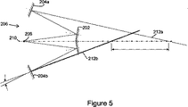
[0049] 本発明のさらなる実施形態が、図5に図示されている。集光器は、円錐形第一ミラー202及び第二ミラー204a、bを備え、これは円錐形ミラーを形成するように構成された1組の平面鏡領域を備える。第二円錐形ミラー204a、bには、放射源208からの放射を第一円錐形ミラー202に渡せるようにする開口206が設けられる。図5の上半分(つまり光軸210より上にある要素)は、特定の発散を有する放射ビーム212aを形成する第一構成の第二円錐形ミラー204aを示す。図5の下半分では、第二円錐形ミラー204bを備える平面鏡領域が傾斜しており(1つの平坦な平面鏡領域のみ図示)、これによって放射ビーム212bに異なる発散を提供する。平面鏡領域204bの傾斜は、例えば1つ又は複数の適切なアクチュエータを使用して達成することができる。
[0049] A further embodiment of the invention is illustrated in FIG. The concentrator comprises a conical
[0050] 第一円錐形ミラー202は、適切に配置された1組の平面鏡領域を備えることができる。これらの平面鏡領域は、第二円錐形ミラー204bの平面鏡領域を傾斜する代わりに(例えば1つ又は複数のアクチュエータを使用して)傾斜させることができる。あるいは、第一及び第二円錐形ミラー202、204a、bの平面鏡領域を、両方とも傾斜してよい。場合によっては、第一及び/又は第二円錐形ミラー202、204a、bは両方とも傾斜可能で、光軸に沿って平行移動可能でよい。
[0050] The first
[0051] さらなる構成では、ミラー領域は平坦ではなく、多少の湾曲を含む。湾曲は、例えば第一及び/又は第二円錐形ミラー202、204a、bの周囲に横方向に延在してよい。代替的又は追加的に、湾曲は例えば第一及び/又は第二ミラー202、204a、bに沿って延在してよい。
[0051] In a further configuration, the mirror region is not flat and includes some curvature. The curvature may e.g. extend laterally around the first and / or second conical mirrors 202, 204a, b. Alternatively or additionally, the curvature may extend, for example, along the first and / or
[0052] 図3に関して上述したイルミネータILは、図4及び図5に関して説明した本発明の実施形態とともに使用することができる。 [0052] The illuminator IL described above with respect to FIG. 3 may be used with the embodiments of the present invention described with respect to FIGS.
[0053] 本文ではICの製造におけるリソグラフィ装置の使用に特に言及しているが、本明細書で説明するリソグラフィ装置には他の用途もあることは言うまでもない。例えば、これは、集積光学装置、磁気ドメインメモリ用誘導及び検出パターン、フラットパネルディスプレイ、液晶ディスプレイ(LCD)、薄膜磁気ヘッドなどである。こうした代替的な用途に照らして、本明細書で「ウェーハ」又は「ダイ」という用語を使用している場合、それぞれ、「基板」又は「ターゲット部分」という、より一般的な用語と同義と見なしてよいことは、当業者に認識される。本明細書に述べている基板は、露光前又は露光後に、例えばトラック(通常はレジストの層を基板に塗布し、露光したレジストを現像するツール)、計測ツール及び/又は検査ツールで処理することができる。適宜、本明細書の開示は、以上及びその他の基板処理ツールに適用することができる。さらに、基板は、例えば多層ICを生成するために、複数回処理することができ、したがって本明細書で使用する基板という用語は、既に複数の処理済み層を含む基板も指すことができる。 [0053] Although the text specifically refers to the use of a lithographic apparatus in the manufacture of ICs, it will be appreciated that the lithographic apparatus described herein has other uses. For example, this is an integrated optical device, guidance and detection patterns for magnetic domain memory, flat panel displays, liquid crystal displays (LCDs), thin film magnetic heads, and the like. In light of these alternative applications, the use of the terms “wafer” or “die” herein are considered synonymous with the more general terms “substrate” or “target portion”, respectively. It will be appreciated by those skilled in the art. The substrate described herein may be processed before or after exposure, eg, with a track (usually a tool that applies a layer of resist to the substrate and develops the exposed resist), metrology tool, and / or inspection tool. Can do. Where appropriate, the disclosure herein may be applied to these and other substrate processing tools. In addition, the substrate can be processed multiple times, for example to produce a multi-layer IC, so the term substrate as used herein can also refer to a substrate that already contains multiple processed layers.
[0054] 以上の本発明の実施形態に関する説明では、UEV放射の使用に言及してきたが、他の波長の放射を使用してよいことが認識される。したがって、本明細書で使用する「放射」及び「ビーム」という用語は、適宜イオンビームあるいは電子ビームといったような粒子ビームのみならず、紫外線(UV)放射(例えば、365nm、355nm、248nm、193nm、157nm若しくは126nm、又はの波長を有する)及び極端紫外線光(EUV)放射(例えば、5nm〜20nmの範囲の波長を有する)を含むあらゆるタイプの電磁放射を網羅する。 [0054] While the above description of embodiments of the invention has referred to the use of UEV radiation, it will be appreciated that radiation of other wavelengths may be used. Thus, as used herein, the terms “radiation” and “beam” include not only particle beams such as ion beams or electron beams, but also ultraviolet (UV) radiation (eg, 365 nm, 355 nm, 248 nm, 193 nm, All types of electromagnetic radiation are encompassed, including 157 nm or 126 nm, or extreme ultraviolet light (EUV) radiation (eg having a wavelength in the range of 5 nm to 20 nm).
[0055] 「レンズ」という用語は、状況が許せば、屈折、反射、磁気、電磁気及び静電気光学部品を含む様々なタイプの光学部品のいずれか、又はその組合せを指す。 [0055] The term "lens" refers to any of various types of optical components, or combinations thereof, including refractive, reflective, magnetic, electromagnetic and electrostatic optical components, as the situation allows.
[0056] 上記の説明は例示的であり、限定的ではない。したがって、請求の範囲から逸脱することなく、記載されたような本発明を変更できることが当業者には明白である。 [0056] The descriptions above are intended to be illustrative, not limiting. Thus, it will be apparent to one skilled in the art that modifications may be made to the invention as described without departing from the scope of the claims set out below.
Claims (7)
反射性外面がある円錐形第一ミラーと、
反射性内面及び開口がある円錐形第二ミラーとを備え、
使用時に、放射エミッタからの放射が前記開口を通過し、前記第二円錐形ミラーに入射する前に前記第一円錐形ミラーに入射し、
前記光学装置が前記放射から放射ビームを形成し、
前記放射ビームの発散を調節するために、前記第一円錐形ミラーが前記第二円錐形ミラーに向かって及び前記第二円錐形ミラーから離れるように平行移動可能であるか、前記第二円錐形ミラーが前記第一円錐形ミラーに向かって及び前記第一円錐形ミラーから平行移動可能であり、
前記第一円錐形ミラーは、第1及び第2の要素を有し、前記放射ビームの発散を調節するために、前記第1の要素が前記第2の要素に向かって及び前記第2の要素から離れるようにさらに平行移動可能である、光学装置。An optical device,
A conical first mirror with a reflective outer surface;
A conical second mirror with a reflective inner surface and an aperture;
In use, radiation from a radiation emitter enters the first conical mirror before passing through the aperture and entering the second conical mirror;
The optical device forms a beam of radiation from the radiation;
In order to adjust the divergence of the radiation beam, the first conical mirror is translatable towards the second conical mirror and away from the second conical mirror, or the second conical shape mirror Ri translatable der and from said first conical mirror toward the first conical mirror,
The first conical mirror has first and second elements, wherein the first element is directed toward the second element and the second element to adjust the divergence of the radiation beam. An optical device that is further translatable away from the device.
前記光学装置によって形成された前記放射ビームを調整する照明システムと、
前記放射ビームの断面にパターンを与えて、パターン付き放射ビームを形成することができるパターニングデバイスを支持する支持体と、
前記パターン付き放射ビームを基板のターゲット部分に投影する投影システムと、
を備え、
前記第一円錐形ミラーは、第1及び第2の要素を有し、前記放射ビームの発散を調節するために、前記第1の要素が前記第2の要素に向かって及び前記第2の要素から離れるようにさらに平行移動可能である、リソグラフィ装置。An optical device comprising a conical first mirror with a reflective outer surface and a conical second mirror with a reflective inner surface and an aperture, wherein in use, radiation passes through the aperture, the second conical mirror The first conical mirror is incident on the first conical mirror before it enters the first conical mirror, and the optical device forms a radiation beam from the radiation and adjusts the divergence of the radiation beam. Can be translated towards and away from the second conical mirror, or so that the second conical mirror is towards and away from the first conical mirror An optical device capable of translation;
An illumination system for adjusting the radiation beam formed by the optical device;
A support that supports a patterning device capable of providing a pattern in a cross-section of the radiation beam to form a patterned radiation beam;
A projection system for projecting the patterned radiation beam onto a target portion of a substrate;
Equipped with a,
The first conical mirror has first and second elements, wherein the first element is directed toward the second element and the second element to adjust the divergence of the radiation beam. A lithographic apparatus that is further translatable away from the apparatus.
Applications Claiming Priority (3)
| Application Number | Priority Date | Filing Date | Title |
|---|---|---|---|
| US11/471,728 | 2006-06-21 | ||
| US11/471,728 US7817246B2 (en) | 2006-06-21 | 2006-06-21 | Optical apparatus |
| PCT/EP2007/005144 WO2007147498A1 (en) | 2006-06-21 | 2007-06-11 | Optical apparatus |
Publications (2)
| Publication Number | Publication Date |
|---|---|
| JP2009541977A JP2009541977A (en) | 2009-11-26 |
| JP5002009B2 true JP5002009B2 (en) | 2012-08-15 |
Family
ID=38561754
Family Applications (1)
| Application Number | Title | Priority Date | Filing Date |
|---|---|---|---|
| JP2009515735A Expired - Fee Related JP5002009B2 (en) | 2006-06-21 | 2007-06-11 | Optical device |
Country Status (5)
| Country | Link |
|---|---|
| US (1) | US7817246B2 (en) |
| JP (1) | JP5002009B2 (en) |
| KR (1) | KR20090018149A (en) |
| TW (1) | TWI374340B (en) |
| WO (1) | WO2007147498A1 (en) |
Families Citing this family (4)
| Publication number | Priority date | Publication date | Assignee | Title |
|---|---|---|---|---|
| KR20120045025A (en) * | 2009-08-14 | 2012-05-08 | 에이에스엠엘 네델란즈 비.브이. | Euv radiation system and lithographic apparatus |
| US10061201B2 (en) * | 2016-10-24 | 2018-08-28 | Hrl Laboratories, Llc | Bottom up apparatus design for formation of self-propagating photopolymer waveguides |
| US11934105B2 (en) * | 2017-04-19 | 2024-03-19 | Nikon Corporation | Optical objective for operation in EUV spectral region |
| CN116045828B (en) * | 2023-03-29 | 2023-10-20 | 睿励科学仪器(上海)有限公司 | Spectrum ellipsometry system and spectrum ellipsometry method |
Family Cites Families (38)
| Publication number | Priority date | Publication date | Assignee | Title |
|---|---|---|---|---|
| BE754893A (en) * | 1969-08-16 | 1971-02-15 | Philips Nv | OPTICAL REPRESENTATION SYSTEM INCLUDING A MIRROR SYSTEM CONSISTING OF A CONVEX SPHERICAL MIRROR AND A SPHERICAL MIRROR WITH AN OPENING |
| JPS6053848B2 (en) * | 1980-10-17 | 1985-11-27 | 松下電器産業株式会社 | Beam concentrator |
| US4812030A (en) * | 1985-01-03 | 1989-03-14 | The Boeing Company | Catoptric zoom optical device |
| EP0237041B1 (en) * | 1986-03-12 | 1993-08-18 | Matsushita Electric Industrial Co., Ltd. | Projection optical system for use in precise copy |
| US4988858A (en) * | 1986-11-12 | 1991-01-29 | The Boeing Company | Catoptric multispectral band imaging and detecting device |
| US4863253A (en) * | 1987-09-25 | 1989-09-05 | Spectra-Tech, Inc. | High magnification reflecting microscope objective having a dual magnification mode and zoom magnification capability |
| US4886348A (en) * | 1988-10-26 | 1989-12-12 | Westinghouse Electric Corp. | Total transmissibility optical system |
| US5136413A (en) * | 1990-11-05 | 1992-08-04 | Litel Instruments | Imaging and illumination system with aspherization and aberration correction by phase steps |
| US5212588A (en) * | 1991-04-09 | 1993-05-18 | The United States Of America As Represented By The United States Department Of Energy | Reflective optical imaging system for extreme ultraviolet wavelengths |
| JPH0547637A (en) * | 1991-08-19 | 1993-02-26 | Toshiba Corp | Light source device |
| JP3077920B2 (en) * | 1991-09-30 | 2000-08-21 | 日本電信電話株式会社 | Optical system evaluation apparatus and optical system evaluation method |
| JP3151260B2 (en) * | 1991-12-09 | 2001-04-03 | オリンパス光学工業株式会社 | Incident X-ray microscope |
| JPH05297278A (en) * | 1992-04-23 | 1993-11-12 | Shimadzu Corp | Optical device for irradiation with laser beam |
| JP2866267B2 (en) * | 1992-12-11 | 1999-03-08 | 三菱電機株式会社 | Optical drawing apparatus and optical drawing method for wafer substrate |
| US5510230A (en) * | 1994-10-20 | 1996-04-23 | At&T Corp. | Device fabrication using DUV/EUV pattern delineation |
| US6007963A (en) * | 1995-09-21 | 1999-12-28 | Sandia Corporation | Method for extreme ultraviolet lithography |
| US5737137A (en) * | 1996-04-01 | 1998-04-07 | The Regents Of The University Of California | Critical illumination condenser for x-ray lithography |
| JPH10213747A (en) * | 1997-01-30 | 1998-08-11 | Mitsubishi Electric Corp | Inverted telephotographic type catopric system |
| JP4238390B2 (en) | 1998-02-27 | 2009-03-18 | 株式会社ニコン | LIGHTING APPARATUS, EXPOSURE APPARATUS PROVIDED WITH THE ILLUMINATION APPARATUS, AND METHOD FOR MANUFACTURING SEMICONDUCTOR DEVICE USING THE EXPOSURE APPARATUS |
| EP0955641B1 (en) * | 1998-05-05 | 2004-04-28 | Carl Zeiss | Illumination system,particularly for deep ultraviolet lithography |
| US6225027B1 (en) * | 1998-08-06 | 2001-05-01 | Euv Llc | Extreme-UV lithography system |
| US6331710B1 (en) | 1998-12-02 | 2001-12-18 | Zhijiang Wang | Reflective optical systems for EUV lithography |
| JP2001066399A (en) * | 1999-08-27 | 2001-03-16 | Nikon Corp | Multilayer film reflecting mirror and exposure device or analyzer |
| US6560039B1 (en) * | 1999-09-28 | 2003-05-06 | Tropel Corporation | Double mirror catadioptric objective lens system with three optical surface multifunction component |
| JP2001332489A (en) * | 2000-03-13 | 2001-11-30 | Nikon Corp | Lighting optical system, projection aligner, and device- manufacturing method |
| DE10045265A1 (en) | 2000-09-13 | 2002-03-21 | Zeiss Carl | Device for focusing the radiation from a light source |
| JP2005038605A (en) * | 2002-02-12 | 2005-02-10 | Daisei Denki Kk | Lighting apparatus |
| US6771352B2 (en) * | 2002-03-18 | 2004-08-03 | Asml Netherlands B.V. | Lithographic apparatus and device manufacturing method |
| US6859259B2 (en) * | 2002-08-15 | 2005-02-22 | Asml Netherlands B.V. | Lithographic projection apparatus and reflector assembly for use therein |
| JP2004101404A (en) * | 2002-09-11 | 2004-04-02 | Shimadzu Corp | X-ray analysis system |
| JP2004343082A (en) * | 2003-04-17 | 2004-12-02 | Asml Netherlands Bv | Lithographic projection apparatus with condenser including concave face and convex face |
| US7781750B2 (en) * | 2003-08-27 | 2010-08-24 | Carl Zeiss Smt Ag | Oblique mirror-type normal-incidence collector system for light sources, particularly EUV plasma discharge sources |
| JP2005340319A (en) * | 2004-05-25 | 2005-12-08 | Nikon Corp | Light source device, lighting apparatus, exposure apparatus, exposure method, and method for adjustment |
| US7098466B2 (en) | 2004-06-30 | 2006-08-29 | Intel Corporation | Adjustable illumination source |
| US8134687B2 (en) | 2004-08-23 | 2012-03-13 | Carl Zeiss Smt Gmbh | Illumination system of a microlithographic exposure apparatus |
| US20060138349A1 (en) * | 2004-12-27 | 2006-06-29 | Asml Netherlands B.V. | Lithographic apparatus and device manufacturing method |
| US7331676B2 (en) | 2005-02-09 | 2008-02-19 | Coherent, Inc. | Apparatus for projecting a reduced image of a photomask using a schwarzschild objective |
| JP2007047704A (en) * | 2005-08-12 | 2007-02-22 | Y E Data Inc | Light source for exposure device |
-
2006
- 2006-06-21 US US11/471,728 patent/US7817246B2/en not_active Expired - Fee Related
-
2007
- 2007-06-11 WO PCT/EP2007/005144 patent/WO2007147498A1/en active Application Filing
- 2007-06-11 KR KR1020087031005A patent/KR20090018149A/en active Search and Examination
- 2007-06-11 JP JP2009515735A patent/JP5002009B2/en not_active Expired - Fee Related
- 2007-06-15 TW TW096121661A patent/TWI374340B/en not_active IP Right Cessation
Also Published As
| Publication number | Publication date |
|---|---|
| TW200807181A (en) | 2008-02-01 |
| US7817246B2 (en) | 2010-10-19 |
| KR20090018149A (en) | 2009-02-19 |
| US20070296943A1 (en) | 2007-12-27 |
| WO2007147498A1 (en) | 2007-12-27 |
| JP2009541977A (en) | 2009-11-26 |
| TWI374340B (en) | 2012-10-11 |
Similar Documents
| Publication | Publication Date | Title |
|---|---|---|
| JP4313328B2 (en) | Lithographic apparatus, device manufacturing method and variable attenuator | |
| JP4004461B2 (en) | Device manufacturing method, computer program, and lithographic projection apparatus | |
| JP5335108B2 (en) | Illumination system, lithographic apparatus and method | |
| US9134629B2 (en) | Illumination system, lithographic apparatus and method of forming an illumination mode | |
| JP4339840B2 (en) | Lithographic apparatus | |
| JP4429267B2 (en) | Lithographic apparatus and device manufacturing method | |
| JP2010524231A (en) | Illumination system for illuminating a patterning device and method of manufacturing an illumination system | |
| JP4303192B2 (en) | Lithographic apparatus and device manufacturing method | |
| JP5002009B2 (en) | Optical device | |
| JP4999827B2 (en) | Lithographic apparatus | |
| JP4838295B2 (en) | Pulse corrector, lithography equipment | |
| US10156791B2 (en) | Lithographic apparatus and method | |
| JP2007194600A (en) | Lithography device, and device manufacturing method | |
| JP3986492B2 (en) | Lithographic apparatus and method for determining beam size and divergence | |
| JP2007043168A (en) | Lithography equipment and method for manufacturing device | |
| JP5033175B2 (en) | Lithographic apparatus and patterning device | |
| JP4376227B2 (en) | Projection apparatus for lithographic apparatus | |
| US7177059B2 (en) | Device and method for manipulation and routing of a metrology beam | |
| KR100700369B1 (en) | Lithographic apparatus, illumination system and method for providing a projection beam of euv radiation | |
| JP4741560B2 (en) | Lithographic apparatus | |
| JP4777312B2 (en) | Particle detection system and lithographic apparatus comprising such a particle detection system | |
| JP2009111361A (en) | Lithographic apparatus, and method | |
| EP1455204A1 (en) | Device and method for manipulation and routing of a metrology beam |
Legal Events
| Date | Code | Title | Description |
|---|---|---|---|
| A977 | Report on retrieval |
Free format text: JAPANESE INTERMEDIATE CODE: A971007 Effective date: 20110928 |
|
| A131 | Notification of reasons for refusal |
Free format text: JAPANESE INTERMEDIATE CODE: A131 Effective date: 20111004 |
|
| A601 | Written request for extension of time |
Free format text: JAPANESE INTERMEDIATE CODE: A601 Effective date: 20111226 |
|
| A602 | Written permission of extension of time |
Free format text: JAPANESE INTERMEDIATE CODE: A602 Effective date: 20120106 |
|
| A521 | Request for written amendment filed |
Free format text: JAPANESE INTERMEDIATE CODE: A523 Effective date: 20120402 |
|
| TRDD | Decision of grant or rejection written | ||
| A01 | Written decision to grant a patent or to grant a registration (utility model) |
Free format text: JAPANESE INTERMEDIATE CODE: A01 Effective date: 20120420 |
|
| A01 | Written decision to grant a patent or to grant a registration (utility model) |
Free format text: JAPANESE INTERMEDIATE CODE: A01 |
|
| A61 | First payment of annual fees (during grant procedure) |
Free format text: JAPANESE INTERMEDIATE CODE: A61 Effective date: 20120518 |
|
| R150 | Certificate of patent or registration of utility model |
Free format text: JAPANESE INTERMEDIATE CODE: R150 |
|
| FPAY | Renewal fee payment (event date is renewal date of database) |
Free format text: PAYMENT UNTIL: 20150525 Year of fee payment: 3 |
|
| LAPS | Cancellation because of no payment of annual fees |