JP4993003B2 - Method of adjusting illumination optical device and exposure method - Google Patents
Method of adjusting illumination optical device and exposure method Download PDFInfo
- Publication number
- JP4993003B2 JP4993003B2 JP2010155578A JP2010155578A JP4993003B2 JP 4993003 B2 JP4993003 B2 JP 4993003B2 JP 2010155578 A JP2010155578 A JP 2010155578A JP 2010155578 A JP2010155578 A JP 2010155578A JP 4993003 B2 JP4993003 B2 JP 4993003B2
- Authority
- JP
- Japan
- Prior art keywords
- distribution
- adjustment
- transmittance
- irradiated surface
- reflectance
- Prior art date
- Legal status (The legal status is an assumption and is not a legal conclusion. Google has not performed a legal analysis and makes no representation as to the accuracy of the status listed.)
- Expired - Fee Related
Links
Images


Landscapes
- Exposure Of Semiconductors, Excluding Electron Or Ion Beam Exposure (AREA)
- Optical Elements Other Than Lenses (AREA)
- Exposure And Positioning Against Photoresist Photosensitive Materials (AREA)
Description
本発明は、照明光学装置の調整方法、露光装置、および露光方法に関し、特に半導体素子、撮像素子、液晶表示素子、薄膜磁気ヘッド等のマイクロデバイスをリソグラフィー工程で製造するための露光装置に好適な照明光学装置の調整方法に関するものである。 The present invention relates to an illumination optical apparatus adjustment method, exposure apparatus, and exposure method, and is particularly suitable for an exposure apparatus for manufacturing microdevices such as semiconductor elements, image sensors, liquid crystal display elements, and thin film magnetic heads in a lithography process. The present invention relates to a method for adjusting an illumination optical device.
この種の典型的な露光装置においては、光源から射出された光束が、オプティカルインテグレータとしてのフライアイレンズ(またはマイクロレンズアレイ)を介して、多数の光源からなる実質的な面光源としての二次光源を形成する。二次光源からの光束は、フライアイレンズの後側焦点面の近傍に配置された開口絞りを介して制限された後、コンデンサーレンズに入射する。 In a typical exposure apparatus of this type, a light beam emitted from a light source passes through a fly-eye lens (or microlens array) as an optical integrator, and a secondary light source as a substantial surface light source composed of a number of light sources. Form a light source. The light beam from the secondary light source is limited through an aperture stop disposed in the vicinity of the rear focal plane of the fly-eye lens, and then enters the condenser lens.
コンデンサーレンズにより集光された光束は、所定のパターンが形成されたマスクを重畳的に照明する。マスクのパターンを透過した光は、投影光学系を介してウェハ上に結像する。こうして、感光性基板としてのウェハ上には、マスクパターンが投影露光(転写)される。なお、マスクに形成されたパターンは高集積化されており、この微細パターンをウェハ上に正確に転写するにはウェハ上において均一な照度分布を得ることが不可欠である。 The light beam condensed by the condenser lens illuminates the mask on which a predetermined pattern is formed in a superimposed manner. The light transmitted through the mask pattern forms an image on the wafer via the projection optical system. Thus, the mask pattern is projected and exposed (transferred) onto the wafer as the photosensitive substrate. The pattern formed on the mask is highly integrated, and it is essential to obtain a uniform illuminance distribution on the wafer in order to accurately transfer this fine pattern onto the wafer.
また、フライアイレンズの後側焦点面に円形状の二次光源を形成し、その大きさを変化させて照明のコヒーレンシィσ(σ値=開口絞り径/投影光学系の瞳径、あるいはσ値=照明光学系の射出側開口数/投影光学系の入射側開口数)を変化させる技術が注目されている。また、フライアイレンズの後側焦点面に輪帯状や4極状の二次光源を形成し、投影光学系の焦点深度や解像力を向上させる技術が注目されている。 Further, a circular secondary light source is formed on the rear focal plane of the fly-eye lens, and its size is changed to change the illumination coherency σ (σ value = aperture aperture diameter / projection optical system pupil diameter, or σ Attention has been focused on a technique of changing the value = the exit numerical aperture of the illumination optical system / the incident numerical aperture of the projection optical system. Further, attention has been focused on a technique for forming an annular or quadrupolar secondary light source on the rear focal plane of the fly-eye lens to improve the depth of focus and resolution of the projection optical system.
この場合、マスクの微細パターンをウェハ上に忠実に転写するには、フライアイレンズの後側焦点面に形成される二次光源の光強度分布すなわち照明瞳面に形成される所定の輝度分布を有する瞳輝度分布を所望の形状に調整するだけでなく、最終的な被照射面としてのウェハ上の各点に関する瞳輝度分布をそれぞれほぼ均一に調整する必要がある。ウェハ上の各点での瞳輝度分布の均一性にばらつきがあると、ウェハ上の位置毎にパターンの線幅がばらついて、マスクの微細パターンを露光領域の全体に亘って所望の線幅でウェハ上に忠実に転写することができない。 In this case, in order to faithfully transfer the fine pattern of the mask onto the wafer, a light intensity distribution of the secondary light source formed on the rear focal plane of the fly-eye lens, that is, a predetermined luminance distribution formed on the illumination pupil plane is used. In addition to adjusting the pupil brightness distribution to a desired shape, it is necessary to adjust the pupil brightness distribution for each point on the wafer as the final irradiated surface to be approximately uniform. If there is a variation in the uniformity of the pupil luminance distribution at each point on the wafer, the line width of the pattern varies from position to position on the wafer, and the fine pattern of the mask has the desired line width over the entire exposure area. It cannot be faithfully transferred onto the wafer.
本発明は、前述の課題に鑑みてなされたものであり、被照射面での照度分布をほぼ均一に維持または調整しつつ、被照射面上の各点での瞳輝度分布をそれぞれほぼ均一に調整することのできる照明光学装置の調整方法を提供することを目的とする。また、本発明は、被照射面での照度分布をほぼ均一に維持可能または調整可能で且つ被照射面上の各点での瞳輝度分布をほぼ均一に調整可能な照明光学装置の調整方法を利用して、マスクの微細パターンを露光領域の全体に亘って所望の線幅で感光性基板上に忠実に転写することのできる露光装置および露光方法を提供することを目的とする。 The present invention has been made in view of the above-described problems. While maintaining or adjusting the illuminance distribution on the irradiated surface substantially uniformly, the pupil luminance distribution at each point on the irradiated surface is substantially uniform. It is an object of the present invention to provide a method for adjusting an illumination optical device that can be adjusted. The present invention also provides a method for adjusting an illumination optical device that can maintain or adjust the illuminance distribution on the irradiated surface substantially uniformly and can adjust the pupil luminance distribution at each point on the irradiated surface substantially uniformly. It is an object of the present invention to provide an exposure apparatus and an exposure method capable of faithfully transferring a fine pattern of a mask onto a photosensitive substrate with a desired line width over the entire exposure region.
前記課題を解決するために、本発明の第1形態では、光源からの光束に基づいて照明瞳面に所定の輝度分布を有する瞳輝度分布を形成し、該瞳輝度分布からの光束で被照射面を照明する照明光学装置の調整方法において、
前記被照射面上の複数点に関する瞳輝度分布を得る瞳輝度分布獲得工程と、
前記複数点に関する瞳輝度分布をそれぞれ独立に調整するために、前記照明光学装置の光路中の複数の位置での所要の透過率分布または反射率分布を決定する分布決定工程と、
前記所要の透過率分布または反射率分布を有する複数の調整膜をそれぞれ形成して前記複数の位置に配置する調整工程とを含むことを特徴とする調整方法を提供する。
In order to solve the above-mentioned problem, in the first embodiment of the present invention, a pupil luminance distribution having a predetermined luminance distribution is formed on the illumination pupil plane based on the luminous flux from the light source, and irradiation is performed with the luminous flux from the pupil luminance distribution. In an adjustment method of an illumination optical device that illuminates a surface,
A pupil luminance distribution acquisition step of obtaining a pupil luminance distribution for a plurality of points on the irradiated surface;
A distribution determining step for determining a required transmittance distribution or reflectance distribution at a plurality of positions in the optical path of the illumination optical device in order to independently adjust pupil luminance distributions regarding the plurality of points;
And an adjusting step of forming a plurality of adjusting films each having the required transmittance distribution or reflectance distribution and arranging the adjusting films at the plurality of positions.
本発明の第2形態では、第1形態の調整方法により調整された照明光学装置を備え、前記照明光学装置で照明されたマスクのパターンを感光性基板上に露光することを特徴とする露光装置を提供する。 According to a second aspect of the present invention, there is provided an exposure apparatus comprising the illumination optical apparatus adjusted by the adjustment method according to the first aspect, and exposing a mask pattern illuminated by the illumination optical apparatus onto a photosensitive substrate. I will provide a.
本発明の第3形態では、第1形態の調整方法により調整された照明光学装置を用いてマスクを照明する照明工程と、前記マスクのパターンを感光性基板上に露光する露光工程とを含むことを特徴とする露光方法を提供する。 In the third embodiment of the present invention, the method includes an illumination step of illuminating the mask using the illumination optical device adjusted by the adjustment method of the first embodiment, and an exposure step of exposing the pattern of the mask on a photosensitive substrate. An exposure method is provided.
本発明の照明光学装置の調整方法では、たとえば所定の透過率分布を有する複数の調整膜の作用により、被照射面での照度分布をほぼ均一に維持または調整しつつ、被照射面上の各点での瞳輝度分布をそれぞれほぼ均一に調整することができる。 In the adjustment method of the illumination optical device according to the present invention, for example, the operation of a plurality of adjustment films having a predetermined transmittance distribution allows each illumination on the irradiated surface to be maintained or adjusted while maintaining or adjusting the illuminance distribution almost uniformly. The pupil luminance distribution at the points can be adjusted substantially uniformly.
また、本発明の露光装置および露光方法では、被照射面での照度分布をほぼ均一に維持可能または調整可能で且つ被照射面上の各点での瞳輝度分布をほぼ均一に調整可能な照明光学装置の調整方法を利用しているので、マスクの微細パターンを露光領域の全体に亘って所望の線幅で感光性基板上に忠実に転写することができ、ひいては高精度で良好なデバイスを製造することができる。 In the exposure apparatus and exposure method of the present invention, the illumination intensity distribution on the irradiated surface can be maintained or adjusted substantially uniformly, and the pupil luminance distribution at each point on the irradiated surface can be adjusted substantially uniformly. Since the adjustment method of the optical device is used, the fine pattern of the mask can be faithfully transferred onto the photosensitive substrate with a desired line width over the entire exposure region, and thus a high-precision and good device can be obtained. Can be manufactured.
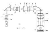
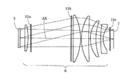
本発明の実施形態を、添付図面に基づいて説明する。図1は、本発明の実施形態にかかる露光装置の全体構成を概略的に示す図である。図1において、感光性基板であるウェハWの法線方向に沿ってZ軸を、ウェハWの面内において図1の紙面に平行な方向にY軸を、ウェハWの面内において図1の紙面に垂直な方向にX軸をそれぞれ設定している。なお、図1では、照明光学装置が通常の円形照明を行うように設定されている。 Embodiments of the present invention will be described with reference to the accompanying drawings. FIG. 1 is a view schematically showing the overall configuration of an exposure apparatus according to an embodiment of the present invention. In FIG. 1, the Z axis along the normal direction of the wafer W, which is a photosensitive substrate, the Y axis in the direction parallel to the plane of FIG. 1 in the plane of the wafer W, and the plane of the wafer W in FIG. The X axis is set in the direction perpendicular to the paper surface. In FIG. 1, the illumination optical device is set to perform normal circular illumination.
図1を参照すると、本実施形態の露光装置は、露光光(照明光)を供給するための光源1を備えている。光源1として、たとえば248nmの波長の光を供給するKrFエキシマレーザ光源や193nmの波長の光を供給するArFエキシマレーザ光源などを用いることができる。光源1から+Z方向に沿って射出されたほぼ平行な光束は、X方向に沿って細長く延びた矩形状の断面を有し、一対のレンズ2aおよび2bからなるビームエキスパンダー2に入射する。
Referring to FIG. 1, the exposure apparatus of this embodiment includes a
各レンズ2aおよび2bは、図1の紙面内(YZ平面内)において負の屈折力および正の屈折力をそれぞれ有する。したがって、ビームエキスパンダー2に入射した光束は、図1の紙面内において拡大され、所定の矩形状の断面を有する光束に整形される。整形光学系としてのビームエキスパンダー2を介したほぼ平行な光束は、光路折り曲げミラーで+Y方向に偏向された後、円形照明用の回折光学素子3を介して、ズームレンズ4に入射する。ズームレンズ4の後側焦点面の近傍には、マイクロフライアイレンズ5の入射面が位置決めされている。
Each
一般に、回折光学素子は、基板に露光光(照明光)の波長程度のピッチを有する段差を形成することによって構成され、入射ビームを所望の角度に回折する作用を有する。具体的には、回折光学素子3は、光軸AXに沿って入射した矩形状の平行光束を、円形状の断面を有する発散光束に変換する。回折光学素子3は、照明光路に対して挿脱自在に構成され、且つ輪帯照明用の回折光学素子や4極照明用の回折光学素子と切り換え可能に構成されている。
In general, a diffractive optical element is formed by forming a step having a pitch of the wavelength of exposure light (illumination light) on a substrate, and has a function of diffracting an incident beam to a desired angle. Specifically, the diffractive
マイクロフライアイレンズ5は、縦横に且つ稠密に配列された多数の微小レンズ(光学要素)からなる光学部材である。一般に、マイクロフライアイレンズは、たとえば平行平面ガラス板にMEMS技術(リソグラフィー+エッチング等)を応用して多数の微小光学面を同時形成することによって構成される。こうして、回折光学素子3を介した光束は、ズームレンズ4を介して、波面分割型のオプティカルインテグレータとしてのマイクロフライアイレンズ5の入射面に、たとえば光軸AXを中心とする円形状の照野を形成する。
The micro fly's eye lens 5 is an optical member composed of a large number of microlenses (optical elements) arranged vertically and horizontally and densely. In general, a micro fly's eye lens is configured by simultaneously forming a large number of micro optical surfaces on a parallel flat glass plate by applying MEMS technology (lithography + etching or the like). Thus, the light beam that has passed through the diffractive
ここで、形成される円形状の照野の大きさ(すなわちその直径)は、ズームレンズ4の焦点距離に依存して変化する。マイクロフライアイレンズ5に入射した光束は多数の微小レンズにより二次元的に分割され、光束が入射した各微小レンズの後側焦点面には光源がそれぞれ形成される。こうして、マイクロフライアイレンズ5の後側焦点面には、マイクロフライアイレンズ5への入射光束によって形成される円形状の照野とほぼ同じ光強度分布を有する円形状の実質的な面光源(以下、「二次光源」という)が形成される。 Here, the size of the circular illumination field formed (that is, its diameter) changes depending on the focal length of the zoom lens 4. The light beam incident on the micro fly's eye lens 5 is two-dimensionally divided by a large number of minute lenses, and a light source is formed on the rear focal plane of each minute lens on which the light beam is incident. Thus, on the rear focal plane of the micro fly's eye lens 5, a circular substantial surface light source having substantially the same light intensity distribution as the circular illumination field formed by the light beam incident on the micro fly's eye lens 5 ( (Hereinafter referred to as “secondary light source”).
マイクロフライアイレンズ5の後側焦点面に形成された円形状の二次光源からの光束は、コンデンサー光学系6の集光作用を受けた後、マスクM(ひいてはウェハW)と光学的に共役な面に配置されたマスクブラインド7を重畳的に照明する。こうして、マスクブラインド7には、マイクロフライアイレンズ5を構成する各微小レンズの形状と相似な矩形状の照野が形成される。なお、マスクブラインド7の前側(光源側)には第1補正フィルター8が配置され、マスクブラインド7の後側(マスク側)には第2補正フィルター9が配置されている。第1補正フィルター8および第2補正フィルター9の構成および作用については後述する。
The light beam from the circular secondary light source formed on the rear focal plane of the micro fly's eye lens 5 is optically conjugate with the mask M (and thus the wafer W) after receiving the light condensing action of the condenser
マスクブラインド7の矩形状の開口部(光透過部)を介した光束は、結像光学系10の集光作用を受け、光路折り曲げミラーで−Z方向に偏向された後、所定のパターンが形成されたマスクMを重畳的に照明する。このように、結像光学系10は、マスクブラインド7の矩形状の開口部の像を、マスクステージMSにより支持されたマスクM上に形成することになる。すなわち、マスクブラインド7は、マスクM(ひいてはウェハW)上に形成される照明領域を規定するための視野絞りを構成している。
The light beam that has passed through the rectangular opening (light transmission portion) of the
マスクMのパターンを透過した光束は、投影光学系PLを介して、感光性基板であるウェハW上にマスクパターンの像を形成する。すなわち、ウェハステージWSにより支持されたウェハW上には、マスクM上での矩形状の照明領域に対応するように矩形状の領域にパターン像が形成される。こうして、投影光学系PLの光軸AXと直交する平面(XY平面)内においてウェハWを二次元的に駆動制御しながら一括露光またはスキャン露光を行うことにより、ウェハWの各露光領域にはマスクMのパターンが逐次露光される。 The light beam that has passed through the pattern of the mask M forms an image of the mask pattern on the wafer W, which is a photosensitive substrate, via the projection optical system PL. That is, on the wafer W supported by the wafer stage WS, a pattern image is formed in a rectangular area so as to correspond to the rectangular illumination area on the mask M. Thus, by performing batch exposure or scan exposure while driving and controlling the wafer W two-dimensionally in a plane (XY plane) orthogonal to the optical axis AX of the projection optical system PL, each exposure region of the wafer W is masked. M patterns are sequentially exposed.
なお、回折光学素子3に代えて輪帯照明用の回折光学素子を照明光路中に設定することによって輪帯照明を行うことができる。輪帯照明用の回折光学素子は、光軸AXに沿って入射した矩形状の平行光束を、輪帯状の断面を有する発散光束に変換する。したがって、輪帯照明用の回折光学素子を介した光束は、マイクロフライアイレンズ5の入射面に、たとえば光軸AXを中心とした輪帯状の照野を形成する。その結果、マイクロフライアイレンズ5の後側焦点面にも、その入射面に形成された輪帯状の照野とほぼ同じ光強度分布を有する輪帯状の二次光源が形成される。
Note that annular illumination can be performed by setting a diffractive optical element for annular illumination in the illumination optical path instead of the diffractive
また、回折光学素子3に代えて4極照明用(一般には、2極、8極などを含む複数極照明用)の回折光学素子を照明光路中に設定することによって4極照明(一般には複数極照明)を行うことができる。4極照明用の回折光学素子は、光軸AXに沿って入射した矩形状の平行光束を、4極状の断面を有する発散光束に変換する。したがって、4極照明用の回折光学素子を介した光束は、マイクロフライアイレンズ5の入射面に、たとえば光軸AXを中心とした4極状の照野を形成する。その結果、マイクロフライアイレンズ5の後側焦点面にも、その入射面に形成された4極状の照野とほぼ同じ光強度分布を有する4極状の二次光源が形成される。
Further, instead of the diffractive
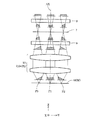
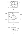
図2は、本実施形態における一対の補正フィルターの構成および作用を模式的に示す図である。本実施形態では、図2に示すように、マスクブラインド7の前側(光源側)に第1補正フィルター8が配置され、マスクブラインド7の後側(マスク側)に第2補正フィルター9が配置されている。第1補正フィルター8および第2補正フィルター9はともに平行平面板の形態を有し、入射位置に応じて透過率の異なる透過率分布を有する。すなわち、たとえば第1補正フィルター8のマスクブラインド7側の光学面および第2補正フィルター9のマスクブラインド7側の光学面には、クロムや酸化クロム等からなる遮光性ドットの濃密パターンが調整膜として形成されている。
FIG. 2 is a diagram schematically illustrating the configuration and operation of a pair of correction filters in the present embodiment. In the present embodiment, as shown in FIG. 2, the first correction filter 8 is disposed on the front side (light source side) of the
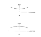
具体的に、第1補正フィルター8は、図3(a)に示すように、たとえばY方向に沿って有効領域の中心において透過率が最も低く且つ中心からの距離の二次関数にしたがって透過率が周辺に向かって単調に増大するような二次の凹状パターンの透過率分布を有する。一方、第2補正フィルター9は、図3(b)に示すように、たとえばY方向に沿って有効領域の中心において透過率が最も高く且つ中心からの距離の二次関数にしたがって透過率が周辺に向かって単調に減少するような二次の凸状パターンの透過率分布を有する。
Specifically, as shown in FIG. 3A, the first correction filter 8 has the lowest transmittance at the center of the effective region, for example, along the Y direction, and the transmittance according to a quadratic function of the distance from the center. Has a transmittance distribution of a secondary concave pattern that monotonously increases toward the periphery. On the other hand, as shown in FIG. 3B, the
そして、第1補正フィルター8では有効領域の周辺における透過率の最大値と中心における透過率の最小値との差が例えば4%に設定され、第2補正フィルター9では有効領域の周辺における透過率の最小値と中心における透過率の最大値との差が例えば4%に設定されている。すなわち、第1補正フィルター8は二次の4%凹状パターンの透過率分布を有し、第2補正フィルター9は二次の4%凸状パターンの透過率分布を有する。その結果、第1補正フィルター8と第2補正フィルター9とは相補的な透過率分布を有することになる。
In the first correction filter 8, the difference between the maximum value of the transmittance around the effective region and the minimum value of the transmittance in the center is set to 4%, for example, and in the
また、本実施形態では、第1補正フィルター8(厳密にはその調整膜であるマスク側の光学面)とマスクブラインド7との距離と、第2補正フィルター9(厳密にはその調整膜である光源側の光学面)とマスクブラインド7との距離とが互いに等しくなるように設定されている。ここで、被照射面としてのマスクM(または最終的な被照射面としてのウェハW)上において光軸AXと交わる中心点P1に達する光線、中心点P1から+Y方向に所定距離だけ離れた点P2に達する光線、および中心点P1から−Y方向に同じ所定距離だけ離れた点P3に達する光線に着目する。
In the present embodiment, the distance between the first correction filter 8 (strictly, the optical surface on the mask side that is the adjustment film) and the
そして、第1補正フィルター8および第2補正フィルター9が介在しない状態では、図2において第1補正フィルター8よりも上側に斜線部で示すように、中心点P1に関する瞳輝度分布、点P2に関する瞳輝度分布、および点P3に関する瞳輝度分布がともに均一であるものとする。なお、被照射面上のある点に関する瞳輝度分布が均一であるということは、当該点に達する光線が照明瞳面(たとえばマイクロフライアイレンズ5の後側焦点面)に形成する光強度分布が均一であることに他ならない。
In the state where the first correction filter 8 and the
ここで、二次の4%凹状パターンの透過率分布を有する第1補正フィルター8だけが介在すると、第1補正フィルター8の作用により、図2において第1補正フィルター8とマスクブラインド7との間およびマスクブラインド7と第2補正フィルター9との間に斜線部で示すように、中心点P1に関する瞳輝度分布が均一なパターンから凹状パターンに変化し、点P2に関する瞳輝度分布が均一なパターンから傾斜パターンに変化し、点P3に関する瞳輝度分布が均一なパターンから点P2の傾斜パターンとは傾斜方向が逆の傾斜パターンに変化する。
Here, if only the first correction filter 8 having the transmittance distribution of the secondary 4% concave pattern is interposed, the first correction filter 8 causes the first correction filter 8 and the
さらに、第1補正フィルター8に加えて二次の4%凸状パターンの透過率分布を有する第2補正フィルター9も介在すると、第2補正フィルター9の作用により、図2において第2補正フィルター9と結像光学系10(または結像光学系10+投影光学系PL)との間および結像光学系10(または結像光学系10+投影光学系PL)とマスクM(またはウェハW)との間に斜線部で示すように、中心点P1に関する瞳輝度分布が凹状パターンから均一なパターンに戻り、点P2および点P3に関する瞳輝度分布の傾斜パターンの傾斜の度合いがさらに助長された傾斜パターンに変化する。
Further, when a
換言すれば、第1補正フィルター8と第2補正フィルター9との協働作用により、中心点P1(およびP1と同じY座標を有する点)に関する均一な瞳輝度分布が変化することなく、点P2(およびP2と同じY座標を有する点)に関する均一な瞳輝度分布が線形的な傾斜パターンに変化し、点P3(およびP3と同じY座標を有する点)に関する均一な瞳輝度分布が点P2の傾斜パターンとは傾斜方向が逆で傾斜の度合いが等しい線形的な傾斜パターンに変化する。なお、点P2および点P3に関する瞳輝度分布の線形的な傾斜調整の度合いは、点P2および点P3の中心点P1からのY方向に沿った距離に依存する。
In other words, due to the cooperative action of the first correction filter 8 and the
すなわち、中心点P1からY方向に沿って離れるほど、その点に関する瞳輝度分布の線形的な傾斜調整の度合いは大きくなる。また、図2を参照すると明らかであるが、被照射面上の各点に達する光線が第1補正フィルター8および第2補正フィルター9をそれぞれ通過する領域(以下、「パーシャル領域」という)の大きさは、第1補正フィルター8および第2補正フィルター9がマスクブラインド7から離れるほど大きくなり、各点に関する瞳輝度分布の線形的な傾斜調整の度合いも大きくなる。もちろん、第1補正フィルター8および第2補正フィルター9の透過率分布の変化の度合い(上述の例では4%)をさらに大きく設定すると、各点に関する瞳輝度分布の線形的な傾斜調整の度合いも大きくなる。
That is, as the distance from the center point P1 in the Y direction increases, the degree of linear inclination adjustment of the pupil luminance distribution related to the point increases. In addition, as is apparent with reference to FIG. 2, the size of a region (hereinafter referred to as “partial region”) through which light rays reaching each point on the irradiated surface pass through the first correction filter 8 and the
また、上述したように、本実施形態では、第1補正フィルター8と第2補正フィルター9とが相補的な透過率分布を有し、第1補正フィルター8と第2補正フィルター9とがマスクブラインド7を挟んで等しい距離に設定されているので、被照射面上の各点に関するパーシャル領域の位置および大きさは第1補正フィルター8と第2補正フィルター9とでほぼ一致する。その結果、第1補正フィルター8と第2補正フィルター9との協働作用により、被照射面上の各点に関する瞳輝度分布は点毎にそれぞれ調整されるが、被照射面上の照度分布は実質的に変化することなくほぼ均一に維持される。
As described above, in the present embodiment, the first correction filter 8 and the
以上のように、本実施形態では、第1補正フィルター8と第2補正フィルター9とが、被照射面(M,W)上の各点に関する瞳輝度分布をそれぞれ独立的に調整するための調整手段を構成している。その結果、本実施形態の露光装置では、被照射面(M,W)での照度分布をほぼ均一に維持しつつ、被照射面上の各点での瞳輝度分布をそれぞれほぼ均一に調整することができるので、マスクMの微細パターンを露光領域の全体に亘って所望の線幅でウェハW上に忠実に転写することができる。
As described above, in the present embodiment, the first correction filter 8 and the
なお、上述の説明では、第1補正フィルター8と第2補正フィルター9とがマスクブラインド7を挟んで等しい距離に設定されているが、最終的な被照射面であるウェハWと光学的に共役な共役面を挟んで等しい距離に、具体的には例えばマスクMを挟んで等しい距離に設定しても上述の実施形態と同様の効果が得られる。また、上述の説明では、第1補正フィルター8が二次の凹状パターンの透過率分布を有し且つ第2補正フィルター9が二次の凸状パターンの透過率分布を有するが、第1補正フィルター8が二次の凸状パターンの透過率分布を有し且つ第2補正フィルター9が二次の凹状パターンの透過率分布を有する場合も上述の実施形態と同様の効果が得られる。
In the above description, the first correction filter 8 and the
また、上述の説明では、第1補正フィルター8および第2補正フィルター9が二次のパターンの透過率分布を有するが、これに限定されることなく、第1補正フィルター8および第2補正フィルター9に付与する透過率分布のパターンについては様々な変形例が可能である。具体的に、たとえば第1補正フィルター8が、図4(a)に示すように、たとえば有効領域の中心からのY方向に沿った距離の四次関数にしたがって中心から周辺に向かって透過率が一旦増大した後に減少するような四次のM字状パターンの透過率分布を有する変形例も可能である。
In the above description, the first correction filter 8 and the
この変形例では、第2補正フィルター9は、図4(b)に示すように、有効領域の中心からのY方向に沿った距離の四次関数にしたがって中心から周辺に向かって透過率が一旦減少した後に増大するような四次のW字状パターンの透過率分布を有することになる。この場合、第1補正フィルター8の透過率分布と第2補正フィルター9の透過率分布とを相補的に設定すれば、上述の実施形態と同様の効果が得られる。ただし、第1補正フィルター8および第2補正フィルター9が四次のパターンの透過率分布を有するため、線形的な傾斜調整ではなく三次関数的な傾斜調整効果が得られる。なお、第1補正フィルター8および第2補正フィルター9のパターンの透過率分布は四次以上であってもよい。
In this modification, as shown in FIG. 4B, the
また、上述の説明では、第1補正フィルター8および第2補正フィルター9にY方向に沿った一次元の透過率分布を付与しているが、一次元の透過率分布の変化方向については様々な変形例が可能である。また、第1補正フィルター8および第2補正フィルター9に二次元的な透過率分布を付与することもできる。また、第1補正フィルター8および第2補正フィルター9に付与すべき透過率分布を他の適当な関数にしたがって規定することもできる。一例として、たとえば後述するツェルニケ多項式を用いて第1補正フィルター8および第2補正フィルター9の透過率分布を規定することにより、被照射面上の各点に関する瞳輝度分布を多様な形態にしたがって点毎にそれぞれ調整することが可能になる。
In the above description, the first correction filter 8 and the
ところで、上述の実施形態において、クロムドットのような遮光性ドットの濃密パターンを用いて第1補正フィルター8および第2補正フィルター9に透過率分布を付与する場合、各ドットのウェハWへの転写および各ドットにおける回折の影響を評価して、各ドットの大きさや、第1補正フィルター8および第2補正フィルター9とマスクブラインド7との距離などを設定する必要がある。また、上述の説明では、遮光性ドットの濃密パターンを用いて第1補正フィルター8および第2補正フィルター9に透過率分布を付与しているが、これに限定されることなく、調整膜としての薄膜の厚みを制御することにより連続的に変化する透過率分布を付与することもできる。
By the way, in the above-described embodiment, when a transmittance distribution is given to the first correction filter 8 and the
なお、上述の実施形態では、第1補正フィルター8の透過率分布と第2補正フィルター9の透過率分布とが相補的に設定されているが、これに限定されることなく、第1補正フィルター8の透過率分布に対して相補的な透過率分布とは実質的に異なる透過率分布を第2補正フィルター9に付与する変形例も可能である。この変形例では、第1補正フィルター8の透過率分布に対して相補的な透過率分布と第2補正フィルター9の透過率分布との差に応じて被照射面上の照度分布が調整されることになり、被照射面上の照度分布をほぼ均一に調整しつつ、被照射面上の各点での瞳輝度分布をそれぞれほぼ均一に調整することができる。
In the above-described embodiment, the transmittance distribution of the first correction filter 8 and the transmittance distribution of the
同様に、被照射面上の照度分布を積極的に調整する変形例として、マスクブラインド7を挟んで第1補正フィルター8と第2補正フィルター9とを互いに異なる距離に設定することもできる。この場合、マスクブラインド7と第1補正フィルター8との距離とマスクブラインド7と第2補正フィルター9との距離との差に応じて被照射面における照度分布を調整することができ、ひいては被照射面上の照度分布をほぼ均一に調整しつつ、被照射面上の各点での瞳輝度分布をそれぞれほぼ均一に調整することができる。
Similarly, as a modification in which the illuminance distribution on the irradiated surface is positively adjusted, the first correction filter 8 and the
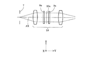
また、上述の実施形態では、第1補正フィルター8および第2補正フィルター9が入射位置に応じて透過率の異なる透過率分布を有するが、これに限定されることなく、入射角度に応じて透過率の異なる透過率分布を一対の補正フィルターに付与する変形例も可能である。この変形例では、たとえば図5に示すように、一方の補正フィルター8aが結像光学系10の瞳面10a(照明瞳面と光学的に共役な共役面)よりも光源側に配置され、他方の補正フィルター9aが結像光学系10の瞳面10aよりもマスク側に配置されることになる。
Further, in the above-described embodiment, the first correction filter 8 and the
この場合も、上述の実施形態および上述の変形例と同様の効果が得られる。すなわち、一対の補正フィルター8aおよび9aの透過率分布を相補的に設定し且つ結像光学系10の瞳面10aを挟んで一対の補正フィルター8aおよび9aを等距離に設定することにより、被照射面での照度分布をほぼ均一に維持しつつ、被照射面上の各点での瞳輝度分布をそれぞれほぼ均一に調整することができる。また、一対の補正フィルター8aおよび9aの透過率分布を実質的に相補的でない関係に設定するか、あるいは結像光学系10の瞳面10aを挟んで一対の補正フィルター8aおよび9aを互いに異なる距離に設定することにより、被照射面での照度分布をほぼ均一に調整しつつ、被照射面上の各点での瞳輝度分布をそれぞれほぼ均一に調整することができる。また、入射位置に応じて透過率の異なる透過率分布を有する補正フィルターと、入射角度に応じて透過率の異なる透過率分布を有する補正フィルターとを組み合わせて用いることや、入射位置に応じて透過率の異なる透過率分布を有する補正フィルター対(8,9)と、入射角度に応じて透過率の異なる透過率分布を有する補正フィルター対(8a,9a)とを組み合わせて用いることもできる。
Also in this case, the same effects as those of the above-described embodiment and the above-described modification can be obtained. That is, the transmittance distributions of the pair of
また、上述の説明では、一対の補正フィルター(8,9;8a,9a)に透過率分布を付与しているが、これに限定されることなく、入射位置に応じて反射率の異なる反射率分布を有する第1調整膜と第2調整膜とを用いることにより、あるいは入射角度に応じて反射率の異なる反射率分布を有する第1調整膜と第2調整膜とを用いることにより、上述の実施形態および上述の変形例と同様の効果が得られる。なお、入射位置または入射角度に応じて透過率分布を有する調整膜(補正フィルター)と、入射位置または入射角度に応じて反射率分布を有する調整膜とを組み合わせて用いてもよい。 In the above description, the transmittance distribution is given to the pair of correction filters (8, 9; 8a, 9a). However, the present invention is not limited to this, and the reflectance varies depending on the incident position. By using the first adjustment film and the second adjustment film having the distribution, or by using the first adjustment film and the second adjustment film having the reflectance distribution having different reflectances according to the incident angle, The same effects as those of the embodiment and the above-described modification can be obtained. Note that an adjustment film (correction filter) having a transmittance distribution according to the incident position or incident angle may be used in combination with an adjustment film having a reflectance distribution according to the incident position or incident angle.
また、上述の説明では、一対の補正フィルター(8,9;8a,9a)を用いることにより、換言すれば一対の調整膜を用いることにより、被照射面上の照度分布をほぼ均一に維持または調整しつつ被照射面上の各点での瞳輝度分布をそれぞれほぼ均一に調整している。しかしながら、これに限定されることなく、一般的には所定の透過率分布または反射率分布を有する複数の調整膜からなる調整手段を用いて、本発明の効果を得ることができる。すなわち、調整手段を構成する調整膜の数および配置について様々な変形例が可能である。 In the above description, by using a pair of correction filters (8, 9; 8a, 9a), in other words, by using a pair of adjustment films, the illuminance distribution on the irradiated surface is maintained substantially uniform or While adjusting, the pupil luminance distribution at each point on the irradiated surface is adjusted substantially uniformly. However, the present invention is not limited to this, and in general, the effect of the present invention can be obtained by using an adjusting means including a plurality of adjusting films having a predetermined transmittance distribution or reflectance distribution. That is, various modifications are possible with respect to the number and arrangement of adjustment films constituting the adjustment means.
具体的に、たとえば図6に示すように、入射位置に応じて透過率の異なる透過率分布を有する3つの補正フィルター11a〜11cを用いる変形例も可能である。図6の変形例では、マイクロフライアイレンズ5とマスクブラインド7との間のコンデンサー光学系6の光路中に第1補正フィルター11aおよび第2補正フィルター11bが光源側から順に配置され、コンデンサー光学系6とマスクブラインド7との間の光路中に第3補正フィルター11cが配置されている。
Specifically, for example, as shown in FIG. 6, a modification using three
この場合、図7に示すように、軸上光束(マスクブラインド7と光軸AXとの交点に達する光束)が補正フィルター11a〜11cをそれぞれ通過する領域すなわち軸上パーシャル領域11aa,11ba,11caが補正フィルター11a〜11c毎に異なっている。同様に、軸外光束(光軸AXから離れたマスクブラインド7上の点に達する光束)が補正フィルター11a〜11cをそれぞれ通過する領域すなわち軸外パーシャル領域11ab,11bb,11cbも補正フィルター11a〜11c毎に異なっている。
In this case, as shown in FIG. 7, areas where axial light beams (light beams reaching the intersection of the
この変形例では、各補正フィルター11a〜11cの透過率分布、各補正フィルター11a〜11cにおける軸上パーシャル領域および軸外パーシャル領域の位置および大きさなどを適宜設定することにより、被照射面での照度分布をほぼ均一に調整しつつ、被照射面上の各点での瞳輝度分布をそれぞれほぼ均一に調整することができる。さらに一般的には、入射位置または入射角度に応じて透過率(または反射率)が変化する所定の透過率分布(または反射率分布)を有する複数の調整膜からなる調整手段を用いて、各調整膜の透過率分布(または反射率分布)、各調整膜における軸上パーシャル領域および軸外パーシャル領域の位置および大きさなどを適宜設定することにより、本発明の効果を得ることができる。
In this modification, by appropriately setting the transmittance distribution of each
また、上述の説明では、平行平面板の形態を有する補正フィルターの光学平面上に所定の透過率分布(または反射率分布)を有する調整膜を形成しているが、これに限定されることなく、レンズや反射鏡の表面上に、すなわち凸状のレンズ面、凹状のレンズ面、凸状の反射面、凹状の反射面などの上に調整膜を形成することもできる。ただし、一般に、平面状の光学面を有する光学部材の光学平面上に調整膜を形成する方が製造容易であることはいうまでもない。 In the above description, the adjustment film having a predetermined transmittance distribution (or reflectance distribution) is formed on the optical plane of the correction filter having the form of a plane parallel plate. However, the present invention is not limited to this. The adjustment film may be formed on the surface of the lens or the reflecting mirror, that is, on the convex lens surface, the concave lens surface, the convex reflection surface, the concave reflection surface, or the like. However, it goes without saying that, in general, it is easier to produce an adjustment film on the optical plane of an optical member having a planar optical surface.
以下、光源1から投影光学系PLまでを被照射面としてのウェハWを照明する照明光学装置と考え、この照明光学装置(1〜PL)の調整方法について説明する。なお、本実施形態では、調整方法の説明を簡素化するために、所定の透過率分布を有する複数(2つまたはそれ以上)の補正フィルターを用いて、被照射面(ウェハWが設定される面)での照度分布をほぼ均一に調整しつつ、被照射面上の各点での瞳輝度分布をそれぞれほぼ均一に調整するものとする。
Hereinafter, the
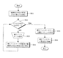
図8は、本実施形態にかかる照明光学装置の調整方法の各工程を概略的に示すフローチャートである。図8に示すように、本実施形態にかかる照明光学装置(1〜PL)の調整方法では、被照射面上の複数点に関する瞳輝度分布および被照射面における照度分布を得る(S11)。具体的に、分布獲得工程S11では、照明光学装置(1〜PL)の設計データに基づいて、被照射面上の複数点に関する瞳輝度分布および被照射面における照度分布を算出する。 FIG. 8 is a flowchart schematically showing each step of the adjustment method of the illumination optical apparatus according to the present embodiment. As shown in FIG. 8, in the adjustment method of the illumination optical apparatus (1 to PL) according to the present embodiment, the pupil luminance distribution regarding a plurality of points on the irradiated surface and the illuminance distribution on the irradiated surface are obtained (S11). Specifically, in the distribution acquisition step S11, based on the design data of the illumination optical device (1 to PL), the pupil luminance distribution regarding a plurality of points on the irradiated surface and the illuminance distribution on the irradiated surface are calculated.
ここで、照明光学装置(1〜PL)の設計データとして、たとえばマイクロフライアイレンズ5の直後からウェハWの直前までの光学系(6〜PL)のデータ、すなわち各光学面の曲率半径、各光学面の軸上間隔、各光学部材を形成する光学材料の屈折率および種類、使用光の波長、各光学部材の透過率、反射防止膜や反射膜の入射角度特性などのデータを用いる。なお、設計データに基づいて被照射面上の複数点に関する瞳輝度分布を算出する方法については、たとえば国際公開WO02/031570号パンフレットを参照することができる。また、設計データに基づいて被照射面における照度分布を算出する方法については良く知られおり、たとえば特開平3−216658号公報を参照することができる。 Here, as design data of the illumination optical device (1 to PL), for example, data of the optical system (6 to PL) from immediately after the micro fly's eye lens 5 to immediately before the wafer W, that is, the radius of curvature of each optical surface, Data such as the on-axis spacing of the optical surface, the refractive index and type of the optical material forming each optical member, the wavelength of the light used, the transmittance of each optical member, and the incident angle characteristics of the antireflection film and the reflection film are used. For a method of calculating pupil luminance distributions regarding a plurality of points on the irradiated surface based on design data, for example, International Publication WO02 / 031570 can be referred to. Further, a method for calculating the illuminance distribution on the irradiated surface based on the design data is well known. For example, Japanese Patent Laid-Open No. 3-216658 can be referred to.
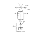
あるいは、分布獲得工程S11において、実際に製造された装置毎に被照射面上の複数点に関する瞳輝度分布および被照射面における照度分布を測定してもよい。具体的に、被照射面上の複数点に関する瞳輝度分布は、たとえば図9に示す分布計測装置20を用いて測定することができる。なお、分布計測装置20を用いる瞳輝度分布の測定は、ウェハWを光路から退避させた状態で行われる。分布計測装置20は、ピンホール部材20aと、集光レンズ20bと、たとえば二次元CCDのような光検出器20cとを有する。
Alternatively, in the distribution acquisition step S11, the pupil luminance distribution and the illuminance distribution on the irradiated surface for a plurality of points on the irradiated surface may be measured for each actually manufactured apparatus. Specifically, the pupil luminance distribution regarding a plurality of points on the irradiated surface can be measured using, for example, a
ここで、ピンホール部材20aは、投影光学系PLの結像面位置(すなわち露光に際してウェハWの被露光面が位置決めされるべき高さ位置)に配置されている。そして、ピンホール部材20aは集光レンズ20bの前側焦点位置に配置され、光検出器20cは集光レンズ20bの後側焦点位置に配置されている。したがって、光検出器20cの検出面は、投影光学系PLの開口絞りASの位置と光学的に共役な位置に配置されている。分布計測装置20では、投影光学系PLを通過した光が、ピンホール部材20aのピンホールを通過し、集光レンズ20bの集光作用を受けた後、光検出器20cの検出面に達する。
Here, the
こうして、光検出器20cの検出面には、開口絞りASの位置における光強度分布に対応する光強度分布が形成される。すなわち、分布計測装置20では、ピンホール部材20aのピンホールに達する光束が開口絞りASの位置(マイクロフライアイレンズ5の後側焦点面と光学的に共役な位置)に形成する光強度分布、すなわち被照射面上のピンホール点に関する瞳輝度分布が計測される。その結果、投影光学系PLの光軸AXと直交する面に沿ってウェハステージWSを二次元的に移動させてピンホール部材20aのピンホールの位置を二次元的に移動させつつ計測を繰り返すことにより、被照射面上の所望の複数点に関する瞳輝度分布を計測することができる。
Thus, a light intensity distribution corresponding to the light intensity distribution at the position of the aperture stop AS is formed on the detection surface of the
また、被照射面における照度分布は、たとえば図10に示す照度測定装置25を用いて測定することができる。照度測定装置25を用いる照度分布の測定も、ウェハWを光路から退避させた状態で行われる。照度測定装置25は、投影光学系PLの結像面(すなわち被照射面)における照度分布を計測するための光検出器として、たとえばフォトダイオード25aを備えている。フォトダイオード25aの出力は信号処理部25bに接続されている。
Further, the illuminance distribution on the irradiated surface can be measured using, for example, an
照度測定装置25では、投影光学系PLの光軸AXと直交する面に沿ったウェハステージWSの二次元的な移動により、フォトダイオード25aを介して投影光学系PLの結像面上の各位置における照度分布データを順次計測する。なお、複数のフォトダイオード25aを二次元的に配置し、ウェハステージWSを移動させることなく、投影光学系PLの結像面における照度分布データを一括的に計測する構成を採用することもできる。また、複数のフォトダイオード25aをライン状に配置し、ウェハステージWSを一次元的に移動させることにより、投影光学系PLの結像面における照度分布データを走査計測する構成を採用することもできる。
In the
次いで、本実施形態の調整方法では、設計データに基づく算出あるいは装置20および25を用いた測定により得られた被照射面上の複数点に関する瞳輝度分布および被照射面における照度分布がそれぞれ所望の程度にほぼ均一であるか否かを判定する(S12)。判定工程S12において、瞳輝度分布および照度分布のうちの少なくとも一方が所望の程度にほぼ均一でないと判定された場合(図中NOの場合)、補正フィルターの設計工程S13へ進む。一方、判定工程S12において、瞳輝度分布および照度分布の双方が所望の程度にほぼ均一であると判定された場合(図中YESの場合)、補正フィルターのドット濃密パターンの決定工程S15へ進む。
Next, in the adjustment method of the present embodiment, the pupil luminance distribution and the illuminance distribution on the irradiated surface for a plurality of points on the irradiated surface obtained by calculation based on the design data or measurement using the
設計工程S13では、瞳輝度分布および照度分布の双方が所望の程度にほぼ均一になるように、被照射面上の複数点に関する瞳輝度分布をそれぞれ独立的に調整し且つ必要に応じて被照射面における照度分布を調整するために複数の調整膜にそれぞれ付与すべき所要の透過率分布を決定(算出)する。具体的には、算出または測定された瞳輝度分布および照度分布の情報を参照して使用する補正フィルターの数および位置を予め想定し、被照射面での照度分布をほぼ均一に維持または調整しつつ被照射面上の各点での瞳輝度分布をそれぞれほぼ均一に調整するために各補正フィルターに付与すべき透過率分布を求める。 In the design step S13, the pupil luminance distributions related to a plurality of points on the irradiated surface are independently adjusted so that both the pupil luminance distribution and the illuminance distribution are substantially uniform to a desired level, and irradiated as necessary. In order to adjust the illuminance distribution on the surface, a required transmittance distribution to be provided to each of the plurality of adjustment films is determined (calculated). Specifically, the number and position of correction filters to be used are assumed in advance by referring to the calculated or measured pupil luminance distribution and illuminance distribution information, and the illuminance distribution on the irradiated surface is maintained or adjusted almost uniformly. On the other hand, in order to adjust the pupil luminance distribution at each point on the irradiated surface substantially uniformly, a transmittance distribution to be given to each correction filter is obtained.
次いで、設計工程S13で決定した透過率分布を付与した複数の補正フィルターをそれぞれ想定位置に配置した状態すなわち補正フィルターの搭載状態で、被照射面上の複数点に関する瞳輝度分布および被照射面における照度分布を算出する(S14)。具体的に、分布算出工程S14では、上述の設計データ情報に加えて各補正フィルターの透過率分布および位置に関する情報を参照して、瞳輝度分布および照度分布を算出する。 Next, in a state where the plurality of correction filters to which the transmittance distribution determined in the design step S13 is assigned are respectively arranged at the assumed positions, that is, in a state where the correction filter is mounted, the pupil luminance distribution on a plurality of points on the irradiated surface and the irradiated surface An illuminance distribution is calculated (S14). Specifically, in the distribution calculation step S14, the pupil luminance distribution and the illuminance distribution are calculated with reference to information on the transmittance distribution and position of each correction filter in addition to the above-described design data information.
次いで、分布算出工程S14で算出された被照射面上の複数点に関する瞳輝度分布および被照射面における照度分布がそれぞれ所望の程度にほぼ均一であるか否かを判定する(S12)。判定工程S12において、瞳輝度分布および照度分布のうちの少なくとも一方が所望の程度にほぼ均一でないと判定された場合(図中NOの場合)、再び補正フィルターの設計工程S13へ進むことになる。一方、判定工程S12において、瞳輝度分布および照度分布の双方が所望の程度にほぼ均一であると判定された場合(図中YESの場合)、補正フィルターのドット濃密パターンの決定工程S15へ進む。 Next, it is determined whether or not the pupil luminance distribution and the illuminance distribution on the irradiated surface calculated at the distribution calculating step S14 are substantially uniform to a desired degree (S12). If it is determined in the determination step S12 that at least one of the pupil luminance distribution and the illuminance distribution is not substantially uniform as desired (in the case of NO in the figure), the process proceeds to the correction filter design step S13 again. On the other hand, in the determination step S12, when it is determined that both the pupil luminance distribution and the illuminance distribution are substantially uniform to a desired degree (in the case of YES in the figure), the process proceeds to the determination step S15 for the dot dense pattern of the correction filter.
たとえば試行錯誤的に設計工程S13と分布算出工程S14とを繰り返して進んだパターン決定工程S15では、設計工程S13で算出された所要の透過率分布(各補正フィルターに付与すべき透過率分布)を実現するのに必要な遮光性ドットの濃密パターンを決定する。最後に、パターン決定工程S15で決定されたドット濃密パターンを有する複数の補正フィルターを製造し、製造された各補正フィルターを光学系中の所定の位置にそれぞれ組み込む(S16)。以上のように、パターン決定工程S15および製造搭載工程S16は、所要の透過率分布を有する複数の調整膜をそれぞれ形成して配置する調整工程を構成している。こうして、本実施形態の調整方法は終了する。 For example, in the pattern determination step S15 that has advanced by repeating the design step S13 and the distribution calculation step S14 on a trial and error basis, the required transmittance distribution calculated in the design step S13 (the transmittance distribution to be given to each correction filter) is obtained. A dense pattern of light-shielding dots necessary for realization is determined. Finally, a plurality of correction filters having the dense dot pattern determined in the pattern determination step S15 are manufactured, and each of the manufactured correction filters is incorporated at a predetermined position in the optical system (S16). As described above, the pattern determination step S15 and the manufacturing and mounting step S16 constitute an adjustment step in which a plurality of adjustment films each having a required transmittance distribution are formed and arranged. Thus, the adjustment method of this embodiment is completed.
次に、本実施形態の変形例として、各補正フィルターに付与すべき所要の透過率分布を試行錯誤的ではなく簡易に且つ正確に求めることのできる調整方法を説明する。図11は、本実施形態の変形例にかかる調整方法の各工程を概略的に示すフローチャートである。図11に示す変形例の調整方法では、図8に示す調整方法と同様に、被照射面上の複数点に関する瞳輝度分布および被照射面における照度分布を得る(S21)。具体的に、分布獲得工程S21では、照明光学装置(1〜PL)の設計データに基づいて、被照射面上の複数点に関する瞳輝度分布および被照射面における照度分布を算出する。あるいは、上述の装置20および25を用いて、実際に製造された装置毎に被照射面上の複数点に関する瞳輝度分布および被照射面における照度分布を測定する。
Next, as a modification of the present embodiment, an adjustment method that can easily and accurately obtain a required transmittance distribution to be given to each correction filter, rather than trial and error, will be described. FIG. 11 is a flowchart schematically showing each step of the adjustment method according to the modification of the present embodiment. In the adjustment method of the modification shown in FIG. 11, the pupil luminance distribution and the illuminance distribution on the irradiated surface are obtained for a plurality of points on the irradiated surface, similarly to the adjusting method shown in FIG. 8 (S21). Specifically, in the distribution acquisition step S <b> 21, based on the design data of the illumination optical device (1 -PL), the pupil luminance distribution regarding a plurality of points on the irradiated surface and the illuminance distribution on the irradiated surface are calculated. Alternatively, the above-described
次いで、図8に示す調整方法と同様に、設計データに基づく算出あるいは装置20および25を用いた測定により得られた被照射面上の複数点に関する瞳輝度分布および被照射面における照度分布がそれぞれ所望の程度にほぼ均一であるか否かを判定する(S22)。判定工程S22において、瞳輝度分布および照度分布のうちの少なくとも一方が所望の程度にほぼ均一でないと判定された場合(図中NOの場合)、瞳輝度分布の近似工程S23へ進む。一方、判定工程S22において、瞳輝度分布および照度分布の双方が所望の程度にほぼ均一であると判定された場合(図中YESの場合)、補正フィルターのドット濃密パターンの決定工程S27へ進む。
Next, similarly to the adjustment method shown in FIG. 8, the pupil luminance distribution and the illuminance distribution on the irradiated surface obtained by calculation based on design data or measurement using the
瞳輝度分布の近似工程S23では、分布獲得工程S21で得られた被照射面上の各点に関する瞳輝度分布を照明瞳面における瞳座標の関数としての所定の多項式で近似する。具体的には、たとえば座標系として照明瞳面における瞳極座標(ρ,θ)を用いるツェルニケの円筒関数Zi(ρ,θ)を含むツェルニケ多項式で、投影光学系PLの像面(被照射面)上の各点に関する瞳輝度分布をそれぞれフィッティング(近似)する。ここで、投影光学系PLの像面座標と瞳座標との関係、すなわち像面直交座標(y,z)と瞳直交座標(ξ,η)と像面極座標(h,α)と瞳極座標(ρ,θ)との関係は、図12に概略的に示す通りである。ここで、hおよびρは規格化半怪であり、αおよびθは極座標の動径角である。 In the pupil luminance distribution approximation step S23, the pupil luminance distribution relating to each point on the irradiated surface obtained in the distribution acquisition step S21 is approximated by a predetermined polynomial as a function of pupil coordinates on the illumination pupil plane. Specifically, for example, a Zernike polynomial including a Zernike cylindrical function Zi (ρ, θ) using pupil polar coordinates (ρ, θ) on the illumination pupil plane as a coordinate system, and an image plane (irradiated surface) of the projection optical system PL. Fitting (approximate) the pupil luminance distribution for each point above. Here, the relationship between the image plane coordinates and pupil coordinates of the projection optical system PL, that is, image plane orthogonal coordinates (y, z), pupil orthogonal coordinates (ξ, η), image plane polar coordinates (h, α), and pupil polar coordinates ( The relationship with [rho], [theta] is as schematically shown in FIG. Here, h and ρ are standardized half mysteries, and α and θ are radial angles of polar coordinates.
瞳輝度分布I(ρ,θ)は、投影光学系PLの像面上の各点について、ツェルニケの円筒関数Zi(ρ,θ)を用いて、次の式(1)に示すように展開される。
I(ρ,θ)=ΣCi・Zi(ρ,θ)
=C1・Z1(ρ,θ)+C2・Z2(ρ,θ)
・・・+Cn・Zn(ρ,θ) (1)
The pupil luminance distribution I (ρ, θ) is developed as shown in the following equation (1) using the Zernike cylindrical function Zi (ρ, θ) for each point on the image plane of the projection optical system PL. The
I (ρ, θ) = ΣCi · Zi (ρ, θ)
= C1 · Z1 (ρ, θ) + C2 · Z2 (ρ, θ)
... + Cn · Zn (ρ, θ) (1)
ここで、Ciは、ツェルニケ多項式の各項の係数である。以下、ツェルニケ多項式の各項の関数系Zi(ρ,θ)のうち、第1項〜第36項にかかる関数Z1〜Z36を、次の表(1)に示す。 Here, Ci is a coefficient of each term of the Zernike polynomial. Hereinafter, among the function system Zi (ρ, θ) of each term of the Zernike polynomial, functions Z1 to Z36 relating to the first term to the 36th term are shown in the following table (1).
表(1)
Z1: 1
Z2: ρcosθ
Z3: ρsinθ
Z4: 2ρ2−1
Z5: ρ2cos2θ
Z6: ρ2sin2θ
Z7: (3ρ2−2)ρcosθ
Z8: (3ρ2−2)ρsinθ
Z9: 6ρ4−6ρ2+1
Z10: ρ3cos3θ
Z11: ρ3sin3θ
Z12: (4ρ2−3)ρ2cos2θ
Z13: (4ρ2−3)ρ2sin2θ
Z14: (10ρ4−12ρ2+3)ρcosθ
Z15: (10ρ4−12ρ2+3)ρsinθ
Z16: 20ρ6−30ρ4+12ρ2−1
Z17: ρ4cos4θ
Z18: ρ4sin4θ
Z19: (5ρ2−4)ρ3cos3θ
Z20: (5ρ2−4)ρ3sin3θ
Z21: (15ρ4−20ρ2+6)ρ2cos2θ
Z22: (15ρ4−20ρ2+6)ρ2sin2θ
Z23: (35ρ6−60ρ4+30ρ2−4)ρcosθ
Z24: (35ρ6−60ρ4+30ρ2−4)ρsinθ
Z25: 70ρ8−140ρ6+90ρ4−20ρ2+1
Z26: ρ5cos5θ
Z27: ρ5sin5θ
Z28: (6ρ2−5)ρ4cos4θ
Z29: (6ρ2−5)ρ4sin4θ
Z30: (21ρ4−30ρ2+10)ρ3cos3θ
Z31: (21ρ4−30ρ2+10)ρ3sin3θ
Z32: (56ρ6−104ρ4+60ρ2−10)ρ2cos2θ
Z33: (56ρ6−104ρ4+60ρ2−10)ρ2sin2θ
Z34: (126ρ8−280ρ6+210ρ4−60ρ2+5)ρcosθ
Z35: (126ρ8−280ρ6+210ρ4−60ρ2+5)ρsinθ
Z36: 252ρ10−630ρ8+560ρ6−210ρ4+30ρ2−1
Table (1)
Z1: 1
Z2: ρcosθ
Z3: ρsinθ
Z4: 2ρ 2 −1
Z5: ρ 2 cos2θ
Z6: ρ 2 sin2θ
Z7: (3ρ 2 -2) ρcosθ
Z8: (3ρ 2 -2) ρsinθ
Z9: 6ρ 4 -6ρ 2 +1
Z10: ρ 3 cos3θ
Z11: ρ 3 sin3θ
Z12: (4ρ 2 -3) ρ 2 cos2θ
Z13: (4ρ 2 -3) ρ 2 sin2θ
Z14: (10ρ 4 −12ρ 2 +3) ρcosθ
Z15: (10ρ 4 −12ρ 2 +3) ρsinθ
Z16: 20ρ 6 −30ρ 4 + 12ρ 2 −1
Z17: ρ 4 cos4θ
Z18: ρ 4 sin4θ
Z19: (5ρ 2 -4) ρ 3 cos3θ
Z20: (5ρ 2 -4) ρ 3 sin3θ
Z21: (15ρ 4 −20ρ 2 +6) ρ 2 cos 2θ
Z22: (15ρ 4 −20ρ 2 +6) ρ 2 sin2θ
Z23: (35ρ 6 -60ρ 4 + 30ρ 2 -4) ρcosθ
Z24: (35ρ 6 -60ρ 4 + 30ρ 2 -4) ρsinθ
Z25: 70ρ 8 −140ρ 6 + 90ρ 4 −20ρ 2 +1
Z26: ρ 5 cos 5θ
Z27: ρ 5 sin5θ
Z28: (6ρ 2 -5) ρ 4 cos4θ
Z29: (6ρ 2 -5) ρ 4 sin4θ
Z30: (21ρ 4 −30ρ 2 +10) ρ 3 cos3θ
Z31: (21ρ 4 −30ρ 2 +10) ρ 3 sin3θ
Z32: (56ρ 6 −104ρ 4 + 60ρ 2 −10) ρ 2 cos 2θ
Z33: (56ρ 6 −104ρ 4 + 60ρ 2 −10) ρ 2 sin2θ
Z34: (126ρ 8 -280ρ 6 + 210ρ 4 -60ρ 2 +5) ρcosθ
Z35: (126ρ 8 −280ρ 6 + 210ρ 4 −60ρ 2 +5) ρsinθ
Z36: 252ρ 10 −630ρ 8 + 560ρ 6 −210ρ 4 + 30ρ 2 −1
したがって、近似工程S23では、被照射面(投影光学系PLの像面)上の複数点について得られた瞳輝度分布をツェルニケ多項式でフィッティングし、各項のツェルニケ係数Ciを各点について算出する。なお、瞳輝度分布(瞳透過率分布)のツェルニケ多項式によるフィッティング手法については、前述の国際公開WO02/031570号パンフレットや特開2004−126010号公報を参照することができる。 Therefore, in the approximation step S23, the pupil luminance distribution obtained for a plurality of points on the irradiated surface (image surface of the projection optical system PL) is fitted with a Zernike polynomial, and the Zernike coefficient Ci of each term is calculated for each point. For the fitting method using the Zernike polynomial for the pupil luminance distribution (pupil transmittance distribution), the above-mentioned International Publication WO 02/031570 pamphlet and Japanese Patent Application Laid-Open No. 2004-126010 can be referred to.
次いで、本変形例の調整方法では、近似工程S23で得られたツェルニケ多項式における各項の係数Ciに基づいて、各点に関する瞳輝度分布を像面極座標(h,α)および瞳極座標(ρ,θ)の関数としての瞳輝度分布多項式により評価する(S24)。具体的に、評価工程S24では、各点に関する瞳輝度分布を像面極座標(h,α)および瞳極座標(ρ,θ)の関数として表す瞳輝度分布多項式を設定する。なお、瞳輝度分布多項式の設定については、特開2003−257812号公報や特願2004−149698号明細書および図面を参照することができる。 Next, in the adjustment method of this modification, based on the coefficient Ci of each term in the Zernike polynomial obtained in the approximation step S23, the pupil luminance distribution for each point is converted into the image plane polar coordinates (h, α) and the pupil polar coordinates (ρ, Evaluation is performed by a pupil luminance distribution polynomial as a function of θ) (S24). Specifically, in the evaluation step S24, a pupil luminance distribution polynomial is set that represents the pupil luminance distribution for each point as a function of image plane polar coordinates (h, α) and pupil polar coordinates (ρ, θ). Regarding the setting of the pupil luminance distribution polynomial, Japanese Patent Application Laid-Open No. 2003-257812 and Japanese Patent Application No. 2004-149698 and drawings can be referred to.
上述の公報などでは、投影光学系の波面収差を像面極座標(h,α)および瞳極座標(ρ,θ)の関数として表す収差多項式を設定しているが、同様の手法により瞳輝度分布多項式を設定することができることは明らかである。こうして、評価工程S24では、近似工程(S23)で得られたツェルニケ多項式における各項のツェルニケ係数Ciに基づいて、瞳輝度分布多項式における各項の係数を決定し、ひいては各点に関する瞳輝度分布を瞳輝度分布多項式により表して評価する。 In the above-mentioned publications and the like, an aberration polynomial that sets the wavefront aberration of the projection optical system as a function of image plane polar coordinates (h, α) and pupil polar coordinates (ρ, θ) is set. It is clear that can be set. Thus, in the evaluation step S24, the coefficient of each term in the pupil luminance distribution polynomial is determined based on the Zernike coefficient Ci of each term in the Zernike polynomial obtained in the approximation step (S23), and consequently the pupil luminance distribution for each point is determined. The evaluation is expressed by a pupil luminance distribution polynomial.
具体的には、上述の公報などに開示されているように、たとえば特定項のツェルニケ関数Ziに着目し、対応するツェルニケ係数Ciの像面内分布(各点における係数Ciの分布)に基づいて、瞳輝度分布多項式における特定項の係数を例えば最小二乗法を用いて決定する。さらに、他の特定項のツェルニケ関数Ziに着目し、対応するツェルニケ係数Ciの像面内分布に基づいて、瞳輝度分布多項式における他の項の係数を例えば最小二乗法を用いて順次決定する。 Specifically, as disclosed in the above-mentioned publications, for example, focusing on the Zernike function Zi of a specific term, based on the in-image distribution of the corresponding Zernike coefficient Ci (distribution of the coefficient Ci at each point) The coefficient of the specific term in the pupil luminance distribution polynomial is determined using, for example, the least square method. Further, paying attention to the Zernike function Zi of another specific term, the coefficient of the other term in the pupil luminance distribution polynomial is sequentially determined using, for example, the least square method based on the in-image distribution of the corresponding Zernike coefficient Ci.
こうして、評価工程S24では、瞳輝度分布の瞳内分布および像面内分布を同時に表現する瞳輝度分布多項式が最終的に得られる。このように、瞳輝度分布の瞳内分布および像面内分布を同時に表現する瞳輝度分布多項式を用いることにより、瞳輝度分布を解析的に分解することが可能になり、コンピュータを使って試行錯誤的に数値最適化を行う手法に比して、光学調整解を迅速に且つ正確に算出することが可能になる。つまり、瞳輝度分布多項式により瞳輝度分布状況の特徴を把握し易くなるので、光学調整の見通しが立て易くなる。 Thus, in the evaluation step S24, a pupil luminance distribution polynomial that simultaneously represents the in-pupil distribution and the in-plane distribution of the pupil luminance distribution is finally obtained. In this way, the pupil luminance distribution polynomial can be analyzed analytically by using the pupil luminance distribution polynomial that simultaneously expresses the pupil luminance distribution in the pupil and the in-plane distribution, and trial and error can be performed using a computer. Therefore, it is possible to calculate the optical adjustment solution quickly and accurately as compared with the method of performing numerical optimization. That is, since it becomes easy to grasp the characteristics of the pupil luminance distribution situation by the pupil luminance distribution polynomial, it is easy to make a prospect of optical adjustment.
次いで、補正フィルターの設計工程S25では、瞳輝度分布および照度分布の双方が所望の程度にほぼ均一になるように、被照射面上の複数点に関する瞳輝度分布をそれぞれ独立的に調整し且つ必要に応じて被照射面における照度分布を調整するために複数の調整膜にそれぞれ付与すべき所要の透過率分布を決定(算出)する。具体的には、まず必要に応じて、分布獲得工程S21で得られた被照射面における照度分布を像面極座標(h,α)の関数としてのツェルニケ多項式により近似しておく。 Next, in the correction filter design step S25, the pupil luminance distributions related to a plurality of points on the irradiated surface are independently adjusted and necessary so that both the pupil luminance distribution and the illuminance distribution are substantially uniform to a desired level. In order to adjust the illuminance distribution on the surface to be irradiated, a required transmittance distribution to be applied to each of the plurality of adjustment films is determined (calculated). Specifically, first, if necessary, the illuminance distribution on the irradiated surface obtained in the distribution acquisition step S21 is approximated by a Zernike polynomial as a function of image plane polar coordinates (h, α).
また、各補正フィルターに付与すべき透過率分布を、たとえば調整膜としての光学面における極座標を用いたツェルニケ多項式により表現する。そして、各補正フィルターの透過率分布を表すツェルニケ多項式の各項の係数と被照射面上の各点に関する瞳輝度分布の変化との関係を表す第1テーブルT21、および各補正フィルターの透過率分布を表すツェルニケ多項式の各項の係数と被照射面における照度分布の変化との関係を表す第2テーブルT22を準備する。 Further, the transmittance distribution to be given to each correction filter is expressed by, for example, a Zernike polynomial using polar coordinates on the optical surface as an adjustment film. The first table T21 representing the relationship between the coefficient of each term of the Zernike polynomial representing the transmittance distribution of each correction filter and the change in pupil luminance distribution for each point on the irradiated surface, and the transmittance distribution of each correction filter A second table T22 representing the relationship between the coefficient of each term of the Zernike polynomial representing the change in the illuminance distribution on the irradiated surface is prepared.
こうして、設計工程S25では、評価工程S24で得られた瞳輝度分布に関する評価結果(具体的には瞳輝度分布の瞳内分布および像面内分布を同時に表現する瞳輝度分布多項式)、必要に応じてツェルニケ多項式により近似された照度分布情報、第1テーブルT21における各補正フィルターの透過率分布と瞳輝度分布の変化との相関関係、および第2テーブルT22における各補正フィルターの透過率分布と照度分布の変化との相関関係を参照した線形結合による最適化手法に基づいて、被照射面での照度分布をほぼ均一に維持または調整しつつ被照射面上の各点での瞳輝度分布をそれぞれほぼ均一に調整するために各補正フィルターに付与すべき透過率分布を求める。 In this way, in the design step S25, the evaluation result regarding the pupil luminance distribution obtained in the evaluation step S24 (specifically, the pupil luminance distribution polynomial that simultaneously expresses the in-pupil distribution and the in-plane distribution of the pupil luminance distribution), if necessary Illuminance distribution information approximated by a Zernike polynomial, correlation between transmittance distribution of each correction filter and pupil luminance distribution in the first table T21, and transmittance distribution and illuminance distribution of each correction filter in the second table T22 Based on an optimization method based on a linear combination that refers to the correlation with the change in the illumination, the luminance distribution on the irradiated surface is maintained or adjusted almost uniformly, and the pupil luminance distribution at each point on the irradiated surface is approximately In order to make uniform adjustment, a transmittance distribution to be given to each correction filter is obtained.
次いで、設計工程S25で決定した透過率分布を付与した複数の補正フィルターをそれぞれ想定位置に配置した状態すなわち補正フィルターの搭載状態で、被照射面上の複数点に関する瞳輝度分布および被照射面における照度分布を算出する(S26)。さらに、分布算出工程S26で算出された被照射面上の複数点に関する瞳輝度分布および被照射面における照度分布がそれぞれ所望の程度にほぼ均一であるか否かを判定する(S22)。線形結合による最適化手法を用いて所要の透過率分布が試行錯誤的ではなく簡易に且つ正確に求められているので、判定工程S22において瞳輝度分布および照度分布の双方が所望の程度にほぼ均一であると判定され、補正フィルターのドット濃密パターンの決定工程S27へ進むことになる。 Next, in a state where the plurality of correction filters to which the transmittance distribution determined in the design step S25 is assigned are respectively arranged at the assumed positions, that is, in a state where the correction filter is mounted, the pupil luminance distributions on a plurality of points on the irradiated surface and the irradiated surface An illuminance distribution is calculated (S26). Further, it is determined whether or not the pupil luminance distribution and the illuminance distribution on the irradiated surface calculated at the distribution calculating step S26 are substantially uniform to a desired degree (S22). Since the required transmittance distribution is obtained easily and accurately using an optimization method based on linear combination, not both trial and error, both the pupil luminance distribution and the illuminance distribution are substantially uniform to a desired level in the determination step S22. Therefore, the process proceeds to a correction filter dot dense pattern determination step S27.
パターン決定工程S27では、設計工程S25で算出された所要の透過率分布(各補正フィルターに付与すべき透過率分布)を実現するのに必要な遮光性ドットの濃密パターンを決定する。最後に、パターン決定工程S27で決定されたドット濃密パターンを有する複数の補正フィルターを製造し、製造された各補正フィルターを光学系中の所定の位置にそれぞれ組み込む(S28)。こうして、変形例の調整方法は終了する。 In the pattern determination step S27, a dense pattern of light-shielding dots necessary to realize the required transmittance distribution (transmittance distribution to be given to each correction filter) calculated in the design step S25 is determined. Finally, a plurality of correction filters having the dense dot pattern determined in the pattern determination step S27 are manufactured, and each manufactured correction filter is incorporated into a predetermined position in the optical system (S28). In this way, the adjustment method of a modification is complete | finished.
上述の実施形態にかかる露光装置では、照明光学装置によってマスク(レチクル)を照明し(照明工程)、投影光学系を用いてマスクに形成された転写用のパターンを感光性基板に露光する(露光工程)ことにより、マイクロデバイス(半導体素子、撮像素子、液晶表示素子、薄膜磁気ヘッド等)を製造することができる。以下、上述の実施形態の露光装置を用いて感光性基板としてのウェハ等に所定の回路パターンを形成することによって、マイクロデバイスとしての半導体デバイスを得る際の手法の一例につき図13のフローチャートを参照して説明する。 In the exposure apparatus according to the above-described embodiment, the illumination optical device illuminates the mask (reticle) (illumination process), and the projection optical system is used to expose the transfer pattern formed on the mask onto the photosensitive substrate (exposure). Step), a micro device (semiconductor element, imaging element, liquid crystal display element, thin film magnetic head, etc.) can be manufactured. Hereinafter, refer to the flowchart of FIG. 13 for an example of a method for obtaining a semiconductor device as a micro device by forming a predetermined circuit pattern on a wafer or the like as a photosensitive substrate using the exposure apparatus of the above-described embodiment. To explain.
先ず、図13のステップ301において、1ロットのウェハ上に金属膜が蒸着される。次のステップ302において、その1ロットのウェハ上の金属膜上にフォトレジストが塗布される。その後、ステップ303において、上述の実施形態の露光装置を用いて、マスク上のパターンの像がその投影光学系を介して、その1ロットのウェハ上の各ショット領域に順次露光転写される。その後、ステップ304において、その1ロットのウェハ上のフォトレジストの現像が行われた後、ステップ305において、その1ロットのウェハ上でレジストパターンをマスクとしてエッチングを行うことによって、マスク上のパターンに対応する回路パターンが、各ウェハ上の各ショット領域に形成される。その後、更に上のレイヤの回路パターンの形成等を行うことによって、半導体素子等のデバイスが製造される。上述の半導体デバイス製造方法によれば、極めて微細な回路パターンを有する半導体デバイスをスループット良く得ることができる。 First, in step 301 of FIG. 13, a metal film is deposited on one lot of wafers. In the next step 302, a photoresist is applied on the metal film on the one lot of wafers. Thereafter, in step 303, the image of the pattern on the mask is sequentially exposed and transferred to each shot area on the wafer of one lot through the projection optical system using the exposure apparatus of the above-described embodiment. Thereafter, in step 304, the photoresist on the one lot of wafers is developed, and in step 305, the resist pattern is etched on the one lot of wafers to form a pattern on the mask. Corresponding circuit patterns are formed in each shot area on each wafer. Thereafter, a device pattern such as a semiconductor element is manufactured by forming a circuit pattern of an upper layer. According to the semiconductor device manufacturing method described above, a semiconductor device having an extremely fine circuit pattern can be obtained with high throughput.
また、上述の実施形態の露光装置では、プレート(ガラス基板)上に所定のパターン(回路パターン、電極パターン等)を形成することによって、マイクロデバイスとしての液晶表示素子を得ることもできる。以下、図14のフローチャートを参照して、このときの手法の一例につき説明する。図14において、パターン形成工程401では、上述の実施形態の露光装置を用いてマスクのパターンを感光性基板(レジストが塗布されたガラス基板等)に転写露光する、所謂光リソグラフィー工程が実行される。この光リソグラフィー工程によって、感光性基板上には多数の電極等を含む所定パターンが形成される。その後、露光された基板は、現像工程、エッチング工程、レジスト剥離工程等の各工程を経ることによって、基板上に所定のパターンが形成され、次のカラーフィルター形成工程402へ移行する。 In the exposure apparatus of the above-described embodiment, a liquid crystal display element as a micro device can be obtained by forming a predetermined pattern (circuit pattern, electrode pattern, etc.) on a plate (glass substrate). Hereinafter, an example of the technique at this time will be described with reference to the flowchart of FIG. In FIG. 14, in the pattern formation process 401, a so-called photolithography process is performed in which the exposure pattern of the above-described embodiment is used to transfer and expose a mask pattern onto a photosensitive substrate (such as a glass substrate coated with a resist). . By this photolithography process, a predetermined pattern including a large number of electrodes and the like is formed on the photosensitive substrate. Thereafter, the exposed substrate undergoes steps such as a developing step, an etching step, and a resist stripping step, whereby a predetermined pattern is formed on the substrate, and the process proceeds to the next color filter forming step 402.
次に、カラーフィルター形成工程402では、R(Red)、G(Green)、B(Blue)に対応した3つのドットの組がマトリックス状に多数配列されたり、またはR、G、Bの3本のストライプのフィルターの組を複数水平走査線方向に配列したカラーフィルターを形成する。そして、カラーフィルター形成工程402の後に、セル組み立て工程403が実行される。セル組み立て工程403では、パターン形成工程401にて得られた所定パターンを有する基板、およびカラーフィルター形成工程402にて得られたカラーフィルター等を用いて液晶パネル(液晶セル)を組み立てる。 Next, in the color filter forming step 402, a large number of sets of three dots corresponding to R (Red), G (Green), and B (Blue) are arranged in a matrix or three of R, G, and B A color filter is formed by arranging a plurality of stripe filter sets in the horizontal scanning line direction. Then, after the color filter forming step 402, a cell assembly step 403 is executed. In the cell assembly step 403, a liquid crystal panel (liquid crystal cell) is assembled using the substrate having the predetermined pattern obtained in the pattern formation step 401, the color filter obtained in the color filter formation step 402, and the like.
セル組み立て工程403では、例えば、パターン形成工程401にて得られた所定パターンを有する基板とカラーフィルター形成工程402にて得られたカラーフィルターとの間に液晶を注入して、液晶パネル(液晶セル)を製造する。その後、モジュール組み立て工程404にて、組み立てられた液晶パネル(液晶セル)の表示動作を行わせる電気回路、バックライト等の各部品を取り付けて液晶表示素子として完成させる。上述の液晶表示素子の製造方法によれば、極めて微細な回路パターンを有する液晶表示素子をスループット良く得ることができる。 In the cell assembly step 403, for example, liquid crystal is injected between the substrate having the predetermined pattern obtained in the pattern formation step 401 and the color filter obtained in the color filter formation step 402, and a liquid crystal panel (liquid crystal cell) is obtained. ). Thereafter, in a module assembling step 404, components such as an electric circuit and a backlight for performing a display operation of the assembled liquid crystal panel (liquid crystal cell) are attached to complete a liquid crystal display element. According to the above-described method for manufacturing a liquid crystal display element, a liquid crystal display element having an extremely fine circuit pattern can be obtained with high throughput.
なお、上述の実施形態では、露光光としてKrFエキシマレーザ光(波長:248nm)やArFエキシマレーザ光(波長:193nm)を用いているが、これに限定されることなく、他の適当なレーザ光源、たとえば波長157nmのレーザ光を供給するF2レーザ光源などに対して本発明を適用することもできる。さらに、上述の実施形態では、照明光学装置を備えた露光装置を例にとって本発明を説明したが、マスクやウェハ以外の被照射面を照明するための一般的な照明光学装置に本発明を適用することができることは明らかである。 In the above-described embodiment, KrF excimer laser light (wavelength: 248 nm) or ArF excimer laser light (wavelength: 193 nm) is used as the exposure light. However, the present invention is not limited to this, and other suitable laser light sources. For example, the present invention can also be applied to an F 2 laser light source that supplies laser light having a wavelength of 157 nm. Furthermore, in the above-described embodiment, the present invention has been described by taking an exposure apparatus provided with an illumination optical apparatus as an example. Obviously you can do that.
また、上述の実施形態において、投影光学系と感光性基板との間の光路中を1.1よりも大きな屈折率を有する媒体(典型的には液体)で満たす手法、所謂液浸法を適用しても良い。この場合、投影光学系と感光性基板との間の光路中に液体を満たす手法としては、国際公開番号WO99/49504号公報に開示されているような局所的に液体を満たす手法や、特開平6−124873号公報に開示されているような露光対象の基板を保持したステージを液槽の中で移動させる手法や、特開平10−303114号公報に開示されているようなステージ上に所定深さの液体槽を形成し、その中に基板を保持する手法などを採用することができる。 In the above-described embodiment, a so-called immersion method is applied in which the optical path between the projection optical system and the photosensitive substrate is filled with a medium (typically liquid) having a refractive index larger than 1.1. You may do it. In this case, as a method of filling the liquid in the optical path between the projection optical system and the photosensitive substrate, a method of locally filling the liquid as disclosed in International Publication No. WO99 / 49504, A method of moving a stage holding a substrate to be exposed as disclosed in Japanese Patent Application Laid-Open No. 6-124873 in a liquid bath, or a predetermined depth on a stage as disclosed in Japanese Patent Application Laid-Open No. 10-303114. A technique of forming a liquid tank and holding the substrate in the liquid tank can be employed.
なお、液体としては、露光光に対する透過性があってできるだけ屈折率が高く、投影光学系や基板表面に塗布されているフォトレジストに対して安定なものを用いることが好ましく、たとえばKrFエキシマレーザ光やArFエキシマレーザ光を露光光とする場合には、液体として純水、脱イオン水を用いることができる。また、露光光としてF2レーザ光を用いる場合は、液体としてはF2レーザ光を透過可能な例えばフッ素系オイルや過フッ化ポリエーテル(PFPE)等のフッ素系の液体を用いればよい。 As the liquid, it is preferable to use a liquid that is transmissive to exposure light and has a refractive index as high as possible, and is stable with respect to a photoresist applied to the projection optical system and the substrate surface, for example, KrF excimer laser light. When ArF excimer laser light is used as exposure light, pure water or deionized water can be used as the liquid. When F 2 laser light is used as exposure light, a fluorine-based liquid such as fluorine oil or perfluorinated polyether (PFPE) that can transmit the F 2 laser light may be used as the liquid.
1 光源
3 回折光学素子
4 ズームレンズ
5 マイクロフライアイレンズ(フライアイレンズ)
6 コンデンサー光学系
7 マスクブラインド
8,8a,9,9a 補正フィルター
10 結像光学系
20 分布計測装置
25 照度測定装置
M マスク
MS マスクステージ
PL 投影光学系
W ウェハ
WS ウェハステージ
DESCRIPTION OF
6 Condenser
Claims (30)
前記被照射面上における第1の点に達する第1光束に関する瞳輝度分布を得る第1瞳輝度分布獲得工程と、
前記被照射面上における前記第1の点とは異なる第2の点に達する第2光束に関する瞳輝度分布を得る第2瞳輝度分布獲得工程と、
前記第1および第2の点に関する瞳輝度分布をそれぞれ独立に調整するために、前記照明光学装置の光路中の複数の位置での所要の透過率分布または反射率分布を決定する分布決定工程と、
前記所要の透過率分布または反射率分布を有する複数の調整膜をそれぞれ形成して前記複数の位置に配置する調整工程とを含むことを特徴とする調整方法。 In a method for adjusting an illumination optical device that forms a pupil luminance distribution having a predetermined luminance distribution on an illumination pupil plane based on a luminous flux from a light source, and illuminates an illuminated surface with the luminous flux from the pupil luminance distribution,
A first pupil luminance distribution obtaining step for obtaining a pupil luminance distribution relating to a first light flux reaching the first point on the irradiated surface;
A second pupil luminance distribution obtaining step for obtaining a pupil luminance distribution related to a second light flux reaching a second point different from the first point on the irradiated surface;
A distribution determining step of determining required transmittance distributions or reflectance distributions at a plurality of positions in the optical path of the illumination optical device in order to independently adjust pupil luminance distributions related to the first and second points; ,
And an adjusting step of forming a plurality of adjusting films having the required transmittance distribution or reflectance distribution and arranging the adjusting films at the plurality of positions, respectively.
前記分布決定工程では、前記照度分布を調整するために、前記照明光学装置の光路中の前記第1及び第2の位置での所要の透過率分布または反射率分布を算出することを特徴とする請求項1に記載の調整方法。 An illuminance distribution obtaining step of obtaining an illuminance distribution on the irradiated surface;
In the distribution determination step, in order to adjust the illuminance distribution, a required transmittance distribution or reflectance distribution at the first and second positions in the optical path of the illumination optical device is calculated. The adjustment method according to claim 1.
前記被照射面上における第1の点に達する第1光束に関する瞳輝度分布を得る第1瞳輝度分布獲得工程と、
前記被照射面上における前記第1の点とは異なる第2の点に達する第2光束に関する瞳輝度分布を得る第2瞳輝度分布獲得工程と、
前記第1および第2の点に関する瞳輝度分布をそれぞれ独立に調整するために、前記照明光学装置の光路中の複数の位置での所要の透過率分布または反射率分布を決定する分布決定工程と、
前記所要の透過率分布または反射率分布を有する複数の調整膜をそれぞれ形成して前記複数の位置に配置する調整工程とを含み、
前記調整工程では、前記複数の調整膜の間の距離を決定することを特徴とする調整方法。 In a method for adjusting an illumination optical device that forms a pupil luminance distribution having a predetermined luminance distribution on an illumination pupil plane based on a luminous flux from a light source, and illuminates an illuminated surface with the luminous flux from the pupil luminance distribution,
A first pupil luminance distribution obtaining step for obtaining a pupil luminance distribution relating to a first light flux reaching the first point on the irradiated surface;
A second pupil luminance distribution obtaining step for obtaining a pupil luminance distribution related to a second light flux reaching a second point different from the first point on the irradiated surface;
A distribution determining step of determining required transmittance distributions or reflectance distributions at a plurality of positions in the optical path of the illumination optical device in order to independently adjust pupil luminance distributions related to the first and second points; ,
An adjustment step of forming a plurality of adjustment films each having the required transmittance distribution or reflectance distribution and arranging the adjustment films at the plurality of positions, respectively.
Wherein the adjustment step, the adjustment method characterized by determining a distance between the plurality of adjustment films.
前記分布決定工程では、前記照度分布を調整するために、前記照明光学装置の光路中の前記第1及び第2の位置での所要の透過率分布または反射率分布を算出することを特徴とする請求項7に記載の調整方法。 An illuminance distribution obtaining step of obtaining an illuminance distribution on the irradiated surface;
In the distribution determination step, in order to adjust the illuminance distribution, a required transmittance distribution or reflectance distribution at the first and second positions in the optical path of the illumination optical device is calculated. The adjustment method according to claim 7.
前記被照射面は前記パターン像が形成される面であることを特徴とする請求項28に記載の露光方法。The exposure method according to claim 28, wherein the irradiated surface is a surface on which the pattern image is formed.
Priority Applications (1)
| Application Number | Priority Date | Filing Date | Title |
|---|---|---|---|
| JP2010155578A JP4993003B2 (en) | 2010-07-08 | 2010-07-08 | Method of adjusting illumination optical device and exposure method |
Applications Claiming Priority (1)
| Application Number | Priority Date | Filing Date | Title |
|---|---|---|---|
| JP2010155578A JP4993003B2 (en) | 2010-07-08 | 2010-07-08 | Method of adjusting illumination optical device and exposure method |
Related Parent Applications (1)
| Application Number | Title | Priority Date | Filing Date |
|---|---|---|---|
| JP2004236913A Division JP4599936B2 (en) | 2004-08-17 | 2004-08-17 | Illumination optical apparatus, adjustment method of illumination optical apparatus, exposure apparatus, and exposure method |
Related Child Applications (1)
| Application Number | Title | Priority Date | Filing Date |
|---|---|---|---|
| JP2011130751A Division JP2011187989A (en) | 2011-06-11 | 2011-06-11 | Illumination optical device, method of adjusting illumination optical device, exposure device, and exposure method |
Publications (2)
| Publication Number | Publication Date |
|---|---|
| JP2010232688A JP2010232688A (en) | 2010-10-14 |
| JP4993003B2 true JP4993003B2 (en) | 2012-08-08 |
Family
ID=43048151
Family Applications (1)
| Application Number | Title | Priority Date | Filing Date |
|---|---|---|---|
| JP2010155578A Expired - Fee Related JP4993003B2 (en) | 2010-07-08 | 2010-07-08 | Method of adjusting illumination optical device and exposure method |
Country Status (1)
| Country | Link |
|---|---|
| JP (1) | JP4993003B2 (en) |
Families Citing this family (1)
| Publication number | Priority date | Publication date | Assignee | Title |
|---|---|---|---|---|
| CN111610197B (en) * | 2020-06-01 | 2023-09-12 | 上海御微半导体技术有限公司 | Defect detection device and defect detection method |
Family Cites Families (4)
| Publication number | Priority date | Publication date | Assignee | Title |
|---|---|---|---|---|
| JP3232473B2 (en) * | 1996-01-10 | 2001-11-26 | キヤノン株式会社 | Projection exposure apparatus and device manufacturing method using the same |
| JP2002100561A (en) * | 2000-07-19 | 2002-04-05 | Nikon Corp | Exposure method and apparatus, and device manufacturing method |
| WO2003023832A1 (en) * | 2001-09-07 | 2003-03-20 | Nikon Corporation | Exposure method and system, and device production method |
| JP4923370B2 (en) * | 2001-09-18 | 2012-04-25 | 株式会社ニコン | Illumination optical system, exposure apparatus, and microdevice manufacturing method |
-
2010
- 2010-07-08 JP JP2010155578A patent/JP4993003B2/en not_active Expired - Fee Related
Also Published As
| Publication number | Publication date |
|---|---|
| JP2010232688A (en) | 2010-10-14 |
Similar Documents
| Publication | Publication Date | Title |
|---|---|---|
| JP4599936B2 (en) | Illumination optical apparatus, adjustment method of illumination optical apparatus, exposure apparatus, and exposure method | |
| US8520291B2 (en) | Illumination optical system, exposure apparatus, and device manufacturing method | |
| JP5428250B2 (en) | Illumination optical system, exposure apparatus, optical element, manufacturing method thereof, and device manufacturing method | |
| JP4207478B2 (en) | Optical integrator, illumination optical apparatus, exposure apparatus, and exposure method | |
| JP4366948B2 (en) | Illumination optical apparatus, exposure apparatus, and exposure method | |
| JP5473350B2 (en) | Illumination optical system, exposure apparatus, and device manufacturing method | |
| JP2004198748A (en) | Optical integrator, illumination optical device, exposure apparatus, and exposure method | |
| JP4599632B2 (en) | Illuminance distribution evaluation method, optical member manufacturing method, illuminance measuring apparatus, exposure apparatus, and exposure method | |
| JP4993003B2 (en) | Method of adjusting illumination optical device and exposure method | |
| JP2011187989A (en) | Illumination optical device, method of adjusting illumination optical device, exposure device, and exposure method | |
| JP2006245085A (en) | Projection optical system, projection optical system adjustment method, exposure apparatus, and exposure method | |
| US7242457B2 (en) | Exposure apparatus and exposure method, and device manufacturing method using the same | |
| JP2004311742A (en) | Optical system adjustment method, illumination optical device, exposure apparatus, and exposure method | |
| JP2002208549A (en) | Exposure apparatus adjustment method and micro device manufacturing method | |
| JP2005322855A (en) | Light intensity distribution evaluation method, adjustment method, illumination optical apparatus, exposure apparatus, and exposure method | |
| HK1106064B (en) | Lighting optical device, regulation method for lighting optical device, exposure system, and exposure method | |
| JP2007287885A (en) | Illumination optical apparatus, exposure apparatus, and device manufacturing method | |
| JP2007132981A (en) | Objective optical system, aberration measuring apparatus, and exposure apparatus | |
| HK1105245A (en) | Lighting optical device, regulation method for lighting optical device, exposure system, and exposure method | |
| HK1143210B (en) | Illumination optical system, exposure apparatus, optical element and manufacturing method thereof, and device manufacturing method |
Legal Events
| Date | Code | Title | Description |
|---|---|---|---|
| A621 | Written request for application examination |
Free format text: JAPANESE INTERMEDIATE CODE: A621 Effective date: 20100709 |
|
| A131 | Notification of reasons for refusal |
Free format text: JAPANESE INTERMEDIATE CODE: A131 Effective date: 20111110 |
|
| A521 | Written amendment |
Free format text: JAPANESE INTERMEDIATE CODE: A523 Effective date: 20111228 |
|
| TRDD | Decision of grant or rejection written | ||
| A01 | Written decision to grant a patent or to grant a registration (utility model) |
Free format text: JAPANESE INTERMEDIATE CODE: A01 Effective date: 20120410 |
|
| A01 | Written decision to grant a patent or to grant a registration (utility model) |
Free format text: JAPANESE INTERMEDIATE CODE: A01 |
|
| A61 | First payment of annual fees (during grant procedure) |
Free format text: JAPANESE INTERMEDIATE CODE: A61 Effective date: 20120423 |
|
| FPAY | Renewal fee payment (event date is renewal date of database) |
Free format text: PAYMENT UNTIL: 20150518 Year of fee payment: 3 |
|
| R150 | Certificate of patent or registration of utility model |
Free format text: JAPANESE INTERMEDIATE CODE: R150 Ref document number: 4993003 Country of ref document: JP Free format text: JAPANESE INTERMEDIATE CODE: R150 |
|
| FPAY | Renewal fee payment (event date is renewal date of database) |
Free format text: PAYMENT UNTIL: 20150518 Year of fee payment: 3 |
|
| R250 | Receipt of annual fees |
Free format text: JAPANESE INTERMEDIATE CODE: R250 |
|
| R250 | Receipt of annual fees |
Free format text: JAPANESE INTERMEDIATE CODE: R250 |
|
| R250 | Receipt of annual fees |
Free format text: JAPANESE INTERMEDIATE CODE: R250 |
|
| R250 | Receipt of annual fees |
Free format text: JAPANESE INTERMEDIATE CODE: R250 |
|
| R250 | Receipt of annual fees |
Free format text: JAPANESE INTERMEDIATE CODE: R250 |
|
| R250 | Receipt of annual fees |
Free format text: JAPANESE INTERMEDIATE CODE: R250 |
|
| LAPS | Cancellation because of no payment of annual fees |