JP4982894B2 - Cement resistor - Google Patents
Cement resistor Download PDFInfo
- Publication number
- JP4982894B2 JP4982894B2 JP2007202685A JP2007202685A JP4982894B2 JP 4982894 B2 JP4982894 B2 JP 4982894B2 JP 2007202685 A JP2007202685 A JP 2007202685A JP 2007202685 A JP2007202685 A JP 2007202685A JP 4982894 B2 JP4982894 B2 JP 4982894B2
- Authority
- JP
- Japan
- Prior art keywords
- resistor
- case
- cement
- metal plate
- mounting
- Prior art date
- Legal status (The legal status is an assumption and is not a legal conclusion. Google has not performed a legal analysis and makes no representation as to the accuracy of the status listed.)
- Expired - Fee Related
Links
Images


Description
本発明は、一面を開放した箱体状のケース内に巻線抵抗器等の抵抗体を配置し、セメント材を前記ケース内に充填し前記抵抗体を封止したセメント抵抗器に関する。 The present invention relates to a cement resistor in which a resistor such as a winding resistor is disposed in a box-shaped case with one surface open, a cement material is filled in the case, and the resistor is sealed.
小型で高電力容量の抵抗器として、上記セメント抵抗器が知られている(例えば特許文献1)。上記セメント抵抗器は、抵抗体として例えば銅ニッケル合金等の金属板抵抗材料を用い、上記材料からなる金属板を折り曲げて、箱体状のセラミックケース内に配置し、セメント材で充填・封止したものである。このため、難燃性であり、且つ抵抗値が数十mΩ程度以下の低抵抗値が容易に得られ、TCRも良好であるので、小型で高電力容量の電流検出用抵抗器として広く用いられている。 The cement resistor is known as a small-sized and high-power capacity resistor (for example, Patent Document 1). The above-mentioned cement resistor uses a metal plate resistance material such as a copper-nickel alloy as a resistor, bends the metal plate made of the above material, places it in a box-shaped ceramic case, and fills and seals with a cement material It is a thing. For this reason, it is flame retardant, and a resistance value of several tens of mΩ or less can be easily obtained, and TCR is also good, so it is widely used as a small and high power capacity current detection resistor. ing.
定常時の大電力に耐え、かつパルス耐性も高い抵抗器の代表例として、セメント巻線抵抗器があげられる。しかしながら、セメント巻線抵抗器は、リード線等の配線接続用のリード端子を備えたものが主で、面実装用の接続端子を備えたものは一般的ではない。また、単にリード端子を工夫して面実装用の接続端子に加工しても、発熱する内部抵抗体からの熱流を効率良く実装するプリント基板等に導くことができない。このため、セメントケース及び内部抵抗体の温度が上がりすぎてしまい、はんだ融解や基板焦げ等の不具合が生じ易い。 A typical example of a resistor that can withstand a large amount of power at a constant time and has high pulse resistance is a cement winding resistor. However, cement winding resistors are mainly provided with lead terminals for wiring connection such as lead wires, and those provided with connection terminals for surface mounting are not common. Further, even if the lead terminal is simply devised and processed into a connection terminal for surface mounting, the heat flow from the internal resistor that generates heat cannot be led to a printed circuit board or the like that is efficiently mounted. For this reason, the temperature of a cement case and an internal resistor rises too much, and it is easy to produce malfunctions, such as a solder melting and a board | substrate burn.
また、セメントケースの外側に放熱用ブラケットを設けたセメント抵抗器が知られている。しかしながら、セメントケースとブラケットの密着を確保する事が難しく、言い換えればセメントケースとブラケットの間の熱抵抗を低い一定値に制御する事が難しい。このため、放熱用ブラケットを設けたセメント抵抗器では、同一品種の同一抵抗値であっても通電した時の内部抵抗体の温度上昇にばらつきが生じ易いと考えられる。このため、ワーストケースや経時変化を考慮すると、ブラケットを取り付けた事による定格電力の上昇率をそれ程高く設定する事が出来なく、また、セメントケースとブラケットの間の隙間は振動などにより広がる可能性が高いので、そうなると熱抵抗はますます高くなり、車載機器などに使用した場合には長期信頼性が保てない可能性が高いと考えられる。 Further, a cement resistor having a heat radiating bracket provided outside the cement case is known. However, it is difficult to ensure close contact between the cement case and the bracket, in other words, it is difficult to control the thermal resistance between the cement case and the bracket to a low constant value. For this reason, in the cement resistor provided with the heat radiating bracket, it is considered that even if the resistance value is the same, the variation in temperature rise of the internal resistor when energized is likely to occur. For this reason, considering the worst case and changes over time, the rate of increase in the rated power due to the mounting of the bracket cannot be set so high, and the gap between the cement case and the bracket may expand due to vibration, etc. Therefore, the thermal resistance becomes higher and the possibility that long-term reliability cannot be maintained is high when used for in-vehicle devices.
ところで、抵抗器の熱放散の問題は、小型で高電力容量の抵抗器には重要な問題であり、従来から各種の提案がなされている(例えば特許文献2、3、4)。
しかしながら、上記セメント巻線抵抗器等においても、さらなる高電力化、小型化、高性能化、高信頼性化が要請されている。 However, the cement winding resistors and the like are also required to have higher power, smaller size, higher performance, and higher reliability.
本発明は上述した事情に鑑みてなされたもので、過負荷耐性が高く、電力容量が大きく、且つ実装基板との接続安定性が高い、面実装可能なセメント抵抗器を提供することを目的とする。 The present invention has been made in view of the above-described circumstances, and an object thereof is to provide a surface-mountable cement resistor having high overload resistance, high power capacity, and high connection stability with a mounting board. To do.
上記課題を解決するため、本発明のセメント抵抗器は、一面を開放した箱体状のケースと、該ケース内に配置した両端にキャップを備えた抵抗体と、前記キャップに接続するとともに前記ケースから一部を露出させた一対の端子部材と、前記ケース内に前記抵抗体と間隔を置いて前記抵抗体の周囲を取り囲むように配置するとともに前記ケースから一部を露出させた金属板と、前記ケース内に充填したセメント材と、を備え、前記端子部材の前記ケースからの露出部分と、前記金属板の前記ケースからの露出部分とを、前記ケースの開放面側の開放面に同一平面上に面実装可能に構成したことを特徴とするものである。 In order to solve the above-described problems, a cement resistor according to the present invention includes a box-shaped case with one open surface, a resistor provided with caps at both ends disposed in the case, and the case connected to the cap and the case. A pair of terminal members that are partially exposed from the metal plate, and a metal plate that is disposed so as to surround the periphery of the resistor with a space from the resistor in the case, and is partially exposed from the case; A cement material filled in the case, wherein the exposed portion of the terminal member from the case and the exposed portion of the metal plate from the case are flush with the open surface on the open surface side of the case It is characterized by being configured to be surface-mountable on the top.
上記本発明によれば、一面を開放した箱体状のケース内に抵抗体を配置し、抵抗体と間隔を置いて、抵抗体の周囲を取り囲むようにケース内に金属板を配置し、セメント材をケース内に充填し、金属板のケースから露出した部分を備えることで、抵抗体の発熱を金属板によって実装基板側へ効率的に放出することができる。 According to the present invention, a resistor is disposed in a box-shaped case having one surface open, a metal plate is disposed in the case so as to surround the resistor, spaced apart from the resistor, and cement. By filling the case with a material and providing a portion exposed from the case of the metal plate, the heat of the resistor can be efficiently released to the mounting substrate side by the metal plate.
特に、実装基板側に十分な冷却効果を有する放熱用パッド(金属層)を備え、該放熱用パッド(金属層)に金属板を接続することで、抵抗体内部の温度上昇を1/3以下に抑え、ケース外表面の温度を1/5以下に抑えることができる。このことから、本発明によれば、略同一サイズのセメント抵抗器で定格電力を3倍にすることが可能である。さらに、金属板は面実装可能に配置された部分を備えた場合には、実装基板に接合する面が増え、実装時に実装基板との固着性が強化される。よって、過負荷耐性が高く、電力容量が大きく、且つ実装基板との接続安定性が高い、面実装可能なセメント抵抗器を提供するという課題が解決される。 In particular, a heat dissipation pad (metal layer) having a sufficient cooling effect is provided on the mounting substrate side, and by connecting a metal plate to the heat dissipation pad (metal layer), the temperature rise inside the resistor is reduced to 1/3 or less. The temperature of the outer surface of the case can be suppressed to 1/5 or less. From this, according to this invention, it is possible to triple a rated power with the cement resistor of the substantially same size. Furthermore, when the metal plate has a portion arranged so as to be surface-mountable, the surface to be bonded to the mounting substrate is increased, and the adhesion to the mounting substrate is enhanced at the time of mounting. Thus, the problem of providing a surface-mountable cement resistor that has high overload resistance, high power capacity, and high connection stability with a mounting board is solved.
以下、本発明の実施形態について、添付図面を参照して説明する。なお、各図中、同一の作用または機能を有する部材または要素には、同一の符号を付して説明する。 Embodiments of the present invention will be described below with reference to the accompanying drawings. In addition, in each figure, the same code | symbol is attached | subjected and demonstrated to the member or element which has the same effect | action or function.
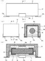
図1は本発明の第1実施形態のセメント抵抗器の概略を示し、図2はその詳細構造を断面図等により示す。一面を開放した箱体状のケース10の内部には、巻線抵抗器等の抵抗体20と、抵抗体20の周囲を取り囲むように配置した金属板30とが収容され、セメント材40により封止されている。巻線抵抗器等の抵抗体20は、その両端にキャップ21と、キャップ21に接続したリード端子22とからなる端子部材を備え、リード端子22のケース10から露出した部分は、ケースの開放面11側に面実装可能に加工され、開放面11と平行に配置された固定部分22aを備える。
FIG. 1 shows an outline of a cement resistor according to a first embodiment of the present invention, and FIG. 2 shows a detailed structure thereof by a sectional view and the like. Inside the box-
金属板30は、ケース10の内部で、抵抗体20と間隔を置いて、抵抗体20の周囲を取り囲むように配置されている。すなわち、金属板30は、ケースの底面(実装状態ではケースの上面)12と抵抗体20との間に配置された上面部分30aと、ケースの側面と抵抗体20との間に配置された側面部分30bとを備える。金属板のケースから露出した部分は、ケースの開放面11側に面実装可能に配置された固定部分(開放面11に沿って平行に外方に延びる実装面部分)30cを備える。
The
従って、図2(a)の正面図に示されるように、ケース10の実装面(ケースの開放面11)側には、リード端子22の面実装可能に配置された固定部分22aと、金属板30の面実装可能に配置された固定部分30cとを備え、これらは同一平面上に面実装が可能となるように配置されている。また、図2(c)(d)のとおり、セメント材40は、ケースの内部に、開放面11に到達しないように、充填されている。このため本発明品が回路基板に実装されたとき、リード端子22はセメント材に埋没した部分と固定部分22aとの間の部分において撓むことができるので、本発明品と回路基板との熱収縮による挙動を吸収することができ、長期にわたり安定した固定状態を維持することができる。これは金属板30においても同様である。
Therefore, as shown in the front view of FIG. 2 (a), on the mounting surface (
図3は、従来のセメント抵抗器の実装状態の温度分布のシミュレーション結果を示す。実装する印刷配線基板50には、抵抗器の電極用パッド(導電層)51を備え、抵抗器のリード端子の固定部分22aがはんだ接合により固定されている。なお、図3は左半分のみを示し、右半分は対称であるため、記載を省略している。また、温度分布は抵抗器の電極用パッド51の熱容量が十分に大きいと仮定し、その部分からの温度上昇を示す。
FIG. 3 shows a simulation result of a temperature distribution in a mounting state of a conventional cement resistor. The printed
シミュレーションでは、ケース10は40mm(L)×19mm(W)×15mm(H)のステアタイトを用い、長さ20mm、直径4mmのグラスロービング(ガラス芯)の周囲に0.5mm厚の抵抗体を配置し、充填材として結晶シリカを用い、定格電力5Wを供給した状態を示す。抵抗器の電極用パッド51の温度を基準とし、発熱量が最も大きい抵抗器中央部では80〜90℃程度迄温度が上昇し、ケース外表面では30〜60℃程度迄温度が上昇することが分かる。
In the simulation, the
これに対し、図4は本発明のセメント抵抗器の実装状態の温度分布のシミュレーション結果を示す。実装する印刷配線基板50には、抵抗器の電極用パッド51の他に放熱用パッド(金属層)52を備え、抵抗器のリード端子の固定部分22aが電極用パッド51に、金属板30の固定部分30cが放熱用パッド52にそれぞれはんだ接合により固定されている。
On the other hand, FIG. 4 shows the simulation result of the temperature distribution of the mounting state of the cement resistor of the present invention. The printed
なお、放熱用パッド52は、印刷配線基板50を貫通するサーマルビア54により印刷配線基板50の裏面側に設けたベタ電極パターン53に接続し、金属板30の冷却効果を高めるようにしている。また、金属板30を接続固定する放熱パッドを備えた熱伝導のよいアルミ基板やセラミック基板に実装した場合にも、高い放熱効果が得られる。この場合の放熱用パッドは単に基板上に設けたランドで良く、基板を貫通するサーマルビアは設けなくてもよい。
The
金属板30は、厚さ0.5mmの銅板を用い、上面部分30aが18mm(L)×11mm(W)であり、側面部分30bが18mm(L)×12.5mm(H)であり、固定部分30cが18mm(L)×4mm(W)である。上面部分30aおよび側面部分30bには、幅1mmで長さが全幅(W)または全高(H)に近いスリット(開口)が1mm間隔で、略全長(L)に渡って設けられている。
The
図4に示す温度分布のシミュレーション結果は、ケースの寸法、抵抗体の寸法および印加電力は、従来例と同じであるが、抵抗体20を取り囲むように配置した金属板30(上面部分30a、側面部分30b)により、抵抗体20の発熱が効果的に吸収され、固定部分30cから熱容量が十分に大きい放熱用パッド52に伝熱する。実際には、放熱用パッド52から、印刷配線基板50を貫通するサーマルビア54により印刷配線基板50の裏面側に設けたベタ電極パターン53に伝熱する等の冷却効果の高い配線パターンを採用することが好ましい。
The simulation result of the temperature distribution shown in FIG. 4 shows that the case dimensions, the resistor dimensions, and the applied power are the same as those in the conventional example, but the metal plate 30 (
これにより、大幅に抵抗体20の温度上昇を抑制することができ、抵抗体中央部でも30〜40℃程度に温度上昇を抑制することができ、ケース外表面では0〜10℃に温度上昇を抑制することができる。従って、金属板30が無い従来例と比較して、抵抗体内部で温度上昇は1/3程度に、ケース外表面では温度上昇は1/5程度に抑制することができる。このことは、同一寸法のセメント抵抗器において、金属板30を設け、印刷配線基板に設けた放熱用パッド(冷却用パッド)に接続することで、定格電力を3倍とすることができるうえ、ケース表面温度は従来品の定格電力時の温度上昇以下に抑えることが可能となると予想される。
Thereby, the temperature rise of the
さらに、セメント抵抗器において、金属板30を設け、印刷配線基板50に設けた放熱用パッド52に接続することで、セメント抵抗器の印刷配線基板への固着強度を向上することができる。すなわち、従来例では、セメント抵抗器と印刷配線基板とは、熱膨張係数が大きく異なり、セメント抵抗器の温度上昇により大きな熱応力が発生し、リード端子のはんだ接合部でクラックが発生するという問題がある。これに対し、本発明のセメント抵抗器では、金属板30の実装面部分30cを印刷配線基板の放熱用パッド52に接続することで、温度上昇を小さくでき熱応力を低減できるうえ、はんだ接合面積を大きくすることができ、固着強度を高め、実装の信頼性を高めることができる。
Furthermore, in the cement resistor, the
図5は、本発明の第2実施形態のセメント抵抗器を示す。この実施形態においても、一面を開放した箱体状のケース10の内部には、巻線抵抗器等の抵抗体20と、抵抗体20の周囲を取り囲むように配置した金属板30とが配置され、セメント材40により封止されていて、巻線抵抗器等の抵抗体20は、その両端にキャップ21と、キャップ21に接続したリード端子22とからなる端子部材を備える点は、第1実施形態と同様である。また、リード端子22のケース10から露出した部分は、ケースの開放面11側に面実装可能に、開放面11と平行に配置された部分を備える点も同様である。
FIG. 5 shows a cement resistor according to a second embodiment of the present invention. In this embodiment as well, a
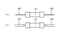
第1実施形態と相違するのは、ケースから露出した部分に、丸線のリード端子22をつぶして平板状にしたリード端子部分22dを備えた点である。すなわち、図6(a)は実装面(ケースの開放面)に平行な方向から見た図であり、図6(b)は実装面(ケースの開放面)に垂直な方向から見た図である。図示するように、リード端子22は、実装面(ケースの開放面)に垂直な方向につぶされ、実装面(ケースの開放面)に平行な方向に扁平となっている。これにより、リード端子22は、ケースの開放面11側に開放面と平行且つ扁平な部分を備え、丸棒と比較して面実装の接合面積を広げることができる。
The difference from the first embodiment is that a portion exposed from the case is provided with a
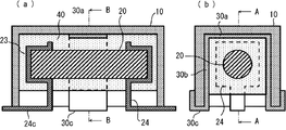
図7は、本発明の第3実施形態のセメント抵抗器を示す。この実施形態においても、一面を開放した箱体状のケース10の内部には、巻線抵抗器等の抵抗体20と、抵抗体20の周囲を取り囲むように配置した金属板30とが配置され、セメント材40により封止されていて、巻線抵抗器等の抵抗体20は、その両端にキャップ部23と、キャップ部23に接続した端子部材を備える点は、第1および第2実施形態と同様である。また、端子部材のケース10から露出した部分は、ケースの開放面11側に面実装可能に、開放面11と平行に配置された部分を備える点も同様である。また、金属板30は、ケースの底面(実装状態ではケースの上面)12と抵抗体20との間に配置された上面部分30aと、ケースの側面と抵抗体20との間に配置された側面部分30bとを備え、金属板のケース10から露出した部分は、ケースの開放面11側に面実装可能に配置された実装面部分30cとを備える点も、第1および第2実施形態と同様である。
FIG. 7 shows a cement resistor according to a third embodiment of the present invention. In this embodiment as well, a
この実施形態では、図8に示すように、板状端子部24とキャップ部23とを有する端子部材を抵抗体20の両端部に備えている。板状端子部24は折り曲げられ、端子部材のケース10から露出した部分は折り曲げ加工が施され、ケース10の開放した面側に面実装可能に配置された実装面部分24cを備える。ここで、板状端子部24とキャップ部23とは、図7(a)に示すように一体に金属材料により形成されている。従って、製造段階では、キャップ部23を抵抗体20の両端部に間挿し、キャップ部23の円筒部をかしめ、かしめ部23aを形成する(図9(a)参照)ことで、容易に端子部材を抵抗体20に装着することが可能である。
In this embodiment, as shown in FIG. 8, a terminal member having a plate-
この実施形態では、端子部材として、平板状の板状端子部24を用いるので、金属板30による熱伝導に加え、抵抗体20の両端からの熱伝導が増加し、実装基板への熱伝導性をさらに良好なものとすることができる。さらに印刷配線基板等の実装基板への固着性を向上することができる。なお、平板状の板状端子部24は、図9(b)に示すように、キャップ部23の直径よりも広幅の板状端子部24aを用いてもよい。これによりさらに実装基板への熱伝導性および固着性を高めることができる。
In this embodiment, since the flat plate-
次に、上記各種の実施形態に用いられる抵抗体の具体例について説明する。抵抗体20は、巻線抵抗器、皮膜抵抗器、セラミック抵抗器等の丸棒型の抵抗器や空芯コイル状の抵抗器など、各種の抵抗器を用いることができる。図10(a)は完成段階の巻線抵抗器の例を示し、図10(b)はその製造段階の例を示す。グラスロービングによりガラス芯20gを形成しつつ、NiCrまたはCuNi等の抵抗合金線を巻回し、所要の長さで切断し、ガラス芯20gの周囲に抵抗合金線を巻回した抵抗体20を製作する。そして、両端部にキャップ21を嵌め込み、かしめ加工によりかしめ部21aを形成し、キャップ21を抵抗体20に固定する。そして、リード線22をスポット溶接等によりキャップ21に固定することで、巻線抵抗器が完成する。
Next, specific examples of resistors used in the various embodiments will be described. As the
図11は、抵抗皮膜抵抗器の例を示し、図11(a)はトリミング前の状態を示し、図11(b)はトリミング後の状態を示す。この抵抗器は、まず円柱状のアルミナ等の碍子を準備し、その表面に抵抗皮膜を着膜する。抵抗皮膜としては、NiCr等の金属皮膜、SnO2等の酸化金属皮膜、カーボン等の炭素皮膜などがある。そして、両端部にキャップ21を嵌め込み、キャップ21を抵抗体20に固定し、リード端子22をスポット溶接等によりキャップ21に固定することで、抵抗皮膜抵抗器が完成する(図11(a)参照)。さらに、必要に応じてレーザまたはラバーカッタにてスパイラルトリミングを行い、抵抗値が調整された抵抗皮膜抵抗器が完成する(図11(b)参照)。また、抵抗ペーストを碍子の表面に塗布し、高温で焼成したメタルグレーズ抵抗器も利用が可能である。
FIG. 11 shows an example of a resistive film resistor, FIG. 11 (a) shows a state before trimming, and FIG. 11 (b) shows a state after trimming. This resistor first prepares a cylindrical insulator such as alumina and deposits a resistance film on the surface thereof. Examples of the resistance film include a metal film such as NiCr, a metal oxide film such as SnO 2 , and a carbon film such as carbon. Then, the
また、図11(a)の抵抗器と同じ外観を有する抵抗器として、セラミック抵抗器がある。これは、抵抗体20自体がバルクのセラミック抵抗体であり、両端部にキャップ21を嵌め込み、さらにリード線22をスポット溶接等により固定したものである。なお、セラミック抵抗体は、SnO2またはSbO2とタルクとを混練して成形後、高温で焼成することにより形成する。
Moreover, there exists a ceramic resistor as a resistor which has the same external appearance as the resistor of Fig.11 (a). In this case, the
図12は、セラミック芯巻線抵抗器の例を示す。この抵抗器は、円柱状のセラミック碍子20aの両端部にキャップ21を嵌め込み、NiCrまたはCuNi等の抵抗合金線の一端20cを一方のキャップ21に溶接により固定し、抵抗合金線20bを碍子20aに巻回し、抵抗合金線20bの他方の端部20cを他方のキャップ21に溶接により固定したものである。さらに、図示しないリード線等の端子部材をキャップ21に溶接等により固定する。
FIG. 12 shows an example of a ceramic core winding resistor. In this resistor, caps 21 are fitted into both ends of a cylindrical
また、セメント抵抗器用の抵抗体として、抵抗合金線をらせん状に巻回した空芯らせん状抵抗器を用いるようにしてもよい。この場合には、ケース内部の長手方向長さを有効に利用でき、且つ芯材およびキャップが不要であるので、低コストで熱放散性の良好な抵抗体が得られる。 Moreover, you may make it use the air core spiral resistor which wound the resistance alloy wire helically as a resistor for cement resistors. In this case, since the length in the longitudinal direction inside the case can be used effectively, and a core material and a cap are unnecessary, a resistor with good heat dissipation can be obtained at low cost.
次に、上記各種の実施形態に用いられる金属板の具体例について、図13を参照して説明する。(a)は基本的な構造例を示すもので、金属板30は、ケースの底面と抵抗体との間に配置される上面部分30aと、ケースの側面と抵抗体との間に配置される側面部分30bと、ケースの開放面に沿って平行に外方に延びる実装面部分30cとを備える。金属板30は、Cu等の熱伝導性の良好な金属材料を用いて製作される。これにより、抵抗体20と間隔を置いて、抵抗体20の周囲を取り囲むように金属板30をケース10内に配置し、金属板のケースから露出した部分は、ケースの開放した面側に面実装可能に配置された実装面部分30cを備えることから、実装基板側に導電性パターンを設け、該層に金属板の実装面部分を接続することで、金属板の部分30a,30bが抵抗体から吸収した熱を速やかに実装基板側に逃がすことができる。
Next, specific examples of the metal plate used in the various embodiments will be described with reference to FIG. (A) shows a basic structural example, and the
図13(b)は、(a)の改良例を示すもので、上面部30aが半円状をなしている。このため、半円状の金属板の軸芯に抵抗体の軸芯が位置するのであれば、抵抗体20と金属板30aとが同心状に配置されることになり、抵抗体と金属板との距離を略一定に保つことができ、金属板の吸熱効率を高めることができる。
FIG. 13B shows an improved example of FIG. 13A, and the
図13(c)は、(a)の改良例を示すもので、上面部分30aおよび側面部分30bに、スリット状の開口部30e,30dをそれぞれ設けたものである。開口部30e,30dを設けることで、セメント材を注入して封止する際に、セメント材を上面部分30aおよび側面部分30bの内部および裏側にスムーズに充填することができる。特に、金属板30の上面部分30aおよび側面部分30bとケースの内面との間にスペースができることを抑制することができる。
FIG. 13C shows an improved example of FIG. 13A, in which slit-shaped
さらに、開口部を設けることで、熱応力の分散が可能である。すなわち、銅などの金属板とセメント材とは、熱膨張係数が異なり、頻繁に膨張・収縮が繰り返されると、セメント材にクラックが生じ剥離等の問題が生じる恐れがある。しかしながら、開口部を設けることで開口部内にセメント材が充填され、熱応力を分散できることから、上記の問題の発生を防止することができる。 Furthermore, thermal stress can be dispersed by providing the opening. That is, the metal plate such as copper and the cement material have different coefficients of thermal expansion, and if expansion and contraction are frequently repeated, the cement material may crack and cause problems such as peeling. However, the provision of the opening fills the opening with a cement material and can disperse the thermal stress, thereby preventing the occurrence of the above problem.
しかしながら、開口部を設けることは、金属板内部で熱抵抗を増加させ、伝熱性を低下させる可能性がある。そこで、図13(d)に示すように、最も高温になる部分(抵抗体に最も近くなる部分)30f、30gに、開口部を設けないようにしたものである。すなわち、上面部分30aでは、開口30e,30eを分断するように、抵抗体20の長手方向に沿って開口部を設けない領域30fを設け、側面部分30bでは、開口30d,30dを分断するように抵抗体20の長手方向に沿って開口部を設けない領域30gを設けたものである。これにより、開口部を設けることでセメント材の良好な充填や熱応力の分散を可能とすると共に、最も高温になる部分(抵抗体に最も近くなる部分)30f、30gに開口部を設けないことで、抵抗体20からの良好な吸熱性を維持することができる。
However, providing the opening may increase the thermal resistance inside the metal plate and reduce the heat transfer property. Therefore, as shown in FIG. 13 (d), openings are not provided in the highest temperature portions (the portions closest to the resistor) 30f, 30g. That is, the
次に、上記各種の実施形態に用いられる箱体状のケースの具体例について、図14乃至図16を参照して説明する。図14に示すケースは、一面11を開放し、底面(実装時には上面となる)12を有する有底箱体状のケースであり、内部に段差等を設けないシンプルな構造のものである。ケースは、通常ステアタイトなどを用いて製作される。しかしながら、本発明のセメント抵抗器においては、抵抗体20を取り囲むように配置した金属板30を備えることで、金属板30の冷却効果によりケース部分の温度上昇は0〜10℃程度と僅かなものである(図4参照)。従って、プラスチック材料を用いたケースをセメント抵抗器に採用することが可能となり、プラスチック材料を用いることから、ケースの薄型化、高精度化、低コスト化が可能となる。プラスチック材料としては、PPEK、LCP、PPS等の熱可塑性樹脂(インジェクション成形)、エポキシ、フェノール等の熱硬化性樹脂(トランスファー成形)などを用いることができる。
Next, specific examples of the box-shaped case used in the various embodiments will be described with reference to FIGS. The case shown in FIG. 14 is a bottomed box-like case having one
図15に示すケースは、ケース10の長手方向両端面に、ケース10の開放面11から中央部に向けて延びる狭幅の切り欠き10kを設けたものである。切り欠き10kは、抵抗体20の両端のキャップ21の中央から垂直に延びるリード端子22を収容し、リード端子22をケース10から外部に導出するのに好適である(本発明の第2実施形態のセメント抵抗器(図5)を参照)。その他の点は、図14に示すケースと同様である。
The case shown in FIG. 15 is provided with a
図16に示すケースは、箱体状のケース10の両端面の内側に段部10mを設け、該段部10mに切り欠き10nを設けたものである。切り欠き10nは、抵抗体20の両端のキャップ21の中央から垂直に延びるリード端子22を折り曲げ、折り曲げた部分を収容するのに好適である(図2の本発明の第1実施形態のセメント抵抗器を参照)。なお、この実施形態では、折り曲げられたリード端子22は、切り欠き10nの壁面に沿ってケースの開放面11に対して垂直方向に延び、開放面11からケース外部に露出したところで再度折り曲げられ、開放面11に沿って平行にケースの両端面外側に延び、面実装可能に配置されている。
In the case shown in FIG. 16, a stepped
次に、本発明のセメント抵抗器の製造方法について、第1実施形態のセメント抵抗器を例として説明する。まず、図16に示す段部10mと切り欠き10nとを備えたケース10を準備する。そして、図15に示す上面部分30aと側面部分30bと実装面部分30cとを備えた金属板30を、ケース10の中央部に挿入し、実装面部分30cをケース10の側壁の上面に載置する。次に、リード端子22をケースの形状に合わせて折り曲げた抵抗器を、折り曲げ部が切り欠き10nに位置するように載置する。この時、金属板30の上面部分30aと側面部分30bとが抵抗体20を取り囲むように位置する。そして、アルミナ粉末やシリカ粉末を含むペースト状のセメント材を、ディスペンサを使って抵抗体20および金属板30を配置したケース内部に充填し、加温硬化によりセメント封止体を形成する。セメント材40はケースの開放面11に到達しないように充填される。そして、ケース外部に露出した金属部分に必要に応じてはんだ処理等を施して、セメント抵抗器が完成する。
Next, the cement resistor manufacturing method of the present invention will be described by taking the cement resistor of the first embodiment as an example. First, the
なお、上記実施形態では、金属板としてCu板を用いる例について説明したが、Cu板にNiメッキ、Snメッキを予め施しておくことが好ましい。Cuの酸化を抑制すると共に、実装面部分で実装基板とのハンダ接合性を良好なものとすることができる。また、Cu板以外にも、アルミ板、ステンレス鋼板等を用いることも可能である。 In the above embodiment, an example in which a Cu plate is used as the metal plate has been described. However, it is preferable that the Cu plate is preliminarily subjected to Ni plating and Sn plating. While suppressing the oxidation of Cu, the soldering property with the mounting substrate can be improved at the mounting surface portion. In addition to the Cu plate, an aluminum plate, a stainless steel plate or the like can be used.
これまで本発明の一実施形態について説明したが、本発明は上述の実施形態に限定されず、その技術的思想の範囲内において種々異なる形態にて実施されてよいことは言うまでもない。 Although one embodiment of the present invention has been described so far, it is needless to say that the present invention is not limited to the above-described embodiment, and may be implemented in various forms within the scope of the technical idea.
10 箱体状のケース
10k,10n 切り欠き
10m 段部
11 ケースの開放面
12 底面
20 抵抗体
20a 碍子
20b 抵抗合金線
20c 抵抗合金線の一端
20g ガラス芯
21 キャップ
22 リード端子
22d 扁平化したリード端子部分
23 キャップ部
23a かしめ部
24 板状端子部
24c 板状端子部の実装面部分
30 金属板
30a 金属板の上面部分
30b 金属板の側面部分
30c 金属板の固定部分(実装面部分)
30d,30e 開口部(スリット)
30f,30g 開口部を設けない領域
40 セメント材
50 印刷配線基板(実装基板)
51 電極用パッド
52 放熱用パッド
53 ベタ電極パターン
54 サーマルビア
DESCRIPTION OF
30d, 30e Opening (slit)
30f, 30g No
51
Claims (5)
該ケース内に配置した両端にキャップを備えた抵抗体と、
前記キャップに接続するとともに前記ケースから一部を露出させた一対の端子部材と、
前記ケース内に前記抵抗体と間隔を置いて前記抵抗体の周囲を取り囲むように配置するとともに前記ケースから一部を露出させた金属板と、
前記ケース内に充填したセメント材と、を備え、
前記端子部材の前記ケースからの露出部分と、前記金属板の前記ケースからの露出部分とを、前記ケースの開放面側の開放面に同一平面上に面実装可能に構成したことを特徴とするセメント抵抗器。 A box-shaped case with one side open,
A resistor provided with caps at both ends disposed in the case;
A pair of terminal members connected to the cap and partially exposed from the case;
A metal plate that is disposed so as to surround the resistor and spaced apart from the resistor in the case, and a part of the metal plate is exposed from the case;
A cement material filled in the case,
The exposed portion of the terminal member from the case and the exposed portion of the metal plate from the case are configured to be surface-mountable on the same open surface on the open surface side of the case. Cement resistor.
Priority Applications (1)
| Application Number | Priority Date | Filing Date | Title |
|---|---|---|---|
| JP2007202685A JP4982894B2 (en) | 2007-08-03 | 2007-08-03 | Cement resistor |
Applications Claiming Priority (1)
| Application Number | Priority Date | Filing Date | Title |
|---|---|---|---|
| JP2007202685A JP4982894B2 (en) | 2007-08-03 | 2007-08-03 | Cement resistor |
Publications (2)
| Publication Number | Publication Date |
|---|---|
| JP2009038275A JP2009038275A (en) | 2009-02-19 |
| JP4982894B2 true JP4982894B2 (en) | 2012-07-25 |
Family
ID=40439909
Family Applications (1)
| Application Number | Title | Priority Date | Filing Date |
|---|---|---|---|
| JP2007202685A Expired - Fee Related JP4982894B2 (en) | 2007-08-03 | 2007-08-03 | Cement resistor |
Country Status (1)
| Country | Link |
|---|---|
| JP (1) | JP4982894B2 (en) |
Families Citing this family (6)
| Publication number | Priority date | Publication date | Assignee | Title |
|---|---|---|---|---|
| JP2012119546A (en) * | 2010-12-02 | 2012-06-21 | Micron Electric Co Ltd | Connecting terminal and method for connecting electric element |
| EP2705530B1 (en) * | 2011-05-03 | 2018-07-04 | Vishay Dale Electronics, Inc. | Heat spreader for electrical components |
| JP6338359B2 (en) * | 2013-11-29 | 2018-06-06 | ミクロン電気株式会社 | Cement resistor |
| JP7042738B2 (en) | 2015-08-07 | 2022-03-28 | ヴィシェイ デール エレクトロニクス エルエルシー | Molds and electrical equipment with moldings for high voltage applications |
| JP6855991B2 (en) * | 2017-09-20 | 2021-04-07 | 株式会社デンソー | Resistor |
| CN113782284B (en) * | 2021-09-28 | 2022-11-29 | 深圳世纪稳特电子有限公司 | High-power cement resistor for frequency converter |
Family Cites Families (5)
| Publication number | Priority date | Publication date | Assignee | Title |
|---|---|---|---|---|
| JPH09148050A (en) * | 1995-11-29 | 1997-06-06 | Matsushita Electric Ind Co Ltd | Ptc heater |
| JP3870537B2 (en) * | 1998-03-05 | 2007-01-17 | 松下電器産業株式会社 | Resistor |
| JP3731108B2 (en) * | 2000-02-29 | 2006-01-05 | 三菱電機株式会社 | Resistor heat dissipation structure |
| JP2002290090A (en) * | 2001-03-28 | 2002-10-04 | Mitsumi Electric Co Ltd | Heat dissipation apparatus in substrate-packaging-type component |
| JP4846434B2 (en) * | 2006-05-09 | 2011-12-28 | コーア株式会社 | Cement resistor |
-
2007
- 2007-08-03 JP JP2007202685A patent/JP4982894B2/en not_active Expired - Fee Related
Also Published As
| Publication number | Publication date |
|---|---|
| JP2009038275A (en) | 2009-02-19 |
Similar Documents
| Publication | Publication Date | Title |
|---|---|---|
| JP4982894B2 (en) | Cement resistor | |
| JP5320612B2 (en) | Resistor | |
| KR101060013B1 (en) | Fuse Resistor, Manufacturing Method and Installation Method | |
| KR101038237B1 (en) | Thermal Fuse Resistor | |
| US20150287505A1 (en) | Resistor and manufacturing method thereof | |
| JP6491431B2 (en) | Fuse element and fuse element | |
| US10083780B2 (en) | Surface mount resistor | |
| CN108885928B (en) | Resistor with a resistor element | |
| CN111128493B (en) | Fuse resistor assembly and method of making same | |
| JP2007280919A (en) | Surface-mounted current fuse and its manufacturing method | |
| JP2572747Y2 (en) | 4 terminal power type surface mount resistor | |
| JPH0582002U (en) | Power type surface mount low resistor | |
| CN107871573B (en) | Fuse resistor and method for manufacturing the same | |
| JP6352350B2 (en) | Fuse resistor and manufacturing method thereof | |
| WO2017154546A1 (en) | Resistor | |
| JP2000260601A (en) | Resistor and method of producing the same | |
| JP5878651B2 (en) | Chip fuse and manufacturing method thereof | |
| WO2020202954A1 (en) | Electronic component mounting structure, and method for manufacturing electronic component mounting structure | |
| WO2023053594A1 (en) | Chip resistor | |
| JPH10229001A (en) | Surface-mounted type fixed resistor | |
| JPH06124801A (en) | Surface-mount type wire wound reistor | |
| JP2004335793A (en) | Thermometer | |
| JP2017054961A (en) | Resistor | |
| TWI600042B (en) | Fuse resistor and method of manufacturing the same | |
| JP3137482U (en) | Explosion-proof resistor |
Legal Events
| Date | Code | Title | Description |
|---|---|---|---|
| A621 | Written request for application examination |
Free format text: JAPANESE INTERMEDIATE CODE: A621 Effective date: 20100618 |
|
| A131 | Notification of reasons for refusal |
Free format text: JAPANESE INTERMEDIATE CODE: A131 Effective date: 20101005 |
|
| A521 | Written amendment |
Free format text: JAPANESE INTERMEDIATE CODE: A523 Effective date: 20101130 |
|
| A131 | Notification of reasons for refusal |
Free format text: JAPANESE INTERMEDIATE CODE: A132 Effective date: 20110705 |
|
| A521 | Written amendment |
Free format text: JAPANESE INTERMEDIATE CODE: A523 Effective date: 20110831 |
|
| TRDD | Decision of grant or rejection written | ||
| A01 | Written decision to grant a patent or to grant a registration (utility model) |
Free format text: JAPANESE INTERMEDIATE CODE: A01 Effective date: 20120403 |
|
| A01 | Written decision to grant a patent or to grant a registration (utility model) |
Free format text: JAPANESE INTERMEDIATE CODE: A01 |
|
| A61 | First payment of annual fees (during grant procedure) |
Free format text: JAPANESE INTERMEDIATE CODE: A61 Effective date: 20120406 |
|
| R150 | Certificate of patent or registration of utility model |
Ref document number: 4982894 Country of ref document: JP Free format text: JAPANESE INTERMEDIATE CODE: R150 Free format text: JAPANESE INTERMEDIATE CODE: R150 |
|
| FPAY | Renewal fee payment (event date is renewal date of database) |
Free format text: PAYMENT UNTIL: 20150511 Year of fee payment: 3 |
|
| R250 | Receipt of annual fees |
Free format text: JAPANESE INTERMEDIATE CODE: R250 |
|
| S533 | Written request for registration of change of name |
Free format text: JAPANESE INTERMEDIATE CODE: R313533 |
|
| R350 | Written notification of registration of transfer |
Free format text: JAPANESE INTERMEDIATE CODE: R350 |
|
| R250 | Receipt of annual fees |
Free format text: JAPANESE INTERMEDIATE CODE: R250 |
|
| R250 | Receipt of annual fees |
Free format text: JAPANESE INTERMEDIATE CODE: R250 |
|
| R250 | Receipt of annual fees |
Free format text: JAPANESE INTERMEDIATE CODE: R250 |
|
| R250 | Receipt of annual fees |
Free format text: JAPANESE INTERMEDIATE CODE: R250 |
|
| R250 | Receipt of annual fees |
Free format text: JAPANESE INTERMEDIATE CODE: R250 |
|
| LAPS | Cancellation because of no payment of annual fees |