JP4982686B2 - Circuit for generating overdriver control signal of semiconductor memory device - Google Patents
Circuit for generating overdriver control signal of semiconductor memory device Download PDFInfo
- Publication number
- JP4982686B2 JP4982686B2 JP2005189039A JP2005189039A JP4982686B2 JP 4982686 B2 JP4982686 B2 JP 4982686B2 JP 2005189039 A JP2005189039 A JP 2005189039A JP 2005189039 A JP2005189039 A JP 2005189039A JP 4982686 B2 JP4982686 B2 JP 4982686B2
- Authority
- JP
- Japan
- Prior art keywords
- signal
- output
- overdriving
- overdriver
- gate
- Prior art date
- Legal status (The legal status is an assumption and is not a legal conclusion. Google has not performed a legal analysis and makes no representation as to the accuracy of the status listed.)
- Expired - Fee Related
Links
- 239000004065 semiconductor Substances 0.000 title claims description 20
- 230000004044 response Effects 0.000 claims description 25
- 230000003111 delayed effect Effects 0.000 claims description 12
- 230000007274 generation of a signal involved in cell-cell signaling Effects 0.000 claims description 6
- 238000010586 diagram Methods 0.000 description 7
- 238000000034 method Methods 0.000 description 6
- 238000000926 separation method Methods 0.000 description 6
- 101100286980 Daucus carota INV2 gene Proteins 0.000 description 5
- 101100508840 Daucus carota INV3 gene Proteins 0.000 description 5
- 101100397045 Xenopus laevis invs-b gene Proteins 0.000 description 5
- HCUOEKSZWPGJIM-YBRHCDHNSA-N (e,2e)-2-hydroxyimino-6-methoxy-4-methyl-5-nitrohex-3-enamide Chemical compound COCC([N+]([O-])=O)\C(C)=C\C(=N/O)\C(N)=O HCUOEKSZWPGJIM-YBRHCDHNSA-N 0.000 description 3
- 101001109689 Homo sapiens Nuclear receptor subfamily 4 group A member 3 Proteins 0.000 description 3
- 101000598778 Homo sapiens Protein OSCP1 Proteins 0.000 description 3
- 101001067395 Mus musculus Phospholipid scramblase 1 Proteins 0.000 description 3
- 102100022673 Nuclear receptor subfamily 4 group A member 3 Human genes 0.000 description 3
- 101150110971 CIN7 gene Proteins 0.000 description 2
- 101150110298 INV1 gene Proteins 0.000 description 2
- 101100397044 Xenopus laevis invs-a gene Proteins 0.000 description 2
- 101150070189 CIN3 gene Proteins 0.000 description 1
- 241000255777 Lepidoptera Species 0.000 description 1
- 230000001934 delay Effects 0.000 description 1
- 238000012986 modification Methods 0.000 description 1
- 230000004048 modification Effects 0.000 description 1
Images


Classifications
-
- G—PHYSICS
- G11—INFORMATION STORAGE
- G11C—STATIC STORES
- G11C7/00—Arrangements for writing information into, or reading information out from, a digital store
- G11C7/12—Bit line control circuits, e.g. drivers, boosters, pull-up circuits, pull-down circuits, precharging circuits, equalising circuits, for bit lines
-
- G—PHYSICS
- G11—INFORMATION STORAGE
- G11C—STATIC STORES
- G11C7/00—Arrangements for writing information into, or reading information out from, a digital store
- G11C7/06—Sense amplifiers; Associated circuits, e.g. timing or triggering circuits
- G11C7/08—Control thereof
-
- G—PHYSICS
- G11—INFORMATION STORAGE
- G11C—STATIC STORES
- G11C11/00—Digital stores characterised by the use of particular electric or magnetic storage elements; Storage elements therefor
- G11C11/21—Digital stores characterised by the use of particular electric or magnetic storage elements; Storage elements therefor using electric elements
- G11C11/34—Digital stores characterised by the use of particular electric or magnetic storage elements; Storage elements therefor using electric elements using semiconductor devices
- G11C11/40—Digital stores characterised by the use of particular electric or magnetic storage elements; Storage elements therefor using electric elements using semiconductor devices using transistors
- G11C11/401—Digital stores characterised by the use of particular electric or magnetic storage elements; Storage elements therefor using electric elements using semiconductor devices using transistors forming cells needing refreshing or charge regeneration, i.e. dynamic cells
- G11C11/4063—Auxiliary circuits, e.g. for addressing, decoding, driving, writing, sensing or timing
- G11C11/407—Auxiliary circuits, e.g. for addressing, decoding, driving, writing, sensing or timing for memory cells of the field-effect type
- G11C11/409—Read-write [R-W] circuits
- G11C11/4091—Sense or sense/refresh amplifiers, or associated sense circuitry, e.g. for coupled bit-line precharging, equalising or isolating
-
- G—PHYSICS
- G11—INFORMATION STORAGE
- G11C—STATIC STORES
- G11C5/00—Details of stores covered by group G11C11/00
- G11C5/14—Power supply arrangements, e.g. power down, chip selection or deselection, layout of wirings or power grids, or multiple supply levels
Landscapes
- Engineering & Computer Science (AREA)
- Microelectronics & Electronic Packaging (AREA)
- Computer Hardware Design (AREA)
- Power Engineering (AREA)
- Dram (AREA)
- Static Random-Access Memory (AREA)
Description
本発明は、半導体の設計技術に関し、特に、半導体メモリ素子のビットラインオーバードライビング方式に関し、より詳しくは、オーバードライバを制御するオーバードライビングパルスを生成するための回路に関する。 The present invention relates to a semiconductor design technique, and more particularly to a bit line overdriving method of a semiconductor memory device, and more particularly to a circuit for generating an overdriving pulse for controlling an overdriver.
一般に、半導体メモリチップを構成する線幅及びセルサイズの持続的なスケーリングダウンが進むにつれ、電源電圧の低電圧化が加速し、これによって低電圧の環境で要求される性能を満足させるための設計技術が求められている。 In general, as the line width and cell size of a semiconductor memory chip are continuously scaled down, the power supply voltage is lowered and the design for satisfying the performance required in the low voltage environment is accelerated. Technology is required.
現在、大部分の半導体メモリチップは、外部電圧(電源電圧)を印加されて内部電圧を発生させるための内部電圧発生回路をチップ内に搭載してチップ内部回路の動作に必要な電圧を自ら供給するようにしている。その中でも、DRAMのようにビットライン感知増幅器を用いるメモリ素子の場合、セルデータを感知するためにコア電圧VCOREを用いている。 Currently, most semiconductor memory chips have an internal voltage generation circuit for generating an internal voltage when an external voltage (power supply voltage) is applied, and supply the voltage necessary for the operation of the chip's internal circuit. Like to do. Among them, in the case of a memory device using a bit line sense amplifier such as a DRAM, the core voltage VCORE is used to sense cell data.
ローアドレスによって選択されたワードラインが活性化されると、そのワードラインに接続されている複数のメモリセルのデータがビットラインに伝達され、ビットライン感知増幅器はビットライン対の電圧差を感知及び増幅する。このような数千個のビットライン感知増幅器が一気に動作するようになるが、この時、ビットライン感知増幅器のRTO電源ラインを駆動するのに用いられるコア電圧端VCOREから多い量の電流が消費される。ところが、動作電圧が低くなる状況でコア電圧VCOREを用いて短い時間に多くのセルのデータを増幅するには困難がある。 When a word line selected by a row address is activated, data of a plurality of memory cells connected to the word line is transmitted to the bit line, and a bit line sense amplifier senses a voltage difference between the bit line pair. Amplify. Thousands of bit line sense amplifiers operate at once, but at this time, a large amount of current is consumed from the core voltage terminal VCORE used to drive the RTO power line of the bit line sense amplifier. The However, it is difficult to amplify data of many cells in a short time using the core voltage VCORE in a situation where the operating voltage is low.
このような問題点を解決するために、ビットライン感知増幅器の動作初期(メモリセルとビットライン間の電荷共有の直後)にビットライン感知増幅器のRTO電源ラインを一定時間の間にコア電圧VCOREよりも高い電圧(通常、電源電圧VDD)で駆動するビットライン感知増幅器オーバードライビング方式を採用することとなった。 In order to solve such a problem, the RTO power line of the bit line sense amplifier is connected to the core voltage VCORE for a certain time in the initial operation of the bit line sense amplifier (immediately after the charge sharing between the memory cell and the bit line). The bit line sense amplifier overdriving method, which is driven by a higher voltage (usually the power supply voltage VDD), is adopted.
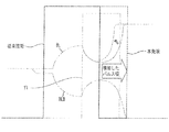
図1は、オーバードライビング方式を採用したビットライン感知増幅器アレイの構成を示す図である。 FIG. 1 is a diagram illustrating a configuration of a bit line sense amplifier array employing an overdriving method.
図1を参照すれば、ビットライン感知増幅器アレイは、オーバードライビングを採用しているか否かに関係なくビットライン感知増幅器30と、上位ビットライン分離部10及び下位ビットライン分離部50と、ビットラインイコライズ/プリチャージ部20と、カラム選択部40と、ビットライン感知増幅器電源ライン駆動部60とを含む。
Referring to FIG. 1, the bit line sense amplifier array includes a bit
ここで、上位ビットライン分離部10は、上位分離信号BISHに応答して上位メモリセルアレイと感知増幅器30とを分離/接続するためのもので、下位ビットライン分離部50は、下位分離信号BISLに応答して下位メモリセルアレイと感知増幅器30とを分離/接続するためのものである。
Here, the upper bit
そして、ビットライン感知増幅器30はイネーブル信号が活性化されてSB電源ライン及びRTO電源ラインが、予定された電圧レベルで駆動されるとビットライン対BL、BLB(電荷共有状態で微細な電圧差を有する)の電圧差を感知して、1つは接地電圧VSSで、もう1つはコア電圧VCOREで増幅する。
When the enable signal is activated and the SB power line and the RTO power line are driven at a predetermined voltage level, the bit
また、ビットラインイコライズ/プリチャージ部20は、ビットラインに対する感知/増幅及び再格納の過程を終了した後にビットラインイコライズ信号BLEQに応答してビットライン対BL、BLBをビットラインプリチャージ電圧VBLP(通常、VCORE/2)にプリチャージするためのものである。
In addition, the bit line equalize /
そして、カラム選択部40はリードコマンドが印加されると、カラム選択信号YIに応答して感知増幅器30により感知/増幅されたデータをセグメントデータバスSIO、SIOBに伝達する。
When the read command is applied, the
一方、ビットライン感知増幅器電源ライン駆動部60は、第1電源ライン駆動制御信号SAPに応答してコア電圧端VCOREにかかっている電圧でRTO電源ラインを駆動するための第1ノーマルドライバトランジスタM2と、第2電源ライン駆動制御信号SANに応答して接地電圧VSSでSB電源ラインを駆動するための第2ノーマルドライバトランジスタM3と、アクティブコマンドを受けて生成されたオーバードライビング信号OVDを印加されてオーバードライビングパルスSAOVDP(オーバードライバ制御信号)を生成するためのオーバードライビングパルス生成部64と、オーバードライビングパルスSAOVDPに応答してコア電圧端VCOREを電源電圧VDDで駆動するためのオーバードライバトランジスタM1と、ビットラインイコライズ信号BLEQに応答してビットライン感知増幅器30のRTO電源ライン及びSB電源ラインをビットラインプリチャージ電圧VBLPにプリチャージするためのビットライン感知増幅器電源ラインイコライズ/プリチャージ部62とを備える。
Meanwhile, the bit line sense amplifier
ここでは、オーバードライビングパルスSAOVDPをハイアクティブパルスと規定し、オーバードライバトランジスタM1をNMOSトランジスタで具現する場合を例示しているが、プルアップ駆動により一層有利なPMOSトランジスタを用いることもできる。 In this example, the over driving pulse SAOVDP is defined as a high active pulse, and the over driver transistor M1 is implemented as an NMOS transistor. However, a PMOS transistor that is more advantageous by pull-up driving can be used.
図2は、前記図1に係る動作波形を示している。 FIG. 2 shows operation waveforms according to FIG.
図2を参照すれば、まずアクティブコマンドが印加されてワードラインが活性化され、セルに格納されているデータが電荷共有によりビットライン対BL、BLBにそれぞれ誘起された後、一定時間後に第1及び第2電源ライン駆動制御信号SAP、SANが論理レベルハイに活性化される。この時、アクティブコマンドを受けて第1及び第2電源ライン駆動制御信号SAP、SANよりも先に論理レベルハイに活性化されているオーバードライビングパルスSAOVDPによりRTO電源ラインがオーバードライビングされる。すなわち、第1及び第2電源ライン駆動制御信号SAP、SAN、オーバードライビングパルスSAOVDPが何れも論理レベルハイに活性化されると、トランジスタM1、M2、M3が何れもターンオンされてRTO電源ラインを電源電圧VDDで駆動し、SB電源ラインを接地電圧VSSで駆動する。 Referring to FIG. 2, first, an active command is applied to activate a word line, and data stored in a cell is induced in the bit line pair BL and BLB by charge sharing, and then a first time later. The second power line drive control signals SAP and SAN are activated to a logic level high. At this time, the RTO power supply line is overdriven by the overdriving pulse SAOVDP which is activated to the logic level high prior to the first and second power supply line drive control signals SAP and SAN in response to the active command. That is, when the first and second power line drive control signals SAP and SAN and the overdriving pulse SAOVDP are all activated to a logic level high, the transistors M1, M2 and M3 are all turned on to power the RTO power line. It is driven by the voltage VDD, and the SB power line is driven by the ground voltage VSS.
その後、一定時間が経過すれば、オーバードライビングパルスSAOVDPが論理レベルローに非活性化されてRTO電源ラインをコア電圧VCOREで駆動するようになる。 Thereafter, when a certain period of time elapses, the over driving pulse SAOVDP is deactivated to a logic level low, and the RTO power supply line is driven with the core voltage VCORE.
ところが、図2に示すように、オーバードライビング区間でリードコマンドが入力される場合、このリードコマンドを受けてカラム選択信号YIが論理レベルハイに活性化される。このようにオーバードライビングが行われる間にカラム選択信号YIが活性化される場合、ビットラインBL、BLBとセグメントデータバスSIO、SIOBが接続されながら電荷共有が発生し、これによってビットラインBL、BLBのレベルが急激にダウンする現象が起きる。 However, as shown in FIG. 2, when a read command is input in the overdriving period, the column selection signal YI is activated to the logic level high in response to this read command. When the column selection signal YI is activated during overdriving as described above, charge sharing occurs while the bit lines BL and BLB are connected to the segment data buses SIO and SIOB, and thereby the bit lines BL and BLB are connected. The phenomenon that the level of the abruptly goes down occurs.
もし、この状態でカラム選択信号YIが、まだ論理レベルローに非活性化されていない状況でオーバードライビングパルスSAOVDPが論理レベルローに非活性化されてオーバードライビングが終了すれば、ビットラインBLの電位が、ターゲットレベルであるコア電圧VCOREレベルに達するには相対的に多くの時間がかかってしまう。すなわち、オーバードライビングの効率が低下する。 If the overdriving pulse SAOVDP is deactivated to the logic level low in the state where the column selection signal YI is not yet deactivated to the logic level low in this state, the potential of the bit line BL is terminated. However, it takes a relatively long time to reach the core voltage VCORE level which is the target level. That is, overdriving efficiency is reduced.
この場合、再格納のような後続動作のタイミングマージンが減少するという問題点があり、セグメントデータバスSIO、SIOBに相対的に低いレベルの電位が伝達されてデータバス感知マージンを低下させる恐れがある。
本発明は、上記した従来技術の問題点に鑑みてなされたものであって、その目的とするところは、オーバードライビング区間で印加されるリードコマンドによるオーバードライビング効率の低下を防止できる半導体メモリ素子のオーバードライバ制御信号の生成回路を提供することにある。 The present invention has been made in view of the above-described problems of the prior art, and an object of the present invention is to provide a semiconductor memory device that can prevent a decrease in overdriving efficiency due to a read command applied in an overdriving section. An object of the present invention is to provide an overdriver control signal generation circuit.
上記目的を達成するために本発明の第1観点による半導体メモリ素子のオーバードライバ制御信号の生成回路は、アクティブコマンドを受けて生成されたオーバードライビング信号を印加されてビットラインオーバードライバ制御信号を生成するための半導体メモリ素子のオーバードライバ制御信号の生成回路において、前記オーバードライビング信号を遅延させて出力するための遅延手段と、オーバードライビング信号及びリードコマンド信号に応答して前記遅延手段から遅延されたオーバードライビング信号がそのまま出力されるか、ディセーブルされて出力されるように制御するための制御手段と、前記オーバードライビング信号に、前記遅延手段の出力信号による所定のパルス幅を追加するためのパルス幅追加手段とを備えることを特徴とする。 To achieve the above object, an overdriver control signal generation circuit for a semiconductor memory device according to a first aspect of the present invention generates a bit line overdriver control signal by applying an overdriving signal generated in response to an active command. In a circuit for generating an overdriver control signal of a semiconductor memory device for delaying, a delay means for delaying and outputting the overdriving signal, and being delayed from the delay means in response to the overdriving signal and the read command signal A control means for controlling the overdriving signal to be output as it is or disabled and a pulse for adding a predetermined pulse width according to the output signal of the delay means to the overdriving signal Width adding means And butterflies.
また、本発明の第2観点による半導体メモリ素子のオーバードライバ制御信号の生成回路は、アクティブコマンドを受けて生成されたオーバードライビング信号を印加されてビットラインオーバードライバ制御信号を生成するための半導体メモリ素子のオーバードライバ制御信号の生成回路において、カラム選択信号のパルシング情報を提供するためのパルシング情報提供手段と、前記オーバードライビング信号、リードコマンド信号及びプリチャージコマンド信号に応答して前記パルシング情報提供手段から前記カラム選択信号に対応する信号がパルス幅を維持して出力されるか、ディセーブルされて出力されるように制御するための制御手段と、前記オーバードライビング信号に、前記パルシング情報提供手段の出力信号による所定のパルス幅を追加して前記ビットラインオーバードライバ制御信号に出力するためのパルス幅追加手段とを備えることを特徴とする。 A circuit for generating an overdriver control signal for a semiconductor memory device according to a second aspect of the present invention is a semiconductor memory for generating a bit line overdriver control signal by applying an overdriving signal generated in response to an active command. In a device overdriver control signal generation circuit, pulsing information providing means for providing pulsing information of a column selection signal, and the pulsing information providing means in response to the overdriving signal, read command signal and precharge command signal From the control means for controlling the signal corresponding to the column selection signal to be output with the pulse width maintained or disabled, and to the overdriving signal, the pulsing information providing means Predetermined performance by output signal Characterized in that by adding the scan width and a pulse width added means for outputting to the bit lines over driver control signal.
本発明では、ビットラインオーバードライビングが行われる状態でリードコマンドが印加される場合、オーバードライバ制御信号のパルス幅を増大させることによってカラム選択信号が活性化された状態でオーバードライバ制御信号が非活性化されることによるオーバードライビング効率の低下を防止できる。そのためには、ビットラインオーバードライビングが行われる状態でリードコマンドが印加されるのを感知し、それに応じてオーバードライバ制御信号のパルス幅が選択的に拡張されるように制御できる構造が必要となるが、ここで遅延されたオーバードライビング信号(コマンド信号を受けて生成されるオーバードライバ制御信号のソース信号である)を用いるか、カラム選択信号を用いることができる。 In the present invention, when a read command is applied in a state where bit line overdriving is performed, the overdriver control signal is deactivated while the column selection signal is activated by increasing the pulse width of the overdriver control signal. Therefore, it is possible to prevent a decrease in overdriving efficiency due to being made. For this purpose, it is necessary to have a structure capable of sensing that a read command is applied in a state where bit line overdriving is performed and controlling the pulse width of the overdriver control signal to be selectively expanded accordingly. However, it is possible to use a delayed overdriving signal (which is a source signal of an overdriver control signal generated by receiving a command signal) or a column selection signal.
本発明は、オーバードライビングが行われる状態でリードコマンドが印加される場合、オーバードライバ制御信号のパルス幅を拡張させることでオーバードライビングの効率が低下するのを防止でき、これによってオーバードライビング後の後続動作のタイミングマージン及びデータバス感知マージンを確保できるという効果を奏する。 According to the present invention, when a read command is applied in a state where overdriving is performed, it is possible to prevent the efficiency of overdriving from being reduced by extending the pulse width of the overdriver control signal, and thereby the subsequent after overdriving. The operation timing margin and the data bus sensing margin can be ensured.
以下、添付する図面を参照しつつ本発明の最も好ましい実施の形態を説明する。 Hereinafter, the most preferred embodiment of the present invention will be described with reference to the accompanying drawings.
図3は、本発明の一実施の形態に係る半導体メモリ素子のオーバードライビングパルス生成回路を示す図である。 FIG. 3 is a diagram illustrating an overdriving pulse generation circuit for a semiconductor memory device according to an embodiment of the present invention.
図3を参照すれば、本実施の形態に係るオーバードライビングパルスの生成回路は、オーバードライビング信号OVDを遅延させて出力するための遅延部310と、オーバードライビング信号OVD、リードコマンド信号RD及びプリチャージコマンド信号PCGに応答して遅延部310から遅延オーバードライビング信号OVD1がそのまま出力されるか、ディセーブルされて出力されるように制御するための制御部320と、オーバードライビング信号OVDに遅延部310から出力される遅延オーバードライビング信号OVD1による所定のパルス幅を追加してオーバードライビングパルスSAOVDPとして出力するためのパルス幅追加部330とを備える。
Referring to FIG. 3, the overdriving pulse generating circuit according to the present embodiment includes a delay unit 310 for delaying and outputting an overdriving signal OVD, an overdriving signal OVD, a read command signal RD, and a precharge. In response to the command signal PCG, the delay unit 310 outputs the delayed overdriving signal OVD1 as it is or disables the overdriving signal OVD from being output from the delay unit 310. A pulse
ここで、遅延部310は、オーバードライビング信号OVDを入力されて一定時間だけ遅延させて遅延オーバードライビング信号OVD1を出力するためのディレイ315と、ディレイ315の出力信号を反転させるためのインバータINV1と、インバータINV1の出力信号及び制御部320の出力信号を入力とするNORゲートNOR1とを備える。
Here, the delay unit 310 receives the overdriving signal OVD and delays it for a predetermined time to output the delayed overdriving signal OVD1, and an inverter INV1 for inverting the output signal of the
また、制御部320は、リードコマンド信号RD及びオーバードライビング信号OVDを入力とするNANDゲートNAND1と、NANDゲートNAND1の出力信号をゲート入力とするプルアップPMOSトランジスタMP1と、プリチャージコマンド信号PCGをゲート入力とするプルダウンNMOSトランジスタMN1と、プルアップPMOSトランジスタMP1及びプルダウンNMOSトランジスタMN1から構成されたバッファの出力端(ノードN1)に接続されているインバータラッチINV2、INV3と、電源電圧端VDDとインバータラッチINV2、INV3の出力端(ノードN2)(制御部320の出力端)との間に接続され、パワーアップ信号PWRUPをゲート入力とする初期化PMOSトランジスタMP2とを備える。
The
そして、パルス幅追加部330は、遅延オーバードライビング信号OVD1及び遅延部310の出力信号を入力とするNORゲートNOR2と、NORゲートNOR2の出力信号を反転させてオーバードライビングパルスSAOVDPとして出力するためのインバータINV4とを備える。
The pulse
図4は、前記図3のオーバードライビングパルス生成回路のタイミング図である。 FIG. 4 is a timing diagram of the overdriving pulse generation circuit of FIG.
図4を参照すれば、まずチップにパワーが印加されてパワーアップ信号PWRUPが論理レベルローにパルシングされると、制御部320の初期化PMOSトランジスタMP2がターンオンされてインバータラッチINV2、INV3の出力端(ノードN2)が論理レベルハイに初期化される。これによって遅延部310のNORゲートNOR1がディセーブルされて遅延部310の出力信号である遅延オーバードライビング信号OVD1は論理レベルローの状態を維持するため、パルス幅追加部330はオーバードライビング信号OVDをそのままオーバードライビングパルスSAOVDPとして出力する。
Referring to FIG. 4, when power is first applied to the chip and the power-up signal PWRUP is pulsed to a logic level low, the initialization PMOS transistor MP2 of the
一方、アクティブコマンドが印加され、これを受けてオーバードライビング信号OVDが論理レベルハイに活性化され、その後、第1及び第2電源ライン駆動制御信号SAP、SAN(前記図1参照)が活性化されてオーバードライビングが開始される。 On the other hand, an active command is applied and the overdriving signal OVD is activated to a logic level high in response to this, and then the first and second power line drive control signals SAP and SAN (see FIG. 1) are activated. Overdriving starts.
このように、オーバードライビングが行われる状態でリードコマンドが印加されてリードコマンド信号RDが論理レベルハイに活性化されると、制御部320のNANDゲートNAND1の出力は論理レベルローになってプルアップPMOSトランジスタMP1がターンオンされ、インバータラッチINV2、INV3のラッチ値が変わって制御部320の出力信号は論理レベルローとなる。
As described above, when the read command is applied in the overdriving state and the read command signal RD is activated to the logic level high, the output of the NAND gate NAND1 of the
このような論理レベルローの制御部320の出力信号を入力として受ける遅延部310のNORゲートNOR1は、インバータのように動作するため、遅延部310は論理レベルハイに活性化された状態のオーバードライビング信号OVDを遅延させて出力するようになる。結局、パルス幅追加部330は元のオーバードライビング信号OVDと、遅延部320から出力された遅延オーバードライビング信号OVD1とを論理和して元のオーバードライビング信号OVDに比べてパルス幅(論理レベルハイ区間)が拡張されたオーバードライビングパルスSAOVDPを出力する(図4のA部分)。
The NOR gate NOR1 of the delay unit 310 that receives the output signal of the logic level
その後、プリチャージコマンドが印加されてプリチャージコマンド信号PCGが論理レベルハイになると、制御部320のプルダウンNMOSトランジスタPCGがターンオンされて制御部320の出力信号が再び初期値である論理レベルハイに復帰する。
Thereafter, when a precharge command is applied and the precharge command signal PCG becomes a logic level high, the pull-down NMOS transistor PCG of the
一方、図4のB部分のように、リードコマンド信号RDとオーバードライビング区間がオーバーラップされない場合には、リードコマンドが印加されてもインバータラッチINV2、INV3のラッチ値が変わらないため、オーバードライビングパルスSAOVDPはオーバードライビング信号OVDと同様のパルス幅を示す。 On the other hand, when the read command signal RD and the overdriving section do not overlap as shown in the B part of FIG. 4, the latch values of the inverter latches INV2 and INV3 do not change even when the read command is applied. SAOVDP shows the same pulse width as that of the overdriving signal OVD.
以上、説明したように、本実施の形態を適用すれば、オーバードライビングが行われる状態でリードコマンドが印加されてリードコマンド信号RDが論理レベルハイに活性化される場合にも、前記図2に示すように、オーバードライビングパルスSAOVDPのパルス幅の拡張により、カラム選択信号YI(リードコマンドを受けて生成される)が論理レベルハイに活性化された状態でオーバードライビングパルスSAOVDPが論理レベルローに非活性化されることを防止できる。すなわち、オーバードライビングの効率が低下するのを防止できる。 As described above, if the present embodiment is applied, the read command is applied in the state where overdriving is performed and the read command signal RD is activated to the logic level high as shown in FIG. As shown, the overdriving pulse SAOVDP is not driven to a logic level low while the column selection signal YI (generated in response to the read command) is activated to a logic level high by extending the pulse width of the overdriving pulse SAOVDP. It can be prevented from being activated. That is, it is possible to prevent the overdriving efficiency from being lowered.
図5は、本発明の他の実施の形態に係る半導体メモリ素子のオーバードライビングパルス生成回路を示す図である。 FIG. 5 is a diagram illustrating an overdriving pulse generation circuit of a semiconductor memory device according to another embodiment of the present invention.
図5を参照すれば、本実施の形態に係るオーバードライビングパルスの生成回路は、カラム選択信号YIのパルシング情報を提供するためのパルシング情報提供部510と、オーバードライビング信号OVD、リードコマンド信号RD及びプリチャージコマンド信号PCGに応答してパルシング情報提供部510からカラム選択信号YIに対応する信号がパルス幅を維持して出力されるか、ディセーブルされて出力されるように制御するための制御部520と、オーバードライビング信号OVDにパルシング情報提供部510の出力信号による所定のパルス幅を追加してオーバードライビングパルスSAOVDPに出力するためのパルス幅追加部530とを備える。
Referring to FIG. 5, the overdriving pulse generating circuit according to the present embodiment includes a pulsing
ここで、パルシング情報提供部510は、カラム選択信号YIを入力とするインバータINV1_Aと、インバータINV1_Aの出力信号及び制御部520の出力信号を入力とするNORゲートNOR1_Aとを備える。
Here, the pulsing
また、制御部520は、リードコマンド信号RD及びオーバードライビング信号OVDを入力とするNANDゲートNAND1_Aと、NANDゲートNAND1_Aの出力信号をゲート入力とするプルアップPMOSトランジスタMP1_Aと、プリチャージコマンド信号PCGをゲート入力とするプルダウンNMOSトランジスタMN1_Aと、プルアップPMOSトランジスタMP1_A及びプルダウンNMOSトランジスタMN1_Aから構成されたバッファの出力端(ノードN1_A)に接続されているインバータラッチINV2_A、INV3_Aと、電源電圧端VDDとインバータラッチINV2_A、INV3_Aの出力端(ノードN2_A)(制御部520の出力端)との間に接続され、パワーアップ信号PWRUPをゲート入力とする初期化PMOSトランジスタMP2_Aとを備える。
The
そして、パルス幅追加部530は、オーバードライビング信号OVD及びパルシング情報提供部510の出力信号を入力とするNORゲートNOR2_Aと、NORゲートNOR2_Aの出力信号を反転させてオーバードライビングパルスSAOVDPとして出力するためのインバータINV4_Aとを備える。
Then, the pulse
すなわち、上述した一実施の形態では、特定区間でオーバードライビング信号OVDに比べてパルス幅(論理レベルハイ区間)が拡張されたオーバードライビングパルスSAOVDPを生成するために、遅延されたオーバードライビング信号を用いたのに対して、本実施の形態ではリードコマンドの印加時に活性化されるカラム選択信号YIを用いた。 That is, in the above-described embodiment, a delayed overdriving signal is used to generate an overdriving pulse SAOVDP in which a pulse width (logic level high section) is expanded compared to the overdriving signal OVD in a specific section. In contrast, in this embodiment, a column selection signal YI that is activated when a read command is applied is used.
図6は、前記図5のオーバードライビングパルス生成回路のタイミング図である。 FIG. 6 is a timing diagram of the overdriving pulse generation circuit of FIG.
図6を参照すれば、まずチップにパワーが印加されてパワーアップ信号PWRUPが論理レベルローにパルシングされると、制御部520の初期化PMOSトランジスタMP2_AがターンオンされてインバータラッチINV2_A、INV3_Aの出力端(ノードN2_A)が論理レベルハイに初期化される。これによって、パルシング情報提供部510のNORゲートNOR1_Aがディセーブルされてパルシング情報提供部510の出力信号は論理レベルローの状態を維持するようになるため、パルス幅追加部530はオーバードライビング信号OVDをそのままオーバードライビングパルスSAOVDPとして出力する。
Referring to FIG. 6, when power is applied to the chip and the power-up signal PWRUP is pulsed to a logic level low, the initialization PMOS transistor MP2_A of the
一方、アクティブコマンドが印加され、これを受けてオーバードライビング信号OVDが論理レベルハイに活性化され、その後、第1及び第2電源ライン駆動制御信号SAP、SAN(前記図1参照)が活性化されてオーバードライビングが開始される。 On the other hand, an active command is applied and the overdriving signal OVD is activated to a logic level high in response to this, and then the first and second power line drive control signals SAP and SAN (see FIG. 1) are activated. Overdriving starts.
このように、オーバードライビングが行われる状態でリードコマンドが印加されてリードコマンド信号RDが論理レベルハイに活性化されると、制御部520のNANDゲートNAND1_Aの出力は論理レベルローになってプルアップPMOSトランジスタMP1_Aがターンオンされ、インバータラッチINV2_A、INV3_Aのラッチ値が変わって制御部520の出力信号は論理レベルローとなる。
As described above, when the read command is applied in the overdriving state and the read command signal RD is activated to the logic level high, the output of the NAND gate NAND1_A of the
この場合、パルシング情報提供部510のNORゲートNOR1_Aは、インバータのように動作するため、パルシング情報提供部510はカラム選択信号YIをそのまま(実際は、2個のゲートを経由する)出力する。結局、パルス幅追加部530は元のオーバードライビング信号OVDと、パルシング情報提供部510から出力されたカラム選択信号YIとを論理和して元のオーバードライビング信号OVDに比べてパルス幅(論理レベルハイ区間)が拡張されたオーバードライビングパルスSAOVDPを出力するようになる(図6のC部分)。
In this case, since the NOR gate NOR1_A of the pulsing
その後、プリチャージコマンドが印加されてプリチャージコマンド信号PCGが論理レベルハイになると、制御部520のプルダウンNMOSトランジスタPCGがターンオンされて制御部520の出力信号が再び初期値である論理レベルハイに復帰する。
Thereafter, when a precharge command is applied and the precharge command signal PCG becomes a logic level high, the pull-down NMOS transistor PCG of the
一方、図6のD部分のように、リードコマンド信号RDとオーバードライビング区間がオーバーラップされない場合には、リードコマンドが印加されてもインバータラッチINV2_A、INV3_Aのラッチ値が変わらないため、オーバードライビングパルスSAOVDPはオーバードライビング信号OVDと同様のパルス幅を示す。 On the other hand, when the read command signal RD and the overdriving section do not overlap as shown in D part of FIG. 6, the latch values of the inverter latches INV2_A and INV3_A do not change even when the read command is applied. SAOVDP shows the same pulse width as that of the overdriving signal OVD.
以上で説明したように、本実施の形態を適用すれば、オーバードライビングが行われる状態でリードコマンドが印加されてリードコマンド信号RDが論理レベルハイに活性化される場合にも、オーバードライビングパルスSAOVDPのパルス幅がカラム選択信号YIの立ち下がりエッジまで拡張されることで、カラム選択信号YI(リードコマンドを受けて生成される)が論理レベルハイに活性化された状態でオーバードライビングパルスSAOVDPが論理レベルローに非活性化されるのを防止できる。すなわち、オーバードライビング効率の低下を防止できる。 As described above, when the present embodiment is applied, the overdriving pulse SAOVDP is applied even when the read command is applied in the overdriving state and the read command signal RD is activated to the logic level high. Is extended to the falling edge of the column selection signal YI, so that the overdriving pulse SAOVDP is logic while the column selection signal YI (generated in response to the read command) is activated to a logic level high. It can be prevented from being deactivated to a level low. That is, a decrease in overdriving efficiency can be prevented.
尚、本発明は、上記した本実施の形態に限られるものではなく、本発明の技術的思想から逸脱しない範囲内で多様に変更して実施することが可能である。 It should be noted that the present invention is not limited to the above-described embodiment, and can be implemented with various modifications without departing from the technical idea of the present invention.
例えば、上述した実施の形態で例示した論理ゲート及びトランジスタは、入力される信号の極性に応じて、その位置及び種類が異なるように具現されるべきである。 For example, the logic gate and the transistor exemplified in the above-described embodiment should be implemented so that the positions and types thereof are different depending on the polarity of an input signal.
本発明は、半導体の設計技術に関し、オーバードライバを制御するオーバードライビングパルスを生成するための回路に利用可能である。 The present invention relates to a semiconductor design technique and can be used in a circuit for generating an overdriving pulse for controlling an overdriver.
310 遅延部
320 制御部
330 パルス幅追加部
310
Claims (6)
前記オーバードライビングパルス信号を遅延させて出力するための遅延手段と、
オーバードライビングパルス信号の活性期間中のリードコマンド信号に応答して前記遅延手段から遅延されたオーバードライビングパルス信号がそのまま出力されるか、ディセーブルされて出力されないように制御するための制御手段と、
前記オーバードライビングパルス信号に、前記遅延手段の出力信号による所定のパルス幅を追加するためのパルス幅追加手段とを備え、
前記遅延手段は、
前記オーバードライビングパルス信号を入力されて一定時間だけ遅延させて出力するためのディレイと、
前記ディレイの出力信号を反転させるための第1インバータと、
前記第1インバータの出力信号及び前記制御手段の出力信号を入力とする第1NORゲートとを備え、
前記制御手段は、
前記リードコマンド信号及び前記オーバードライビングパルス信号を入力とする第1NANDゲートと、
前記第1NANDゲートの出力信号をゲート入力とするプルアップPMOSトランジスタと、
前記プリチャージコマンド信号をゲート入力とするプルダウンNMOSトランジスタと、
前記プルアップPMOSトランジスタ及び前記プルダウンNMOSトランジスタの共通出力ノードに接続されている反転ラッチと、
電源電圧端と前記反転ラッチの出力端、すなわち前記制御手段の出力端との間に接続され、パワーアップ信号をゲート入力とする初期化PMOSトランジスタとを備えることを特徴とする半導体メモリ素子のオーバードライバ制御信号の生成回路。 In an overdriver control signal generation circuit of a semiconductor memory device for generating a bit line overdriver control signal by applying an overdriving pulse signal generated in response to an active command,
Delay means for delaying and outputting the overdriving pulse signal;
A control means for controlling the overdriving pulse signal delayed from the delay means in response to a read command signal during an active period of the overdriving pulse signal to be output as it is or not to be disabled and output .
A pulse width adding means for adding a predetermined pulse width according to the output signal of the delay means to the overdriving pulse signal;
The delay means is
A delay for outputting the overdriving pulse signal after being delayed by a predetermined time;
A first inverter for inverting the output signal of the delay;
A first NOR gate having the output signal of the first inverter and the output signal of the control means as inputs;
The control means includes
A first NAND gate that receives the read command signal and the overdriving pulse signal;
A pull-up PMOS transistor having the output signal of the first NAND gate as a gate input;
A pull-down NMOS transistor having the precharge command signal as a gate input;
An inverting latch connected to a common output node of the pull-up PMOS transistor and the pull-down NMOS transistor;
An overhanging semiconductor memory device comprising: an initialization PMOS transistor connected between a power supply voltage end and an output end of the inverting latch, that is, an output end of the control means, and having a power-up signal as a gate input. Driver control signal generation circuit.
前記オーバードライビングパルス信号及び前記遅延手段の出力信号を入力とする第2NORゲートと、
前記第2NORゲートの出力信号を反転させて前記オーバードライバ制御信号として出力するための第2インバータと
を備えることを特徴とする請求項1に記載の半導体メモリ素子のオーバードライバ制御信号の生成回路。 The pulse width adding means includes
A second NOR gate that receives the overdriving pulse signal and the output signal of the delay means;
2. The circuit according to claim 1, further comprising: a second inverter for inverting an output signal of the second NOR gate and outputting the inverted signal as the over driver control signal.
カラム選択信号に対応するパルス信号を出力するためのパルシング情報提供手段と、
前記オーバードライビングパルス信号の活性期間中のリードコマンド信号に応答して前記パルシング情報提供手段から前記カラム選択信号に対応するパルス信号がパルス幅を維持して出力されるか、ディセーブルされて出力されないように制御するための制御手段と、
前記オーバードライビングパルス信号に、前記パルシング情報提供手段により出力される前記カラム選択信号に対応するパルス信号を追加して前記ビットラインオーバードライバ制御信号に出力するためのパルス幅追加手段と
を備えることを特徴とする半導体メモリ素子のオーバードライバ制御信号の生成回路。 In an overdriver control signal generation circuit of a semiconductor memory device for generating a bit line overdriver control signal by applying an overdriving pulse signal generated in response to an active command,
Pulsing information providing means for outputting a pulse signal corresponding to the column selection signal ;
In response to the read command signal during the active period of the overdriving pulse signal, the pulse signal corresponding to the column selection signal is output from the pulsing information providing means while maintaining the pulse width, or disabled and not output. and control means for controlling so,
Pulse width adding means for adding a pulse signal corresponding to the column selection signal output by the pulsing information providing means to the over driving pulse signal and outputting the pulse signal to the bit line overdriver control signal. A circuit for generating an overdriver control signal for a semiconductor memory device.
前記カラム選択信号を入力とする第1インバータと、
前記第1インバータの出力信号及び前記制御手段の出力信号を入力とする第1NORゲートと
を備えることを特徴とする請求項3に記載の半導体メモリ素子のオーバードライバ制御信号の生成回路。 The pulsing information providing means includes:
A first inverter that receives the column selection signal;
4. The circuit according to claim 3, further comprising a first NOR gate that receives the output signal of the first inverter and the output signal of the control means.
前記リードコマンド信号及び前記オーバードライビングパルス信号を入力とする第1NANDゲートと、
前記第1NANDゲートの出力信号をゲート入力とするプルアップPMOSトランジスタと、
前記プリチャージコマンド信号をゲート入力とするプルダウンNMOSトランジスタと、
前記プルアップPMOSトランジスタ及び前記プルダウンNMOSトランジスタの共通出力ノードに接続されている反転ラッチと、
電源電圧端と前記反転ラッチの出力端、すなわち前記制御手段の出力端との間に接続され、パワーアップ信号をゲート入力とする初期化PMOSトランジスタと
を備えることを特徴とする請求項4に記載の半導体メモリ素子のオーバードライバ制御信号の生成回路。 The control means includes
A first NAND gate that receives the read command signal and the overdriving pulse signal;
A pull-up PMOS transistor having the output signal of the first NAND gate as a gate input;
A pull-down NMOS transistor having the precharge command signal as a gate input;
An inverting latch connected to a common output node of the pull-up PMOS transistor and the pull-down NMOS transistor;
5. An initialization PMOS transistor connected between a power supply voltage terminal and an output terminal of the inverting latch, that is, an output terminal of the control unit, and having a power-up signal as a gate input. Circuit for generating an overdriver control signal for the semiconductor memory device of FIG.
前記オーバードライビングパルス信号及び前記パルシング情報提供手段の出力信号を入力とする第2NORゲートと、
前記第2NORゲートの出力信号を反転させて前記オーバードライバ制御信号として出力するための第2インバータと
を備えることを特徴とする請求項5に記載の半導体メモリ素子のオーバードライバ制御信号の生成回路。 The pulse width adding means includes
A second NOR gate that receives the overdriving pulse signal and the output signal of the pulsing information providing means;
6. The circuit according to claim 5, further comprising a second inverter for inverting an output signal of the second NOR gate and outputting the inverted signal as the overdriver control signal.
Applications Claiming Priority (2)
| Application Number | Priority Date | Filing Date | Title |
|---|---|---|---|
| KR1020050027403A KR100571648B1 (en) | 2005-03-31 | 2005-03-31 | Over driver control signal generation circuit of semiconductor memory device |
| KR10-2005-0027403 | 2005-03-31 |
Publications (2)
| Publication Number | Publication Date |
|---|---|
| JP2006286163A JP2006286163A (en) | 2006-10-19 |
| JP4982686B2 true JP4982686B2 (en) | 2012-07-25 |
Family
ID=36999038
Family Applications (1)
| Application Number | Title | Priority Date | Filing Date |
|---|---|---|---|
| JP2005189039A Expired - Fee Related JP4982686B2 (en) | 2005-03-31 | 2005-06-28 | Circuit for generating overdriver control signal of semiconductor memory device |
Country Status (5)
| Country | Link |
|---|---|
| US (2) | US7196965B2 (en) |
| JP (1) | JP4982686B2 (en) |
| KR (1) | KR100571648B1 (en) |
| DE (1) | DE102005030343B4 (en) |
| TW (1) | TWI297158B (en) |
Families Citing this family (14)
| Publication number | Priority date | Publication date | Assignee | Title |
|---|---|---|---|---|
| KR100746615B1 (en) * | 2006-02-20 | 2007-08-06 | 주식회사 하이닉스반도체 | Sense Amplifier Control Circuit and Semiconductor Device |
| KR100825026B1 (en) | 2006-06-29 | 2008-04-24 | 주식회사 하이닉스반도체 | Overdriving pulse generator and memory device including the same |
| KR100772701B1 (en) | 2006-09-28 | 2007-11-02 | 주식회사 하이닉스반도체 | Semiconductor memory device |
| KR100780634B1 (en) * | 2006-10-02 | 2007-11-30 | 주식회사 하이닉스반도체 | Over driver control signal generation circuit of semiconductor memory device |
| US7573777B2 (en) | 2006-10-02 | 2009-08-11 | Hynix Semiconductor Inc. | Over driver control signal generator in semiconductor memory device |
| KR100780633B1 (en) * | 2006-10-02 | 2007-11-30 | 주식회사 하이닉스반도체 | Over driver control signal generation circuit of semiconductor memory device |
| KR100813553B1 (en) | 2006-12-28 | 2008-03-17 | 주식회사 하이닉스반도체 | Voltage generation circuit of semiconductor memory device |
| KR100889320B1 (en) | 2007-03-05 | 2009-03-18 | 주식회사 하이닉스반도체 | Semiconductor memory device |
| KR100908814B1 (en) | 2007-08-29 | 2009-07-21 | 주식회사 하이닉스반도체 | Core voltage discharge circuit and semiconductor memory device including same |
| KR100884605B1 (en) | 2007-09-17 | 2009-02-19 | 주식회사 하이닉스반도체 | Semiconductor memory device |
| KR20090098295A (en) * | 2008-03-13 | 2009-09-17 | 주식회사 하이닉스반도체 | Input latch circuit |
| KR101053532B1 (en) | 2009-09-30 | 2011-08-03 | 주식회사 하이닉스반도체 | Method of driving semiconductor memory device and bit line detection amplifier circuit |
| KR102377453B1 (en) * | 2015-11-05 | 2022-03-23 | 삼성전자주식회사 | Nonvolatile memory device and operating method thereof |
| KR20230065821A (en) | 2021-11-05 | 2023-05-12 | 삼성전자주식회사 | Memory device for updating a history table, method of operating the same, and method of operating storage device having the same |
Family Cites Families (17)
| Publication number | Priority date | Publication date | Assignee | Title |
|---|---|---|---|---|
| JPH10302467A (en) * | 1997-04-22 | 1998-11-13 | Hitachi Ltd | Semiconductor integrated circuit device |
| KR100271626B1 (en) * | 1997-05-31 | 2000-12-01 | 김영환 | Over driving method of bit line sense amplifier |
| KR100273274B1 (en) * | 1998-01-21 | 2001-01-15 | 김영환 | Over driving control circuit |
| KR100272612B1 (en) * | 1998-08-18 | 2000-12-01 | 김영환 | Method for controlling sense amp driver |
| JP4748828B2 (en) * | 1999-06-22 | 2011-08-17 | ルネサスエレクトロニクス株式会社 | Semiconductor memory device |
| KR100300079B1 (en) * | 1999-07-28 | 2001-11-01 | 김영환 | Sense amplifier driving circuit |
| KR100708561B1 (en) * | 2000-11-09 | 2007-04-19 | 후지쯔 가부시끼가이샤 | Semiconductor memory device and control method thereof |
| KR100412131B1 (en) * | 2001-05-25 | 2003-12-31 | 주식회사 하이닉스반도체 | Circuit for protective cell data of semiconductor memory device |
| JP2002358778A (en) * | 2001-05-30 | 2002-12-13 | Hitachi Ltd | Semiconductor integrated circuit device |
| KR100406539B1 (en) * | 2001-12-24 | 2003-11-20 | 주식회사 하이닉스반도체 | Semiconductor Memory Device for reducing Current in Sense Amplifier Over Driver Scheme and its method |
| KR100488544B1 (en) * | 2002-11-11 | 2005-05-11 | 삼성전자주식회사 | Device and method for controlling aivc voltage using block selection information in semiconductor memory |
| KR100522429B1 (en) * | 2003-04-29 | 2005-10-20 | 주식회사 하이닉스반도체 | Semiconductor memory device and method for generation of core voltage of the same |
| KR100546188B1 (en) * | 2003-05-24 | 2006-01-24 | 주식회사 하이닉스반도체 | Semiconductor memory device having a sense amplifier and method for over driving its sense amplifier |
| KR100541367B1 (en) * | 2003-07-15 | 2006-01-11 | 주식회사 하이닉스반도체 | Semiconductor Memory Device with Overdriving Structure |
| US7158423B2 (en) * | 2004-06-22 | 2007-01-02 | Samsung ′Electronics Co., Ltd. | Semiconductor memory device and array internal power voltage generating method thereof |
| KR20060018972A (en) * | 2004-08-26 | 2006-03-03 | 주식회사 하이닉스반도체 | Bit Line Sense Amplifier Control Circuit |
| KR100625793B1 (en) * | 2004-12-28 | 2006-09-20 | 주식회사 하이닉스반도체 | Semiconductor memory device |
-
2005
- 2005-03-31 KR KR1020050027403A patent/KR100571648B1/en not_active IP Right Cessation
- 2005-06-28 JP JP2005189039A patent/JP4982686B2/en not_active Expired - Fee Related
- 2005-06-29 DE DE102005030343A patent/DE102005030343B4/en not_active Expired - Fee Related
- 2005-07-13 TW TW094123731A patent/TWI297158B/en active
- 2005-07-28 US US11/191,008 patent/US7196965B2/en not_active Expired - Fee Related
-
2007
- 2007-03-01 US US11/712,466 patent/US7379378B2/en not_active Expired - Fee Related
Also Published As
| Publication number | Publication date |
|---|---|
| TW200634842A (en) | 2006-10-01 |
| DE102005030343B4 (en) | 2011-08-18 |
| US7379378B2 (en) | 2008-05-27 |
| JP2006286163A (en) | 2006-10-19 |
| US20060221726A1 (en) | 2006-10-05 |
| DE102005030343A1 (en) | 2006-10-05 |
| TWI297158B (en) | 2008-05-21 |
| KR100571648B1 (en) | 2006-04-17 |
| US20070153592A1 (en) | 2007-07-05 |
| US7196965B2 (en) | 2007-03-27 |
Similar Documents
| Publication | Publication Date | Title |
|---|---|---|
| JP4993912B2 (en) | Semiconductor memory device and method for driving bit line sense amplifier of semiconductor memory device | |
| JP5595236B2 (en) | Semiconductor device | |
| US7379378B2 (en) | Over driving control signal generator in semiconductor memory device | |
| US20070070751A1 (en) | Bit line sense amplifier control circuit | |
| KR100780613B1 (en) | Semiconductor memory device and driving method thereof | |
| KR20040004813A (en) | Word line driving circuit | |
| KR100695524B1 (en) | Semiconductor memory device and driving method thereof | |
| KR20100052885A (en) | Semiconductor memory device | |
| KR100533696B1 (en) | Semiconductor device and method for controlling the same | |
| KR20050041623A (en) | Memory device for reducing write recovery time | |
| KR20100006387A (en) | Semiconductor memory device | |
| JP4111371B2 (en) | Semiconductor memory device and write driving method thereof | |
| US6930952B2 (en) | Method of reading memory device in page mode and row decoder control circuit using the same | |
| KR20110025487A (en) | Semiconductor memory device | |
| KR100838364B1 (en) | Amplification Enable Signal Generation Circuit of Semiconductor Memory Device | |
| KR100780633B1 (en) | Over driver control signal generation circuit of semiconductor memory device | |
| KR20100064103A (en) | Semiconductor memory device and the method for operating the same | |
| KR100816729B1 (en) | Core voltage generation device and semiconductor memory device including same | |
| KR20140060684A (en) | Circuit for generating overdrive pulse and column selecting pulse of a semiconductor memory apparatus | |
| US20080080273A1 (en) | Over-drive control signal generator for use in semiconductor memory device | |
| CN110047524A (en) | Semiconductor storage unit | |
| KR20100083587A (en) | Semiconductor memory device | |
| KR100772541B1 (en) | Semiconductor memory device and driving method thereof | |
| KR20070069543A (en) | Semiconductor memory device and bit line sense amplifier driving method | |
| KR20050059790A (en) | Circuit for controlling over-driving of sense amplifier |
Legal Events
| Date | Code | Title | Description |
|---|---|---|---|
| A621 | Written request for application examination |
Free format text: JAPANESE INTERMEDIATE CODE: A621 Effective date: 20070313 |
|
| A977 | Report on retrieval |
Free format text: JAPANESE INTERMEDIATE CODE: A971007 Effective date: 20100310 |
|
| A131 | Notification of reasons for refusal |
Free format text: JAPANESE INTERMEDIATE CODE: A131 Effective date: 20100312 |
|
| A521 | Written amendment |
Free format text: JAPANESE INTERMEDIATE CODE: A523 Effective date: 20100611 |
|
| A131 | Notification of reasons for refusal |
Free format text: JAPANESE INTERMEDIATE CODE: A131 Effective date: 20110309 |
|
| A521 | Written amendment |
Free format text: JAPANESE INTERMEDIATE CODE: A523 Effective date: 20110603 |
|
| TRDD | Decision of grant or rejection written | ||
| A01 | Written decision to grant a patent or to grant a registration (utility model) |
Free format text: JAPANESE INTERMEDIATE CODE: A01 Effective date: 20120222 |
|
| A01 | Written decision to grant a patent or to grant a registration (utility model) |
Free format text: JAPANESE INTERMEDIATE CODE: A01 |
|
| A61 | First payment of annual fees (during grant procedure) |
Free format text: JAPANESE INTERMEDIATE CODE: A61 Effective date: 20120319 |
|
| R150 | Certificate of patent or registration of utility model |
Free format text: JAPANESE INTERMEDIATE CODE: R150 |
|
| FPAY | Renewal fee payment (event date is renewal date of database) |
Free format text: PAYMENT UNTIL: 20150511 Year of fee payment: 3 |
|
| LAPS | Cancellation because of no payment of annual fees |