JP4962874B2 - Method for forming concave access device - Google Patents
Method for forming concave access deviceInfo
- Publication number
- JP4962874B2 JP4962874B2 JP2008503014A JP2008503014A JP4962874B2 JP 4962874 B2 JP4962874 B2 JP 4962874B2 JP 2008503014 A JP2008503014 A JP 2008503014A JP 2008503014 A JP2008503014 A JP 2008503014A JP 4962874 B2 JP4962874 B2 JP 4962874B2
- Authority
- JP
- Japan
- Prior art keywords
- access device
- substrate
- concave
- insulating material
- region
- Prior art date
- Legal status (The legal status is an assumption and is not a legal conclusion. Google has not performed a legal analysis and makes no representation as to the accuracy of the status listed.)
- Active
Links
- 238000000034 method Methods 0.000 title claims abstract description 22
- 239000000758 substrate Substances 0.000 claims abstract description 89
- 238000002955 isolation Methods 0.000 claims abstract description 47
- 239000000463 material Substances 0.000 claims description 98
- 239000011810 insulating material Substances 0.000 claims description 56
- 239000004065 semiconductor Substances 0.000 claims description 36
- 238000005530 etching Methods 0.000 claims description 11
- 238000000926 separation method Methods 0.000 claims description 5
- 238000003860 storage Methods 0.000 claims description 5
- 238000000059 patterning Methods 0.000 claims description 4
- 239000011248 coating agent Substances 0.000 claims 2
- 238000000576 coating method Methods 0.000 claims 2
- 239000004020 conductor Substances 0.000 abstract description 7
- 239000010410 layer Substances 0.000 description 60
- 239000012634 fragment Substances 0.000 description 40
- VYPSYNLAJGMNEJ-UHFFFAOYSA-N Silicium dioxide Chemical compound O=[Si]=O VYPSYNLAJGMNEJ-UHFFFAOYSA-N 0.000 description 38
- 239000003989 dielectric material Substances 0.000 description 22
- 235000012239 silicon dioxide Nutrition 0.000 description 19
- 239000000377 silicon dioxide Substances 0.000 description 19
- 239000002131 composite material Substances 0.000 description 14
- 229920002120 photoresistant polymer Polymers 0.000 description 13
- 229910052581 Si3N4 Inorganic materials 0.000 description 11
- HQVNEWCFYHHQES-UHFFFAOYSA-N silicon nitride Chemical compound N12[Si]34N5[Si]62N3[Si]51N64 HQVNEWCFYHHQES-UHFFFAOYSA-N 0.000 description 11
- XUIMIQQOPSSXEZ-UHFFFAOYSA-N Silicon Chemical compound [Si] XUIMIQQOPSSXEZ-UHFFFAOYSA-N 0.000 description 9
- 229910052710 silicon Inorganic materials 0.000 description 9
- 239000010703 silicon Substances 0.000 description 9
- 230000015572 biosynthetic process Effects 0.000 description 8
- 150000004767 nitrides Chemical class 0.000 description 8
- 239000002019 doping agent Substances 0.000 description 7
- 125000006850 spacer group Chemical group 0.000 description 7
- 229910052751 metal Inorganic materials 0.000 description 6
- 239000002184 metal Substances 0.000 description 6
- 229910021421 monocrystalline silicon Inorganic materials 0.000 description 6
- 239000007943 implant Substances 0.000 description 5
- 239000003990 capacitor Substances 0.000 description 4
- 238000004519 manufacturing process Methods 0.000 description 4
- 230000003647 oxidation Effects 0.000 description 4
- 238000007254 oxidation reaction Methods 0.000 description 4
- 238000007781 pre-processing Methods 0.000 description 4
- 230000008569 process Effects 0.000 description 4
- 230000000694 effects Effects 0.000 description 3
- 239000011521 glass Substances 0.000 description 3
- 239000000126 substance Substances 0.000 description 3
- NRTOMJZYCJJWKI-UHFFFAOYSA-N Titanium nitride Chemical compound [Ti]#N NRTOMJZYCJJWKI-UHFFFAOYSA-N 0.000 description 2
- 238000003491 array Methods 0.000 description 2
- 238000002513 implantation Methods 0.000 description 2
- 230000010354 integration Effects 0.000 description 2
- 150000002739 metals Chemical class 0.000 description 2
- 239000000203 mixture Substances 0.000 description 2
- 230000001590 oxidative effect Effects 0.000 description 2
- 238000001020 plasma etching Methods 0.000 description 2
- WFKWXMTUELFFGS-UHFFFAOYSA-N tungsten Chemical compound [W] WFKWXMTUELFFGS-UHFFFAOYSA-N 0.000 description 2
- 229910052721 tungsten Inorganic materials 0.000 description 2
- 239000010937 tungsten Substances 0.000 description 2
- WQJQOUPTWCFRMM-UHFFFAOYSA-N tungsten disilicide Chemical compound [Si]#[W]#[Si] WQJQOUPTWCFRMM-UHFFFAOYSA-N 0.000 description 2
- 229910021342 tungsten silicide Inorganic materials 0.000 description 2
- 230000008901 benefit Effects 0.000 description 1
- 239000013078 crystal Substances 0.000 description 1
- 230000008021 deposition Effects 0.000 description 1
- 238000005137 deposition process Methods 0.000 description 1
- 238000009792 diffusion process Methods 0.000 description 1
- 230000006870 function Effects 0.000 description 1
- 238000009413 insulation Methods 0.000 description 1
- 238000011031 large-scale manufacturing process Methods 0.000 description 1
- 230000000873 masking effect Effects 0.000 description 1
- 239000002905 metal composite material Substances 0.000 description 1
- -1 nitride nitride Chemical class 0.000 description 1
- 238000005498 polishing Methods 0.000 description 1
- 229910021420 polycrystalline silicon Inorganic materials 0.000 description 1
- 229920005591 polysilicon Polymers 0.000 description 1
- 239000011241 protective layer Substances 0.000 description 1
- 230000008439 repair process Effects 0.000 description 1
- 230000007480 spreading Effects 0.000 description 1
- 238000003892 spreading Methods 0.000 description 1
- 230000003068 static effect Effects 0.000 description 1
Images


Classifications
-
- H—ELECTRICITY
- H10—SEMICONDUCTOR DEVICES; ELECTRIC SOLID-STATE DEVICES NOT OTHERWISE PROVIDED FOR
- H10B—ELECTRONIC MEMORY DEVICES
- H10B12/00—Dynamic random access memory [DRAM] devices
- H10B12/01—Manufacture or treatment
- H10B12/02—Manufacture or treatment for one transistor one-capacitor [1T-1C] memory cells
- H10B12/05—Making the transistor
- H10B12/053—Making the transistor the transistor being at least partially in a trench in the substrate
-
- H—ELECTRICITY
- H01—ELECTRIC ELEMENTS
- H01L—SEMICONDUCTOR DEVICES NOT COVERED BY CLASS H10
- H01L21/00—Processes or apparatus adapted for the manufacture or treatment of semiconductor or solid state devices or of parts thereof
- H01L21/70—Manufacture or treatment of devices consisting of a plurality of solid state components formed in or on a common substrate or of parts thereof; Manufacture of integrated circuit devices or of parts thereof
- H01L21/71—Manufacture of specific parts of devices defined in group H01L21/70
- H01L21/76—Making of isolation regions between components
- H01L21/762—Dielectric regions, e.g. EPIC dielectric isolation, LOCOS; Trench refilling techniques, SOI technology, use of channel stoppers
- H01L21/76224—Dielectric regions, e.g. EPIC dielectric isolation, LOCOS; Trench refilling techniques, SOI technology, use of channel stoppers using trench refilling with dielectric materials
-
- H—ELECTRICITY
- H10—SEMICONDUCTOR DEVICES; ELECTRIC SOLID-STATE DEVICES NOT OTHERWISE PROVIDED FOR
- H10B—ELECTRONIC MEMORY DEVICES
- H10B12/00—Dynamic random access memory [DRAM] devices
- H10B12/30—DRAM devices comprising one-transistor - one-capacitor [1T-1C] memory cells
- H10B12/34—DRAM devices comprising one-transistor - one-capacitor [1T-1C] memory cells the transistor being at least partially in a trench in the substrate
Landscapes
- Engineering & Computer Science (AREA)
- Manufacturing & Machinery (AREA)
- Physics & Mathematics (AREA)
- Condensed Matter Physics & Semiconductors (AREA)
- General Physics & Mathematics (AREA)
- Computer Hardware Design (AREA)
- Microelectronics & Electronic Packaging (AREA)
- Power Engineering (AREA)
- Insulated Gate Type Field-Effect Transistor (AREA)
- Element Separation (AREA)
- Semiconductor Memories (AREA)
- Metal-Oxide And Bipolar Metal-Oxide Semiconductor Integrated Circuits (AREA)
Abstract
Description
本発明は半導体構造に関連する凹状アクセスデバイスの形成方法に関する。 The present invention relates to a method of forming a concave access device associated with a semiconductor structure.
半導体トランジスタデバイスはゲートによって制御されるチャネルを通してソース/ドレイン領域の一対をお互いに相互接続させるゲートを含むデバイスである。トランジスタデバイスは半導体構造の共通回路デバイスである。例としてトランジスタデバイスは、例えば、ダイナミックスランダムアクセスメモリ(DRAM)やスタティックランダムアクセスメモリ(SRAM)を含むメモリ構造に組み入れられることができる。 A semiconductor transistor device is a device that includes a gate that interconnects a pair of source / drain regions to each other through a channel controlled by the gate. The transistor device is a common circuit device having a semiconductor structure. By way of example, transistor devices can be incorporated into memory structures including, for example, dynamic random access memory (DRAM) and static random access memory (SRAM).
半導体製造における継続している目標は集積のレベルを増加し、従ってデバイスに使われる半導体領域の量を減らすことである。しかしながら、トランジスタデバイスのサイズを減らすことは多くの難点をもたらす。例として、トランジスタデバイスのチャネル長が減らされると、チャネルの向かい合う側にあるソース/ドレイン領域間の電子の流れを制御する試みにおいて多くの問題が発生する。これらの問題は一般的にショートチャネル効果と言われる。 An ongoing goal in semiconductor manufacturing is to increase the level of integration and thus reduce the amount of semiconductor area used in the device . However, reducing the size of transistor devices presents many difficulties. As an example, when the channel length of a transistor device is reduced, a number of problems arise in attempting to control the flow of electrons between source / drain regions on opposite sides of the channel. These problems are generally referred to as short channel effects.
ショートチャネル問題を克服するための有用とされる取り込みはトランジスタデバイスを基板内部に埋め込むことによって埋め込まない時よりデバイスに使われる領域の量は少なくなり、そして、まだ比較的に長いチャネルを持つ。非凹状トランジスタデバイスが図1に示され、そして、非凹状デバイスとの比較のために凹状デバイスが図2に示される。 A useful capture to overcome the short channel problem is that by embedding the transistor device inside the substrate, the amount of area used in the device is less than when not embedded and still has a relatively long channel. A non-concave transistor device is shown in FIG. 1 , and a concave device is shown in FIG. 2 for comparison with a non-concave device .
まず図1を参照し、半導体構造10は基板12を含むように図示されている。基板12は、例えば、バックグランドp型ドーパントで軽くドープされた単結晶シリコンを含むことができる。続くクレームの理解を助けるために、“半導体性の基板”及び“半導体基板”用語は半導体性の材料を含むどんな構造も意味するように定義され、半導体性のウエハーなどのバルク半導体性の材料(単独または他の材料を含むように組み立てられている)、そして半導体性の材料層(単独または他の材料を含むように組み立てられている)を含んでいるがこれに限定されない。“基板”用語は上述の半導体性の基板を含んでいるがこれに限定されていないどんな支える構造も指す。
Referring first to FIG. 1, a
トランジスタデバイス14は基板によって支えられる。トランジスタデバイスは誘電体材料18によって基板12から離されるゲート16を含み;ゲートの側壁に沿った側壁スペーサー24を含み、ゲートの向かい合う側にある一対のソース/ドレイン領域20を含み;そしてソース/ドレイン領域間のチャネル領域22を含む。
ゲート16は、例えば、各種の金属、金属合成物、そして/または伝導性ドープされたシリコンまたは他の伝導性ドープされた半導体材料を含む各種の電気的に伝導性の材料を含むことができる誘電体材料18はどんなふさわしい材料または材料の組み合わせも含むことができ、そして、典型的に二酸化シリコンからなる、あるいは実質的にはからなる、あるいはのみからなる。側壁スペーサー24はどんなふさわしい合成物または合成物の組み合わせも含むことができ、そして、典型的に窒化シリコンと二酸化シリコンの1つまたは両方からなる、あるいは実質的にからなる、あるいはのみからなる。
ソース/ドレイン領域20は単結晶基板12内部の伝導性ドープされた領域を含むことができ、そして軽くドープされた拡がりを持つ重くドープされた領域を含むことができる。例として、ソース/ドレイン領域20は重くn型ドープされた領域または重くp型ドープされた領域のどちらかを含むことができ、そして、側壁24の下に拡がる軽くドープされ
た部分を含むことができる。チャネル領域22は閾値電圧打ち込みでドープされ、そして、十分な電流がゲート16を通過時にソース/ドレイン領域20をお互いに動作的に相互接続をする。
The
The source /
図2は半導体基板32と基板によって支えられるトランジスタ34を含む構造30を示す。トランジスタは基板内部に拡がるゲート36、ゲートと基板間の誘電体材料38、ゲートに近い基板内部のソース/ドレイン領域40、そしてゲートの最下位部分の回りに拡がりソース/ドレイン領域40をお互いに相互接続するチャネル領域42を含む。図示されないが、側壁スペーサーは図1に関連して上述されたスペーサー24に類似してゲート36の近くに用意されることができる。
FIG. 2 shows a
基板32、誘電体材料38、ゲート36そしてソース/ドレイン領域40は図1の基板12、ゲート16、誘電体材料18、そしてソース/ドレイン領域20について上述したものと同一の材料を含むことができる。さらに、図1の領域22内部に用意される閾値電圧打ち込みと同様にチャネル領域42内部に閾値電圧打ち込みを用意されることができる。
図1の非凹状デバイス構造に対する図2の凹状デバイス構造間の違いは図2のデバイスのチャネル領域42がゲート36の凹まされた部分の周りに拡がっているおかげで伸ばされることである。このように図1のデバイス14に対して図2のトランジスタデバイス34のために短いチャネルの影響を減らすことができる。
The difference between the concave device structure of Figure 2 with respect to the non-recessed device structure of Figure 1 is that the
非凹状デバイスと比較して凹状デバイスは短いチャネルの影響を回避しながら集積密度が達成できる利点を有するが、凹状アクセスデバイスは商業的に実現可能になれば、凹状アクセスデバイスの大規模製造には対応されるべき多くの問題に遭遇する。従って、凹状アクセスデバイスの大規模製造のための新しい方法論を開発することが要求されている。凹状アクセスデバイスのための応用はメモリアレイにあり、例えば、DRAMアレイなどである。従って、凹状アクセスデバイスの大規模製造のために開発された方法論はメモリアレイの製造に応用可能であることがさらに要求されるであろう。 Compared to non-concave devices , concave devices have the advantage that integration density can be achieved while avoiding the effects of short channels, but concave access devices can be used for large scale manufacture of concave access devices if commercially feasible. You will encounter many problems to be addressed. Accordingly, there is a need to develop new methodologies for large scale manufacturing of concave access devices . Applications for concave access devices are in memory arrays, such as DRAM arrays. Accordingly, it would be further required that the methodology developed for large scale fabrication of concave access devices be applicable to memory array fabrication.
[発明の要約]
1つの形態において、本発明は凹状アクセスデバイスの形成方法を含む。半導体基板が用意される。凹状アクセスデバイス溝が基板内部に形成される。凹状アクセスデバイス溝の対は互いに隣接する。電気的に伝導性のゲート材料が凹状アクセスデバイス溝内部に形成される。ソース/ドレイン領域が伝導性のゲート材料の近くに形成される。伝導性のゲート材料とソース/ドレイン領域は凹状アクセスデバイスの隣接対を形成する(特に、凹状アクセストランジスタの一対)。凹状アクセスデバイス溝が基板内部に形成された後、隣接する凹状アクセスデバイス間に分離領域溝が形成される。トレンチ分離領域を形成するために分離領域溝が絶縁材料で満たされる。
[Summary of Invention]
In one form, the present invention includes a method of forming a concave access device . A semiconductor substrate is prepared. A concave access device groove is formed in the substrate. The pairs of concave access device grooves are adjacent to each other. An electrically conductive gate material is formed inside the concave access device groove. Source / drain regions are formed near the conductive gate material. The conductive gate material and source / drain regions form an adjacent pair of concave access devices (particularly a pair of concave access transistors). After the concave access device groove is formed inside the substrate, an isolation region groove is formed between adjacent concave access devices . The isolation region trench is filled with an insulating material to form a trench isolation region.
1つの形態において、本発明は凹状アクセスデバイスの他の形成方法を含む。半導体構造が用意され、そして凹状アクセスデバイス溝が基板内部に形成される。凹状アクセスデバイス溝が第一絶縁材料で満たされる。第一の絶縁材料が複数のアクセスデバイス領域を定義するマスクにパターンニングされる。アクセスデバイス領域が分離領域によって囲まれる島状部である。アクセスデバイス領域は凹状アクセスデバイス溝の部分のみを含む。分離領域の基板を凹ませるために基板が分離領域内部でエッチングされる。分離領域を被覆するためにエッチングされた基板が第二絶縁材料で被覆される。第二絶縁材料を少なくとも大部分残しながら第一絶縁材料を少なくとも大部分を除去する。後に、アクセスデバイス領域に含まれる凹状アクセスデバイス溝の部分の内部にゲート材料が形成される。 In one form, the present invention includes other methods of forming a concave access device . A semiconductor structure is provided and a concave access device groove is formed within the substrate. A concave access device groove is filled with the first insulating material. A first insulating material is patterned into a mask defining a plurality of access device regions. The access device region is an island portion surrounded by the separation region. The access device region includes only the concave access device groove portion. The substrate is etched inside the isolation region to dent the substrate in the isolation region. The substrate etched to cover the isolation region is coated with a second insulating material. The second insulating material to remove at least a majority of the first insulating material while leaving at least a major portion. Later, a gate material is formed inside the portion of the concave access device trench included in the access device region.
1つの形態において、本発明は凹状アクセスデバイスの他形成方法を含む。半導体基板が用意され、そして第一のパターンニングされたマスクが基板上に形成される。第一のパターンニングされたマスクは基板内部に拡張する開口部を有し、凹状アクセスデバイス溝の第一位置を規定する。基板内部に拡張する凹状アクセスデバイス溝を形成するために基板が第一位置内にエッチングされる。凹状アクセスデバイス溝がゲート材料で満たされる。第一絶縁材料が第一のパターンニングされたマスク上とゲート材料上に形成される。第一絶縁材料が複数のアクセスデバイス領域を規定するマスクにパターンニングされる。アクセスデバイス領域は分離領域によって囲まれる島状部である。アクセスデバイス領域は凹状アクセスデバイス溝の部分のみを含む。分離領域を基板に凹ませるために基板がエッチングされる。エッチングされた基板が第二絶縁材料で被覆される。第一絶縁材料が除去される。後に、複数の導電性の線が形成される。個々の導電性の線は複数のアクセスデバイス領域を横切って延出し複数のアクセスデバイス領域のゲート材料をお互いに電気的に相互接続する。 In one form, the invention includes other methods of forming a concave access device . A semiconductor substrate is provided and a first patterned mask is formed on the substrate. The first patterned mask has an opening that extends into the substrate and defines a first location of the concave access device groove . The substrate is etched into the first location to form a concave access device groove that extends into the substrate. A concave access device trench is filled with gate material. A first insulating material is formed on the first patterned mask and on the gate material. A first insulating material is patterned into a mask that defines a plurality of access device regions. The access device region is an island-shaped portion surrounded by the separation region. The access device region includes only the concave access device groove portion. The substrate is etched to recessing isolation regions on the substrate. The etched substrate is coated with a second insulating material. The first insulating material is removed. Later, a plurality of conductive lines are formed. Individual conductive lines are electrically interconnected to each other gate material extends out multiple access device regions across the plurality of access device regions.
本発明は半導体構造に関連する凹状アクセスデバイスのための各種の形成方法を含む。特定の形態において、形成される構造は凹状アクセスデバイスと隣接するデバイスを電気的に分離する浅い溝分離領域を含む。従って、凹状アクセスデバイスゲート溝と浅い溝分離領域が製造される。凹状アクセスデバイスゲート溝を形成する前に浅い分離離領域溝を形成する従来技術のプロセスに比べて、本発明の幾つかの方法は浅い溝分離領域溝を形成する前に凹状アクセスデバイスゲート溝を形成する。浅い溝分離領域溝を形成する前に凹状アクセスデバイスゲート溝が形成されるが、浅い分離離領域溝の形成前または後に、凹状アクセスデバイスゲート溝内部にゲート材料を形成させることができる。 The present invention includes various formation methods for concave access devices associated with semiconductor structures. In a particular form, the structure formed includes a shallow trench isolation region that electrically isolates the concave access device and the adjacent device . Accordingly, a concave access device gate trench and a shallow trench isolation region are manufactured. Compared to the prior art process for forming a shallow isolation away region trenches prior to forming the recessed access device gate trenches, the recessed access device gate trenches prior some methods of the present invention is to form a shallow trench isolation region trenches Form. Recessed access device gate trenches prior to forming shallow trench isolation region trenches are formed but shallow separated before or after formation of the release area groove may be formed a concave access device gate trenches inside the gate material.
本発明の例示的な形態が図3−40と関連して述べられ、図3−22は第一実施形態に属し、図23−40は第二実施形態に属する。 Exemplary aspects of the invention will be described in conjunction with FIGS. 3-40, with FIGS. 3-22 belonging to the first embodiment and FIGS. 23-40 belonging to the second embodiment.
まず図3と4を参照し、半導体構造100が本発明の第一実施形態の予備処理段階において図示される。構造100は基板102を含み、基板102は、例えば、軽いバックグランドp型ドーパントでドープされた単結晶シリコンからなる、実質的にからなる、あるいはのみからなることができる。
Referring first to FIGS. 3 and 4, a
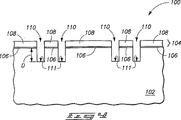
パターンニングされたマスク104が基板上に形成される。示されるパターンニングされたマスクは、二酸化シリコンからなる、実質的にからなる、あるいはのみからなる第一層106;と窒化シリコンからなる、実質的にからなる、あるいはのみからなる第二層108、を含む。マスク104上に光石版印刷のパターンニングされたフォトレジスト(図示しない)を用意し、フォトレジストからマスク104の材料へパターンを転写し、そして後にフォトレジストを除去することによってマスク104が示されるパターンへ形成がされる。
A
パターンニングされたマスク104はそこを通って拡がる開口部110を有し、そのような開口部で、凹状アクセスデバイス溝のための位置を規定する。開口部110の位置は後続の考察において第一位置とされる。
The patterned
基板102内部に拡張する凹状アクセスデバイス溝を形成するためにマスク104によって規定される第一位置を通して基板102がエッチングされる。特定の形態において、このような溝は基板102の単結晶シリコンに拡張する。溝は111の底面そして基板102の最上位表面から底面までの“D”の深さを有するように示されている。このような深さは、例えば、およそ100Åからおよそ2000Åまで可能である。
The
本発明の例示的な形態において、基板102は図3と4の処理段階においてp−ウェルと/またはn−ウェルのインプラントを中に有する単結晶シリコンを含むことができる。層106は単結晶シリコンの最上位表面を酸化することで形成することができ、層106は二酸化シリコンから実質的になりあるいはのみからなり、そしておよそ50Åからおよそ100Åの厚さを有する。窒化物キャップ108はおよそ200Åからおよそ500Åの厚さを含むことができ、そして、典型的におよそ300Åからおよそ500Åの厚さを含む。
In an exemplary form of the invention, the
幾つかの形態において(示されない)開口部110の微細寸法は2ステップ処理により縮めることができる。まず、示される開口部110を形成するためにマスキング層104がエッチングされる。後に、開口部110の側壁に沿って拡がりかつ開口部の内部に窒化シリコン層を用意し、そして後にスペーサーを形成するためこのような層に異方性エッチングを受けさせることで窒化物スペーサーが開口部110の側壁に沿って形成される。。このようなスペーサーの形成後に開口部が基板102内部に拡張させることができ、そのために、開口部は光石版印刷の処理で最初に形成された寸法よりもより小さい微細寸法を有する。
In some configurations, the fine dimensions of the opening 110 (not shown) can be reduced by a two-step process. First, the
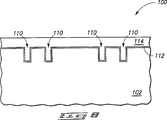
次に図5と6を参照し、マスク104(図3と4)が除去され、そして層112が基板102上と溝110内部に形成される。層112は、例えば、二酸化シリコンからなる、実質的にからなる、あるいはのみからなるように構成できる。このような形態において、層112は単結晶シリコン102の露出された上位表面を熱酸化で形成させることができる。
5 and 6, the mask 104 (FIGS. 3 and 4) is removed and a
次に図7と8を参照し、窒化シリコンからなる、実質的にからなる、あるいはのみからなる層114は層112上に形成される。ここに用意される層112と114の合成物は例示的な合成物として理解するこができ、そしてこれらの層はどんなふさわしい合成物を含むこともできることが理解するこができる。層112と114は共に溝110を満たすために用意された第一の絶縁性の材料とすることができる。絶縁性の材料114の下の溝の位置を示すために溝110は図7にて破線で示される。
Referring now to FIGS. 7 and 8, a
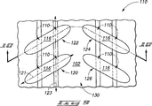
次に図9と10を参照して、光石版印刷のパンターンニングされたフォトレジスト116が層114上に用意される。フォトレジストは層112と114を含む第一絶縁材料へ転写されるパターンを規定する。その後、このようなパターンがふさわしいエッチングで層112と114に転写され、パターン層112と114がマスクへ転写される。マスクは複数のアクセスデバイス領域120、122、124と126を規定する。アクセスデバイス領域は分離領域130に囲まれる島状部である。アクセスデバイス領域120、122、124と126は分離領域130内部に溝の残りの部分を有し、最初に形成される凹まされたアクセスデバイス溝110の部分(つまり、図7と8の溝)のみを含む。
Next, with reference to FIGS. 9 and 10, a photolithographic
示されるアクセスデバイス領域120、122、124と126は図9において実質的に楕円である。実質的に楕円のアクセスデバイス領域は領域120内の軸121として示される例示的な主要縦楕円軸を持つ主要縦楕円軸を有する。溝110は図9内の軸123として図示される例示的な長手軸を持つそれらの長さに沿って拡張する主要長手軸を含むように考察できることが注意されたい。図9に図示される応用において、主要縦楕円軸121は軸123とは相互的に斜角をなし、そして従って主要縦軸123とは実質的に直交しない。しかしながら、本発明はまた、アクセスデバイス領域の主要縦楕円軸は実質的に凹まされたアクセスデバイス溝の主要長手軸へ直交するような形態も含むことが理解できる(例えば、この後に述べる図31と32に関連する形態など)。
The
次に図11と12を参照し、隔離領域の基板130がエッチングによって凹まされる。エッチングは凹状アクセスデバイス領域120、122、124と126間の溝110部分を除去する。
Next, referring to FIGS. 11 and 12, the
エッチング後、分離領域130の凹まされた基板は基板102の最上位表面の下の“E”の深さにある。特定の形態において、基板は凹状アクセスデバイス溝110の最下位レベルの下のレベルまで凹ませることができ、そのような深さ“E”は図4の深さ“D”より少なくともおよそ2倍大きい。深さ“E”は浅い溝分離領域の深さに対応でき、そして特定の形態においておよそ500Åからおよそ3500Åまで可能である。
After etching, the recessed substrate in
図12の2つの溝110はお互いに隣接するとみなせることができ、そして分離領域130はそのような隣接する溝間に形成されることがみなせることができる。例として、1つの隣接する溝は131でラベリングされた溝、そして他は133でラベリングされた溝であり、そしてそのような溝は分離領域130内でのそれらの間に形成された深い溝の向かい合い側にあるとみなせることができる。示される本発明の処理において、隣接する凹まされたアクセスデバイス溝131と133はそれらの間の深い溝の形成前に形成される。
The two
次に図13と14を参照し、フォトレジスト116(図11と12)が除去され、そして後に絶縁材料136が分離領域130のエッチングされた基板上に形成され、と同様にアクセスデバイス領域120、122,124と126の層114上に形成される。アクセスデバイス領域120、122,124と126がそのような領域の位置を指すために図13にて破線で示され、しかし、図13の処理段階においてこれらの領域は絶縁材料136の下にあることが注意されたい。
Referring now to FIGS. 13 and 14, the photoresist 116 (FIGS. 11 and 12) is removed and an insulating
材料136はどんなふさわしい合成物または合成物の組み合わせでも含むことができる。特定の形態において、材料136は浅い溝スタックと呼ばれるものに対応でき、そして従って基板102に沿った二酸化シリコンの薄い層、二酸化シリコン上の薄い窒化シリコンライナー、そしてライナー内部を満たす厚い二酸化シリコンを含むことができる。言い換えれば、絶縁材料136は元来薄い窒化シリコンライナーと薄い二酸化シリコンライナーによって基板102から分離される材料のバルク二酸化シリコンを持つ二酸化シリコンを含むことができる。材料136のバルク絶縁合成物は、幾つかの形態において、塗布誘電体であることができる。
図14において、誘電体で満たされた深い領域130は凹状アクセスデバイス溝131と133間に用意されるトレンチ分離領域を含むようにみなせることができる。
In FIG. 14, the
次に図15と16を参照し、層114上から材料を除去し、そして材料136と層114を横切って拡がる平坦化された上位表面137を形成するために材料136が平坦化を受けさせられる(例えば、化学機械平坦化など)。図15と16の平坦化は分離領域130の凹まされた基板上の絶縁材料136を残しながら層114上から絶縁材料136を除去するとみなせることができる。
Referring now to FIGS. 15 and 16,
次に図17と18を参照して、絶縁材料136を残しながら層112と114が基板102上から除去される。幾つかの形態において、層112と114は共に第一絶縁材料を含むように考えることができそして材料136に対応する第二絶縁材料が少なくとも大部分残されながらそのような第一絶縁材料が少なくとも大部分除去されると考えることができる。示される形態において、層112と114に対応する第一絶縁材料の全体が除去され、しかし本発明はそのような材料の全体よりも少ない量が除去される他の形態を含むことができると理解されたい。例として、材料112は二酸化シリコンを含めば、後続処理におけるゲート酸化に対応するように材料112が残されるようにできる。しかしながら、材料112は二酸化シリコンを含むか否かにもかかわらず材料112が除去されれば、このように実際のゲート誘電体材料の形成前に基盤102の表面が浄化されることを可能とする点で有利である。従って、層122と114の材料は典型的に犠牲材料に対応する。
Referring now to FIGS. 17 and 18,
例えば、p−ウェルまたはn−ウェルのようなドーパントウェルの形成要求があれば、ドーパントが図17と18の処理段階において基板102内部に用意されることができる。
For example, if there is a requirement to form a dopant well such as a p-well or an n-well, the dopant can be provided within the
次に図19と20を参照し、ゲート誘電体材料140が凹状アクセスデバイス溝110内部に形成され、そして後に導電性のゲート材料142がゲート誘電体材料上にそして溝を満たすために溝内部に形成される。示される本発明の形態において、伝導性のゲート材料142は第一層144と第二層146を含む。層144と146はインタフェース147において結びつく。層144は、例えば、導電性のドープされたシリコンからなる、実質的にはからなる、あるいはのみからなる。そして層146は、例えば、1つまたはそれ以上の金属を含んだ合成物からなる、実質的にはからなる、またはのみからなるように構成することができる。金属含有の合成物は純金属そして/または金属含有の混合物であることができる。特定の形態において、層146は図20にて降順でタングステン/タングステンケイ化物/窒化チタンのスタックを含むように構成できる。
Referring now to FIGS. 19 and 20, a
示されるゲート材料142は溝110を満たすのみにならず、しかしまたそのような溝の外部まで拡がる。さらに、層146の金属含有の合成物と層144の導電性のドープされたシリコン間のインタフェース(つまり、インタフェース147)は溝の外にある。
The
絶縁キャップ150が導電性のゲート材料142上に形成される。キャップ150はどんなふさわしい合成物または合成物の組み合わせでも含むことができ、そして特定の形態において二酸化シリコンと窒化シリコンの内の1つまたは両方からなる、実質的にはからなる、あるいはのみからなるように構成する。
An
図19にてアクセスデバイス領域120、122、124と126が破線で示され、その領域は絶縁キャップ150の下にあることを指す。
In FIG. 19,
次に図21と22を参照し、材料140、144、146と150がアクセスデバイス領域120、122、124と126を横切って延びる導電性の線へパターンニングされる。より具体的に、材料140、144,146と150は複数の線160、162、164と166へパターンニングされ、各々の線は複数のアクセスデバイス領域を横切って延びそして異なるアクセスデバイス領域と関連するゲートをお互いに電気的に接続する。
Referring now to FIGS. 21 and 22, the
ソース/ドレイン領域170、172、174、176,178と180は基板102内部そして電気的に導電性のゲート材料144の近くに形成される。ソース/ドレイン領域がどんなふさわしいドーパント型へもドープされることができ、そしてどんなふさわしいドーパントでも含むことができる。ソース/ドレインは基板102内部にドーパントを妥当な深さまで打ち込むことによって形成されることができる。導電性のゲート材料とソース/ドレイン領域は共に基板102に支えられる複数のトランジスタデバイス180、182、184と186を形成する。そのようなトランジスタデバイスは凹状アクセス装置溝110内部に拡がるゲートを有する凹状アクセスデバイスに対応する。
Source /
各々のトランジスタデバイス180、182、184と186はソース/ドレイン領域の対をお互いに電気的に接続するゲートを含むものとして考えることができる。例として、トランジスタデバイス180はソース/ドレイン領域170と172をお互いに電気的に接続するゲートを含むものとして考えることができ、デバイス182はソース/ドレイン領域172と174とをお互いに電気的に接続するゲートを含むものとして考えることができ、デバイス184はソース/ドレイン領域176と178とをお互いに電気的に接続するゲートを含むものとして考えることができ、デバイス186はソース/ドレイン領域170と172とをお互いに電気的に接続するゲートを含むものとして考えることができる。
Each
トランジスタデバイスは幾つかの対となったソース/ドレイン領域をビット線の接点そして他を記憶装置ノードの接点(つまり、コンデンサー記憶装置ノード)へ接続することでダイナミックスアクセスメモリ(DRAM)アレイへ組み入れることができる。示される本発明の形態において、ソース/ドレイン領域170、174、176と180がそれぞれコンデンサー記憶デバイスノード190、192、194と196に接続される;そしてソース/ドレイン領域172と178がそれぞれビット線198と200に接続される。故に、示された構造はDRAMアレイへ組み入れることができる。
Transistor devices incorporate several pairs of source / drain regions into a dynamics access memory (DRAM) array by connecting bit line contacts and others to storage node contacts (ie, capacitor storage nodes). be able to. In the form of the invention shown, source /
次に図23と24を参照し、本発明の第二実施例の形態の予備処理段階における半導体構造300を図解する。本発明の第二実施例の形態に関連する図に関して、妥当な所において上記の本発明の第一実施例の形態の説明に使われた同様の番号付けが使われる。
Referring now to FIGS. 23 and 24, a
構造300は上述の図3と4に関連する基板102、層106と108のパターンニングされたマスク104、そして溝110を含み、そして故に上述の図3と4に関する構造に同一に対応する。
次に図25と26を参照し、ゲート誘電体材料302が形成され溝110の底を線引き、そしてその後ゲート材料304が溝内部にそして誘電体材料302上に形成される。
Referring now to FIGS. 25 and 26, a
誘電体材料302は、例えば、二酸化シリコンからなる、実質的にはからなる、あるいはのみからなるように構成することができる。そのような形態において、溝110内部に基板102から露出したシリコンを酸化することによって材料302が堆積または形成されるようにすることができる。要求されれば、誘電体材料302が2ステップで形成されることができ、1つのステップは溝110内部に第一の二酸化シリコンを最初に形成し、そして他のステップは溝110内部から第一誘電体材料を取り除きそして他の誘電体材料を溝内部に形成し最初に用意されたものより良質の二酸化シリコン誘電体ができる。
The
ゲート材料304はシリコンからなる、実質的にはからなる、あるいはのみからなるように構成することができる。シリコンは堆積された導電性のドープ、または非導電性のドープ形で堆積されそしてその後の処理段階で妥当な打ち込みでドープされるようにできる。
The
図26の構造はゲート材料304を横切りそして絶縁材料108を横切って拡がる平坦化された上位表面305を含むように示される。これは溝を満たすと同時に材料108をかぶせるゲート材料304を最初に用意し、そして後に材料304に平坦化を受けさせ(例えば、化学機械平坦化など)、材料108上から材料304を除去して平坦化された上位表面305を形成する。
The structure of FIG. 26 is shown to include a planarized
要求されれば、溝110内部のゲート材料304の形成前に強化打ち込みそして/または閾値電圧打ち込みが基板102内部に用意されることができる。
If desired, a reinforced implant and / or a threshold voltage implant can be provided within the
ゲート材料304が層108の最上位表面と同一の広がりを持つ平坦化された表面を有するように示されているが、ゲート材料はまた層108の最上位表面の高度レベルより下
に凹まされた表面を有することができることが理解されたい。幾つかの形態において、シリコンを含んだ材料304が層108の最上位表面より下に凹まされることが好まれる。
Although the
次に図27と28を参照し、層108上に酸化物310そして層304上に酸化物312を形成するために、材料304の最上位表面と層108に酸化を受ける。本発明の特定の形態において、層108は窒化シリコンからなる、実質的にはからなる、あるいはのみからなるように構成し、そして従って酸化物310は窒化酸化シリコンからなる、実質的にはからなる、あるいはのみからなるように構成し、そして層304はシリコンからなる、実質的にはからなる、あるいはのみからなるように構成し、そして従って酸化物312は二酸化シリコンからなる、実質的にはからなる、あるいはのみからなるように構成する。酸化物310と312はおよそ30Åの厚さからおよそ60Åの厚さになるように形成される。
Referring now to FIGS. 27 and 28, the top surface of
次に図29と30を参照し、絶縁材料314が酸化物310と312上に用意される。層314は、例えば、窒化シリコンからなる、実質的にはからなる、あるいはのみからなるように構成することができ、そしておよそ300Åからおよそ500Åまでの厚さで堆積させられることができる。本発明の幾つかの形態において、合成物310、312と314が共に第一パンターンニングされたマスク104とゲート材料304上に用意される絶縁材料316を形成するとみなせることできる。
Next, referring to FIGS. 29 and 30, an insulating
溝の位置を指すために溝110は図29において破線で示される。
To indicate the position of the groove, the
次に図31と32を参照し、材料316が複数のアクセスデバイス領域320、324、326、328、330、332、334と336を規定するマスクへパタンーンニングされる;そしてアクセスデバイス領域を囲む分離領域340を規定する。材料316のパターンニングは材料316上に光石版印刷のパターンニングされたフォトレジストマスク(示されない)を用意し、フォトレジストから材料316にパターンを転写し、そして後にフォトレジストマスクを除去することで成し遂げることができる。
31 and 32,
材料316がパターンニングされた後、基板102が分離領域340内部でエッチングされ、そのような分離領域の基板を凹ませる。分離領域の凹まされた基板は溝110の最下位の高さレベルの下の高さレベルにあり、そして幾つかの形態において少なくとも溝110の高さレベルより2倍深い。
After the
分離領域340内部のエッチングはアクセスデバイス領域320、324、326、328、330、332、334と336内部のゲート材料を残しながら分離領域内部からゲート材料304を除去する。分離領域340内部のエッチングは、例えば、反応性イオンエッチングによって成し遂げることができる。
Etching within the
酸化物342と窒化ライナー344がエッチングされた分離領域340内部に用意され、そしてまた示される形態において材料314上に拡がる。酸化物312は、例えば、基板102を沿う二酸化シリコンからなる、実質的にはからなる、あるいはのみからなるように構成することができ、そして窒化物344は、例えば、窒化シリコンからなる、実質的にはからなる、あるいはのみからなるように構成することができる。酸化物は構造300の露出された材料の酸化によって形成されることができ、そして従って材料108と314を沿うより基板102を沿った他の合成物を含むことができ、またはその代わりに堆積によって構成されることができる。このように反応性イオンエッチング中に出現しうるプラズマダメージを修復することができる点から酸化が望ましく、そしてまたゲート多結晶シリコンと基板102のバルクシリコン間に低い漏れを提供するために界面表面におけるゲート誘電体への侵食ができる。酸化物はおよそ30Åからおよそ80Åまでの厚さで形成されることが望ましい。窒化物ライナー344は酸化物層342上に堆積されることができ、そして最終的に後続の塗布ガラス堆積プロセスのための保護層として機能することができる。
An
図9のアクセスデバイス領域に類似して図31のアクセスデバイス領域が楕円として示されていることに注意されたい。しかしながら、図9のアクセスデバイス領域と違って、図31のアクセスデバイス領域は主要元来縦楕円軸を有し、凹まされたアクセスデバイス溝110の主要長手軸に実質的に直交する。
Note that the access device region of FIG. 31 is shown as an ellipse, similar to the access device region of FIG. However, unlike the access device regions of Fig. 9, the access device regions of Fig. 31 has a main originally vertical ellipse axis, substantially perpendicular to the main longitudinal axis of the
次に図33と34を参照し、誘電体材料350がトレンチ分離領域340を満たすために用意される。誘電体材料350は塗布グラスであることできる。誘電体材料350が絶縁材料316を覆うために最初に形成されることができ、と同時にトレンチ分離領域340を満たし、そして後に絶縁材料316を除去してそして誘電体材料350と層314上が拡がる平坦化された表面351を形成するために平坦化(例えば、化学機械研磨など)が使用されることができる。幾つかの形態において、絶縁材料316(材料314、310と312を含む)は第一絶縁材料として考えることができ、そして絶縁材料350は第二絶縁材料として考えることができる。
Referring now to FIGS. 33 and 34, a
次に図35と36を参照し、層314(図34)が除去される。これはウェット酸化物エッチングで材料314の窒化物より下の塗布ガラスを軽く凹ませ、続いて材料314除去するためにウェット窒化物を取り除くなどで成し遂げることができる。ウェット窒化物の取り除きは酸化物材料310と312にて選択的に停止することができる。
Referring now to FIGS. 35 and 36, layer 314 (FIG. 34) is removed. This can be accomplished, for example, by lightly denting the coated glass below the nitride of
次に図37と38を参照し、複数の線370、372、374と376がアクセスデバイス領域320、324、326、328、330、332、334と336を横切って延びるように形成される。線は導電性の材料380と絶縁キャップ382を含む。導電性の材料380は、例えば、窒化チタン/タングステンケイ化物/タングステンのスタック(図20にて降順)を含むことができ、そしてキャップ382は窒化シリコンからなる、実質的にはからなる、あるいはのみからなることができる。
Referring now to FIGS. 37 and 38, a plurality of
線は層380と382のふさわしい材料を構造300の最上位表面を全体的に横切って最初に堆積させ、そして後に層380と382上に光石版印刷のパンターンニングされたフォトレジストを形成し、フォトレジストからパターンを下にある層380と382上に転写し、そして後にフォトレジストを除去することで材料のパターンニングをすることによって形成することができる。
The lines first deposit the appropriate material of
図37と38の構造は図21と22の構造と類似してダイナミックスアクセスメモリ(DRAM)アレイへ組み入れることができる。特に、妥当な伝導性のドープされた拡散領域が導電性のゲート材料144によって構成されるトランジスタゲートの近くに形成されることができ、そしてコンデンサー構造とビットライン構造が電気的にソース/ドレイン領域に結合されることができる。
The structure of FIGS. 37 and 38 can be incorporated into a dynamics access memory (DRAM) array similar to the structure of FIGS. In particular, a reasonable conductive doped diffusion region can be formed near the transistor gate constituted by the
図39と40は図37と38に関連する形態の別の形態について図示する。特に、線370、372、374と376の形成の前に構造300に平坦化を受けさせることができる。そのような平坦化は層108を除去し(図35と36)、そして示される平坦化された表面390を形成する。平坦化された表面390が材料106上に示されるが材料106を通して平坦化がまた拡がることが理解されたい。材料106を通して平坦化がまた拡がれば、線の形成前に他の誘電体の材料が基板102上に材料106のかわりに形成されることができる。図40の構造が図39の構造に関連する上述の類似方法でメモリアレイに取り込むことができる。
39 and 40 illustrate another form associated with FIGS. 37 and 38. FIG. In particular, the
本発明の好まれる実施例が下記の関連する図面で説明される。
10 半導体構造
12 基板
14 トランジスタデバイス
16 ゲート
18 誘電体材料
20 ソース/ドレイン領域
22 チャネル領域
24 側壁スペーサー
30 構造
32 半導体基板
34 トランジスタ
36 ゲート
38 誘電体材料
40 ソース/ドレイン領域
42 チャネル領域
100 半導体構造
102 基板
104 マスク
106 第一層
108 第二層
110 開口部
111 底面
112 層
114 層
116 フォトレジスト
120、122、124、126 アクセスデバイス領域
121 主要縦楕円軸
123 主要長手軸
130 分離領域
131、133 アクセスデバイス溝
136 絶縁材料
140 ゲート誘電体材料
142 導電性のゲート材料
144 第一層
146 第二層
147 インタフェース
150 キャップ
160、162、164、166 線
170、172、174、176,178、180 ソース/ドレイン領域
180、182、184、186 トランジスタデバイス
190、192、194、196 コンデンサー記憶デバイスノード
198、200ビット線
300 半導体構造
302 ゲート誘電体材料
304 ゲート材料
305 上位表面
310、312 酸化物
314 絶縁材料
320、324、326、328、330、332、334、336 アクセスデバイス領域
340 分離領域
316 材料
342 酸化物
344 窒化ライナー
350 誘電体材料
370、372、374、376 線
380 導電性の材料
382 絶縁キャップ
390 表面
DESCRIPTION OF
30
100
112 layers
114 layers
130
140 Gate
160, 162, 164, 166
300
310, 312
350
Claims (7)
前記基板内部に凹状アクセスデバイス溝を形成し、前記凹状アクセスデバイス溝の一対は他の凹状アクセスデバイス溝の一対と隣接し、
電気的に導電性のゲート材料を前記凹状アクセスデバイス溝内部に形成し、
ソース/ドレイン領域を前記導電性のゲート材料の隣に形成し、前記導電性のゲート材料と前記ソース/ドレイン領域は共に凹状アクセスデバイスに対応するトランジスタデバイスを形成し、
前記凹状アクセスデバイス溝の一対と隣接する前記他の凹状アクセスデバイス溝の一対との間に分離領域溝を形成し、
トレンチ分離領域を形成するために前記分離領域溝を絶縁材料で満たす
ことを特徴とする半導体構造に関連する凹状アクセスデバイスの形成方法。Prepare a semiconductor substrate,
Forming a concave access device groove inside the substrate, wherein the pair of concave access device grooves is adjacent to another pair of concave access device grooves;
Forming an electrically conductive gate material within the recessed access device groove;
A source / drain region is formed next to the conductive gate material, and the conductive gate material and the source / drain region together form a transistor device corresponding to a concave access device ;
The isolation region trench is formed between the pair of the other recessed access device trenches and the adjacent pair of the recessed access device trenches,
A method of forming a concave access device associated with a semiconductor structure, wherein the isolation region trench is filled with an insulating material to form a trench isolation region.
前記基板内部に凹状アクセスデバイス溝を形成し、
前記凹状アクセスデバイス溝を第一絶縁材料で満たし、
複数のアクセスデバイス領域を規定するマスクに前記第一絶縁材料をパターンニングし、前記アクセスデバイス領域が孤立され、分離領域によって囲まれ、前記アクセスデバイス領域は前記凹状アクセスデバイス溝の部分のみを含み、
前記分離領域を前記基板に凹ますために前記分離領域の基板内部をエッチングし、
前記エッチングした基板を第二絶縁材料で被覆し、前記第二絶縁材料で前記分離領域を被覆し、
前記第二絶縁材料を残しながら前記第一絶縁材料を除去し、
前記第一絶縁材料を除去した後、前記アクセスデバイス領域に含まれる前記凹状アクセスデバイス溝の部分内部にゲート材料を形成する
ことを特徴とする半導体構造に関連する凹状アクセスデバイスの形成方法。Prepare a semiconductor substrate,
Forming a concave access device groove in the substrate;
Filling the concave access device groove with a first insulating material;
Patterning the first insulating material in a mask defining a plurality of access device regions, wherein the access device region is isolated and surrounded by an isolation region, the access device region including only a portion of the concave access device groove;
Etching the inside of the substrate in the separation region to dent the separation region into the substrate;
Coating the etched substrate with a second insulating material, covering the isolation region with the second insulating material;
Removing the first insulating material while leaving the second insulating material;
The first after the insulating material is removed, the method of forming the concave access devices associated with semiconductor structures and forming the recessed access device trenches portion inside the gate material included in the access device region.
前記第一絶縁材料上と前記分離領域の前記エッチングした基板上に前記第二絶縁材料を形成し、
前記分離領域の前記エッチングした基板上の前記第二絶縁材料を残しながら前記第一絶縁材料上から前記第二絶縁材料を除去するために前記第二絶縁材料を平坦化することによって成し遂げられる
ことを特徴とする請求項2記載の形成方法。The coating of the etched substrate with the second insulating material is:
Forming the second insulating material on the first insulating material and on the etched substrate in the isolation region;
Accomplished by planarizing the second insulating material to remove the second insulating material from the first insulating material while leaving the second insulating material on the etched substrate in the isolation region. The forming method according to claim 2, wherein:
ゲート材料は電気的に相互的にソース/ドレイン対を相互接続するゲートを含み、
少なくとも幾つかの対となったソース/ドレイン領域はビット線接続点と格納装置ノード接続点を含み、そしてDRAM装置に組み入れられる
ことをさらに含むことを特徴とする請求項2記載の形成方法。Forming a source / drain region next to the gate material of the concave access device region;
The gate material includes a gate electrically interconnecting the source / drain pairs;
The method of claim 2, further comprising: incorporating at least some of the paired source / drain regions including a bit line connection point and a storage device node connection point into a DRAM device.
前記基板上に第一のパターンニングされたマスクを形成し、前記第一のパターンニングされたマスクは前記基板内部に拡張する開口部を有し、凹状アクセスデバイス溝の第一位置を規定し、
前記基板内部に拡張する凹状アクセスデバイス溝を形成するために前記第一位置を通じて前記基板をエッチングし、
前記凹状アクセスデバイス溝をゲート材料で満たし、
前記第一のパターンニングされたマスク上と前記ゲート材料上に第一絶縁材料を形成し、
複数のアクセスデバイス領域を規定するマスクに前記第一絶縁材料をパターンニングし、前記アクセスデバイス領域が孤立され、分離領域によって囲まれ、前記アクセスデバイス領域は前記凹状アクセスデバイス溝の部分のみを含み、
前記分離領域を前記基板に凹ますために基板内部をエッチングし、前記エッチングはまた前記アクセスデバイス領域内部の前記ゲート材料を残しながら前記アクセスデバイス領域間から前記ゲート材料を除去し、
前記エッチングした基板を第二絶縁材料で被せて前記第二絶縁材料で前記分離領域を被覆し、
前記第一絶縁材料を除去し、
前記第一絶縁材料を除去した後、複数の導電性の線を形成し、各々の導電性の線は複数のアクセスデバイス領域を横切って拡がりそして前記複数のアクセスデバイス領域のゲート材料をお互いに電気的に相互接続する
ことを特徴とする半導体構造に関連する凹状アクセスデバイスの形成方法。Prepare a semiconductor substrate,
Forming a first patterned mask on the substrate, the first patterned mask having an opening extending into the substrate and defining a first position of the concave access device groove;
Etching the substrate through the first location to form a concave access device groove extending into the substrate;
Filling the concave access device groove with a gate material;
Forming a first insulating material on the first patterned mask and on the gate material;
Patterning the first insulating material in a mask defining a plurality of access device regions, wherein the access device region is isolated and surrounded by an isolation region, the access device region including only a portion of the concave access device groove;
Etching the interior of the substrate to recess the isolation region into the substrate, the etching also removing the gate material from between the access device regions while leaving the gate material within the access device region;
Covering the etched region with a second insulating material and covering the isolation region with the second insulating material;
Removing the first insulating material;
After removing the first insulating material, a plurality of conductive lines are formed, each conductive line extending across the plurality of access device regions and electrically connecting the gate materials of the plurality of access device regions to each other. A method of forming a concave access device associated with a semiconductor structure, characterized in that:
前記第一のパターンニングされたマスクを被覆しそして前記溝内部に前記ゲート材料を形成し、
前記凹状アクセスデバイス溝内部の前記ゲート材料を残しながら前記第一のパターンニングされたマスク上から前記ゲート材料を除去するために前記ゲート材料を平坦化することを含む
ことを特徴とする請求項5記載の形成方法。Filling the concave access device groove with a gate material covers the first patterned mask and forms the gate material within the groove;
The planarization of the gate material to remove the gate material from the first patterned mask while leaving the gate material inside the concave access device trench. The forming method as described.
前記基板内部に凹状アクセスデバイス溝を形成し、前記凹状アクセスデバイス溝の一対は他の凹状アクセスデバイス溝の一対と隣接し、
前記凹状アクセスデバイス溝の一対と隣接する前記他の凹状アクセスデバイス溝の一対との間に分離領域溝を形成し、
トレンチ分離領域を形成するために前記分離領域溝を絶縁材料で満たし、
電気的に導電性のゲート材料を前記凹状アクセスデバイス溝内部に形成し、
ソース/ドレイン領域を前記導電性のゲート材料の隣に形成し、前記導電性のゲート材料と前記ソース/ドレイン領域は共に凹状アクセスデバイスに対応するトランジスタデバイスを形成する
ことを特徴とする半導体構造に関連する凹状アクセスデバイスの形成方法。 Prepare a semiconductor substrate,
Forming a concave access device groove inside the substrate, wherein the pair of concave access device grooves is adjacent to another pair of concave access device grooves;
Forming a separation region groove between a pair of the concave access device grooves and a pair of the other concave access device grooves adjacent thereto;
Filling the isolation region trench with an insulating material to form a trench isolation region;
Forming an electrically conductive gate material within the recessed access device groove;
A source / drain region is formed next to the conductive gate material, and the conductive gate material and the source / drain region together form a transistor device corresponding to a concave access device.
A method of forming a concave access device associated with a semiconductor structure .
Applications Claiming Priority (3)
| Application Number | Priority Date | Filing Date | Title |
|---|---|---|---|
| US11/090,529 US7384849B2 (en) | 2005-03-25 | 2005-03-25 | Methods of forming recessed access devices associated with semiconductor constructions |
| US11/090,529 | 2005-03-25 | ||
| PCT/US2006/008295 WO2006104654A1 (en) | 2005-03-25 | 2006-03-08 | Methods of forming recessed access devices |
Publications (2)
| Publication Number | Publication Date |
|---|---|
| JP2008535217A JP2008535217A (en) | 2008-08-28 |
| JP4962874B2 true JP4962874B2 (en) | 2012-06-27 |
Family
ID=36676528
Family Applications (1)
| Application Number | Title | Priority Date | Filing Date |
|---|---|---|---|
| JP2008503014A Active JP4962874B2 (en) | 2005-03-25 | 2006-03-08 | Method for forming concave access device |
Country Status (8)
| Country | Link |
|---|---|
| US (3) | US7384849B2 (en) |
| EP (2) | EP1880421B1 (en) |
| JP (1) | JP4962874B2 (en) |
| KR (1) | KR100895568B1 (en) |
| CN (1) | CN100536142C (en) |
| AT (1) | ATE533183T1 (en) |
| TW (1) | TWI314769B (en) |
| WO (1) | WO2006104654A1 (en) |
Families Citing this family (76)
| Publication number | Priority date | Publication date | Assignee | Title |
|---|---|---|---|---|
| US5977579A (en) | 1998-12-03 | 1999-11-02 | Micron Technology, Inc. | Trench dram cell with vertical device and buried word lines |
| US7071043B2 (en) | 2002-08-15 | 2006-07-04 | Micron Technology, Inc. | Methods of forming a field effect transistor having source/drain material over insulative material |
| US6844591B1 (en) * | 2003-09-17 | 2005-01-18 | Micron Technology, Inc. | Method of forming DRAM access transistors |
| US7262089B2 (en) * | 2004-03-11 | 2007-08-28 | Micron Technology, Inc. | Methods of forming semiconductor structures |
| KR100538101B1 (en) * | 2004-07-07 | 2005-12-21 | 삼성전자주식회사 | Semiconductor device and method of manufacturing for the same |
| US7518182B2 (en) * | 2004-07-20 | 2009-04-14 | Micron Technology, Inc. | DRAM layout with vertical FETs and method of formation |
| US7547945B2 (en) | 2004-09-01 | 2009-06-16 | Micron Technology, Inc. | Transistor devices, transistor structures and semiconductor constructions |
| US7244659B2 (en) * | 2005-03-10 | 2007-07-17 | Micron Technology, Inc. | Integrated circuits and methods of forming a field effect transistor |
| US7384849B2 (en) | 2005-03-25 | 2008-06-10 | Micron Technology, Inc. | Methods of forming recessed access devices associated with semiconductor constructions |
| US7282401B2 (en) | 2005-07-08 | 2007-10-16 | Micron Technology, Inc. | Method and apparatus for a self-aligned recessed access device (RAD) transistor gate |
| US7867851B2 (en) | 2005-08-30 | 2011-01-11 | Micron Technology, Inc. | Methods of forming field effect transistors on substrates |
| US7867845B2 (en) * | 2005-09-01 | 2011-01-11 | Micron Technology, Inc. | Transistor gate forming methods and transistor structures |
| US7700441B2 (en) | 2006-02-02 | 2010-04-20 | Micron Technology, Inc. | Methods of forming field effect transistors, methods of forming field effect transistor gates, methods of forming integrated circuitry comprising a transistor gate array and circuitry peripheral to the gate array, and methods of forming integrated circuitry comprising a transistor gate array including first gates and second grounded isolation gates |
| US20070262395A1 (en) | 2006-05-11 | 2007-11-15 | Gibbons Jasper S | Memory cell access devices and methods of making the same |
| US8008144B2 (en) | 2006-05-11 | 2011-08-30 | Micron Technology, Inc. | Dual work function recessed access device and methods of forming |
| US8860174B2 (en) * | 2006-05-11 | 2014-10-14 | Micron Technology, Inc. | Recessed antifuse structures and methods of making the same |
| KR100766233B1 (en) * | 2006-05-15 | 2007-10-10 | 주식회사 하이닉스반도체 | Flash memory device and method for fabricating the same |
| US8852851B2 (en) | 2006-07-10 | 2014-10-07 | Micron Technology, Inc. | Pitch reduction technology using alternating spacer depositions during the formation of a semiconductor device and systems including same |
| US7602001B2 (en) | 2006-07-17 | 2009-10-13 | Micron Technology, Inc. | Capacitorless one transistor DRAM cell, integrated circuitry comprising an array of capacitorless one transistor DRAM cells, and method of forming lines of capacitorless one transistor DRAM cells |
| DE102006035667B4 (en) * | 2006-07-31 | 2010-10-21 | Advanced Micro Devices, Inc., Sunnyvale | A method of improving lithography properties during gate fabrication in semiconductors having a pronounced surface topography |
| US7772632B2 (en) | 2006-08-21 | 2010-08-10 | Micron Technology, Inc. | Memory arrays and methods of fabricating memory arrays |
| US7589995B2 (en) | 2006-09-07 | 2009-09-15 | Micron Technology, Inc. | One-transistor memory cell with bias gate |
| KR100763337B1 (en) * | 2006-10-02 | 2007-10-04 | 삼성전자주식회사 | Semiconductor device having buried gate line and method of fabricating the same |
| KR100771552B1 (en) * | 2006-10-31 | 2007-10-31 | 주식회사 하이닉스반도체 | Mos transistor depressing short channel effect and method of fabricating the same |
| JP2008171863A (en) * | 2007-01-09 | 2008-07-24 | Elpida Memory Inc | Method of forming trench gate |
| JP2008171872A (en) * | 2007-01-09 | 2008-07-24 | Elpida Memory Inc | Semiconductor device and manufacturing method thereof |
| US7768047B2 (en) * | 2007-05-10 | 2010-08-03 | Micron Technology, Inc. | Imager element, device and system with recessed transfer gate |
| US7923373B2 (en) | 2007-06-04 | 2011-04-12 | Micron Technology, Inc. | Pitch multiplication using self-assembling materials |
| KR100825815B1 (en) * | 2007-06-07 | 2008-04-28 | 삼성전자주식회사 | Semiconductor device including active pattern with channel recess, and method of fabricating the same |
| JP2009141260A (en) * | 2007-12-10 | 2009-06-25 | Elpida Memory Inc | Semiconductor device, and manufacturing method thereof |
| US7875919B2 (en) * | 2008-03-31 | 2011-01-25 | International Business Machines Corporation | Shallow trench capacitor compatible with high-K / metal gate |
| US7989307B2 (en) | 2008-05-05 | 2011-08-02 | Micron Technology, Inc. | Methods of forming isolated active areas, trenches, and conductive lines in semiconductor structures and semiconductor structures including the same |
| US7687862B2 (en) * | 2008-05-13 | 2010-03-30 | Infineon Technologies Ag | Semiconductor devices with active regions of different heights |
| US10151981B2 (en) | 2008-05-22 | 2018-12-11 | Micron Technology, Inc. | Methods of forming structures supported by semiconductor substrates |
| US7824983B2 (en) * | 2008-06-02 | 2010-11-02 | Micron Technology, Inc. | Methods of providing electrical isolation in semiconductor structures |
| US7824986B2 (en) | 2008-11-05 | 2010-11-02 | Micron Technology, Inc. | Methods of forming a plurality of transistor gates, and methods of forming a plurality of transistor gates having at least two different work functions |
| US8796155B2 (en) | 2008-12-04 | 2014-08-05 | Micron Technology, Inc. | Methods of fabricating substrates |
| US8247302B2 (en) | 2008-12-04 | 2012-08-21 | Micron Technology, Inc. | Methods of fabricating substrates |
| KR101561061B1 (en) * | 2009-04-10 | 2015-10-16 | 삼성전자주식회사 | Semiconductor device having a protrusion typed isolation layer |
| KR101159900B1 (en) * | 2009-04-22 | 2012-06-25 | 에스케이하이닉스 주식회사 | Semiconductor device and method of fabricating the same |
| US9330934B2 (en) | 2009-05-18 | 2016-05-03 | Micron Technology, Inc. | Methods of forming patterns on substrates |
| US8039340B2 (en) | 2010-03-09 | 2011-10-18 | Micron Technology, Inc. | Methods of forming an array of memory cells, methods of forming a plurality of field effect transistors, methods of forming source/drain regions and isolation trenches, and methods of forming a series of spaced trenches into a substrate |
| EP2477216A1 (en) | 2011-01-13 | 2012-07-18 | Soitec | Hybrid bulk/SOI device with a buried doped layer and manufacturing method thereof |
| US8575032B2 (en) | 2011-05-05 | 2013-11-05 | Micron Technology, Inc. | Methods of forming a pattern on a substrate |
| US9401363B2 (en) | 2011-08-23 | 2016-07-26 | Micron Technology, Inc. | Vertical transistor devices, memory arrays, and methods of forming vertical transistor devices |
| US9385132B2 (en) * | 2011-08-25 | 2016-07-05 | Micron Technology, Inc. | Arrays of recessed access devices, methods of forming recessed access gate constructions, and methods of forming isolation gate constructions in the fabrication of recessed access devices |
| US9177794B2 (en) | 2012-01-13 | 2015-11-03 | Micron Technology, Inc. | Methods of patterning substrates |
| US8648407B2 (en) * | 2012-01-14 | 2014-02-11 | Nanya Technology Corporation | Semiconductor device and method for fabricating thereof |
| US8703550B2 (en) * | 2012-06-18 | 2014-04-22 | International Business Machines Corporation | Dual shallow trench isolation liner for preventing electrical shorts |
| US8629048B1 (en) | 2012-07-06 | 2014-01-14 | Micron Technology, Inc. | Methods of forming a pattern on a substrate |
| US9768055B2 (en) * | 2012-08-21 | 2017-09-19 | Stmicroelectronics, Inc. | Isolation regions for SOI devices |
| US9005463B2 (en) | 2013-05-29 | 2015-04-14 | Micron Technology, Inc. | Methods of forming a substrate opening |
| JP6681828B2 (en) | 2014-05-22 | 2020-04-15 | Jxtgエネルギー株式会社 | Refrigerating machine oil and working fluid composition for refrigerator |
| US10096696B2 (en) * | 2014-06-03 | 2018-10-09 | Micron Technology, Inc. | Field effect transistors having a fin |
| TWI704647B (en) * | 2015-10-22 | 2020-09-11 | 聯華電子股份有限公司 | Integrated circuit and process thereof |
| US10199461B2 (en) * | 2015-10-27 | 2019-02-05 | Texas Instruments Incorporated | Isolation of circuit elements using front side deep trench etch |
| US10128251B2 (en) * | 2016-09-09 | 2018-11-13 | United Microelectronics Corp. | Semiconductor integrated circuit structure and method for forming the same |
| US10347635B2 (en) * | 2017-06-30 | 2019-07-09 | Micron Technology, Inc. | Apparatuses comprising memory cells, and apparatuses comprising memory arrays |
| US10431695B2 (en) | 2017-12-20 | 2019-10-01 | Micron Technology, Inc. | Transistors comprising at lease one of GaP, GaN, and GaAs |
| US10825816B2 (en) * | 2017-12-28 | 2020-11-03 | Micron Technology, Inc. | Recessed access devices and DRAM constructions |
| US10319586B1 (en) | 2018-01-02 | 2019-06-11 | Micron Technology, Inc. | Methods comprising an atomic layer deposition sequence |
| US10734527B2 (en) | 2018-02-06 | 2020-08-04 | Micron Technology, Inc. | Transistors comprising a pair of source/drain regions having a channel there-between |
| US10818665B2 (en) | 2018-08-24 | 2020-10-27 | Micron Technology, Inc. | Array of recessed access devices and an array of memory cells individually comprising a capacitor and a transistor |
| US11810901B2 (en) | 2021-06-10 | 2023-11-07 | Micron Technology, Inc. | Microelectronic devices, related memory devices and electronic systems, and methods of forming microelectronic devices |
| US11848309B2 (en) | 2021-06-10 | 2023-12-19 | Micron Technology, Inc. | Microelectronic devices, related electronic systems, and methods of forming microelectronic devices |
| US11785764B2 (en) | 2021-06-30 | 2023-10-10 | Micron Technology, Inc. | Methods of forming microelectronic devices |
| US11810838B2 (en) | 2021-06-30 | 2023-11-07 | Micron Technology, Inc. | Microelectronic devices, and related electronic systems and methods of forming microelectronic devices |
| US11930634B2 (en) | 2021-06-30 | 2024-03-12 | Micron Technology, Inc. | Methods of forming microelectronic devices |
| US11996377B2 (en) | 2021-06-30 | 2024-05-28 | Micron Technology, Inc. | Microelectronic devices and electronic systems |
| US11837594B2 (en) | 2021-06-30 | 2023-12-05 | Micron Technology, Inc. | Microelectronic devices and electronic systems |
| US11776925B2 (en) | 2021-06-30 | 2023-10-03 | Micron Technology, Inc. | Methods of forming microelectronic devices, and related microelectronic devices and electronic systems |
| US11842990B2 (en) | 2021-06-30 | 2023-12-12 | Micron Technology, Inc. | Microelectronic devices and electronic systems |
| US11751383B2 (en) | 2021-08-31 | 2023-09-05 | Micron Technology, Inc. | Methods of forming microelectronic devices, and related microelectronic devices and electronic systems |
| US11791273B2 (en) | 2021-10-13 | 2023-10-17 | Micron Technology, Inc. | Microelectronic devices including contact structures, and related memory devices, electronic systems, and methods |
| US20230164989A1 (en) * | 2021-11-19 | 2023-05-25 | Taiwan Semiconductor Manufacturing Company Limited | U-shaped channel access transistors and methods for forming the same |
| US11916032B2 (en) | 2021-12-27 | 2024-02-27 | Micron Technology, Inc. | Microelectronic devices, related electronic systems, and methods of forming microelectronic devices |
Family Cites Families (193)
| Publication number | Priority date | Publication date | Assignee | Title |
|---|---|---|---|---|
| JPS5681974A (en) | 1979-12-07 | 1981-07-04 | Toshiba Corp | Manufacture of mos type semiconductor device |
| KR920010461B1 (en) | 1983-09-28 | 1992-11-28 | 가부시끼가이샤 히다찌세이사꾸쇼 | Semiconductor memory |
| US4835741A (en) | 1986-06-02 | 1989-05-30 | Texas Instruments Incorporated | Frasable electrically programmable read only memory cell using a three dimensional trench floating gate |
| US5160491A (en) | 1986-10-21 | 1992-11-03 | Texas Instruments Incorporated | Method of making a vertical MOS transistor |
| JPS63183691A (en) | 1987-01-26 | 1988-07-29 | Mitsubishi Electric Corp | Semiconductor storage device |
| US4979004A (en) | 1988-01-29 | 1990-12-18 | Texas Instruments Incorporated | Floating gate memory cell and device |
| DE3902701A1 (en) | 1988-01-30 | 1989-08-10 | Toshiba Kawasaki Kk | METHOD FOR PRODUCING A SEMICONDUCTOR ARRANGEMENT |
| US5014110A (en) | 1988-06-03 | 1991-05-07 | Mitsubishi Denki Kabushiki Kaisha | Wiring structures for semiconductor memory device |
| US5108938A (en) | 1989-03-21 | 1992-04-28 | Grumman Aerospace Corporation | Method of making a trench gate complimentary metal oxide semiconductor transistor |
| US5021355A (en) * | 1989-05-22 | 1991-06-04 | International Business Machines Corporation | Method of fabricating cross-point lightly-doped drain-source trench transistor |
| US5107459A (en) | 1990-04-20 | 1992-04-21 | International Business Machines Corporation | Stacked bit-line architecture for high density cross-point memory cell array |
| JPH0834302B2 (en) | 1990-04-21 | 1996-03-29 | 株式会社東芝 | Semiconductor memory device |
| US5013680A (en) * | 1990-07-18 | 1991-05-07 | Micron Technology, Inc. | Process for fabricating a DRAM array having feature widths that transcend the resolution limit of available photolithography |
| US5047117A (en) | 1990-09-26 | 1991-09-10 | Micron Technology, Inc. | Method of forming a narrow self-aligned, annular opening in a masking layer |
| US5122848A (en) * | 1991-04-08 | 1992-06-16 | Micron Technology, Inc. | Insulated-gate vertical field-effect transistor with high current drive and minimum overlap capacitance |
| KR940006679B1 (en) | 1991-09-26 | 1994-07-25 | 현대전자산업 주식회사 | Dram cell having a vertical transistor and fabricating method thereof |
| US5573837A (en) | 1992-04-22 | 1996-11-12 | Micron Technology, Inc. | Masking layer having narrow isolated spacings and the method for forming said masking layer and the method for forming narrow isolated trenches defined by said masking layer |
| US5254218A (en) | 1992-04-22 | 1993-10-19 | Micron Technology, Inc. | Masking layer having narrow isolated spacings and the method for forming said masking layer and the method for forming narrow isolated trenches defined by said masking layer |
| JP2748072B2 (en) | 1992-07-03 | 1998-05-06 | 三菱電機株式会社 | Semiconductor device and manufacturing method thereof |
| US5281548A (en) | 1992-07-28 | 1994-01-25 | Micron Technology, Inc. | Plug-based floating gate memory |
| JP2889061B2 (en) | 1992-09-25 | 1999-05-10 | ローム株式会社 | Semiconductor storage device and method of manufacturing the same |
| JP3311070B2 (en) * | 1993-03-15 | 2002-08-05 | 株式会社東芝 | Semiconductor device |
| US5358879A (en) | 1993-04-30 | 1994-10-25 | Loral Federal Systems Company | Method of making gate overlapped lightly doped drain for buried channel devices |
| JPH07106435A (en) * | 1993-10-08 | 1995-04-21 | Hitachi Ltd | Semiconductor memory and fabrication thereof |
| KR0141218B1 (en) | 1993-11-24 | 1998-07-15 | 윤종용 | Fabrication method of semkonductor device |
| US5514604A (en) * | 1993-12-08 | 1996-05-07 | General Electric Company | Vertical channel silicon carbide metal-oxide-semiconductor field effect transistor with self-aligned gate for microwave and power applications, and method of making |
| KR100362751B1 (en) | 1994-01-19 | 2003-02-11 | 소니 가부시끼 가이샤 | Contact hole and method for forming the semiconductor device |
| JP2658870B2 (en) * | 1994-04-22 | 1997-09-30 | 日本電気株式会社 | Semiconductor memory device and method of manufacturing the same |
| US5413949A (en) | 1994-04-26 | 1995-05-09 | United Microelectronics Corporation | Method of making self-aligned MOSFET |
| US5446299A (en) | 1994-04-29 | 1995-08-29 | International Business Machines Corporation | Semiconductor random access memory cell on silicon-on-insulator with dual control gates |
| US5841611A (en) | 1994-05-02 | 1998-11-24 | Matsushita Electric Industrial Co., Ltd. | Magnetoresistance effect device and magnetoresistance effect type head, memory device, and amplifying device using the same |
| KR0151195B1 (en) | 1994-09-13 | 1998-10-01 | 문정환 | Thin film transistor |
| US5753947A (en) | 1995-01-20 | 1998-05-19 | Micron Technology, Inc. | Very high-density DRAM cell structure and method for fabricating it |
| US5574621A (en) * | 1995-03-27 | 1996-11-12 | Motorola, Inc. | Integrated circuit capacitor having a conductive trench |
| DE19519160C1 (en) | 1995-05-24 | 1996-09-12 | Siemens Ag | DRAM cell arrangement having packing density required for specified memory |
| DE19524092C2 (en) | 1995-07-01 | 1997-08-07 | Hewlett Packard Gmbh | Method and device for compressing and displaying digital data, in particular the heart rate of cardiotocographs |
| US5854501A (en) | 1995-11-20 | 1998-12-29 | Micron Technology, Inc. | Floating gate semiconductor device having a portion formed with a recess |
| US5892319A (en) * | 1996-01-04 | 1999-04-06 | Rossi; Paul | Top and side firing spark plug |
| US6420786B1 (en) | 1996-02-02 | 2002-07-16 | Micron Technology, Inc. | Conductive spacer in a via |
| US5792687A (en) | 1996-08-01 | 1998-08-11 | Vanguard International Semiconductor Corporation | Method for fabricating high density integrated circuits using oxide and polysilicon spacers |
| TW304290B (en) | 1996-08-16 | 1997-05-01 | United Microelectronics Corp | The manufacturing method for semiconductor memory device with capacitor |
| US5739066A (en) | 1996-09-17 | 1998-04-14 | Micron Technology, Inc. | Semiconductor processing methods of forming a conductive gate and line |
| US5714786A (en) | 1996-10-31 | 1998-02-03 | Micron Technology, Inc. | Transistors having controlled conductive spacers, uses of such transistors and methods of making such transistors |
| US5714412A (en) | 1996-12-02 | 1998-02-03 | Taiwan Semiconductor Manufacturing Company, Ltd | Multi-level, split-gate, flash memory cell and method of manufacture thereof |
| JP4053647B2 (en) | 1997-02-27 | 2008-02-27 | 株式会社東芝 | Semiconductor memory device and manufacturing method thereof |
| US5792690A (en) | 1997-05-15 | 1998-08-11 | Vanguard International Semiconductor Corporation | Method of fabricating a DRAM cell with an area equal to four times the used minimum feature |
| US6337497B1 (en) | 1997-05-16 | 2002-01-08 | International Business Machines Corporation | Common source transistor capacitor stack |
| US6072209A (en) * | 1997-07-08 | 2000-06-06 | Micro Technology, Inc. | Four F2 folded bit line DRAM cell structure having buried bit and word lines |
| US6191470B1 (en) * | 1997-07-08 | 2001-02-20 | Micron Technology, Inc. | Semiconductor-on-insulator memory cell with buried word and body lines |
| US5909618A (en) * | 1997-07-08 | 1999-06-01 | Micron Technology, Inc. | Method of making memory cell with vertical transistor and buried word and body lines |
| US6150687A (en) | 1997-07-08 | 2000-11-21 | Micron Technology, Inc. | Memory cell having a vertical transistor with buried source/drain and dual gates |
| US5869359A (en) * | 1997-08-20 | 1999-02-09 | Prabhakar; Venkatraman | Process for forming silicon on insulator devices having elevated source and drain regions |
| US6380026B2 (en) | 1997-08-22 | 2002-04-30 | Micron Technology, Inc. | Processing methods of forming integrated circuitry memory devices, methods of forming DRAM arrays, and related semiconductor masks |
| JP3502531B2 (en) | 1997-08-28 | 2004-03-02 | 株式会社ルネサステクノロジ | Method for manufacturing semiconductor device |
| US5998835A (en) * | 1998-02-17 | 1999-12-07 | International Business Machines Corporation | High performance MOSFET device with raised source and drain |
| US5963469A (en) * | 1998-02-24 | 1999-10-05 | Micron Technology, Inc. | Vertical bipolar read access for low voltage memory cell |
| US6097065A (en) | 1998-03-30 | 2000-08-01 | Micron Technology, Inc. | Circuits and methods for dual-gated transistors |
| US6259142B1 (en) | 1998-04-07 | 2001-07-10 | Advanced Micro Devices, Inc. | Multiple split gate semiconductor device and fabrication method |
| US6696746B1 (en) * | 1998-04-29 | 2004-02-24 | Micron Technology, Inc. | Buried conductors |
| US5972754A (en) | 1998-06-10 | 1999-10-26 | Mosel Vitelic, Inc. | Method for fabricating MOSFET having increased effective gate length |
| KR100304717B1 (en) * | 1998-08-18 | 2001-11-15 | 김덕중 | Semiconductor device having a trench type gate and method for fabricating therefor |
| US6362506B1 (en) | 1998-08-26 | 2002-03-26 | Texas Instruments Incorporated | Minimization-feasible word line structure for DRAM cell |
| US6225669B1 (en) | 1998-09-30 | 2001-05-01 | Advanced Micro Devices, Inc. | Non-uniform gate/dielectric field effect transistor |
| DE19845003C1 (en) | 1998-09-30 | 2000-02-10 | Siemens Ag | Vertical MOS transistor in semiconductor substrate |
| US6114205A (en) | 1998-10-30 | 2000-09-05 | Sony Corporation | Epitaxial channel vertical MOS transistor |
| EP1003219B1 (en) | 1998-11-19 | 2011-12-28 | Qimonda AG | DRAM with stacked capacitor and buried word line |
| US5977579A (en) * | 1998-12-03 | 1999-11-02 | Micron Technology, Inc. | Trench dram cell with vertical device and buried word lines |
| JP3973819B2 (en) | 1999-03-08 | 2007-09-12 | 株式会社東芝 | Semiconductor memory device and manufacturing method thereof |
| US6180494B1 (en) * | 1999-03-11 | 2001-01-30 | Micron Technology, Inc. | Integrated circuitry, methods of fabricating integrated circuitry, methods of forming local interconnects, and methods of forming conductive lines |
| KR100282452B1 (en) | 1999-03-18 | 2001-02-15 | 김영환 | Semiconductor device and method for fabricating the same |
| US6297106B1 (en) | 1999-05-07 | 2001-10-02 | Chartered Semiconductor Manufacturing Ltd. | Transistors with low overlap capacitance |
| DE19928781C1 (en) | 1999-06-23 | 2000-07-06 | Siemens Ag | DRAM cell array has deep word line trenches for increasing transistor channel length and has no fixed potential word lines separating adjacent memory cells |
| US6392271B1 (en) | 1999-06-28 | 2002-05-21 | Intel Corporation | Structure and process flow for fabrication of dual gate floating body integrated MOS transistors |
| US6187643B1 (en) | 1999-06-29 | 2001-02-13 | Varian Semiconductor Equipment Associates, Inc. | Simplified semiconductor device manufacturing using low energy high tilt angle and high energy post-gate ion implantation (PoGI) |
| US6114735A (en) | 1999-07-02 | 2000-09-05 | Micron Technology, Inc. | Field effect transistors and method of forming field effect transistors |
| US6630712B2 (en) | 1999-08-11 | 2003-10-07 | Advanced Micro Devices, Inc. | Transistor with dynamic source/drain extensions |
| US6033963A (en) | 1999-08-30 | 2000-03-07 | Taiwan Semiconductor Manufacturing Company | Method of forming a metal gate for CMOS devices using a replacement gate process |
| DE19943760C1 (en) | 1999-09-13 | 2001-02-01 | Infineon Technologies Ag | DRAM cell arrangement comprises a substrate with a recess containing a storage node of a capacitor |
| JP3450758B2 (en) | 1999-09-29 | 2003-09-29 | 株式会社東芝 | Method for manufacturing field effect transistor |
| US6255165B1 (en) | 1999-10-18 | 2001-07-03 | Advanced Micro Devices, Inc. | Nitride plug to reduce gate edge lifting |
| US6383879B1 (en) | 1999-12-03 | 2002-05-07 | Agere Systems Guardian Corp. | Semiconductor device having a metal gate with a work function compatible with a semiconductor device |
| US6323506B1 (en) | 1999-12-21 | 2001-11-27 | Philips Electronics North America Corporation | Self-aligned silicon carbide LMOSFET |
| JP4860022B2 (en) | 2000-01-25 | 2012-01-25 | エルピーダメモリ株式会社 | Manufacturing method of semiconductor integrated circuit device |
| JP4363736B2 (en) | 2000-03-01 | 2009-11-11 | 新電元工業株式会社 | Transistor and manufacturing method thereof |
| DE10038728A1 (en) | 2000-07-31 | 2002-02-21 | Infineon Technologies Ag | Semiconductor memory cell arrangement and method for the production thereof |
| AU2001286895A1 (en) | 2000-08-29 | 2002-03-13 | Boise State University | Damascene double gated transistors and related manufacturing methods |
| US6495474B1 (en) | 2000-09-11 | 2002-12-17 | Agere Systems Inc. | Method of fabricating a dielectric layer |
| US6391720B1 (en) * | 2000-09-27 | 2002-05-21 | Chartered Semiconductor Manufacturing Ltd. | Process flow for a performance enhanced MOSFET with self-aligned, recessed channel |
| US6340614B1 (en) | 2000-10-03 | 2002-01-22 | Vanguard International Semiconductor Corporation | Method of forming a DRAM cell |
| US6552401B1 (en) | 2000-11-27 | 2003-04-22 | Micron Technology | Use of gate electrode workfunction to improve DRAM refresh |
| US6348385B1 (en) | 2000-11-30 | 2002-02-19 | Chartered Semiconductor Manufacturing Ltd. | Method for a short channel CMOS transistor with small overlay capacitance using in-situ doped spacers with a low dielectric constant |
| JP4635333B2 (en) | 2000-12-14 | 2011-02-23 | ソニー株式会社 | Manufacturing method of semiconductor device |
| US6864536B2 (en) | 2000-12-20 | 2005-03-08 | Winbond Electronics Corporation | Electrostatic discharge protection circuit |
| US6300177B1 (en) | 2001-01-25 | 2001-10-09 | Chartered Semiconductor Manufacturing Inc. | Method to form transistors with multiple threshold voltages (VT) using a combination of different work function gate materials |
| JP3944367B2 (en) | 2001-02-06 | 2007-07-11 | 松下電器産業株式会社 | Method for forming insulating film and method for manufacturing semiconductor device |
| US6759707B2 (en) | 2001-03-08 | 2004-07-06 | Micron Technology, Inc. | 2F2 memory device system |
| DE10111755C1 (en) | 2001-03-12 | 2002-05-16 | Infineon Technologies Ag | Production of a storage cell used in DRAMs comprises using a multiple step process in which a word line contact is eventually formed to electrically connect the gate to the word line |
| CA2340985A1 (en) | 2001-03-14 | 2002-09-14 | Atmos Corporation | Interleaved wordline architecture |
| US6734510B2 (en) | 2001-03-15 | 2004-05-11 | Micron Technology, Ing. | Technique to mitigate short channel effects with vertical gate transistor with different gate materials |
| JP4895430B2 (en) | 2001-03-22 | 2012-03-14 | ルネサスエレクトロニクス株式会社 | Semiconductor device and manufacturing method of semiconductor device |
| JP2002314072A (en) | 2001-04-19 | 2002-10-25 | Nec Corp | Semiconductor device with high dielectric thin film and manufacturing method therefor, and film-forming method for dielectric film |
| TW544911B (en) | 2001-04-26 | 2003-08-01 | Toshiba Corp | Semiconductor device |
| US6498062B2 (en) * | 2001-04-27 | 2002-12-24 | Micron Technology, Inc. | DRAM access transistor |
| US6509612B2 (en) | 2001-05-04 | 2003-01-21 | International Business Machines Corporation | High dielectric constant materials as gate dielectrics (insulators) |
| DE10125967C1 (en) | 2001-05-29 | 2002-07-11 | Infineon Technologies Ag | DRAM cell arrangement used for a semiconductor storage device comprises a matrix arrangement of storage cells stacked over each other as layers, and a capacitor connected to the MOS transistor |
| JP2002353445A (en) | 2001-05-30 | 2002-12-06 | Sony Corp | Method of manufacturing groove gate field-effect transistor |
| US6888198B1 (en) | 2001-06-04 | 2005-05-03 | Advanced Micro Devices, Inc. | Straddled gate FDSOI device |
| TWI230392B (en) | 2001-06-18 | 2005-04-01 | Innovative Silicon Sa | Semiconductor device |
| JP4246929B2 (en) | 2001-06-29 | 2009-04-02 | 株式会社東芝 | Semiconductor memory device and manufacturing method thereof |
| JP2003023150A (en) | 2001-07-10 | 2003-01-24 | Sony Corp | Trench gate type semiconductor device and manufacturing method therefor |
| KR100398955B1 (en) | 2001-08-02 | 2003-09-19 | 삼성전자주식회사 | Eeprom memory cell and method of forming the same |
| DE10139827A1 (en) | 2001-08-14 | 2003-03-13 | Infineon Technologies Ag | Memory cell with trench capacitor and vertical selection transistor and an annular contact area formed between them |
| US6800899B2 (en) | 2001-08-30 | 2004-10-05 | Micron Technology, Inc. | Vertical transistors, electrical devices containing a vertical transistor, and computer systems containing a vertical transistor |
| KR100436287B1 (en) | 2001-11-17 | 2004-06-16 | 주식회사 하이닉스반도체 | Transistor of a semiconductor device and method of manufacturing thereof |
| US6630720B1 (en) | 2001-12-26 | 2003-10-07 | Advanced Micro Devices, Inc. | Asymmetric semiconductor device having dual work function gate and method of fabrication |
| US6563183B1 (en) | 2001-12-31 | 2003-05-13 | Advanced Micro Devices, Inc. | Gate array with multiple dielectric properties and method for forming same |
| US6858500B2 (en) | 2002-01-16 | 2005-02-22 | Fuji Electric Co., Ltd. | Semiconductor device and its manufacturing method |
| DE10208249B4 (en) | 2002-02-26 | 2006-09-14 | Infineon Technologies Ag | Semiconductor memory with vertical selection transistor |
| US6661042B2 (en) | 2002-03-11 | 2003-12-09 | Monolithic System Technology, Inc. | One-transistor floating-body DRAM cell in bulk CMOS process with electrically isolated charge storage region |
| US6586808B1 (en) | 2002-06-06 | 2003-07-01 | Advanced Micro Devices, Inc. | Semiconductor device having multi-work function gate electrode and multi-segment gate dielectric |
| US6756625B2 (en) | 2002-06-21 | 2004-06-29 | Micron Technology, Inc. | Memory cell and method for forming the same |
| US7071043B2 (en) | 2002-08-15 | 2006-07-04 | Micron Technology, Inc. | Methods of forming a field effect transistor having source/drain material over insulative material |
| US20040034587A1 (en) | 2002-08-19 | 2004-02-19 | Amberson Matthew Gilbert | System and method for calculating intra-period volatility |
| US6818947B2 (en) | 2002-09-19 | 2004-11-16 | Fairchild Semiconductor Corporation | Buried gate-field termination structure |
| US6753228B2 (en) | 2002-10-15 | 2004-06-22 | Semiconductor Components Industries, L.L.C. | Method of forming a low resistance semiconductor device and structure therefor |
| US7030436B2 (en) | 2002-12-04 | 2006-04-18 | Micron Technology, Inc. | Embedded DRAM gain memory cell having MOS transistor body provided with a bi-polar transistor charge injecting means |
| KR100521369B1 (en) | 2002-12-18 | 2005-10-12 | 삼성전자주식회사 | High speed and low power consumption semiconductor device and method for fabricating the same |
| TW574746B (en) | 2002-12-19 | 2004-02-01 | Taiwan Semiconductor Mfg | Method for manufacturing MOSFET with recessed channel |
| KR20040061967A (en) * | 2002-12-31 | 2004-07-07 | 동부전자 주식회사 | Method for forming isolation layer of semiconductor device |
| JP2004281736A (en) | 2003-03-17 | 2004-10-07 | Nec Electronics Corp | Semiconductor memory device |
| KR100480645B1 (en) | 2003-04-01 | 2005-03-31 | 삼성전자주식회사 | Method for manufacturing SONOS memory device with twin-ONO by reverse self-aligning process |
| FR2853319B1 (en) * | 2003-04-03 | 2005-05-06 | Rhodia Chimie Sa | RETICULABLE COMPOSITION FOR BATTERY ELECTROLYTE |
| US6967143B2 (en) | 2003-04-30 | 2005-11-22 | Freescale Semiconductor, Inc. | Semiconductor fabrication process with asymmetrical conductive spacers |
| TW587338B (en) | 2003-05-06 | 2004-05-11 | Mosel Vitelic Inc | Stop structure of trench type DMOS device and its formation method |
| JP2004335031A (en) | 2003-05-09 | 2004-11-25 | Toshiba Corp | Semiconductor storage device |
| JP3913709B2 (en) | 2003-05-09 | 2007-05-09 | 株式会社東芝 | Semiconductor memory device |
| US6818515B1 (en) | 2003-06-23 | 2004-11-16 | Promos Technologies Inc. | Method for fabricating semiconductor device with loop line pattern structure |
| KR100521381B1 (en) | 2003-06-25 | 2005-10-12 | 삼성전자주식회사 | Method Of Fabricating Metal-Oxide-Semiconductor Field Effect Transistor |
| KR100511045B1 (en) * | 2003-07-14 | 2005-08-30 | 삼성전자주식회사 | Integration method of a semiconductor device having a recessed gate electrode |
| US7335934B2 (en) | 2003-07-22 | 2008-02-26 | Innovative Silicon S.A. | Integrated circuit device, and method of fabricating same |
| US7326619B2 (en) | 2003-08-20 | 2008-02-05 | Samsung Electronics Co., Ltd. | Method of manufacturing integrated circuit device including recessed channel transistor |
| KR100546378B1 (en) * | 2003-09-09 | 2006-01-26 | 삼성전자주식회사 | Method of manufacturing transistor having recessed channel |
| US6844591B1 (en) | 2003-09-17 | 2005-01-18 | Micron Technology, Inc. | Method of forming DRAM access transistors |
| US7184298B2 (en) | 2003-09-24 | 2007-02-27 | Innovative Silicon S.A. | Low power programming technique for a floating body memory transistor, memory cell, and memory array |
| US7468311B2 (en) | 2003-09-30 | 2008-12-23 | Tokyo Electron Limited | Deposition of silicon-containing films from hexachlorodisilane |
| US20050104156A1 (en) | 2003-11-13 | 2005-05-19 | Texas Instruments Incorporated | Forming a semiconductor structure in manufacturing a semiconductor device using one or more epitaxial growth processes |
| KR100521383B1 (en) | 2003-11-17 | 2005-10-12 | 삼성전자주식회사 | Semiconductor device with source/drain formed on isolation layers and method of fabricating the same |
| KR20050066879A (en) * | 2003-12-27 | 2005-06-30 | 동부아남반도체 주식회사 | Method for fabricating flash memory device having trench isolation |
| JP4342970B2 (en) | 2004-02-02 | 2009-10-14 | 株式会社東芝 | Semiconductor memory device and manufacturing method thereof |
| KR100540371B1 (en) | 2004-03-02 | 2006-01-11 | 이태복 | Semiconductor device of high breakdown voltage and manufacturing method thereof |
| US7262089B2 (en) * | 2004-03-11 | 2007-08-28 | Micron Technology, Inc. | Methods of forming semiconductor structures |
| US7042009B2 (en) | 2004-06-30 | 2006-05-09 | Intel Corporation | High mobility tri-gate devices and methods of fabrication |
| US7122425B2 (en) * | 2004-08-24 | 2006-10-17 | Micron Technology, Inc. | Methods of forming semiconductor constructions |
| US7151040B2 (en) | 2004-08-31 | 2006-12-19 | Micron Technology, Inc. | Methods for increasing photo alignment margins |
| US7547945B2 (en) | 2004-09-01 | 2009-06-16 | Micron Technology, Inc. | Transistor devices, transistor structures and semiconductor constructions |
| US7442976B2 (en) | 2004-09-01 | 2008-10-28 | Micron Technology, Inc. | DRAM cells with vertical transistors |
| US7115525B2 (en) | 2004-09-02 | 2006-10-03 | Micron Technology, Inc. | Method for integrated circuit fabrication using pitch multiplication |
| US7285812B2 (en) * | 2004-09-02 | 2007-10-23 | Micron Technology, Inc. | Vertical transistors |
| US7655387B2 (en) | 2004-09-02 | 2010-02-02 | Micron Technology, Inc. | Method to align mask patterns |
| JP4083160B2 (en) | 2004-10-04 | 2008-04-30 | 株式会社東芝 | Semiconductor memory device and driving method of FBC memory cell |
| US20060167741A1 (en) | 2005-01-25 | 2006-07-27 | Cisco Technology, Inc. | System and method for designing a supply chain |
| JP2006237455A (en) | 2005-02-28 | 2006-09-07 | Toshiba Corp | Semiconductor device and manufacturing method thereof |
| US7244659B2 (en) * | 2005-03-10 | 2007-07-17 | Micron Technology, Inc. | Integrated circuits and methods of forming a field effect transistor |
| US7390746B2 (en) | 2005-03-15 | 2008-06-24 | Micron Technology, Inc. | Multiple deposition for integration of spacers in pitch multiplication process |
| US7253118B2 (en) | 2005-03-15 | 2007-08-07 | Micron Technology, Inc. | Pitch reduced patterns relative to photolithography features |
| US7384849B2 (en) * | 2005-03-25 | 2008-06-10 | Micron Technology, Inc. | Methods of forming recessed access devices associated with semiconductor constructions |
| US7611944B2 (en) | 2005-03-28 | 2009-11-03 | Micron Technology, Inc. | Integrated circuit fabrication |
| US7214621B2 (en) * | 2005-05-18 | 2007-05-08 | Micron Technology, Inc. | Methods of forming devices associated with semiconductor constructions |
| US7429536B2 (en) | 2005-05-23 | 2008-09-30 | Micron Technology, Inc. | Methods for forming arrays of small, closely spaced features |
| US7560390B2 (en) | 2005-06-02 | 2009-07-14 | Micron Technology, Inc. | Multiple spacer steps for pitch multiplication |
| US7396781B2 (en) | 2005-06-09 | 2008-07-08 | Micron Technology, Inc. | Method and apparatus for adjusting feature size and position |
| US7517741B2 (en) | 2005-06-30 | 2009-04-14 | Freescale Semiconductor, Inc. | Single transistor memory cell with reduced recombination rates |
| US7282401B2 (en) * | 2005-07-08 | 2007-10-16 | Micron Technology, Inc. | Method and apparatus for a self-aligned recessed access device (RAD) transistor gate |
| US7413981B2 (en) | 2005-07-29 | 2008-08-19 | Micron Technology, Inc. | Pitch doubled circuit layout |
| US7867851B2 (en) | 2005-08-30 | 2011-01-11 | Micron Technology, Inc. | Methods of forming field effect transistors on substrates |
| US7696567B2 (en) | 2005-08-31 | 2010-04-13 | Micron Technology, Inc | Semiconductor memory device |
| US7393789B2 (en) | 2005-09-01 | 2008-07-01 | Micron Technology, Inc. | Protective coating for planarization |
| US7867845B2 (en) | 2005-09-01 | 2011-01-11 | Micron Technology, Inc. | Transistor gate forming methods and transistor structures |
| US7687342B2 (en) | 2005-09-01 | 2010-03-30 | Micron Technology, Inc. | Method of manufacturing a memory device |
| JP4773182B2 (en) | 2005-10-28 | 2011-09-14 | エルピーダメモリ株式会社 | Manufacturing method of semiconductor device |
| TWI293207B (en) | 2006-01-11 | 2008-02-01 | Promos Technologies Inc | Dynamic random access memory structure and method for preparing the smae |
| US7700441B2 (en) | 2006-02-02 | 2010-04-20 | Micron Technology, Inc. | Methods of forming field effect transistors, methods of forming field effect transistor gates, methods of forming integrated circuitry comprising a transistor gate array and circuitry peripheral to the gate array, and methods of forming integrated circuitry comprising a transistor gate array including first gates and second grounded isolation gates |
| US7349232B2 (en) * | 2006-03-15 | 2008-03-25 | Micron Technology, Inc. | 6F2 DRAM cell design with 3F-pitch folded digitline sense amplifier |
| US7902074B2 (en) | 2006-04-07 | 2011-03-08 | Micron Technology, Inc. | Simplified pitch doubling process flow |
| US8003310B2 (en) | 2006-04-24 | 2011-08-23 | Micron Technology, Inc. | Masking techniques and templates for dense semiconductor fabrication |
| US7488685B2 (en) | 2006-04-25 | 2009-02-10 | Micron Technology, Inc. | Process for improving critical dimension uniformity of integrated circuit arrays |
| US7602001B2 (en) | 2006-07-17 | 2009-10-13 | Micron Technology, Inc. | Capacitorless one transistor DRAM cell, integrated circuitry comprising an array of capacitorless one transistor DRAM cells, and method of forming lines of capacitorless one transistor DRAM cells |
| US7772632B2 (en) | 2006-08-21 | 2010-08-10 | Micron Technology, Inc. | Memory arrays and methods of fabricating memory arrays |
| US7589995B2 (en) | 2006-09-07 | 2009-09-15 | Micron Technology, Inc. | One-transistor memory cell with bias gate |
| JP5070810B2 (en) * | 2006-11-14 | 2012-11-14 | 横河電機株式会社 | Filter wheel |
| US7923373B2 (en) | 2007-06-04 | 2011-04-12 | Micron Technology, Inc. | Pitch multiplication using self-assembling materials |
| US8563229B2 (en) * | 2007-07-31 | 2013-10-22 | Micron Technology, Inc. | Process of semiconductor fabrication with mask overlay on pitch multiplied features and associated structures |
| JP2009058688A (en) * | 2007-08-30 | 2009-03-19 | Seiko Epson Corp | Liquid developer and image forming apparatus |
-
2005
- 2005-03-25 US US11/090,529 patent/US7384849B2/en active Active
-
2006
- 2006-03-08 WO PCT/US2006/008295 patent/WO2006104654A1/en active Search and Examination
- 2006-03-08 AT AT08016346T patent/ATE533183T1/en active
- 2006-03-08 KR KR1020077021689A patent/KR100895568B1/en active IP Right Grant
- 2006-03-08 EP EP06737463.7A patent/EP1880421B1/en active Active
- 2006-03-08 CN CNB2006800091714A patent/CN100536142C/en active Active
- 2006-03-08 EP EP08016346A patent/EP2001054B1/en active Active
- 2006-03-08 JP JP2008503014A patent/JP4962874B2/en active Active
- 2006-03-24 TW TW095110197A patent/TWI314769B/en active
-
2008
- 2008-03-19 US US12/051,620 patent/US7897460B2/en active Active
-
2011
- 2011-01-24 US US13/012,675 patent/US8067286B2/en active Active
Also Published As
| Publication number | Publication date |
|---|---|
| US20060216894A1 (en) | 2006-09-28 |
| KR100895568B1 (en) | 2009-04-29 |
| US8067286B2 (en) | 2011-11-29 |
| US7897460B2 (en) | 2011-03-01 |
| KR20070105376A (en) | 2007-10-30 |
| US20110117725A1 (en) | 2011-05-19 |
| TW200644169A (en) | 2006-12-16 |
| CN100536142C (en) | 2009-09-02 |
| US7384849B2 (en) | 2008-06-10 |
| EP1880421B1 (en) | 2014-07-16 |
| JP2008535217A (en) | 2008-08-28 |
| CN101147257A (en) | 2008-03-19 |
| TWI314769B (en) | 2009-09-11 |
| EP1880421A1 (en) | 2008-01-23 |
| EP2001054A3 (en) | 2008-12-17 |
| EP2001054B1 (en) | 2011-11-09 |
| US20080166856A1 (en) | 2008-07-10 |
| ATE533183T1 (en) | 2011-11-15 |
| EP2001054A2 (en) | 2008-12-10 |
| WO2006104654A1 (en) | 2006-10-05 |
Similar Documents
| Publication | Publication Date | Title |
|---|---|---|
| JP4962874B2 (en) | Method for forming concave access device | |
| US7358142B2 (en) | Method for forming a FinFET by a damascene process | |
| US7141456B2 (en) | Methods of fabricating Fin-field effect transistors (Fin-FETs) having protection layers | |
| US7422946B2 (en) | Independently accessed double-gate and tri-gate transistors in same process flow | |
| US10763169B2 (en) | Contact structure and associated method for flash memory | |
| JP2009105195A (en) | Structure of semiconductor device and method of manufacturing the same | |
| US8143152B2 (en) | Manufacturing method of semiconductor device having self-aligned contact connected to silicide layer on substrate surface | |
| US8669152B2 (en) | Methods of manufacturing semiconductor devices | |
| US6900102B2 (en) | Methods of forming double gate electrodes using tunnel and trench | |
| JP2006245578A (en) | Manufacturing method of semiconductor device | |
| US6159808A (en) | Method of forming self-aligned DRAM cell | |
| US20070077715A1 (en) | Semiconductor device and method of fabricating the same | |
| US7078307B2 (en) | Method for manufacturing single-sided buried strap in semiconductor devices | |
| US20060128130A1 (en) | Method for fabricating recessed gate structure | |
| TWI769797B (en) | Dynamic random access memory and method of fabricating the same | |
| JP2008251812A (en) | Semiconductor device, and manufacturing method thereof | |
| GB2276980A (en) | Semiconductor device stacked capacitor and method of manufacture | |
| TWI419266B (en) | Method of fabricating semiconductor device | |
| US6620698B1 (en) | Method of manufacturing a flash memory | |
| KR20040016496A (en) | Method for forming spacer of semiconductor device and manufacturing semiconductor device using the same | |
| TWI518802B (en) | Method of fabricating semiconductor device | |
| CN111799269A (en) | Flash memory and manufacturing method thereof | |
| TW200903728A (en) | Methods for fabricating a semiconductor device | |
| CN110943083A (en) | Word line driver and preparation method thereof | |
| KR20080060303A (en) | Method for manufacturing semiconductor device |
Legal Events
| Date | Code | Title | Description |
|---|---|---|---|
| A977 | Report on retrieval |
Free format text: JAPANESE INTERMEDIATE CODE: A971007 Effective date: 20100212 |
|
| A131 | Notification of reasons for refusal |
Free format text: JAPANESE INTERMEDIATE CODE: A131 Effective date: 20100216 |
|
| A521 | Request for written amendment filed |
Free format text: JAPANESE INTERMEDIATE CODE: A821 Effective date: 20100514 |
|
| A601 | Written request for extension of time |
Free format text: JAPANESE INTERMEDIATE CODE: A601 Effective date: 20100514 |
|
| A602 | Written permission of extension of time |
Free format text: JAPANESE INTERMEDIATE CODE: A602 Effective date: 20100527 |
|
| A521 | Request for written amendment filed |
Free format text: JAPANESE INTERMEDIATE CODE: A523 Effective date: 20100601 Free format text: JAPANESE INTERMEDIATE CODE: A821 Effective date: 20100601 |
|
| A131 | Notification of reasons for refusal |
Free format text: JAPANESE INTERMEDIATE CODE: A131 Effective date: 20110510 |
|
| A521 | Request for written amendment filed |
Free format text: JAPANESE INTERMEDIATE CODE: A523 Effective date: 20110808 Free format text: JAPANESE INTERMEDIATE CODE: A821 Effective date: 20110808 |
|
| TRDD | Decision of grant or rejection written | ||
| A01 | Written decision to grant a patent or to grant a registration (utility model) |
Free format text: JAPANESE INTERMEDIATE CODE: A01 Effective date: 20120221 |
|
| A01 | Written decision to grant a patent or to grant a registration (utility model) |
Free format text: JAPANESE INTERMEDIATE CODE: A01 |
|
| A61 | First payment of annual fees (during grant procedure) |
Free format text: JAPANESE INTERMEDIATE CODE: A61 Effective date: 20120315 |
|
| R150 | Certificate of patent or registration of utility model |
Ref document number: 4962874 Country of ref document: JP Free format text: JAPANESE INTERMEDIATE CODE: R150 Free format text: JAPANESE INTERMEDIATE CODE: R150 |
|
| FPAY | Renewal fee payment (event date is renewal date of database) |
Free format text: PAYMENT UNTIL: 20150406 Year of fee payment: 3 |
|
| R250 | Receipt of annual fees |
Free format text: JAPANESE INTERMEDIATE CODE: R250 |
|
| R250 | Receipt of annual fees |
Free format text: JAPANESE INTERMEDIATE CODE: R250 |
|
| R250 | Receipt of annual fees |
Free format text: JAPANESE INTERMEDIATE CODE: R250 |
|
| R250 | Receipt of annual fees |
Free format text: JAPANESE INTERMEDIATE CODE: R250 |
|
| R250 | Receipt of annual fees |
Free format text: JAPANESE INTERMEDIATE CODE: R250 |
|
| R250 | Receipt of annual fees |
Free format text: JAPANESE INTERMEDIATE CODE: R250 |
|
| R250 | Receipt of annual fees |
Free format text: JAPANESE INTERMEDIATE CODE: R250 |
|
| R250 | Receipt of annual fees |
Free format text: JAPANESE INTERMEDIATE CODE: R250 |
|
| R250 | Receipt of annual fees |
Free format text: JAPANESE INTERMEDIATE CODE: R250 |
|
| R250 | Receipt of annual fees |
Free format text: JAPANESE INTERMEDIATE CODE: R250 |