JP4958714B2 - Scanning optical device and image forming apparatus using the same - Google Patents
Scanning optical device and image forming apparatus using the same Download PDFInfo
- Publication number
- JP4958714B2 JP4958714B2 JP2007263058A JP2007263058A JP4958714B2 JP 4958714 B2 JP4958714 B2 JP 4958714B2 JP 2007263058 A JP2007263058 A JP 2007263058A JP 2007263058 A JP2007263058 A JP 2007263058A JP 4958714 B2 JP4958714 B2 JP 4958714B2
- Authority
- JP
- Japan
- Prior art keywords
- light source
- light
- optical
- scanning direction
- light beam
- Prior art date
- Legal status (The legal status is an assumption and is not a legal conclusion. Google has not performed a legal analysis and makes no representation as to the accuracy of the status listed.)
- Active
Links
Images


Classifications
-
- G—PHYSICS
- G02—OPTICS
- G02B—OPTICAL ELEMENTS, SYSTEMS OR APPARATUS
- G02B26/00—Optical devices or arrangements for the control of light using movable or deformable optical elements
- G02B26/08—Optical devices or arrangements for the control of light using movable or deformable optical elements for controlling the direction of light
- G02B26/10—Scanning systems
- G02B26/12—Scanning systems using multifaceted mirrors
- G02B26/123—Multibeam scanners, e.g. using multiple light sources or beam splitters
-
- G—PHYSICS
- G02—OPTICS
- G02B—OPTICAL ELEMENTS, SYSTEMS OR APPARATUS
- G02B26/00—Optical devices or arrangements for the control of light using movable or deformable optical elements
- G02B26/08—Optical devices or arrangements for the control of light using movable or deformable optical elements for controlling the direction of light
- G02B26/10—Scanning systems
- G02B26/12—Scanning systems using multifaceted mirrors
- G02B26/124—Details of the optical system between the light source and the polygonal mirror
Description
本発明は走査光学装置及びそれを用いた画像形成装置に関し、例えば電子写真プロセスを有するレーザービームプリンタ(LBP)やデジタル複写機やマルチファンクションプリンタ(多機能プリンタ)等の画像形成装置に好適なものである。 The present invention relates to a scanning optical apparatus and an image forming apparatus using the same, and is suitable for an image forming apparatus such as a laser beam printer (LBP) having an electrophotographic process, a digital copying machine, or a multifunction printer (multifunctional printer). It is.
従来よりレーザービームプリンタ(LBP)等の走査光学装置においては画像信号に応じて光源手段から放射した光束を光変調している。そして光変調された光束を例えばポリゴンミラーから成る光偏向器により周期的に偏向させ、fθ特性を有する結像光学手段(結像光学系)によって感光性の記録媒体面上にスポット状に集束させ光走査して画像記録を行っている。 Conventionally, in a scanning optical device such as a laser beam printer (LBP), a light beam emitted from a light source means is optically modulated in accordance with an image signal. Then, the light-modulated light beam is periodically deflected by an optical deflector made of, for example, a polygon mirror, and focused on a photosensitive recording medium surface in a spot shape by an imaging optical means (imaging optical system) having fθ characteristics. Image recording is performed by optical scanning.
図11は従来の走査光学装置の要部概略図である。 FIG. 11 is a schematic view of a main part of a conventional scanning optical apparatus.
同図において光源手段1から放射した発散光束はコリメータレンズ3により平行光束となり、開口絞り2によって該光束を制限してシリンドリカルレンズ4に入射する。シリンドリカルレンズ4に入射した平行光束のうち主走査面内においてはそのままの状態で射出する。また副走査面内においては集束してポリゴンミラーから成る偏向手段(偏向素子)5の偏向面(反射面)に線像として結像する。偏向手段5の偏向面で偏向反射された光束はfθ特性を有する結像光学素子(fθレンズ)6を介して被走査面8に導光される。そして偏向手段5を矢印A方向に回転させることによって被走査面8上を矢印B方向(主走査方向)に走査している。
In the figure, the divergent light beam emitted from the light source means 1 is converted into a parallel light beam by the
また従来よりタンデム型の走査光学装置が種々と提案されている(特許文献1参照)。 Conventionally, various tandem scanning optical devices have been proposed (see Patent Document 1).
図12は従来のタンデム型の走査光学装置の主走査方向の要部断面図(主走査断面図)である。 FIG. 12 is a cross-sectional view (main scanning cross-sectional view) of a main portion in the main scanning direction of a conventional tandem scanning optical apparatus.
同図において複数の光源手段91a、91bから放射した複数の発散光束は複数の絞り92a、92bによりその光束が制限され、複数のコリメータレンズ93a、93bにより平行光束となり、シリンドリカルレンズ94a、94bに入射する。シリンドリカルレンズ94a、94bから出射した複数の光束は偏向手段としての光偏向器(ポリゴンミラー)95の異なる偏向面95a、95bに線像となり入射し、それぞれ異なる方向に偏向走査される。それぞれの光束は異なる結像光学手段99a、99bを介して異なる被走査面98a、98bに導光される。
図12の従来例において、シリンドリカルレンズ94a、94bは組立性の観点から、複数の光学素子を主走査方向に並べプラスチックモールドにより一体的に形成している。 In the conventional example of FIG. 12, the cylindrical lenses 94a and 94b have a plurality of optical elements arranged in the main scanning direction and integrally formed with a plastic mold from the viewpoint of assembly.
特許文献1には通常、光源毎に配置されるシリンドリカルレンズを一体形成した例が開示されており、これにより装置全体の小型化が可能である旨が説明されている。
近年、タンデム型の走査光学装置においても、更なるコンパクト化や組立性の観点から、光源手段からの光束の状態を他の状態に変換するコリメータレンズの一体化も必要とされている。しかしながら、コリメータレンズの一体化は、次の理由から困難とされてきた。 In recent years, a tandem type scanning optical device is also required to be integrated with a collimator lens for converting the state of the light beam from the light source means into another state from the viewpoint of further compactness and assembling. However, integration of collimator lenses has been difficult for the following reasons.
(1)複数の光源手段の発光部に対し、それぞれ対応するコリメータレンズの光軸方向の位置、ならびに光軸方向に垂直な方向の位置を調整(以下レーザ調整)する必要があること、
(2)レーザ調整において光源手段側を調整する場合、レーザパッケージの形状が複雑であることから一旦中間部材に圧入し、それを調整する必要があること、
(3)複数の光源手段同士が近接していることから、調整機構そのものや、それを把持する治工具が物理的に干渉してしまうこと、
(4)プラスチックモールドでの一体化の場合、環境(温度)変化により、光束変換後のピント位置にずれを生じること、
等が挙げられる。
(1) It is necessary to adjust the position of the corresponding collimator lens in the optical axis direction and the position in the direction perpendicular to the optical axis direction (hereinafter referred to as laser adjustment) for the light emitting sections of the plurality of light source means.
(2) When adjusting the light source means side in the laser adjustment, since the shape of the laser package is complicated, it is necessary to press into the intermediate member once and adjust it.
(3) Since the plurality of light source means are close to each other, the adjustment mechanism itself and the jigs and tools that grip it physically interfere with each other.
(4) In the case of integration with a plastic mold, the focus position after light beam conversion may shift due to environmental (temperature) changes.
Etc.
本発明はステーション(走査ユニット)間の一体化を図り、かつ組立性の向上を図ることのできる走査光学装置及びそれを用いた画像形成装置の提供を目的とする。 SUMMARY OF THE INVENTION An object of the present invention is to provide a scanning optical device capable of integrating between stations (scanning units) and improving assemblability and an image forming apparatus using the same.
本発明の走査光学装置は、複数の光源手段と、前記複数の光源手段から出射された複数の光束の集光状態を変換する光束変換手段と、前記光束変換手段から出射され、異なる偏向面に入射する複数の光束を偏向走査する偏向手段と、前記偏向手段の異なる偏向面にて偏向走査された複数の光束を各光束毎に対応した被走査面上に結像させる結像光学手段と、を有する走査光学装置において、
前記複数の光源手段は、主走査方向及び副走査方向に離間して配列されており、
前記光束変換手段は、前記複数の光源手段から出射された複数の光束に対応して配置され前記複数の光束の各々の光束の集光状態を変換する複数の光学素子を一体形成して構成されており、
前記複数の光源手段は、同一の保持部材に固定されており、
主走査断面内において、前記光束変換手段を構成する複数の光学素子の入射面の主走査方向の中心間隔をCm、前記複数の光源手段の主走査方向の間隔をLm、前記複数の光源手段の1つの光源手段のパッケージの最大外形をPとするとき、
Cm < Lm and Lm > 2P
を満たすことを特徴としている。
The scanning optical device according to the present invention includes a plurality of light source means, a light beam conversion means for converting a condensing state of a plurality of light beams emitted from the plurality of light source means, and a light beam conversion means that is emitted from the light beam conversion means. Deflecting means for deflecting and scanning a plurality of incident light beams, and imaging optical means for imaging a plurality of light beams deflected and scanned on different deflection surfaces of the deflecting means on a scanned surface corresponding to each light beam, In a scanning optical device having
The plurality of light source means are arranged separately in the main scanning direction and the sub-scanning direction,
The light beam converting means is formed by integrally forming a plurality of optical elements that are arranged corresponding to the plurality of light beams emitted from the plurality of light source means and convert the light collection state of each of the plurality of light beams. And
The plurality of light source means are fixed to the same holding member,
Within the main scanning section, the center interval in the main scanning direction of the incident surfaces of the plurality of optical elements constituting the light beam converting unit is Cm, the interval in the main scanning direction of the plurality of light source units is Lm, and When the maximum outer shape of the package of one light source means is P,
Cm <Lm and Lm> 2P
It is characterized by satisfying .
本発明によればステーション(走査ユニット)間の一体化を図り、かつ組立性の向上を図ることのできる走査光学装置及びそれを用いた画像形成装置を達成することができる。 According to the present invention, it is possible to achieve a scanning optical device capable of integrating the stations (scanning units) and improving the assemblability and an image forming apparatus using the same.
以下、図面を用いて本発明の実施例を説明する。 Embodiments of the present invention will be described below with reference to the drawings.
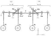
図1は本発明の実施例1の主走査方向の要部断面図(主走査断面図)である。図2は本発明の実施例1の副走査方向の要部断面図(副走査断面図)である。図3は本発明の実施例1の偏向手段より光源手段側の副走査断面図である。 FIG. 1 is a sectional view (main scanning sectional view) of the main part in the main scanning direction of the first embodiment of the present invention. FIG. 2 is a sectional view (sub-scanning sectional view) of the main part in the sub-scanning direction according to the first embodiment of the present invention. FIG. 3 is a sub-scan sectional view of the light source means side of the deflecting means according to the first embodiment of the present invention.
尚、以下の説明において、主走査方向(Y方向)とは偏向手段の回転軸及び結像光学手段の光軸(X方向)に垂直な方向(偏向手段で光束が偏向反射(偏向走査)される方向)である。副走査方向(Z方向)とは偏向手段の回転軸と平行な方向である。主走査断面とは結像光学手段の光軸と主走査方向とを含む平面である。副走査断面とは結像光学手段の光軸を含み主走査断面に垂直な断面である。 In the following description, the main scanning direction (Y direction) is a direction perpendicular to the rotation axis of the deflecting means and the optical axis (X direction) of the imaging optical means (the light flux is deflected and reflected (deflected and scanned) by the deflecting means). Direction). The sub-scanning direction (Z direction) is a direction parallel to the rotation axis of the deflecting unit. The main scanning section is a plane including the optical axis of the imaging optical means and the main scanning direction. The sub-scanning section is a section that includes the optical axis of the imaging optical means and is perpendicular to the main scanning section.
図中、1a〜1dは各々発光部(発光点)を有する光源手段であり、例えば半導体レーザーよって成っている。2a〜2dは各々絞りであり、光束(光量)を制限している。
In the figure,
3は光束変換手段である。光束変換手段3は複数の光源手段1a〜1dから出射した複数の光束の集光状態を変換する機能と、光束を偏向手段5の偏向面において主走査方向に延伸した線像に変換する機能とを有する複数の光学素子3a〜3dを一体形成して構成されている。
本実施例における光束変換手段3を構成する複数の光学素子3a〜3dの光軸は、主走査断面内において、偏心している。
The optical axes of the plurality of
尚、絞り2a〜2d及び光束変換手段3の各要素はそれぞれ入射光学系(集光光学系)La〜Ldの一要素を構成している。
Each element of the
5は偏向手段(偏向素子)としての光偏向器であり、複数の偏向面を有する回転多面鏡(ポリゴンミラー)よりなり、モータ等の駆動手段により矢印A方向に等速で回転しており、入射光学系La〜Ldからの光束を偏向走査している。
An
6a〜6dは各々結像光学系としての結像光学手段であり、偏向手段5からの複数の光束を各光束毎に対応した被走査面8a〜8d上に結像させる。ステーション(走査ユニット)SR側の結像光学手段6a、6bは、各々共通の第1の結像レンズ61abと第2の結像レンズ62a、62bを有している。ステーションSL側の結像光学手段6c、6dは、各々共通の第1の結像レンズ61cdと第2の結像レンズ62c、62dを有している。
結像光学手段6a〜6dは、各々光偏向器5によって偏向反射された画像情報に基づく光束を対応する被走査面としての感光ドラム面8a〜8d上に結像させている。かつ結像光学手段6a〜6dは、各々副走査断面内において光偏向器5の偏向面51、52と感光ドラム面8a〜8dとの間を共役関係にすることにより偏向面51、52の面倒れ補償を行っている。
The imaging optical means 6a to 6d respectively form light beams based on image information deflected and reflected by the
7a,7b1,7b2は各々ステーションSR側のミラー(反射ミラー)であり、ステーションSR内で光路を折り曲げている。7c1、7c2,7dは各々ステーションSL側のミラー(反射ミラー)であり、ステーションSL内で光路を折り曲げている。8a,8bは各々ステーションSR側の被走査面としての感光ドラム面である。8c,8dは各々ステーションSL側の被走査面としての感光ドラム面である。
<走査光学装置>
本実施例の走査光学装置は4つの光源手段1a〜1dの発光部から出射した光束を異なる4つの被走査面8a〜8dに導光し、光走査するものである。以下、走査光学装置の機能説明においては簡単のため1つの光源手段1aからの光束について説明する。
<Scanning optical device>
The scanning optical apparatus of this embodiment guides the light beams emitted from the light emitting portions of the four light source means 1a to 1d to different four scanned
光源手段である半導体レーザ1aから出射した発散光束は絞り2aによって光量を制限され、対応する光束変換手段3の光学素子3aに入射する。光学素子3aは、光源手段1aからの光束を主走査断面内(主走査方向)に関しては平行光束に変換し、副走査断面内(副走査方向)に関しては偏向手段5の偏向面51に結像するよう光束の状態を変換している。
The divergent light beam emitted from the
偏向手段5に入射した光束は偏向面51により被走査面方向に偏向走査され、結像光学手段6aに入射する。本実施例において結像光学手段6aは主に主走査方向にパワーを有するプラスチック製の第1のトーリックレンズ(結像レンズ)61abと主に副走査方向にパワーを有するプラスチック製の第2のトーリックレンズ(結像レンズ)62aとより構成される。また結像光学手段6aは、偏向面51からの偏向光束を被走査面8aに結像させるとともに偏向面51の倒れを補償している。
The light beam incident on the deflecting means 5 is deflected and scanned in the direction of the surface to be scanned by the deflecting
本実施例における第1のトーリックレンズ61abは、上記の如く2組の結像光学手段6a、6bで共通に使用されている。なお、結像光学手段6aの形態、製法はこれに限定されるものではない。
The first toric lens 61ab in this embodiment is used in common by the two sets of imaging
上記結像光学手段6aにより被走査面8a上に結像した光束は、モータ軸(不図示)に取り付けられたポリゴンミラーの回転により被走査面8a上を矢印B方向(主走査方向)に等角速度で偏向走査する。
The light beam imaged on the scanned
<タンデム型の走査光学装置>
本実施例における走査光学装置はこれらの走査機能を4つ有することで、異なる色相に対応する画像情報を同時に異なる被走査面上に記録するタンデム型の走査光学装置であり、以下、それについて、詳細に説明する。
<Tandem scanning optical device>
The scanning optical device in this embodiment is a tandem scanning optical device that has four of these scanning functions, and simultaneously records image information corresponding to different hues on different surfaces to be scanned. This will be described in detail.
図1、図3に示すとおり、本実施例における4つの光源手段1a〜dは各々主走査方向及び副走査方向に離間して配列されている。 As shown in FIGS. 1 and 3, the four light source means 1a to 1d in the present embodiment are arranged separately in the main scanning direction and the sub-scanning direction, respectively.
このうち光源手段1a、1bの発光部から出射した光束を偏向手段5の偏向面51へ、光源手段1c、1dの発光部から出射した光束を偏向手段5の偏向面52へ入射させ、それぞれの光束を偏向手段5の左右に分離している。
Of these, the light beams emitted from the light emitting sections of the light source means 1a and 1b are incident on the deflecting
さらに光源手段1a、1bの発光部から出射した光束は、副走査断面内で異なる入射角をもち、偏向手段5の偏向面51に対して斜入射させることにより、第1のトーリックレンズ61ab後に配置したミラー7b1により空間分離している。尚、光源手段1c、1dの発光部から出射した光束に関しても同様である。
Further, the light beams emitted from the light emitting sections of the light source means 1a and 1b have different incident angles in the sub-scan section and are obliquely incident on the deflecting
このように偏向手段(ポリゴンミラー)5に対し異なる斜入射角を有する複数の光束を、該偏向手段5の異なる2つの偏向面51,52に入射させることにより、一つの偏向手段5で4つの光束を同時に走査可能としている。 In this way, a plurality of light beams having different oblique incident angles with respect to the deflecting means (polygon mirror) 5 are incident on two different deflecting surfaces 51 and 52 of the deflecting means 5, so that one deflecting means 5 The light beam can be scanned simultaneously.
<光束変換手段>
次に本実施例における光束変換手段3及びそれを構成する光学素子3aに関し説明する。
<Flux conversion means>
Next, the light beam conversion means 3 and the
光学素子3aは、光源手段1aの発光部からの光束を平行光束化するコリメータレンズとしての機能を有している。さらに光学素子3aは、コリメータレンズとしての機能と、光束を偏向手段5の偏向面51において主走査方向に延伸した線像に変換するアナモフィックコリメータレンズ(シリンドリカルレンズ)としての機能とを複合化させたものである。
The
光束変換手段3は、プラスチックモールド製の光学素子より成っており、1つの光学素子3でコリメータレンズ4枚、シリンドリカルレンズ4枚分の機能を有している。 The light beam conversion means 3 is made of an optical element made of plastic mold, and has a function corresponding to four collimator lenses and four cylindrical lenses.
これにより光学系の簡素化はもちろんのこと、装置の組立性の向上や、小型化にも充分寄与するものとなっている。 This contributes not only to the simplification of the optical system but also to the improvement of the assembly of the apparatus and the miniaturization.
表1に本実施例における光源手段から偏向手段までの設計値を示す。光学素子(アナモフィックコリメータレンズ)3aの入射面(光源手段側面)は主走査方向と副走査方向とで異なるパワーを有する回折格子をその光学面上に有する回折面より成る。また出射面は主走査方向と副走査方向とで異なるパワーを有する屈折面、つまりアナモフィック面より成る。 Table 1 shows design values from the light source means to the deflection means in this embodiment. The incident surface (side surface of the light source means) of the optical element (anamorphic collimator lens) 3a is composed of a diffraction surface having a diffraction grating having different powers in the main scanning direction and the sub-scanning direction on the optical surface. The exit surface is composed of a refracting surface having different powers in the main scanning direction and the sub-scanning direction, that is, an anamorphic surface.
ここで入射面に回折面を用いているのは、昇温により発生するプラスチック材料の屈折率変化によるパワー変化を補正するためである。同じく昇温により発生する波長変化によるパワー変化、つまり回折面による強い軸上色収差で補正するためである。 The reason why the diffractive surface is used as the incident surface is to correct the power change due to the refractive index change of the plastic material generated by the temperature rise. This is also to correct for power change due to wavelength change caused by temperature rise, that is, strong axial chromatic aberration due to the diffraction surface.
ここで本実施例の回折面はベース屈折面上に以下の位相関数で表される回折格子を付加した形状である。 Here, the diffraction surface of the present embodiment has a shape in which a diffraction grating represented by the following phase function is added to the base refractive surface.
φ=mλ=d2mY2+d2sZ2
(但しmは回折次数で、本実施例は+1次光を使用)
図4は走査光学装置の結像位置(ピント)の温度依存性を示す図、図5は同じく波長依存性を示す図である。両図において点線は主走査方向のピント位置、実線は副走査方向のピント位置を示している。
φ = mλ = d 2m Y 2 + d 2s Z 2
(Where m is the diffraction order, and this embodiment uses + 1st order light)
FIG. 4 is a diagram showing the temperature dependence of the imaging position (focus) of the scanning optical device, and FIG. 5 is a diagram showing the wavelength dependence. In both figures, the dotted line indicates the focus position in the main scanning direction, and the solid line indicates the focus position in the sub-scanning direction.
図4より光束変換手段3に回折面を用いることにより、温度変化に伴うピント移動は1/5以下(対回折面を用いなかった場合)に抑えられていることが読み取れる。また本実施例では光源手段と被走査面との間で定義される主走査方向の縦倍率αmを特定の値(100倍)より小さく設定することにより、光源手段と光束変換手段3との間の距離が変動による被走査面上でのピント変化を低減している。 It can be seen from FIG. 4 that the use of a diffractive surface for the light beam conversion means 3 suppresses the focus movement accompanying the temperature change to 1/5 or less (when no anti-diffraction surface is used). In this embodiment, the vertical magnification αm in the main scanning direction defined between the light source means and the surface to be scanned is set smaller than a specific value (100 times), so that the distance between the light source means and the light beam conversion means 3 is set. The focus change on the surface to be scanned due to the fluctuation of the distance is reduced.
つまり、本実施例では、光源手段の発光部と被走査面間における主走査断面内の縦倍率をαmとするとき、
αm<100 …(1)
なる条件を満足するように設定している。
That is, in this embodiment, when the vertical magnification in the main scanning section between the light emitting portion of the light source means and the scanned surface is αm,
αm <100 (1)
Is set to satisfy the following conditions.
尚、縦倍率αmの下限値は、
10<αm …(1a)
とするのが良い。
The lower limit of the vertical magnification αm is
10 <αm (1a)
It is good to do.
一方で図5に示すとおり、初期波長ばらつき等の屈折率変動を伴わない波長変化によるピント変動は従来と比較して大きくなるが、これは後に説明するレーザピント調整により調整することが可能であり、問題とならない。 On the other hand, as shown in FIG. 5, the focus fluctuation due to the wavelength change not accompanied by the refractive index fluctuation such as the initial wavelength fluctuation becomes larger than the conventional one, but this can be adjusted by the laser focus adjustment described later. No problem.
このように本実施例では回折面を用いることにより、光束変換手段3をプラスチック材料で製作した場合においても、昇温によるピント変化を実用上問題のない量まで低減している。
As described above, in this embodiment, by using the diffractive surface, even when the light
なお、本実施例ではプラスチックモールド製の光束変換手段3の例を挙げ説明したが、環境変化に対してより安定なガラスモールド製の光束変換手段より構成しても良い。 In this embodiment, an example of the light flux conversion means 3 made of plastic mold has been described. However, the light flux conversion means made of glass mold that is more stable against environmental changes may be used.
またシリンドリカルレンズの機能を有さない通常のコリメータレンズでも本発明の効果を得ることができる。 The effect of the present invention can also be obtained with a normal collimator lens that does not have a cylindrical lens function.

<レーザ調整>
次に本実施例における光源手段1a〜1d、及びその調整方法の説明をする。
<Laser adjustment>
Next, the light source means 1a to 1d and the adjustment method thereof in this embodiment will be described.
光源手段である半導体レーザと光束変換手段 (以下、「コリメータレンズ」とも称す。)は以下の調整(レーザ調整)を行う必要がある。 The semiconductor laser that is the light source means and the light beam conversion means (hereinafter also referred to as “collimator lens”) need to be adjusted as follows (laser adjustment).
ピント調整工程:出射光束が特定の平行光束、あるいは収束光束、発散光束となるよう、半導体レーザとコリメータレンズ間の距離を調整する。 Focus adjustment step: The distance between the semiconductor laser and the collimator lens is adjusted so that the emitted light beam becomes a specific parallel light beam, a convergent light beam, or a divergent light beam.
照射位置調整工程:出射光束が特定のターゲットに照射するよう、半導体レーザとコリメータレンズ間の同軸度(光軸に垂直な方向の位置)を調整する。 Irradiation position adjustment step: The coaxiality (position in the direction perpendicular to the optical axis) between the semiconductor laser and the collimator lens is adjusted so that the emitted light beam irradiates a specific target.
ピッチ間隔調整工程:マルチビーム走査光学装置の場合、被走査面上で複数の光束のピッチ間隔が特定の値となるよう、半導体レーザを出射軸中心に回転させ調整する。 Pitch interval adjustment step: In the case of a multi-beam scanning optical device, the semiconductor laser is rotated and adjusted around the emission axis so that the pitch intervals of a plurality of light beams have a specific value on the surface to be scanned.
これらの調整は光学的には半導体レーザ、コリメータレンズのどちらを移動させても同じであるが、半導体レーザは半田付け等で電気基板に取付ける必要があるため、より調整しやすいコリメータレンズ側を移動させることが一般的である。 These adjustments are optically the same regardless of whether the semiconductor laser or the collimator lens is moved, but the semiconductor laser must be attached to the electrical board by soldering, etc., so the collimator lens side is easier to adjust. It is common to make it.
しかしながら本実施例においては、コリメータレンズ側が4つの光学素子を一体構造としているため個別に位置を調整することは困難である。 However, in this embodiment, it is difficult to adjust the position individually because the collimator lens side has four optical elements as an integral structure.
そこで本実施例においては複数の半導体レーザ1a〜1dを各々対応する光学素子3a〜3dに対する位置を調整することにより、該半導体レーザ1a〜1dのピント及び照射位置を調整し、その後、同一の保持部材に固定している。
Therefore, in this embodiment, by adjusting the positions of the plurality of
図6に本実施例における光源手段1及び光束変換手段3の要部概略図を示し、レーザ調整機構に関し説明する。 FIG. 6 shows a schematic diagram of the main parts of the light source means 1 and the light beam conversion means 3 in this embodiment, and the laser adjustment mechanism will be described.
光源手段である半導体レーザ1a〜1dのレーザパッケージはレーザ鏡筒11a〜11dに圧入されており、不図示である治工具で把持されている。この状態において半導体レーザ1a〜1dを発光させ、該レーザ1a〜1dのピント並びに照射位置が特定の位置となるよう、レーザ鏡筒11a〜11dの光軸方向並びにそれと垂直な方向の位置を調整する。尚、マルチビーム走査光学装置の場合は、半導体レーザの出射軸を回転中心として回転調整する。
Laser packages of the
このときのレーザのピント、照射位置の測定方法は光偏向器を除去し治具レンズを挿入した状態でチャート面のピント位置、照射位置を測定する方法、実際に使用する結像光学素子を介してピント、照射位置を測定する方法等があり、何れの方法でも良い。 At this time, the laser focus and irradiation position are measured by a method of measuring the focus position and irradiation position of the chart surface with the optical deflector removed and the jig lens inserted, and through an imaging optical element actually used. There are methods for measuring the focus and irradiation position, and any method may be used.
レーザ鏡筒11a〜11dの位置が決まり次第、該レーザ鏡筒11a〜11dと光学箱のレーザ鏡筒保持部12との隙間に予め塗布されたUV硬化型接着剤13にUV光(紫外線)を照射し、接着剤を固化させ固定する。
As soon as the positions of the laser barrels 11a to 11d are determined, UV light (ultraviolet rays) is applied to the UV
このように本実施例では4つの半導体レーザ1a〜1dが、それぞれのレーザ鏡筒11a〜11dを介して同一の保持部材としての光学箱のレーザ鏡筒保持部12に一体的に取り付けられている。これにより各々の半導体レーザ1a〜1dを駆動する基板の一体化も可能となる。
As described above, in this embodiment, the four
このような調整を行うにあたっては半導体レーザにレーザ鏡筒を把持する治工具のスペース、UV光を照射するファイバーを配置するスペース等を確保しておく必要がある。これら空間を確保した上で精度良くレーザ調整を行うためには、主走査方向、副走査方向の少なくともどちらか一方の光源手段間の間隔を実際に使用する半導体レーザのパッケージの最大外形以上確保する必要がある。 In performing such adjustment, it is necessary to secure a space for a jig for holding the laser barrel, a space for arranging a fiber for irradiating UV light, and the like to the semiconductor laser. In order to perform laser adjustment with high accuracy while ensuring these spaces, the interval between the light source means in at least one of the main scanning direction and the sub-scanning direction is ensured to be equal to or larger than the maximum outline of the semiconductor laser package to be actually used. There is a need.
つまり複数の光源手段の発光部の主走査方向の間隔をLm、副走査方向の間隔をLs、1つの光源手段のパッケージの最大外形をPとするとき、
Max(Lm、Ls)>2P …(2)
なる条件を満足させる必要がある。
That is, when the interval in the main scanning direction of the light emitting units of the plurality of light source means is Lm, the interval in the sub scanning direction is Ls, and the maximum outer shape of the package of one light source means is P,
Max (Lm, Ls)> 2P (2)
It is necessary to satisfy the following conditions.
尚、Max(Lm、Ls)は、間隔Lm、Lsのうち、長い方の値を取ることを意味している。従って(2)式は2P<Lm、又は2P<Lsの少なくとも一方を満足する。 Note that Max (Lm, Ls) means taking the longer value of the intervals Lm and Ls. Therefore, the formula (2) satisfies at least one of 2P <Lm and 2P <Ls.
本実施例では副走査方向の斜入射角θsをθs=5°と大きくとることにより、半導体レーザのパッケージの最大外形P=5.6に対して、光源手段間の副走査方向の間隔LsをLs=19.87と大きく確保している。これにより従来困難とされてきた複数の光源手段を有する光学系における光源手段側を可動にしたレーザ調整が可能となり、複眼(4眼)を一体化した光束変換手段3の使用を実現している。 In this embodiment, the oblique incident angle θs in the sub-scanning direction is set as large as θs = 5 °, so that the distance Ls in the sub-scanning direction between the light source means with respect to the maximum outer shape P = 5.6 of the semiconductor laser package. Ls = 19.87 is secured. This makes it possible to perform laser adjustment by moving the light source means side in an optical system having a plurality of light source means, which has been considered difficult in the past, and realizes the use of the light beam conversion means 3 in which the compound eyes (four eyes) are integrated. .
なお、本実施例では光学箱のレーザ鏡筒取り付け部12にレーザ鏡筒11a〜11dを直接取り付けたが、これに限ることはない。例えば複数のレーザ鏡筒11a〜11dを同時に保持するサブユニット(所謂レーザユニット)を作成し、その状態でレーザ調整をした後、光学箱に組み込んでも同様の効果を得ることができる。
In this embodiment, the laser barrels 11a to 11d are directly attached to the laser
このように本実施例においては、複数の光源手段1a〜1dからの光束の集光状態を変換する複数の光学素子3a〜3dを一体形成すると共に複数の光源手段1a〜1dを各々対応する光学素子3a〜3dに対しその位置を調整した後、固定している。これによりタンデム型の走査光学装置の全ての部品(光源手段、光束変換手段)におけるステーション間の一体化を図ることが可能となり、光学性能を損なうことなく組立性の向上を実現することができる。
As described above, in this embodiment, a plurality of
さらにこの走査光学装置により高精細印字が可能なカラー画像形成装置を実現することができる。 Furthermore, a color image forming apparatus capable of high-definition printing can be realized by this scanning optical device.
図7は本発明の実施例2の走査光学装置の主走査方向の要部断面図(主走査断面図)である。図8は本発明の実施例2の偏向手段以前の副走査方向の要部断面図であり、偏向手段以降の副走査断面は実施例1の断面図である図2と同一である。図7、図8において図1、図3に示した要素と同一要素には同符番を付している。 FIG. 7 is a sectional view (main scanning sectional view) of the main part in the main scanning direction of the scanning optical apparatus according to the second embodiment of the present invention. FIG. 8 is a cross-sectional view of the main part in the sub-scanning direction before the deflecting unit according to the second embodiment of the present invention, and the sub-scan section after the deflecting unit is the same as FIG. 7 and 8, the same elements as those shown in FIGS. 1 and 3 are denoted by the same reference numerals.
本実施例において、前述の実施例1と異なる点は、複数の光源手段1a〜4dの発光部から偏向手段5に向かう光束のうち、偏向手段5の異なる偏向面へ入射する光束を主走査断面内で非対称にした点である。さらに、それに伴い副走査方向の斜入射角θsを設定した点である。その他の構成及び光学的作用は実施例1と同様であり、これにより同様な効果を得ている。 In the present embodiment, the difference from the first embodiment described above is that a light beam incident on a different deflection surface of the deflecting means 5 out of the light fluxes directed from the light emitting portions of the plurality of light source means 1a to 4d to the deflecting means 5 is a main scanning section. It is the point which made it asymmetric. Further, the oblique incident angle θs in the sub-scanning direction is set accordingly. Other configurations and optical functions are the same as those in the first embodiment, and the same effects are obtained.
つまり本実施例においては、複数の光源手段1a〜4dの主走査方向の発光部間隔を広く取るために、複数の発光部から偏向手段5に向かう光束のうち、偏向手段5の異なる偏向面へ入射する光束を主走査断面内で非対称にしている。さらに本実施例では、それに伴い副走査方向の斜入射角θsを実施例1より小さく設定している。
That is, in the present embodiment, in order to increase the interval between the light emitting units in the main scanning direction of the plurality of
表2に本実施例における光源手段から偏向手段までの設計値を示す。本実施例においても光学素子の入射面(光源手段側面)は主走査方向と副走査方向とで異なるパワーを有する回折面である。また光学素子の出射面は主走査方向と副走査方向とで異なるパワーを有する屈折面、つまりアナモフィック面である。 Table 2 shows design values from the light source means to the deflection means in this embodiment. Also in this embodiment, the incident surface (light source means side surface) of the optical element is a diffractive surface having different powers in the main scanning direction and the sub-scanning direction. The exit surface of the optical element is a refracting surface having different powers in the main scanning direction and the sub-scanning direction, that is, an anamorphic surface.
図9に本実施例における光源手段1及び光束変換手段3の要部概略図を示す。同図において図6に示した要素と同一要素には同符番を付している。 FIG. 9 shows a schematic diagram of the main parts of the light source means 1 and the light beam conversion means 3 in this embodiment. In the figure, the same elements as those shown in FIG.
本実施例においても前述の実施例1と同様、光源手段1a〜1dにレーザ鏡筒11a〜11dを把持する治工具のスペース、UV光を照射するファイバーを配置するスペース等を確保しておく必要がある。これら空間を確保した上で精度良くレーザ調整を行うためには、主走査方向、副走査方向どちらか一方の光源手段間の間隔を実際に使用する半導体レーザのパッケージの最大外形以上確保する必要がある。 In the present embodiment as well, as in the first embodiment, it is necessary to secure a space for jigs holding the laser barrels 11a to 11d, a space for arranging a fiber for irradiating UV light, etc. in the light source means 1a to 1d. There is. In order to perform laser adjustment with high accuracy while ensuring these spaces, it is necessary to ensure that the distance between the light source means in either the main scanning direction or the sub-scanning direction is larger than the maximum outer shape of the semiconductor laser package that is actually used. is there.
そこで本実施例では光源手段1a〜1dから偏向手段5に向かう光束のうち、異なる偏向面へ入射する光束同士を主走査方向に非平行にすることにより、主走査方向の発光部間隔を確保している。
Therefore, in this embodiment, among the light beams directed from the
ここで偏向手段5の異なる偏向面へ入射する2つの光束が主走査断面内において、なす角度をθmi(°)とするとき、以下の条件式(3)を満足することが望ましい。
Here, it is desirable that the following conditional expression (3) is satisfied when an angle formed by two light beams incident on different deflecting surfaces of the deflecting
1°<θmi<10° …(3)
条件式(3)は角度θmiを規定する条件である。条件式(3)の下限値を越えると複数の光源手段1a〜1dの発光部間隔を充分に確保することが難しくなり、また条件式(3)の上限値を越えると両者の光束が離れすぎ、コリメータレンズの一体化や複数の光源手段1a〜1dの一体保持が困難となる。
1 ° <θmi <10 ° (3)
Conditional expression (3) is a condition for defining the angle θmi. If the lower limit value of conditional expression (3) is exceeded, it will be difficult to ensure a sufficient interval between the light emitting sections of the light source means 1a to 1d. It becomes difficult to integrate the collimator lens and to integrally hold the plurality of light source means 1a to 1d.
さらに望ましくは、上記条件式(3)を次の如く設定するのが良い。 More preferably, the conditional expression (3) should be set as follows.
2°<θmi<9° …(3a)
また主走査断面内において、光束変換手段3を構成する複数の光学素子3a〜3dの入射面の中心間隔をCm、複数の光源手段1a〜1dの発光部の間隔をLmとするとき、以下の条件式(4)を満足することが望ましい。
2 ° <θmi <9 ° (3a)
In the main scanning section, when the center distance between the incident surfaces of the plurality of
Cm<Lm …(4)
条件式(4)は複数の光学素子の入射面の中心間隔Cmと複数の光源手段の発光部の間隔Lmの大小関係を規定しものである。条件式(4)を外れると複数の光源手段1a〜1dの発光部の主走査方向の間隔Lmが狭くなり、光源手段側でのレーザ調整が困難となる。
Cm <Lm (4)
Conditional expression (4) defines the size relationship between the center distance Cm of the incident surfaces of the plurality of optical elements and the distance Lm of the light emitting sections of the plurality of light source means. If the conditional expression (4) is not satisfied, the interval Lm in the main scanning direction of the light emitting units of the plurality of
本実施例においては、偏向手段5へ入射する光束の主光線と結像光学手段の光軸とがなす角θmを
θm=86°
に設定することで、両光束が主走査方向になす角度θmiを
θmi=8°
としている。また上記複数の光学素子3a〜3dの入射面の中心間隔Cm及び複数の光源手段1a〜1dの発光部の間隔Lmを
Cm=13.33、
Lm=15.88
となるよう非平行の方向性を設定し、かつ前述した条件式(2)も満足させている。
In this embodiment, the angle θm formed by the principal ray of the light beam incident on the deflecting means 5 and the optical axis of the imaging optical means is θm = 86 °.
By setting to, the angle θmi formed by both beams in the main scanning direction is θmi = 8 °
It is said. Further, the center distance Cm of the incident surfaces of the plurality of
Lm = 15.88
The non-parallel directionality is set so as to satisfy the above condition and the conditional expression (2) described above is also satisfied.
これにより本実施例では、コリメータレンズの一体化や複数の光源手段1a〜1dの一体保持を実現しつつ、光源手段側でのレーザ調整を可能とする主走査方向の発光部間隔を確保している。
Thus, in this embodiment, the collimator lens is integrated and the plurality of
また主走査方向に充分な間隔を確保したため、副走査方向の間隔Lsを
Ls=11.93
と小さく、つまり副走査方向の斜入射角θsを実施例1より小さく設定することが可能となった。因みに本実施例の斜入射角θsは表2に示す如くθs=3°である。
Further, since a sufficient interval is ensured in the main scanning direction, the interval Ls in the sub-scanning direction is set to Ls = 11.93.
In other words, the oblique incident angle θs in the sub-scanning direction can be set smaller than that in the first embodiment. Incidentally, the oblique incident angle θs of the present embodiment is θs = 3 ° as shown in Table 2.
このように本実施例においては、複数の光源手段1a〜1dからの光束の集光状態を変換する複数の光学素子3a〜3dを一体形成すると共に複数の光源手段1a〜1dを各々対応する光学素子3a〜3dに対しその位置を調整した後、固定している。これによりタンデム型の走査光学装置の全ての部品(光源手段、光束変換手段)におけるステーション間の一体化を図ることが可能となり、光学性能を損なうことなく組立性の向上を実現することができる。
As described above, in this embodiment, a plurality of
さらにこの走査光学装置により高精細印字が可能なカラー画像形成装置を実現することができる。 Furthermore, a color image forming apparatus capable of high-definition printing can be realized by this scanning optical device.
さらに本実施例固有の特徴として、複数の光源手段の主走査方向の間隔を広くすることにより、相対的に副走査方向のスペースを狭くすることができ、副走査方向の斜入射角の低減による光学特性の向上も実現することができる。 Furthermore, as a feature unique to the present embodiment, the space in the main scanning direction of the plurality of light source means is widened, so that the space in the sub scanning direction can be relatively narrowed, and the oblique incident angle in the sub scanning direction is reduced. Improvement of optical characteristics can also be realized.
<カラー画像形成装置>
図10は本発明の実施例のカラー画像形成装置の要部概略図である。図10において、160はカラー画像形成装置、110は各々実施例1,2に示した構成を有する走査光学装置、121,122,123,124は各々像担持体としての感光ドラム、131,132,133,134は各々現像器、151は搬送ベルトである。
<Color image forming apparatus>
FIG. 10 is a schematic view of a main part of a color image forming apparatus according to an embodiment of the present invention. In FIG. 10, 160 is a color image forming apparatus, 110 is a scanning optical device having the structure shown in each of
図10において、カラー画像形成装置160には、パーソナルコンピュータ等の外部機器152からR(レッド)、G(グリーン)、B(ブルー)の各色信号が入力する。これらの色信号は、装置内のプリンタコントローラ153によって、C(シアン),M(マゼンタ),Y(イエロー)、B(ブラック)の各画像データ(ドットデータ)に変換される。これらの画像データは、それぞれ走査光学装置110に入力される。そして、これらの走査光学装置からは、各画像データに応じて変調された光ビーム141,142,143,144が出射され、これらの光ビームによって感光ドラム121,122,123,124の感光面が主走査方向に走査される。
In FIG. 10, the color
本実施例におけるカラー画像形成装置は上述の如く走査光学装置110からの各々の画像データに基づいた4本の光ビームを用いて各色の潜像を各々対応する感光ドラム121,122,123,124面上に形成している。その後、記録材に多重転写して1枚のフルカラー画像を形成している。
The color image forming apparatus in this embodiment forms latent images of each color on the corresponding
前記外部機器152としては、例えばCCDセンサを備えたカラー画像読取装置が用いられても良い。この場合には、このカラー画像読取装置と、カラー画像形成装置160とで、カラーデジタル複写機が構成される。
As the
1a〜1d 光源手段(半導体レーザ)
2a〜2d 開口絞り
3 光束変換手段(アナモフィックコリメータレンズ)
3a〜3d 光学素子
5 偏向手段(ポリゴンミラー)
51、52 偏向面
6a〜6d 結像光学手段(fθレンズ系)
61ab,61cd 第1トーリックレンズ
62a〜62d 第2トーリックレンズ
8a〜8d 被走査面(感光ドラム面)
11a〜11d レーザ鏡筒
12 光学箱レーザ鏡筒保持部
13 UV硬化型接着剤
1a to 1d Light source means (semiconductor laser)
2a to 2d Aperture stop 3 Luminous flux conversion means (anamorphic collimator lens)
3a to 3d
51, 52
61ab, 61cd First
11a to
Claims (3)
前記複数の光源手段は、主走査方向及び副走査方向に離間して配列されており、
前記光束変換手段は、前記複数の光源手段から出射された複数の光束に対応して配置され前記複数の光束の各々の光束の集光状態を変換する複数の光学素子を一体形成して構成されており、
前記複数の光源手段は、同一の保持部材に固定されており、
主走査断面内において、前記光束変換手段を構成する複数の光学素子の入射面の主走査方向の中心間隔をCm、前記複数の光源手段の主走査方向の間隔をLm、前記複数の光源手段の1つの光源手段のパッケージの最大外形をPとするとき、
Cm < Lm and Lm > 2P
を満たすことを特徴とする走査光学装置。 A plurality of light source means, a light beam converting means for converting a light collecting state of a plurality of light beams emitted from the plurality of light source means, and a plurality of light beams emitted from the light beam converting means and incident on different deflection surfaces are deflected and scanned. A scanning optical apparatus comprising: a deflecting unit configured to form a plurality of light beams deflected and scanned by different deflecting surfaces of the deflecting unit; and an imaging optical unit configured to form an image on a scanned surface corresponding to each light beam.
The plurality of light source means are arranged separately in the main scanning direction and the sub-scanning direction,
The light beam converting means is formed by integrally forming a plurality of optical elements that are arranged corresponding to the plurality of light beams emitted from the plurality of light source means and convert the light collection state of each of the plurality of light beams. And
The plurality of light source means are fixed to the same holding member,
Within the main scanning section, the center interval in the main scanning direction of the incident surfaces of the plurality of optical elements constituting the light beam converting unit is Cm, the interval in the main scanning direction of the plurality of light source units is Lm, and When the maximum outer shape of the package of one light source means is P,
Cm <Lm and Lm> 2P
A scanning optical device characterized by satisfying the above.
Priority Applications (4)
| Application Number | Priority Date | Filing Date | Title |
|---|---|---|---|
| JP2007263058A JP4958714B2 (en) | 2007-10-09 | 2007-10-09 | Scanning optical device and image forming apparatus using the same |
| US12/244,718 US8154706B2 (en) | 2007-10-09 | 2008-10-02 | Scanning optical device, image forming apparatus using the same, and method of adjusting scanning optical device |
| EP08017634A EP2053446A1 (en) | 2007-10-09 | 2008-10-08 | Scanning optical device, image forming apparatus using the same, and method of adjusting scanning optical device |
| CN2008101702078A CN101408670B (en) | 2007-10-09 | 2008-10-09 | Scanning optical device, image forming apparatus using the same, and method of adjusting scanning optical device |
Applications Claiming Priority (1)
| Application Number | Priority Date | Filing Date | Title |
|---|---|---|---|
| JP2007263058A JP4958714B2 (en) | 2007-10-09 | 2007-10-09 | Scanning optical device and image forming apparatus using the same |
Publications (3)
| Publication Number | Publication Date |
|---|---|
| JP2009092916A JP2009092916A (en) | 2009-04-30 |
| JP2009092916A5 JP2009092916A5 (en) | 2010-11-25 |
| JP4958714B2 true JP4958714B2 (en) | 2012-06-20 |
Family
ID=40428020
Family Applications (1)
| Application Number | Title | Priority Date | Filing Date |
|---|---|---|---|
| JP2007263058A Active JP4958714B2 (en) | 2007-10-09 | 2007-10-09 | Scanning optical device and image forming apparatus using the same |
Country Status (4)
| Country | Link |
|---|---|
| US (1) | US8154706B2 (en) |
| EP (1) | EP2053446A1 (en) |
| JP (1) | JP4958714B2 (en) |
| CN (1) | CN101408670B (en) |
Families Citing this family (22)
| Publication number | Priority date | Publication date | Assignee | Title |
|---|---|---|---|---|
| JP5072613B2 (en) * | 2008-01-18 | 2012-11-14 | キヤノン株式会社 | Optical scanning device and image forming apparatus using the same |
| JP2011033769A (en) * | 2009-07-31 | 2011-02-17 | Canon Inc | Scanning optical apparatus and image forming apparatus using the same |
| KR101599887B1 (en) | 2009-10-07 | 2016-03-04 | 삼성전자주식회사 | Light scanning unit and electrophotograpohic image forming apparatus using the same |
| JP5691528B2 (en) * | 2011-01-07 | 2015-04-01 | 株式会社リコー | Optical scanning apparatus and image forming apparatus |
| DK2726264T3 (en) * | 2011-06-28 | 2017-02-27 | Global Filtration Systems Dba Gulf Filtration Systems Inc | Apparatus for forming three-dimensional objects using an ultraviolet laser diode |
| US9075409B2 (en) | 2011-06-28 | 2015-07-07 | Global Filtration Systems | Apparatus and method for forming three-dimensional objects using linear solidification |
| JP5882646B2 (en) * | 2011-09-16 | 2016-03-09 | キヤノン株式会社 | Optical scanning apparatus and image forming apparatus |
| JP5780093B2 (en) * | 2011-09-30 | 2015-09-16 | ブラザー工業株式会社 | Scanning optical device |
| JP6013868B2 (en) * | 2012-10-17 | 2016-10-25 | シャープ株式会社 | Optical scanning device and image forming apparatus having the same |
| JP2015028572A (en) * | 2013-07-31 | 2015-02-12 | シャープ株式会社 | Optical scanner and image forming apparatus |
| US10144205B2 (en) | 2014-02-20 | 2018-12-04 | Global Filtration Systems | Apparatus and method for forming three-dimensional objects using a tilting solidification substrate |
| US11104117B2 (en) | 2014-02-20 | 2021-08-31 | Global Filtration Systems | Apparatus and method for forming three-dimensional objects using a tilting solidification substrate |
| US10011076B2 (en) | 2014-02-20 | 2018-07-03 | Global Filtration Systems | Apparatus and method for forming three-dimensional objects using a tilting solidification substrate |
| US9902112B2 (en) | 2015-04-07 | 2018-02-27 | Global Filtration Systems | Apparatus and method for forming three-dimensional objects using linear solidification and a vacuum blade |
| CN108184036B (en) * | 2017-04-11 | 2019-11-15 | 安徽省冠腾信息科技有限公司 | Convenient for the image-forming conversion equipment of integrally connected |
| WO2019139895A1 (en) | 2018-01-09 | 2019-07-18 | Innovusion Ireland Limited | Lidar detection systems and methods that use multi-plane mirrors |
| US11675050B2 (en) | 2018-01-09 | 2023-06-13 | Innovusion, Inc. | LiDAR detection systems and methods |
| JP7022626B2 (en) * | 2018-03-16 | 2022-02-18 | キヤノン株式会社 | Optical scanning device and image forming device |
| CN112585492A (en) | 2018-06-15 | 2021-03-30 | 图达通爱尔兰有限公司 | LIDAR system and method for focusing a range of interest |
| DE112019005684T5 (en) | 2018-11-14 | 2021-08-05 | Innovusion Ireland Limited | LIDAR SYSTEMS AND METHODS USING A MULTI-FACET MIRROR |
| TW202208828A (en) * | 2020-01-31 | 2022-03-01 | 安盟生技股份有限公司 | Illumination system with etendue-squeezing module and method thereof |
| CN113985603B (en) * | 2021-12-22 | 2022-04-22 | 苏州旭创科技有限公司 | Light beam scanning system |
Family Cites Families (11)
| Publication number | Priority date | Publication date | Assignee | Title |
|---|---|---|---|---|
| JP3291906B2 (en) | 1994-04-11 | 2002-06-17 | キヤノン株式会社 | Scanning optical device |
| JP2003185952A (en) | 2001-12-19 | 2003-07-03 | Canon Inc | Optical scanner and color image forming apparatus using the same |
| JP4227335B2 (en) * | 2002-01-31 | 2009-02-18 | キヤノン株式会社 | Optical scanning device and image forming apparatus using the same |
| JP2004070107A (en) | 2002-08-08 | 2004-03-04 | Canon Inc | Optical scanner and image forming apparatus using the same |
| JP4378082B2 (en) | 2002-12-03 | 2009-12-02 | キヤノン株式会社 | Scanning optical device and image forming apparatus using the same |
| JP4366074B2 (en) * | 2002-12-24 | 2009-11-18 | キヤノン株式会社 | Scanning optical system |
| JP4340515B2 (en) * | 2003-02-27 | 2009-10-07 | 株式会社リコー | Optical scanning apparatus and image forming apparatus |
| JP4568642B2 (en) | 2005-06-01 | 2010-10-27 | 株式会社リコー | Optical scanning device and image forming apparatus |
| JP2007121342A (en) * | 2005-10-25 | 2007-05-17 | Canon Inc | Scanning optical device and image forming apparatus |
| JP5493240B2 (en) | 2005-11-21 | 2014-05-14 | 株式会社リコー | Optical scanning apparatus and image forming apparatus |
| JP2008026570A (en) * | 2006-07-20 | 2008-02-07 | Ricoh Co Ltd | Multibeam optical scanner and image forming apparatus |
-
2007
- 2007-10-09 JP JP2007263058A patent/JP4958714B2/en active Active
-
2008
- 2008-10-02 US US12/244,718 patent/US8154706B2/en active Active
- 2008-10-08 EP EP08017634A patent/EP2053446A1/en not_active Withdrawn
- 2008-10-09 CN CN2008101702078A patent/CN101408670B/en active Active
Also Published As
| Publication number | Publication date |
|---|---|
| CN101408670B (en) | 2011-06-22 |
| EP2053446A1 (en) | 2009-04-29 |
| US8154706B2 (en) | 2012-04-10 |
| US20090091732A1 (en) | 2009-04-09 |
| CN101408670A (en) | 2009-04-15 |
| JP2009092916A (en) | 2009-04-30 |
Similar Documents
| Publication | Publication Date | Title |
|---|---|---|
| JP4958714B2 (en) | Scanning optical device and image forming apparatus using the same | |
| KR100485315B1 (en) | Scanning optical device and image forming apparatus using the same | |
| JP5489612B2 (en) | Scanning optical device and image forming apparatus using the same | |
| JP5046760B2 (en) | Optical scanning device and image forming apparatus using the same | |
| JP2003322814A (en) | Optical scanner and image forming apparatus | |
| JP2004070107A (en) | Optical scanner and image forming apparatus using the same | |
| JP4015249B2 (en) | Multi-beam exposure system | |
| KR100856154B1 (en) | Optical scanning apparatus and image-forming apparatus using the same | |
| JP2004070108A (en) | Optical scanner and image forming apparatus using the same | |
| JP5316759B2 (en) | Optical scanning device, adjustment method, and image forming apparatus | |
| US8350883B2 (en) | Scanning optical apparatus and image forming apparatus using same | |
| US5966232A (en) | Scanning optical system | |
| JP4455309B2 (en) | Optical scanning device and image forming apparatus using the same | |
| JP2010072050A (en) | Optical scanner and method of adjusting optical scanner | |
| JP4902279B2 (en) | Image forming apparatus | |
| JP4404667B2 (en) | Optical scanning device | |
| JP5787661B2 (en) | Scanning optical device and image forming apparatus using the same | |
| JP3320239B2 (en) | Scanning optical device | |
| JP2002303810A (en) | Optical scanner and image forming device using the same | |
| JP2007334203A (en) | Optical scanner and image forming apparatus | |
| JP5826365B2 (en) | Optical scanning device and image forming apparatus using the same | |
| JP6234085B2 (en) | Optical scanning device and image forming apparatus using the same | |
| JP2013033129A5 (en) | ||
| JP2006195236A (en) | Image forming apparatus and color image forming apparatus | |
| JP2007108766A (en) | Multibeam exposure apparatus |
Legal Events
| Date | Code | Title | Description |
|---|---|---|---|
| A521 | Request for written amendment filed |
Free format text: JAPANESE INTERMEDIATE CODE: A523 Effective date: 20101012 |
|
| A621 | Written request for application examination |
Free format text: JAPANESE INTERMEDIATE CODE: A621 Effective date: 20101012 |
|
| A977 | Report on retrieval |
Free format text: JAPANESE INTERMEDIATE CODE: A971007 Effective date: 20120213 |
|
| TRDD | Decision of grant or rejection written | ||
| A01 | Written decision to grant a patent or to grant a registration (utility model) |
Free format text: JAPANESE INTERMEDIATE CODE: A01 Effective date: 20120221 |
|
| A01 | Written decision to grant a patent or to grant a registration (utility model) |
Free format text: JAPANESE INTERMEDIATE CODE: A01 |
|
| A61 | First payment of annual fees (during grant procedure) |
Free format text: JAPANESE INTERMEDIATE CODE: A61 Effective date: 20120319 |
|
| FPAY | Renewal fee payment (event date is renewal date of database) |
Free format text: PAYMENT UNTIL: 20150330 Year of fee payment: 3 |
|
| R151 | Written notification of patent or utility model registration |
Ref document number: 4958714 Country of ref document: JP Free format text: JAPANESE INTERMEDIATE CODE: R151 |
|
| RD03 | Notification of appointment of power of attorney |
Free format text: JAPANESE INTERMEDIATE CODE: R3D03 |