JP4951973B2 - Display device and display method - Google Patents
Display device and display method Download PDFInfo
- Publication number
- JP4951973B2 JP4951973B2 JP2006002677A JP2006002677A JP4951973B2 JP 4951973 B2 JP4951973 B2 JP 4951973B2 JP 2006002677 A JP2006002677 A JP 2006002677A JP 2006002677 A JP2006002677 A JP 2006002677A JP 4951973 B2 JP4951973 B2 JP 4951973B2
- Authority
- JP
- Japan
- Prior art keywords
- display
- area
- luminance
- divided
- light emission
- Prior art date
- Legal status (The legal status is an assumption and is not a legal conclusion. Google has not performed a legal analysis and makes no representation as to the accuracy of the status listed.)
- Expired - Fee Related
Links
Images


Landscapes
- Control Of Indicators Other Than Cathode Ray Tubes (AREA)
- Liquid Crystal (AREA)
- Liquid Crystal Display Device Control (AREA)
- Transforming Electric Information Into Light Information (AREA)
Description
本発明は、例えば、液晶表示装置に適用して好適な表示装置及び表示方法の技術分野に関する。 The present invention relates to a technical field of a display device and a display method suitable for application to, for example, a liquid crystal display device.
表示装置、例えば、液晶表示装置は、液晶パネルの画素が発光しないため、液晶パネルの背面側にバックライトを配置し、そのバックライトで液晶パネルの背面を照明して画像を表示させるようにしている。 In a display device, for example, a liquid crystal display device, since the pixels of the liquid crystal panel do not emit light, a backlight is disposed on the back side of the liquid crystal panel, and the back surface of the liquid crystal panel is illuminated with the backlight to display an image. Yes.
従来、液晶表示装置においては、バックライトによって液晶パネルの表示画面全体を均一な明るさで照明し、液晶パネルの各画素の開口率を制御しバックライトから出射された光の遮蔽量を調整することにより、表示画面の各部において必要な輝度を得るようにしている。従って、例えば、表示画面全体が暗い場合においても、バックライトは設定可能な略最大の輝度で発光しており、バックライトが無駄に明るく発光し消費電力が大きいという問題がある。 Conventionally, in a liquid crystal display device, the entire display screen of the liquid crystal panel is illuminated with uniform brightness by a backlight, the aperture ratio of each pixel of the liquid crystal panel is controlled, and the shielding amount of light emitted from the backlight is adjusted. Thus, necessary brightness is obtained in each part of the display screen. Therefore, for example, even when the entire display screen is dark, the backlight emits light with substantially the maximum luminance that can be set, and there is a problem that the backlight emits light unnecessarily brightly and consumes a large amount of power.
このようなバックライトを備えた液晶表示装置の問題を解決するために、例えば、表示画面全体の表示輝度情報に基づいてバックライト全体の発光輝度を制御する方法が提案されている。 In order to solve the problem of the liquid crystal display device having such a backlight, for example, a method of controlling the light emission luminance of the entire backlight based on display luminance information of the entire display screen has been proposed.
また、バックライトを構成する各光源に対応させて表示画面を複数の領域に分割し、その分割領域ごとに必要とされる表示輝度に対応して、部分的に光源の発光輝度を抑制する方法が提案されている(例えば、特許文献1参照)。 Also, a method of dividing the display screen into a plurality of regions corresponding to each light source constituting the backlight, and partially suppressing the light emission luminance of the light source corresponding to the display luminance required for each divided region Has been proposed (see, for example, Patent Document 1).
尚、上記した「発光輝度」とは、光源から光が出射されるときの輝度を言い、上記した「表示輝度」とは、光源から出射された光が表示部(表示画面)を透過したときの輝度を言う(以下、同じ)。 The above “emission luminance” refers to the luminance when light is emitted from the light source, and the “display luminance” refers to when the light emitted from the light source passes through the display unit (display screen). Of the brightness (hereinafter the same).
図22は、このような制御方法の一例を概念的に示したものである。例えば、図22(a)に示すように、1画像(原画像)の略中央部に最も暗い楕円形状が表示され、その周囲において徐々に明るくなっている画像が表示されるとする。このような画像が表示される液晶表示装置のバックライトcが、図22(b)に示すように、縦横に分割されて配置された複数の光源d、d、・・・によって構成されているとすると、図22(a)に示す画像を表示する際には、表示輝度が最も低い個所に対応する光源d、dの発光輝度を抑制する。 FIG. 22 conceptually shows an example of such a control method. For example, as shown in FIG. 22 (a), it is assumed that the darkest oval shape is displayed in the approximate center of one image (original image), and an image that gradually becomes brighter is displayed around it. The backlight c of the liquid crystal display device on which such an image is displayed is composed of a plurality of light sources d, d,... Arranged vertically and horizontally as shown in FIG. Then, when the image shown in FIG. 22A is displayed, the light emission luminance of the light sources d and d corresponding to the place where the display luminance is the lowest is suppressed.
このようにバックライトcの発光輝度を部分的に抑制して画像の表示を行うことにより、無駄なバックライトの点灯を防止して消費電力の低減を図ることができる。 Thus, by displaying the image while partially suppressing the light emission luminance of the backlight c, it is possible to prevent unnecessary lighting of the backlight and reduce power consumption.
ところで、上記した従来の光源の制御方法においては、例えば、領域における中央の位置(図23に示す位置Pa)が最も表示輝度の高い部分である場合には、図23に示すように、光源の発光輝度Aを値Mに設定することにより、表示輝度が最も高い部分に対応した必要な表示輝度を確保することが可能である。
一方、隣接する領域の表示輝度が低い状態であるとすると、領域における境界の位置(図23に示す位置Pb)が最も表示輝度の高い部分である場合には、図23に示すように、隣接する領域における光源の発光輝度Bを加算しても、加算した発光輝度Cが値Lにしか至らず、表示輝度が最も高い部分に対応した必要な表示輝度を確保することができない。
そこで、この場合には、図24に示すように、光源の発光輝度Aを値Mより高くし発光輝度A′として値Hに設定し、発光輝度A′と発光輝度Bを加算した発光輝度C′が当該領域における全ての範囲内で値M以上となるようにする必要がある。
ところが、このような制御では、位置Pb以外の全ての部分に対して、必要以上の発光輝度で各光源から光が照射され、図24に斜線で示す部分が無駄な発光部分となってしまう。このような制御方法においては、表示輝度の最も高い部分が各領域の中央からずれた位置にある全ての領域について無駄な発光部分が生じてしまうことになり、発光効率が悪いという問題がある。
By the way, in the conventional light source control method described above, for example, when the center position (position Pa shown in FIG. 23) in the region is the portion with the highest display luminance, as shown in FIG. By setting the light emission luminance A to the value M, it is possible to ensure the necessary display luminance corresponding to the portion with the highest display luminance.
On the other hand, if the display brightness of the adjacent area is low, when the boundary position (position Pb shown in FIG. 23) in the area is the portion with the highest display brightness, as shown in FIG. Even if the light emission luminance B of the light source in the region to be added is added, the added light emission luminance C reaches only the value L, and the necessary display luminance corresponding to the portion with the highest display luminance cannot be ensured.
Therefore, in this case, as shown in FIG. 24, the light emission luminance A of the light source is set higher than the value M, the light emission luminance A ′ is set to the value H, and the light emission luminance C is obtained by adding the light emission luminance A ′ and the light emission luminance B. It is necessary for ′ to be greater than or equal to the value M within the entire range in the region.
However, in such a control, light is emitted from each light source with an emission luminance more than necessary to all the portions other than the position Pb, and the portion indicated by hatching in FIG. 24 becomes a useless light emission portion. In such a control method, there is a problem that useless light emission portions are generated in all the regions where the highest display luminance portion is shifted from the center of each region, resulting in poor light emission efficiency.
そこで、本発明表示装置及び表示方法は、上記した問題点を克服し、発光効率の向上を図ることを課題とする。 Accordingly, it is an object of the display device and the display method of the present invention to overcome the above-described problems and improve the light emission efficiency.
本発明表示装置は、複数の領域に分割された表示画面を有し画素単位で制御されて開口率が設定され、各分割領域に、隣接する分割領域との間で互いにオーバーラップする拡大領域が設けられて各分割領域の領域範囲が拡大領域を含めて設定された表示部と、該表示部の背面を照明すると共に表示部の複数の分割領域に対応して各別に配置された複数の光源によって構成されたバックライトと、入力された画像信号に基づいて表示画面に画像が表示されるときに表示部の各分割領域における表示輝度を検出し、各分割領域に対応して配置された各光源の発光輝度を、隣接する分割領域に対応して配置された他の光源の当該領域に対する影響を含め各分割領域において最大の表示輝度を示す位置に応じて算出し、各分割領域に対応して配置された各光源の発光輝度をそれぞれ上記算出した発光輝度に設定し、設定した発光輝度と表示画面の各部における表示輝度の最適値とのずれ量に基づいて表示部の各画素に対する補正量を算出し、算出した補正量に基づいて生成した表示駆動信号を各画素に対して送出し各画素の開口率を制御する制御部とを備えたものである。 The display device of the present invention has a display screen divided into a plurality of areas, and is controlled in pixel units to set an aperture ratio. In each divided area, an enlarged area that overlaps between adjacent divided areas is formed. A display unit that is provided and the area range of each divided region is set including an enlarged region, and a plurality of light sources that illuminate the back surface of the display unit and that are separately arranged corresponding to the plurality of divided regions of the display unit The display brightness in each divided region of the display unit is detected when an image is displayed on the display screen based on the backlight configured by the input image signal, and each arranged corresponding to each divided region The light emission luminance of the light source is calculated according to the position showing the maximum display luminance in each divided region including the influence of the other light sources arranged corresponding to the adjacent divided regions on the corresponding region, and corresponds to each divided region. Arranged Set the emission luminance of each light source to the calculated emission luminance, and calculate the correction amount for each pixel of the display unit based on the amount of deviation between the set emission luminance and the optimum value of the display luminance in each unit of the display screen, And a control unit that sends a display drive signal generated based on the calculated correction amount to each pixel and controls the aperture ratio of each pixel.
本発明表示方法は、複数の領域に分割された表示画面を有し画素単位で制御されて開口率が設定される表示部と、該表示部の背面を照明すると共に表示部の複数の領域に対応して各別に配置された複数の光源によって構成されたバックライトとを備えた表示装置における画像の表示方法において、表示部の各分割領域に、隣接する分割領域との間で互いにオーバーラップする拡大領域を設けて各分割領域の領域範囲を拡大領域を含めて設定し、制御部によって、入力された画像信号に基づいて表示画面に画像が表示されるときに表示部の各分割領域における表示輝度を検出し、各分割領域に対応して配置された各光源の発光輝度を、隣接する分割領域に対応して配置された他の光源の当該領域に対する影響を含め各分割領域において最大の表示輝度を示す位置に応じて算出し、各分割領域に対応して配置された各光源の発光輝度をそれぞれ上記算出した発光輝度に設定し、設定した発光輝度と表示画面の各部における表示輝度の最適値とのずれ量に基づいて表示部の各画素に対する補正量を算出し、算出した補正量に基づいて生成した表示駆動信号を各画素に対して送出し各画素の開口率を制御するようにしたものである。 The display method of the present invention includes a display unit that has a display screen divided into a plurality of regions, is controlled in pixel units, and sets an aperture ratio. The display unit illuminates the back surface of the display unit, and the display unit includes a plurality of regions. Correspondingly, in a method for displaying an image in a display device including a backlight configured by a plurality of light sources arranged separately, each divided area of the display unit overlaps with an adjacent divided area. Display in each divided region of the display unit when an enlarged region is provided and the region range of each divided region is set including the enlarged region and an image is displayed on the display screen based on the input image signal by the control unit detecting the brightness, the maximum table the light emission luminance, in each of the divided regions including the effect on the region of the other light sources arranged corresponding to the adjacent divided regions of each light source disposed so as to correspond to the divided regions Calculate according to the position indicating the brightness, set the light emission brightness of each light source arranged corresponding to each divided area to the above calculated light emission brightness, and optimize the set light emission brightness and the display brightness in each part of the display screen A correction amount for each pixel of the display unit is calculated based on the amount of deviation from the value, and a display drive signal generated based on the calculated correction amount is sent to each pixel to control the aperture ratio of each pixel. It is a thing.
従って、本発明表示装置及び表示方法にあっては、各分割領域において最大の表示輝度を示す位置に基づいて各光源の発光輝度が制御される。 Therefore, in the display device and the display method of the present invention, the light emission luminance of each light source is controlled based on the position showing the maximum display luminance in each divided region.
本発明表示装置は、複数の領域に分割された表示画面を有し画素単位で制御されて開口率が設定され、各分割領域に、隣接する分割領域との間で互いにオーバーラップする拡大領域が設けられて各分割領域の領域範囲が拡大領域を含めて設定された表示部と、該表示部の背面を照明すると共に表示部の複数の分割領域に対応して各別に配置された複数の光源によって構成されたバックライトと、入力された画像信号に基づいて表示画面に画像が表示されるときに表示部の各分割領域における表示輝度を検出し、各分割領域に対応して配置された各光源の発光輝度を、隣接する分割領域に対応して配置された他の光源の当該領域に対する影響を含め各分割領域において最大の表示輝度を示す位置に応じて算出し、各分割領域に対応して配置された各光源の発光輝度をそれぞれ上記算出した発光輝度に設定し、設定した発光輝度と表示画面の各部における表示輝度の最適値とのずれ量に基づいて表示部の各画素に対する補正量を算出し、算出した補正量に基づいて生成した表示駆動信号を各画素に対して送出し各画素の開口率を制御する制御部とを備えたことを特徴とする。 The display device of the present invention has a display screen divided into a plurality of areas, and is controlled in pixel units to set an aperture ratio. In each divided area, an enlarged area that overlaps between adjacent divided areas is formed. A display unit that is provided and the area range of each divided region is set including an enlarged region, and a plurality of light sources that illuminate the back surface of the display unit and that are separately arranged corresponding to the plurality of divided regions of the display unit The display brightness in each divided region of the display unit is detected when an image is displayed on the display screen based on the backlight configured by the input image signal, and each arranged corresponding to each divided region The light emission luminance of the light source is calculated according to the position showing the maximum display luminance in each divided region including the influence of the other light sources arranged corresponding to the adjacent divided regions on the corresponding region, and corresponds to each divided region. Arranged Set the emission luminance of each light source to the calculated emission luminance, and calculate the correction amount for each pixel of the display unit based on the amount of deviation between the set emission luminance and the optimum value of the display luminance in each unit of the display screen, And a control unit that sends a display drive signal generated based on the calculated correction amount to each pixel and controls an aperture ratio of each pixel.
従って、各分割領域における最大の表示輝度の位置に拘わらず必要な発光輝度を確保した上で発光効率の向上を図ることができる。 Therefore, it is possible to improve the light emission efficiency while ensuring the necessary light emission luminance regardless of the position of the maximum display luminance in each divided region.
本発明表示方法は、複数の領域に分割された表示画面を有し画素単位で制御されて開口率が設定される表示部と、該表示部の背面を照明すると共に表示部の複数の領域に対応して各別に配置された複数の光源によって構成されたバックライトとを備えた表示装置における画像の表示方法であって、表示部の各分割領域に、隣接する分割領域との間で互いにオーバーラップする拡大領域を設けて各分割領域の領域範囲を拡大領域を含めて設定し、制御部によって、入力された画像信号に基づいて表示画面に画像が表示されるときに表示部の各分割領域における表示輝度を検出し、各分割領域に対応して配置された各光源の発光輝度を、隣接する分割領域に対応して配置された他の光源の当該領域に対する影響を含め各分割領域において最大の表示輝度を示す位置に応じて算出し、各分割領域に対応して配置された各光源の発光輝度をそれぞれ上記算出した発光輝度に設定し、設定した発光輝度と表示画面の各部における表示輝度の最適値とのずれ量に基づいて表示部の各画素に対する補正量を算出し、算出した補正量に基づいて生成した表示駆動信号を各画素に対して送出し各画素の開口率を制御するようにしたことを特徴とする。 The display method of the present invention includes a display unit that has a display screen divided into a plurality of regions, is controlled in pixel units, and sets an aperture ratio. The display unit illuminates the back surface of the display unit, and the display unit includes a plurality of regions. A method of displaying an image on a display device comprising a backlight composed of a plurality of light sources arranged separately corresponding to each other, wherein each divided area of the display unit overlies each other between adjacent divided areas. Set the area range of each divided area including the enlarged area by providing an enlarged area to wrap, and each divided area of the display unit when the control unit displays an image on the display screen based on the input image signal The display luminance at each of the divided regions including the influence of the other light sources arranged corresponding to the adjacent divided regions is maximized. Table Calculate according to the position indicating the brightness, set the light emission brightness of each light source arranged corresponding to each divided area to the above calculated light emission brightness, and optimize the set light emission brightness and the display brightness in each part of the display screen A correction amount for each pixel of the display unit is calculated based on the amount of deviation from the value, and a display drive signal generated based on the calculated correction amount is sent to each pixel to control the aperture ratio of each pixel. It is characterized by that.
従って、各分割領域における最大の表示輝度の位置に拘わらず必要な発光輝度を確保した上で発光効率の向上を図ることができる。 Therefore, it is possible to improve the light emission efficiency while ensuring the necessary light emission luminance regardless of the position of the maximum display luminance in each divided region.
以下に、本発明の最良の形態を、図1〜図21を参照して説明する。 The best mode of the present invention will be described below with reference to FIGS.
以下に示した最良の形態は、本発明表示装置を液晶表示装置に適用し、本発明表示方法をこの液晶表示装置に表示される画像の表示方法に適用したものである。 In the best mode shown below, the display device of the present invention is applied to a liquid crystal display device, and the display method of the present invention is applied to a display method of an image displayed on the liquid crystal display device.
尚、本発明の適用範囲は液晶表示装置及び液晶表示装置に表示される画像の表示方法に限られることはなく、表示部の背面側にバックライトが配置され表示部の画素の開口率が制御されて画像が表示される全ての表示装置及びこの表示装置に表示される画像の表示方法に適用することができる。 Note that the scope of application of the present invention is not limited to the liquid crystal display device and a method for displaying an image displayed on the liquid crystal display device, and a backlight is disposed on the back side of the display unit to control the pixel aperture ratio of the display unit. Thus, the present invention can be applied to all display devices that display images and display methods of images displayed on the display devices.
表示装置(液晶表示装置)1は、図1に示すように、画像を表示する表示部2と該表示部2の背面側に配置されたバックライト3と該バックライト3及び表示部2に対して各種の制御を行う制御部4とを備えている。
As shown in FIG. 1, the display device (liquid crystal display device) 1 includes a
表示部2は液晶パネル5と該液晶パネル5に対して駆動信号を送出するためのソースドライバ6及びゲートドライバ7を有している。液晶パネル5は表示画面が複数の領域、例えば、24個の領域a〜xに等分に分割された構成とされている(図2参照)。
The
表示部2の各分割領域には、図3に示すように、隣接する各分割領域に互いにオーバーラップする領域が設けられ、各分割領域の領域範囲がオーバーラップする領域を含めて設定されている。例えば、領域aは、表示画面が等分に分割されて形成された原領域a1(右上がりの斜線部分)及び領域b、g、hとオーバーラップする拡大領域a2(左上がりの斜線部分)によって構成され、領域hは、原領域h1(右上がりの斜線部分)及び領域a、b、c、g、i、m、n、oとオーバーラップする拡大領域h2(左上がりの斜線部分)によって構成されている。図3中、点線で区切った領域が原領域を示し、実線で区切った領域のうち原領域を除いた領域が拡大領域を示す。
As shown in FIG. 3, each divided area of the
バックライト3は複数の光源、例えば、24個の光源8A、8B、・・・、8Xによって構成され、該光源8A、8B、・・・、8Xがそれぞれ表示画面の24個の領域a〜xの真後ろに配置されている(図2参照)。光源8A、8B、・・・、8Xは、例えば、それぞれ複数の発光ダイオード等の発光素子が水平方向に分割されて配置された構成とされている。
The
光源8A、8B、・・・、8Xを構成する複数の発光ダイオードとしては、例えば、赤色の発光ダイオード、緑色の発光ダイオード、青色の発光ダイオードが用いられ、これらの発光ダイオードを所定の状態で順に配列することにより、各色の混合で白色となるようにしている。各光源8A、8B、・・・、8Xから出射された光は、図示しない散乱板や散乱シートによって拡散されて液晶パネル5の背面に照射される。
As the plurality of light emitting diodes constituting the
尚、表示画面の各領域a〜xは、真後ろに位置する光源8A、8B、・・・、8Xのみから出射された光が到達する領域として設定されたものではない。従って、各光源8A、8B、・・・、8Xから出射された光は、後述する散乱板等によって直前に位置する領域以外の領域にも到達する。
In addition, each area | region ax of a display screen is not set as an area | region where the light radiate | emitted only from
また、上記には、説明を簡単にするために、バックライト3の例として、光源8A、8B、・・・、8Xが垂直方向及び水平方向に分割されて配置されたものを示したが、バックライトは、光源が垂直方向のみ又は水平方向にのみ分割されて配置されたものであってもよい。
Further, in the above, for the sake of simplicity, as an example of the
制御部4はバックライト3を制御する光源制御回路9と表示部2を制御する液晶パネル制御回路10とを備えている(図1参照)。液晶パネル制御回路10にはメモリ11が接続されている。
The
メモリ11には、液晶パネル5に入射される各光源8A、8B、・・・、8Xから出射された光の分布状態についてのデータが記憶されている。また、メモリ11には、液晶パネル5の表示ムラを補正するデータも記憶されている。
The
以上のように構成された表示装置1において、液晶パネル制御回路14に画像信号が入力されると、入力された画像信号に基づいて液晶パネル5における表示駆動を行うための表示駆動信号が液晶パネル制御回路14によって生成される。
In the
生成された表示駆動信号は、液晶パネル5のソースドライバ6及びゲートドライバ7に送出され、該ソースドライバ6及びゲートドライバ7を介して液晶パネル5の各画素に入力される。表示駆動信号の入力は、入力される画像信号のフィールド周期に同期して1フィールド周期で行われる。液晶パネル5の各画素に表示駆動信号が入力される際には、後述する補正処理が行われる。
The generated display drive signal is sent to the
各光源8A、8B、・・・、8Xに対する制御は、光源制御回路9によって実行される(図1参照)。光源制御回路9には、液晶パネル制御回路14に画像信号が入力されたときに、液晶パネル制御回路14から光源8A、8B、・・・、8Xごとの個別の点灯制御信号が入力され、各光源8A、8B、・・・、8Xの発光輝度が1フィールド周期で個別に設定される。
Control for each of the
図4は、各光源8A、8B、・・・、8Xの発光輝度の例を示したものである。図4中、横軸は表示画面の垂直方向又は水平方向における位置、縦軸は発光輝度を示し、各光源8A、8B、・・・、8Xを略最大の均一な輝度で発光させた場合の例である。図4には、例として、6個の光源についてのみの発光輝度の状態を示す。
FIG. 4 shows an example of the light emission luminance of each
図4中、実線のデータは、光源8A、8B、・・・、8Xのそれぞれの発光輝度を示している。このデータは表示画面の垂直方向又は水平方向における両端部での光の反射による影響は考慮されていない。図4中、一点鎖線で示したデータは、光源8A、8B、・・・、8Xのそれぞれの発光輝度を各位置において加算して算出したトータルの発光輝度を示している。トータルの発光輝度は、表示画面の垂直方向又は水平方向における両端部を除き、垂直方向又は水平方向における任意の位置で略均一とされている。
In FIG. 4, the solid line data indicates the light emission luminance of each of the
上記したように、各光源8A、8B、・・・、8Xを略均一な輝度で発光させた場合には、トータルの発光輝度が表示画面の垂直方向又は水平方向における両端部において低下する。しかしながら、表示画面の垂直方向又は水平方向における両端部においては、光の反射の影響により両端部に位置する光源8A、8B、・・・、8Xの発光輝度が高くなる(図5参照)。従って、表示装置1にあっては、表示画面の垂直方向における両端部におけるトータルの発光輝度の低下が緩和される。
As described above, when each of the
また、表示装置1において、表示画面の垂直方向における両端部におけるトータルの発光輝度の低下を極力回避するために、垂直方向又は水平方向における両端部に位置する光源8、8の最大発光輝度を他の光源8、8、・・・の最大発光輝度より高く設定することも可能である。
Further, in the
さらに、表示画面の垂直方向又は水平方向における両端部におけるトータルの発光輝度の低下を完全に解消するために、例えば、図5に示す点線で囲んだ部分を画像が表示される範囲とすることも可能である。 Furthermore, in order to completely eliminate the decrease in the total light emission luminance at both ends in the vertical or horizontal direction of the display screen, for example, a portion surrounded by a dotted line shown in FIG. Is possible.
表示装置1にあっては、各光源8A、8B、・・・、8Xから出射された光が、直前に位置する領域以外の領域に到達しないようにするための仕切り等は設けていない。従って、各光源8A、8B、・・・、8Xから出射された光は、直前に位置する領域以外の他の領域にも到達し、当該他の領域における表示輝度にも寄与する。
The
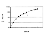
図6は、図5に示した発光輝度を有する各光源8A、8B、・・・、8Xを用いた場合に、出射された光が液晶パネル5に入射されるときの表示画面の各位置に対する各光源8A、8B、・・・、8Xの輝度寄与率を示したものである。横軸は表示画面の、例えば、水平方向における位置、縦軸は各光源8A、8B、・・・、8Xから出射された光の表示輝度に対する輝度寄与率を示している。図6には、例として、領域a〜fに対する輝度寄与率を示す。
6 shows the positions of the display screen when the emitted light is incident on the
図6に示すように、各光源8A、8B、・・・、8Xから出射された光の輝度寄与率は、それぞれ光源8A、8B、・・・、8Xの直前に位置する領域a〜xにおいて最も高く、領域a〜xから離れるに従って徐々に低下する。両端部に配置された光源8A、8Fについては、それぞれ直前に位置する領域a、fにおける輝度寄与率が40%程度とされ、中間の位置に配置された光源8B、8C、8D、8Eについては、それぞれ直前に位置する領域b〜eにおける輝度寄与率が30%程度とされている。また、光源8A、8B、・・・、8Fとも、それぞれ直前に位置する領域a〜f以外の各領域においても表示輝度に寄与して影響を及ぼしている。
As shown in FIG. 6, the luminance contribution ratios of the light emitted from the
このように、表示装置1にあっては、各光源8A、8B、・・・、8Xから出射された光が直前に位置する領域以外の領域にも到達するため、各光源8A、8B、・・・、8Xから出射されたそれぞれの光が、直前に位置する領域a〜xのみに各別に照射されることはなく、他の領域にも照射される。
Thus, in the
表示装置1にあっては、各光源8A、8B、・・・、8Xの発光輝度が領域a〜xの表示輝度に対してどの程度寄与しているのかを予め測定し、この測定値が後述する連立方程式で演算する際のデータとしてメモリ11に記憶されている。従って、メモリ11には、図6に示す輝度寄与率のデータが記憶されている。
In the
次に、図7のフローチャート図を参照して、画面表示に関する制御の処理例について説明する。この制御は、制御部4の液晶パネル制御回路14及び光源制御回路9によって実行され、液晶パネル制御回路14に1フィールドの画像信号が入力されるごとに行われる。
Next, an example of control processing related to screen display will be described with reference to the flowchart of FIG. This control is executed by the liquid crystal
液晶パネル制御回路14に1フィールドの画像信号が入力されると(ステップS1)、入力された画像信号によって生成される1画像(原画像)の表示輝度の分布が液晶パネル制御回路14によって検出される(ステップS2)。このとき各領域a〜xにおける最高表示輝度の高さ及び最高表示輝度を示す位置が検出される。
When an image signal of one field is input to the liquid crystal panel control circuit 14 (step S1), the distribution of display luminance of one image (original image) generated by the input image signal is detected by the liquid crystal
検出した最高表示輝度の高さ及び最高表示輝度を示す位置に基づいて、バックライト3を構成する各光源8A、8B、・・・、8Xの発光輝度がそれぞれ設定される(ステップS3)。この発光輝度の設定時には、領域a〜xの各表示輝度に対する各光源8A、8B、・・・、8Xの発光輝度の輝度寄与率が考慮される。具体的には、メモリ11に予め記憶されている上記輝度寄与率のデータ(図6参照)を用いた連立方程式により、各光源8A、8B、・・・、8Xの発光輝度が設定される。具体的な連立方程式の例については後述する。
Based on the detected maximum display brightness and the position indicating the maximum display brightness, the light emission brightness of each of the
次に、上記のように各光源8A、8B、・・・、8Xの発光輝度を設定した上で、液晶パネル5の表示画面の各部の表示輝度を画像表示の際の最適値にするための各画素に対する補正値を算出する(ステップS4)。
Next, after setting the light emission luminance of each of the
補正値の算出は、設定した各光源8A、8B、・・・、8Xの発光輝度と表示画面の各部における表示輝度の最適値とのずれ量に基づいて行う。最適値とは、入力された画像信号に基づいて原画像が表示されるときに表示画面の各部において必要とされる表示輝度である。従って、補正値は、各光源8A、8B、・・・、8Xから上記のように設定された発光輝度で光が出射されたときに、表示画面の各部において必要とされる表示輝度を得るために各画素において必要とされる開口率を算出するための値である。
The correction value is calculated based on the amount of deviation between the set light emission brightness of each of the
この補正値の算出時には、液晶パネル5の表示ムラを補正するデータをメモリ11から読み出し、このデータを考慮して補正値の算出が行われる。
At the time of calculating the correction value, data for correcting display unevenness of the
ステップS3で設定した各光源8A、8B、・・・、8Xの発光輝度に基づいた発光駆動信号を光源制御回路9から各光源8A、8B、・・・、8Xに送出し、該各光源8A、8B、・・・、8Xを設定した発光輝度で発光させる。同時に、ステップS4で算出した補正値に基づいて補正された表示駆動信号を液晶パネル制御回路14から液晶パネル5の各画素に送出し、各フィールドの画像を表示画面に表示させる(ステップS5)。液晶パネル制御回路14から液晶パネル5の各画素に表示駆動信号が送出されると、各画素が表示駆動信号に基づいた開口率となるように制御され、各光源8A、8B、・・・、8Xから出射された光の各画素に対する透過状態が制御される。
A light emission drive signal based on the light emission luminance of each
従って、表示画面の各部において、入力された画像信号に応じた表示輝度が得られた状態で画像が表示される。 Therefore, an image is displayed in each part of the display screen in a state where display luminance corresponding to the input image signal is obtained.
以下に、上記したステップS1〜ステップS5(図7参照)において行われる制御の具体的な方法について説明する。 Below, the concrete method of the control performed in above-mentioned step S1-step S5 (refer FIG. 7) is demonstrated.
領域a〜xのそれぞれについて、入力される画像信号によって定まる最大表示輝度Ln_max(n=1〜24)を求める。最大表示輝度Ln_maxとは、領域a〜xのそれぞれの各部の中で最大の表示輝度となる値を言う。また、同時に、各領域a〜xのそれぞれについて、最大表示輝度Ln_maxを示す位置を検出する。 For each of the regions a to x, the maximum display luminance Ln_max (n = 1 to 24) determined by the input image signal is obtained. The maximum display brightness Ln_max is a value that provides the maximum display brightness in each part of the regions a to x. At the same time, a position indicating the maximum display luminance Ln_max is detected for each of the regions a to x.
ここで全白の表示輝度(液晶パネル、バックライト共に白ピーク設定(通常、液晶パネルの開口率100%、バックライトの出力100%)の場合)をL_peakとし、表示画面の各領域a〜xについて全白の表示輝度L_peakに対する最大表示輝度Ln_maxの比率αn(n=1〜24)を求める。 Here, the display brightness of all white (when the white peak is set for both the liquid crystal panel and the backlight (usually when the aperture ratio of the liquid crystal panel is 100% and the output of the backlight is 100%)) is L_peak, and each area a to x of the display screen The ratio αn (n = 1 to 24) of the maximum display brightness Ln_max with respect to the display brightness L_peak of all white is obtained.
αn=(Ln_max/L_peak)・・・(1)
比率αnは、領域a〜xに対応する光源8A、8B、・・・、8Xの発光輝度を何割抑制することができるかを示すリカバリー限界である。即ち、液晶パネル5の表示輝度は「液晶パネル(偏光板を含む)の開口率×バックライトの発光輝度」で定まるが、リカバリー限界とは、それ以上バックライトの発光輝度を下げると液晶パネルの開口率を100%に設定しても最大表示輝度Ln_maxが得られなくなる値である。
αn = (Ln_max / L_peak) (1)
The ratio αn is a recovery limit indicating how much the light emission luminance of the
尚、上記には、各領域a〜xの最大表示輝度Ln_maxに基づいてリカバリー限界αnの値を求めるようにしたが、画像内容によっては各領域a〜xの平均表示輝度Ln_aveに基づきαn′=(Ln_ave/L_peak)によりリカバリー限界αn′の値を求めて輝度制御を行うことも可能である。リカバリー限界αn′の値を求めて制御を行う場合には、完全な原画像を再現することは困難であるが、見た目に影響の少ない範囲で原画像を再現することが可能である。 In the above description, the value of the recovery limit αn is obtained based on the maximum display luminance Ln_max of each of the areas a to x. However, depending on the image content, αn ′ = based on the average display luminance Ln_ave of each of the areas a to x. It is also possible to perform luminance control by obtaining the value of the recovery limit αn ′ by (Ln_ave / L_peak). In the case of performing control by obtaining the value of the recovery limit αn ′, it is difficult to reproduce a complete original image, but it is possible to reproduce the original image in a range that does not affect the appearance.
各領域a〜xの表示輝度には、上記したように、それぞれ領域a〜xの直後に位置する光源8A、8B、・・・、8Xの発光輝度以外に他の光源8A、8B、・・・、8Xの発光輝度も寄与するため、各領域a〜xの真後ろに位置する光源8A、8B、・・・、8Xの発光輝度を領域a〜xのリカバリー限界αnに応じて各別に制御するだけでは、領域a〜xの直後に位置しない光源8A、8B、・・・、8Xの発光輝度を考慮した制御を行うことができない。
As described above, the display brightness of each of the regions a to x includes the
そこで、領域a〜xの直後に位置しない光源8A、8B、・・・、8Xの発光輝度をも考慮して光源8A、8B、・・・、8Xごとの発光率βn(n=1〜24)を求める。発光率βnとは、各光源8A、8B、・・・、8Xの最大発光輝度(白ピーク設定時)に対する実際の各光源8A、8B、・・・、8Xの発光輝度の割合を示す値であり、0≦βn≦1の範囲で求められる。例えば、β1は光源8Aの発光率であり、β3は光源8Cの発光率である。
Therefore, considering the light emission luminance of the
発光率βnの算出は、各領域a〜xに対する各光源8A、8B、・・・、8Xの輝度寄与率KX、Y(図6参照)を用いて行う。図6に示した光源8A、8B、・・・、8Xの輝度寄与率のデータは、上記したように、予めメモリ11に記憶されており、発光率βnの算出時にメモリ11に記憶された光源8A、8B、・・・、8Xの輝度寄与率のデータが読み出される。
The light emission rate βn is calculated using the luminance contribution ratios K X and Y (see FIG. 6) of the
輝度寄与率KX、Yにおいて、X、Yとも1〜24の自然数で表され、Xは領域a〜xを示し、Yは光源8A、8B、・・・、8Xを示す。例えば、K1、1は領域aに対する光源8Aの輝度寄与率を示し、K3、7は領域cに対する光源8Gの輝度寄与率を示す。図6に示すように、輝度寄与率は光源8A、8B、・・・、8Xごとに各領域内において一定とされていないが、メモリ11には、輝度寄与率KX、Yとしては、例えば、領域a〜xのそれぞれ中央におけるデータが記憶されている。
In the luminance contribution ratios K X and Y , both X and Y are represented by natural numbers of 1 to 24, X indicates the regions a to x, and Y indicates the
発光率βnは、下記に示す多元連立方程式(不等式)を解くことによって求められる。
K1、1・β1+K1、2・β2+K1、3・β3+・・・+K1、24・β24≧α1
K2、1・β1+K2、2・β2+K2、3・β3+・・・+K2、24・β24≧α2
K3、1・β1+K3、2・β2+K3、3・β3+・・・+K3、24・β24≧α3
・
・
・
K23、1・β1+K23、2・β2+K23、3・β3+・・・+K23、24・β24≧α23
K24、1・β1+K24、2・β2+K24、3・β3+・・・+K24、24・β24≧α24
・・・(2)
尚、上記した多元連立方程式は、バックライトの分割数に応じてnの数が変化するだけであるため、バックライトの構成に拘わらず使用することができる。
The light emission rate βn is obtained by solving the following multiple simultaneous equations (inequality).
K 1,1 · β1 + K 1,2 · β2 +
K 2 , 1 ·
K 3,1 · β1 + K 3,2 , β2 + K 3,3 · β3 + ... + K 3,24 · β24 ≧ α3
・
・
・
K 23 , 1 ·
K 24 , 1 ·
... (2)
The multiple simultaneous equations described above can be used regardless of the configuration of the backlight because the number of n only changes depending on the number of divisions of the backlight.
次に、発光率βn(0≦βn≦1)を補正するが、この補正は、各領域a〜xにおいて隣接する領域とオーバーラップする拡大領域に最大表示輝度Ln_maxを示す位置が存在する場合に、該当する領域について行う。例えば、図8に示すように、領域aにおける最大表示輝度を示す位置Pが領域aの領域b側の端部に存在する場合に、この位置Pは領域bの拡大領域にも存在することになる。領域aに対応して位置された光源8Aは、位置Pが領域aの中央に位置されたと仮定したときの最大表示輝度が得られる発光率β1で発光され発光輝度Mが得られる。このとき、領域bにおける最大表示輝度が領域aにおける最大表示輝度よりも低い場合に、領域aに隣接する領域bに対応して位置された光源8Bについても、光源8Aと同じ発光率β1で発光されるように発光率βを補正して設定する。尚、光源8Aの発光率β1は、上記したように、領域aに対する各光源8B、・・・、8Xの発光輝度の輝度寄与率を考慮して得られた値である。
Next, the light emission rate βn (0 ≦ βn ≦ 1) is corrected. This correction is performed when there is a position indicating the maximum display luminance Ln_max in an enlarged region overlapping with an adjacent region in each of the regions a to x. , For the corresponding area. For example, as shown in FIG. 8, when the position P indicating the maximum display luminance in the area a exists at the end of the area a on the area b side, the position P also exists in the enlarged area of the area b. Become. The
このように拡大領域に最大表示輝度を示す位置が存在する場合には、両領域における最大表示輝度を比較した上で、隣接する領域にそれぞれ対応して位置された光源8、8を高い方の発光率βに合わせる補正を行って発光率βを設定する。
When there is a position showing the maximum display brightness in the enlarged area in this way, the maximum display brightness in both areas is compared, and the
図9は、上記のように発光率βを補正して設定した光源8A、8Bの発光輝度を示したものである。図9に二点差線で示すグラフは光源8A、8Bの発光輝度のトータルの発光輝度を示しており、各領域の外周寄りの部分に最大表示輝度の位置が存在する場合においても、必要とされる発光輝度Mが得られ、外周寄りの部分の最大表示輝度を確保することができる。
FIG. 9 shows the light emission luminance of the
また、最大表示輝度が原領域における外周寄りの部分以外の位置に存在する場合には、その領域の発光率βについて、原領域の中央に対応する発光輝度と拡大領域の境界に対応する発光輝度との比分を上乗せして補正する。例えば、図10に示すように、領域aにおける最大表示輝度を示す位置Pが、原領域a1のうちの拡大領域b2以外の部分に存在するときには、原領域a1の中央Amに対応する発光輝度と拡大領域b2の境界Asに対応する発光輝度との比を算出し、この比分を上乗せして発光率β1を補正する。 In addition, when the maximum display luminance exists at a position other than the portion near the outer periphery in the original region, the emission luminance corresponding to the center of the original region and the emission luminance corresponding to the boundary of the enlarged region with respect to the light emission rate β of the region. Correct by adding the ratio of to. For example, as shown in FIG. 10, when the position P indicating the maximum display luminance in the region a exists in a portion other than the enlarged region b2 in the original region a1, the emission luminance corresponding to the center Am of the original region a1 A ratio with the light emission luminance corresponding to the boundary As of the enlarged region b2 is calculated, and the light emission rate β1 is corrected by adding this ratio.
図11は、上記のように発光率βを補正して設定した光源8Aの発光輝度を示したものである。上乗せ分は図11に斜線で示す部分であり、上乗せ分が、中央Amに対応する発光輝度と隣接する原領域の境界Ap(図10参照)に対応する発光輝度との比分ではなく、中央Amに対応する発光輝度と境界Asに対応する発光輝度との比分に基づくものであるため、小さくて済む。従って、発光輝度の上乗せを最低限に抑えることができ、発光効率の向上を図ることができる。
FIG. 11 shows the light emission luminance of the
上記のように補正した発光率βn(0≦βn≦1)を求めると、この発光率βnを満たすように各光源8A、8B、・・・、8Xの発光輝度を設定する。
When the light emission rate βn (0 ≦ βn ≦ 1) corrected as described above is obtained, the light emission luminances of the
尚、上記には、光源8A、8B、・・・、8Xごとにβnを求める例を示したが、例えば、赤、緑、青の原色ごと又はバックライト3の発光色ごとに、各別にβnを算出して輝度制御を行うことも可能である。
In addition, although the example which calculates | requires (beta) n for every
また、上記にはリカバリー限界αnを算出し、その後、発光率βn(0≦βn≦1)を補正する例を示したが、逆に、リカバリー限界αnを補正した後に発光率βnを多元連立方程式(式(2))を用いて算出するようにしてもよい。 In the above example, the recovery limit αn is calculated, and then the light emission rate βn (0 ≦ βn ≦ 1) is corrected. You may make it calculate using (Formula (2)).
上記のようにして発光率βnを算出し各光源8A、8B、・・・、8Xの発光輝度を設定した後、以下に示すように、液晶パネル5の表示画面の各部の表示輝度を画像表示の際の最適値にするための各画素に対する補正値を算出する。この補正値は、上記したように、各光源8A、8B、・・・、8Xから上記のように設定された発光輝度で光が出射されたときに、表示画面の各部において必要とされる表示輝度を得るために各画素に必要とされる開口率を算出するための値である。
After calculating the light emission rate βn as described above and setting the light emission luminance of each
補正値は、図12に示す液晶パネル5の表示輝度特性についてのデータに基づいて算出する。図12中、横軸はバックライト3の出力を100%としたとき(全点灯時)の液晶パネル5の設定階調(電圧)S_dataを示し、縦軸は設定階調S_dataに対する液晶パネル5の表示輝度L_dataを示す。図12に示す表示輝度特性fのデータは予め求められており、メモリ11に記憶されている。
The correction value is calculated based on data on display luminance characteristics of the
各画素について、全白の表示輝度L_peakと設定表示輝度L_setの比をγとする。設定表示輝度L_setとは、発光率βnに基づいて発光輝度が設定された光源8A、8B、・・・、8Xから光が出射された場合に画素が開口率100%とされたときの表示輝度を言う。
For each pixel, γ is the ratio between the display brightness L_peak of all white and the set display brightness L_set. The set display luminance L_set is the display luminance when the pixel has an aperture ratio of 100% when light is emitted from the
γ = L_peak/L_set・・・(3)
画像信号が入力されたときに表示される画像(原画像)の設定階調S_dataは、上記したように、図12に示すデータにより表示輝度L_dataに基づいて定められる。
γ = L_peak / L_set (3)
As described above, the set gradation S_data of the image (original image) displayed when the image signal is input is determined based on the display luminance L_data by the data shown in FIG.
L_data =f(S_data) ・・・(4)
また、設定表示輝度L_setに対する補正設定階調S_data′は、全白の表示輝度L_peakと設定表示輝度L_setの比γ及び設定階調S_dataに基づいて以下の式によって算出される。補正設定階調S_data′が、各画素において必要とされる開口率を算出するための補正値となる。
L_data = f (S_data) (4)
The corrected set gradation S_data ′ with respect to the set display brightness L_set is calculated by the following expression based on the ratio γ between the display brightness L_peak of all white and the set display brightness L_set and the set gradation S_data. The correction setting gradation S_data ′ is a correction value for calculating the aperture ratio required for each pixel.
S_data′=f(γ×L_data)-1・・・(5)
補正設定階調S_data′となるように各画素の開口率を設定することにより、原画像が所定の表示輝度で再現される。
S_data ′ = f (γ × L_data) −1 (5)
By setting the aperture ratio of each pixel so that the corrected set gradation S_data ′ is obtained, the original image is reproduced with a predetermined display luminance.
表示装置1にあっては、上記した各画素に対する補正量の算出時に、以下のようにして、液晶パネル5の表示ムラを補正する処理が行われる。
In the
液晶パネル5が全白の表示輝度L_peakとされるときには、液晶パネル5において表示ムラが生じる。この表示ムラは液晶パネル5の表示輝度に関与する構成部品、例えば、画素(液晶)や各光源等の成形精度等に起因する。
When the
以下に、表示ムラを防止する方法について説明する(図13及び図14参照)。 Hereinafter, a method of preventing display unevenness will be described (see FIGS. 13 and 14).
図13に示すように、表示画面の各部の表示輝度において、全白の表示輝度L_peakの最小値を均一表示輝度L_flatとする。このとき表示画面の各部において特異的に表示輝度が低い部分がある場合には、その低い表示輝度を無視して均一表示輝度L_flatを設定してもよい。 As shown in FIG. 13, in the display brightness of each part of the display screen, the minimum value of the display brightness L_peak of all white is defined as the uniform display brightness L_flat. At this time, if there is a part where the display brightness is specifically low in each part of the display screen, the uniform display brightness L_flat may be set ignoring the low display brightness.
次に、各画素に対して全白の表示輝度L_peakに対する均一表示輝度L_flatの比H(=L_flat/L_peak)を算出し、この比Hをムラ補正係数としてメモリ11に記憶させる。
Next, the ratio H (= L_flat / L_peak) of the uniform display luminance L_flat with respect to the display luminance L_peak of all white is calculated for each pixel, and this ratio H is stored in the
図14に、図13の表示輝度の状態に対して算出したムラ補正係数Hを示す。 FIG. 14 shows the unevenness correction coefficient H calculated for the display luminance state of FIG.
上記のようにしてムラ補正係数Hを算出し、補正設定階調S_data′をムラ補正係数Hを含めて以下の計算式によって算出することにより、液晶パネル5の表示ムラを防止することができる。
By calculating the unevenness correction coefficient H as described above and calculating the correction setting gradation S_data ′ including the unevenness correction coefficient H by the following calculation formula, display unevenness of the
S_data′=f(H×γ×L_data)-1・・・(6)
以上に記載した通り、表示装置1にあっては、入力した画像信号に応じて、各光源8A、8B、・・・、8Xの発光輝度と液晶パネル5の各画素の開口率を制御しているため、消費電力の低減を図りつつ液晶パネル5に表示される画質の向上を図ることができる。
S_data ′ = f (H × γ × L_data) −1 (6)
As described above, the
また、バックライト3を構成する各光源8A、8B、・・・、8Xの発光輝度を個別に制御しているが、各光源8A、8B、・・・、8Xからそれぞれ出射される光を仕切る構成としていないため、光量制御を行わない従来の液晶表示装置と同様の簡単な構成とすることができる。
Moreover, although the light emission brightness | luminance of each
さらに、表示装置1にあっては、光源8A、8B、・・・、8Xの発光輝度と液晶パネル5の各画素の開口率の制御時に、液晶パネル5が有する表示ムラを補正する処理も行われるため、一層の画質の向上を図ることができる。
Further, the
加えて、表示装置1にあっては、液晶パネル5の表示ムラを補正するデータ、各光源8A、8B、・・・、8Xから出射された光の分布状態についてのデータ、光源8A、8B、・・・、8Xの発光輝度が領域a〜xの表示輝度に対してどの程度寄与しているかを示す輝度寄与率のデータ等の異なる種類のデータが一つのメモリ11に記憶されているため、これらの各データを各別に記憶させる複数のメモリを必要とせず、コストの増大を来たすことなく制御動作を行うことができる。
In addition, in the
次に、光源8A、8B、・・・、8Xの発光輝度の制御量と各画素に対する補正量に関してダイナミックレンジを拡大する制御例について説明する(図15及び図16参照)。
Next, a control example for expanding the dynamic range with respect to the light emission luminance control amount of the
上記には、メモリ11に記憶される表示輝度特性のデータとして図12に示すデータを用いたが、メモリ11に記憶される表示輝度特性のデータとして他のデータを用いることによりダイナミックレンジの拡大が可能である。
In the above, the data shown in FIG. 12 is used as the display luminance characteristic data stored in the
図12に示したデータは、バックライト3が点灯している状態で黒色(黒レベル)を表現する表示輝度特性fを有するデータであるが、例えば、図15に示すように、バックライト3を消灯させた状態で黒レベルを表現する表示輝度特性f′を有するデータを用いることも可能である。このようなデータを用いることにより、光源8A、8B、・・・、8Xの発光輝度の制御量と各画素に対する補正量に関してダイナミックレンジを拡大することができる。
The data shown in FIG. 12 is data having a display luminance characteristic f expressing black (black level) in a state where the
図16のフローチャート図を参照して、光源8A、8B、・・・、8Xの発光輝度の制御量と各画素に対する補正量に関してダイナミックレンジを拡大する際の画面表示に関する制御の処理例について説明する。この制御は、制御部4の液晶パネル制御回路14及び光源制御回路9によって実行され、液晶パネル制御回路14に1フィールドの画像信号が入力されるごとに行われる。
With reference to the flowchart of FIG. 16, an example of control processing related to screen display when the dynamic range is expanded with respect to the control amount of the light emission luminance of the
先ず、ステップS11〜ステップS13の処理を順次行う。ステップS11〜ステップS13の処理は、それぞれ図7に示したステップS1〜ステップ3の処理と同じである。 First, steps S11 to S13 are sequentially performed. The processing of step S11 to step S13 is the same as the processing of step S1 to step 3 shown in FIG.
次に、液晶パネル5の表示画面の各部の表示輝度を画像表示の際の最適値にするための各画素に対する補正値を算出する(ステップS14)。この補正値の算出は、メモリ11に記憶されている図15に示す表示輝度特性f′を有するデータを読み出して行う。補正値の算出を、図15に示す表示輝度特性f′を有するデータを用いて行うことにより、光源8A、8B、・・・、8Xの発光輝度の制御量と各画素に対する補正量に関するダイナミックレンジが拡大される(ステップS15)。
Next, a correction value is calculated for each pixel in order to set the display brightness of each part of the display screen of the
次いで、ステップS14及びステップS15で算出した補正値に基づいて補正された表示駆動信号を液晶パネル制御回路14から液晶パネル5の各画素に送出し、各フィールドの画像を表示画面に表示させる(ステップS16)。液晶パネル制御回路14から液晶パネル5の各画素に表示駆動信号が送出されると、各画素が表示駆動信号に基づいた開口率となるように制御され、各光源8A、8B、・・・、8Xから出射された光の各画素に対する透過状態が制御される。ステップS16の処理は、図7におけるステップ5の処理と同じである。
Next, the display drive signal corrected based on the correction values calculated in step S14 and step S15 is sent from the liquid crystal
上記のように、光源8A、8B、・・・、8Xの発光輝度の制御量と各画素に対する補正量に関するダイナミックレンジを拡大することにより、画質の向上を図ることができる。尚、ダイナミックレンジの拡大処理は、例えば、赤、緑、青の原色ごと又はバックライト3の発光色ごとに行うことも可能である。
As described above, the image quality can be improved by expanding the dynamic range related to the control amount of the light emission luminance of the
次に、表示画面の各領域a〜xについて拡大領域を形成し、この拡大領域を2つの領域に分割した場合の制御例について説明する(図17乃至図21参照)。
尚、拡大領域を分割した場合の制御例は、リカバリー限界αnを補正した後に多元連立方程式(式(2))を用いて発光率βn(0≦βn≦1)を算出するようにしている。従って、以下に示す拡大領域を分割した場合の制御例についての説明にあっては、リカバリー限界αnの補正方法についてのみ詳細に説明する。
Next, an example of control when an enlarged area is formed for each of the areas a to x on the display screen and this enlarged area is divided into two areas will be described (see FIGS. 17 to 21).
In the control example when the enlarged region is divided, the light emission rate βn (0 ≦ βn ≦ 1) is calculated using the multiple simultaneous equations (formula (2)) after correcting the recovery limit αn. Therefore, in the following description of the control example when the enlarged region is divided, only the method for correcting the recovery limit αn will be described in detail.
各領域a〜xは、図17に示すように、表示画面が等分に分割されて形成された原領域12(右上がりの斜線部分)と該原領域12の外側に位置する第1の拡大領域13(左上がりの斜線部分)と該第1の拡大領域13の外側に位置する第2の拡大領域14(梨地の部分)とによって構成されている。図17中、点線で区切った領域が原領域12を示し、二点鎖線で区切った領域のうち原領域12を除いた領域が第1の拡大領域13を示し、実線で区切った領域のうち原領域12及び第1の拡大領域13を除いた領域が第2の拡大領域14を示す。
As shown in FIG. 17, each of the areas a to x includes an original area 12 (a portion with a diagonal line rising to the right) formed by dividing the display screen into equal parts, and a first enlargement located outside the
リカバリー限界αnの補正は、各領域a〜xにおける最大表示輝度Ln_maxを示す位置に応じて行う。 The recovery limit αn is corrected according to the position indicating the maximum display luminance Ln_max in each of the areas a to x.
例えば、分割領域a〜xの原領域12の最大表示輝度が図18に示すような状態であったとする。図18中、ポイントマークは各領域a〜xの原領域12における最大表示輝度の位置を示し、数値は最大表示輝度の高さを示す。最大表示輝度は数値が小さいほど高いものとする。
For example, it is assumed that the maximum display brightness of the
図19は、図18の最大表示輝度の状態等をまとめて示す図表である。図19中、左側から「領域」は各領域a〜xを示し、「原領域」は各領域a〜xの原領域12における最大表示輝度の高さを示し、「第1の拡大領域」は各領域a〜xを第1の拡大領域13まで拡大したときの最大表示輝度の高さを示し、「第2の拡大領域」は各領域a〜xを第2の拡大領域14まで拡大したときの最大表示輝度の高さを示す。
FIG. 19 is a chart collectively showing the state of the maximum display luminance and the like shown in FIG. In FIG. 19, “region” from the left side indicates each region a to x, “original region” indicates the height of the maximum display brightness in the
例えば、領域iについては、原領域12における最大表示輝度が「1」であり、第1の拡大領域13まで拡大したときの最大表示輝度も「1」である。第2の拡大領域14まで拡大したときには領域jの最大表示輝度「22」が含まれるが、最大表示輝度「1」の方が最大表示輝度「22」より高いため、第2の拡大領域14まで拡大したときも最大表示輝度は「1」となる。また、領域rについては、原領域12における最大表示輝度が「24」であり、第1の拡大領域13まで拡大したときの最大表示輝度も「24」である。第2の拡大領域14まで拡大したときには領域lの最大表示輝度「20」が含まれ、最大表示輝度「20」の方が最大表示輝度「24」より高いため、第2の拡大領域14まで拡大したときの最大表示輝度は「20」となる。
For example, for the area i, the maximum display brightness in the
図19中、「等価領域」は、各領域a〜xを何れの領域と同じに見るかを示し、「位置」は、各領域a〜xの原領域12における最大表示輝度の位置が、以下に示すA〜Dの何れのエリアに属するかを示したものである。
In FIG. 19, “equivalent area” indicates which area a to x is viewed as the same as, and “position” indicates the position of the maximum display luminance in the
A〜Dのエリアは、図20に示すように定められており、各領域a〜xにおいて、原領域12のうち最も外周側のエリアがエリアAとされ、エリアAの内側のエリアがエリアBとされ、エリアBの内側の矩形状のエリアがエリアC又はエリアDとされる。エリアAは隣接する領域における第1の拡大領域13に相当するエリアであり、エリアBは隣接する領域における第2の拡大領域14に相当するエリアであり、エリアC、Dは隣接する領域における第1の拡大領域13にも第2の拡大領域14にも相当しないエリアである。
The areas A to D are determined as shown in FIG. 20. In each of the areas a to x, the outermost area of the
「位置」がエリアAに決定された領域においては、リカバリー限界αを該当する「等価領域」におけるリカバリー限界αと同じ設定にする処理が行われる。「位置」がエリアBに決定された領域においては、その領域におけるリカバリー限界αをP倍に設定する処理が行われる。「位置」がエリアCに決定された領域においては、その領域におけるリカバリー限界αをQ(Q<P)倍に設定する処理が行われる。「位置」がエリアDに決定された領域においては、特に処理が行われず、リカバリー限界αが変更されない。 In the area where the “position” is determined as the area A, the recovery limit α is set to the same setting as the recovery limit α in the corresponding “equivalent area”. In an area where “position” is determined as area B, processing for setting the recovery limit α in that area to P times is performed. In the area where the “position” is determined as the area C, a process for setting the recovery limit α in the area to Q (Q <P) times is performed. In the area where the “position” is determined as the area D, no particular processing is performed, and the recovery limit α is not changed.
エリアBに決定された領域におけるPの値は、例えば、1.3であり、エリアCに決定された領域におけるQの値は、例えば、1.03である。P、Qはともに図11に示した上乗せ分であり、P、Qは原領域12の中央に対応する発光輝度と第1の拡大領域13又は第2の拡大領域14の境界に対応する発光輝度との比分に応じて任意の値に設定することができる。
The value of P in the area determined as the area B is 1.3, for example, and the value of Q in the area determined as the area C is, for example, 1.03. P and Q are the additions shown in FIG. 11, and P and Q are the emission luminance corresponding to the center of the
以下に、各領域a〜xがA〜Dのエリアの何れのエリアに決定されるかに関する処理の手順について説明する(図21参照)。尚、以下の手順においては、図19及び図20に示した具体例に基づいて各領域a〜xが何れのエリアに決定されるかを併せて説明する。 Hereinafter, a procedure of processing relating to which of the areas A to D is determined for each of the areas a to x will be described (see FIG. 21). In the following procedure, it will be described together with which area each of the regions a to x is determined based on the specific examples shown in FIGS. 19 and 20.
(S1)処理が開始され、第1の拡大領域13に、原領域12における最大表示輝度より高い隣接する他の領域における最大表示輝度が存在するか否かが検出される。存在することが検出された場合には(S2)に移行し、存在することが検出されなかった場合には(S3)に移行する。具体的には、領域b、j、k、p、u、xが(S2)に移行し、他の領域a、c、d、e、f、g、h、i、l、m、n、o、q、r、s、t、v、wが(S3)に移行する。存在することが検出された領域b、j、k、p、u、xは「等価領域」がそれぞれ他の領域に該当するa、d、e、v、t、wに確定される。
(S1) The process is started, and it is detected whether or not the
(S2)(S1)において存在することが検出された領域及び該領域に対して(S1)において他の領域に該当する領域がエリアAに決定される。具体的には、(S1)において存在することが検出された領域b、j、k、p、u、xと(S1)において他の領域に該当する領域a、d、e、t、v、wがエリアAに決定される。該当する領域がエリアAに決定されることにより、処理を終了する。 (S2) The area corresponding to the other area is determined as area A in (S1) with respect to the area detected to exist in (S1). Specifically, the regions b, j, k, p, u, x detected to exist in (S1) and the regions a, d, e, t, v, corresponding to other regions in (S1). w is determined as area A. When the corresponding area is determined as area A, the process is terminated.
(S3)第2の拡大領域14に、原領域12における最大表示輝度より高い隣接する他の領域における最大表示輝度が存在するか否かが検出される。存在することが検出された場合には(S4)に移行し、存在することが検出されなかった場合には(S9)に移行する。具体的には、領域c、e、g、n、r、s、wが(S4)に移行し、領域a、d、f、h、i、l、m、o、q、t、vが(S9)に移行する。
(S3) It is detected whether or not the
(S4)既にエリアAに決定されているか否かが検出される。決定されていることが検出された場合には(S4′)に移行し、決定されていることが検出されなかった場合には(S6)に移行する。具体的には、(S2)においてエリアAに決定された領域e、wが(S4′)に移行し、領域c、g、n、r、sが(S6)に移行する。 (S4) Whether or not the area A has already been determined is detected. If it is detected that it has been determined, the process proceeds to (S4 ′), and if it is not detected that it has been determined, the process proceeds to (S6). Specifically, the areas e and w determined as the area A in (S2) shift to (S4 ′), and the areas c, g, n, r, and s shift to (S6).
(S4′)(S4)において存在することが検出された領域に対して他の領域に該当する領域が既にエリアAに決定されているか否かが検出される。決定されていることが検出された場合には(S5)に移行し、決定されていることが検出されなかった場合には(S5′)に移行する。具体的には、他の領域に該当する領域dが(S2)において既にエリアAに決定された領域eが(S5)に移行し、他の領域に該当する領域qがエリアAに決定されていない領域wが(S5′)に移行する。 (S4 ′) It is detected whether or not an area corresponding to another area is already determined as area A with respect to the area detected to exist in (S4). If it is detected that it is determined, the process proceeds to (S5), and if it is not detected that it is determined, the process proceeds to (S5 '). Specifically, the area e that has already been determined to be the area A in (S2) has shifted to (S5), and the area q that corresponds to the other area has been determined to be the area A. The area w that does not exist shifts to (S5 ′).
(S5)既にエリアAに決定されているため、特に処理は行われず、処理を終了する。具体的には、領域eはエリアAのままである。 (S5) Since the area A has already been determined, no particular process is performed and the process is terminated. Specifically, the area e remains the area A.
(S5′)他の領域に該当する領域がエリアBに決定される。具体的には、領域wの他の領域に該当する領域qがエリアBに決定される。 (S5 ′) An area corresponding to another area is determined as area B. Specifically, a region q corresponding to another region w is determined as area B.
(S6)(S3)において存在することが検出された領域に対して他の領域に該当する領域が既にエリアAに決定されているか否かが検出される。決定されていることが検出された場合には(S8)に移行し、決定されていることが検出されなかった場合には(S7)に移行する。具体的には、領域c、nが(S8)に移行し、領域g、r、sが(S7)に移行する。 (S6) It is detected whether or not an area corresponding to another area is already determined as area A with respect to the area detected to exist in (S3). If it is detected that it is determined, the process proceeds to (S8), and if it is not detected that it is determined, the process proceeds to (S7). Specifically, the regions c and n shift to (S8), and the regions g, r, and s shift to (S7).
(S7)(S6)において決定されていることが検出されなかった領域がエリアDに決定され、(S6)において他の領域に該当した領域がエリアBに決定される。具体的には、領域g、r、sがエリアDに決定され、領域h、l、nがエリアBに決定され、処理を終了する。 (S7) A region that is not detected to be determined in (S6) is determined as area D, and a region corresponding to another region is determined as area B in (S6). Specifically, the areas g, r, and s are determined as the area D, the areas h, l, and n are determined as the area B, and the process ends.
(S8)(S6)において決定されていることが検出された領域cがエリアDに決定される。領域nも(S6)において決定されていることが検出された領域であるが、(S7)において既にエリアBに決定されているため、領域nはエリアBのままとなり、処理を終了する。 (S8) The area c detected to be determined in (S6) is determined as the area D. The area n is also an area that has been determined to have been determined in (S6), but since it has already been determined to be area B in (S7), area n remains area B and the process ends.
(S9)既にエリアA又はエリアBに決定されているか否かが検出される。決定されていることが検出された場合には(S10)に移行し、決定されていることが検出されなかった場合には(S11)に移行する。具体的には、(S2)においてエリアAに決定された領域a、d、t、v、(S7)においてエリアBに決定された領域h、l及び(S5′)においてエリアBに決定された領域qが(S10)に移行し、領域f、i、m、oが(S11)に移行する。 (S9) Whether the area A or the area B has already been determined is detected. If it is detected that it is determined, the process proceeds to (S10), and if it is not detected that it is determined, the process proceeds to (S11). Specifically, the areas a, d, t, v determined in area A in (S2), the areas h, l determined in area B in (S7), and the area B in (S5 ′). The region q shifts to (S10), and the regions f, i, m, and o shift to (S11).
(S10)既にエリアA又はエリアBに決定されているため、特に処理は行われず、処理を終了する。具体的には、領域a、d、t、vはエリアAのままであり、領域h、l、qはエリアBのままである。 (S10) Since the area A or the area B has already been determined, the process is not performed and the process ends. Specifically, the areas a, d, t, and v remain in the area A, and the areas h, l, and q remain in the area B.
(S11)(S9)において決定されていることが検出されなかった領域f、i、m、oがエリアCに決定されて処理を終了する。 (S11) Regions f, i, m, and o that are not detected to be determined in (S9) are determined as area C, and the process ends.
以上のようにして各領域a〜xのエリアが決定されると、エリアAに決定された領域におけるリカバリー限界αは対応する等価領域におけるリカバリー限界αと同一に設定され、エリアBに決定された領域におけるリカバリー限界αはP倍に設定され、エリアCに決定された領域におけるリカバリー限界αはQ倍に設定され、エリアDに決定された領域におけるリカバリー限界αは変更されずに設定される。 When the areas a to x are determined as described above, the recovery limit α in the area determined as the area A is set to be the same as the recovery limit α in the corresponding equivalent area and is determined as the area B. The recovery limit α in the area is set to P times, the recovery limit α in the area determined for the area C is set to Q times, and the recovery limit α in the area determined for the area D is set unchanged.
上記のようにして設定されたリカバリー限界αに基づいて、多元連立方程式(式(2))を用いて発光率βn(0≦βn≦1)を算出する。 Based on the recovery limit α set as described above, the light emission rate βn (0 ≦ βn ≦ 1) is calculated using the multiple simultaneous equations (formula (2)).
尚、上記には、表示画面の領域の分割数を24個に設定した例を示したが、領域の分割数は24個に限られることはなく任意である。 In the above example, the number of divisions of the display screen area is set to 24. However, the number of divisions of the area is not limited to 24 and is arbitrary.
また、上記には、拡大領域を一つ又は二つに設定した例を示したが、拡大領域の数も任意に設定することが可能である。 Moreover, although the example which set the expansion area to one or two was shown above, the number of expansion areas can also be set arbitrarily.
上記した最良の形態において示した各部の具体的な形状及び構造は、何れも本発明を実施する際の具体化のほんの一例を示したものにすぎず、これらによって本発明の技術的範囲が限定的に解釈されることがあってはならないものである。 The specific shapes and structures of the respective parts shown in the above-described best mode are merely examples of the implementation of the present invention, and the technical scope of the present invention is limited by these. It should not be interpreted in a general way.
1…液晶表示装置、2…表示部、3…バックライト、4…制御部、8A〜8X…光源、13…第1の拡大領域、14…第2の拡大領域
DESCRIPTION OF
Claims (6)
該表示部の背面を照明すると共に表示部の複数の分割領域に対応して各別に配置された複数の光源によって構成されたバックライトと、
入力された画像信号に基づいて表示画面に画像が表示されるときに表示部の各分割領域における表示輝度を検出し、各分割領域に対応して配置された各光源の発光輝度を、隣接する分割領域に対応して配置された他の光源の当該領域に対する影響を含め各分割領域において最大の表示輝度を示す位置に応じて算出し、各分割領域に対応して配置された各光源の発光輝度をそれぞれ上記算出した発光輝度に設定し、設定した発光輝度と表示画面の各部における表示輝度の最適値とのずれ量に基づいて表示部の各画素に対する補正量を算出し、算出した補正量に基づいて生成した表示駆動信号を各画素に対して送出し各画素の開口率を制御する制御部とを備えた
ことを特徴とする表示装置。 Each divided area has a display screen divided into a plurality of areas, is controlled in pixel units and has an aperture ratio, and each divided area is provided with an enlarged area that overlaps with the adjacent divided areas. The display area is set including the enlarged area,
A backlight configured to illuminate the back surface of the display unit and includes a plurality of light sources arranged separately corresponding to the plurality of divided regions of the display unit;
When an image is displayed on the display screen based on the input image signal, the display brightness in each divided area of the display unit is detected, and the light emission brightness of each light source arranged corresponding to each divided area is adjacent. The light emission of each light source arranged corresponding to each divided area is calculated according to the position showing the maximum display luminance in each divided area including the influence of the other light sources arranged corresponding to the divided areas on the corresponding area. The brightness is set to the calculated light emission brightness, the correction amount for each pixel of the display unit is calculated based on the amount of deviation between the set light emission brightness and the optimum value of the display brightness in each part of the display screen, and the calculated correction amount And a control unit that controls the aperture ratio of each pixel by sending a display drive signal generated based on the above to each pixel.
複数に分割された各領域に前記最大の表示輝度を示す位置が存在するときに、前記各領域に応じた発光輝度を算出した
ことを特徴とする請求項1に記載の表示装置。 Divide the enlarged area in each divided area into multiple areas ,
2. The display device according to claim 1 , wherein when a position indicating the maximum display brightness exists in each of the plurality of divided areas, the light emission brightness corresponding to each of the areas is calculated .
ことを特徴とする請求項1に記載の表示装置。 The above calculation of the light emission luminance of each light source including the influence of other light sources on the region is performed by simultaneous equations using the luminance contribution ratio in which the light emission luminances of all light sources contribute to the region. The display device according to claim 1.
ことを特徴とする請求項1に記載の表示装置。 The controller controls the dynamic range of display luminance in each divided area of the display unit when an image signal is input from the state where the light emission luminance of each light source arranged corresponding to each divided area is substantially zero. The display device according to claim 1, wherein the display brightness in each divided area of the display unit is detected by assigning the display state up to the state of the display unit.
表示部の各分割領域に、隣接する分割領域との間で互いにオーバーラップする拡大領域を設けて各分割領域の領域範囲を拡大領域を含めて設定し、
制御部によって、
入力された画像信号に基づいて表示画面に画像が表示されるときに表示部の各分割領域における表示輝度を検出し、
各分割領域に対応して配置された各光源の発光輝度を、隣接する分割領域に対応して配置された他の光源の当該領域に対する影響を含め各分割領域において最大の表示輝度を示す位置に応じて算出し、
各分割領域に対応して配置された各光源の発光輝度をそれぞれ上記算出した発光輝度に設定し、
設定した発光輝度と表示画面の各部における表示輝度の最適値とのずれ量に基づいて表示部の各画素に対する補正量を算出し、
算出した補正量に基づいて生成した表示駆動信号を各画素に対して送出し各画素の開口率を制御するようにした
ことを特徴とする表示方法。 A display unit having a display screen divided into a plurality of areas and controlled in pixel units to set an aperture ratio, and the back surface of the display unit is illuminated and arranged separately for each of the plurality of areas of the display unit An image display method in a display device including a backlight configured by a plurality of light sources,
In each divided area of the display unit, an enlarged area that overlaps with the adjacent divided areas is provided, and the area range of each divided area is set including the enlarged area,
By controller
When the image is displayed on the display screen based on the input image signal, the display brightness in each divided area of the display unit is detected,
The light emission luminance of each light source arranged corresponding to each divided region is set to a position showing the maximum display luminance in each divided region including the influence of the other light sources arranged corresponding to the adjacent divided regions on the relevant region. Calculate accordingly,
Set the emission luminance of each light source arranged corresponding to each divided area to the calculated emission luminance,
Calculate the correction amount for each pixel of the display unit based on the amount of deviation between the set emission luminance and the optimum value of the display luminance in each part of the display screen,
A display method, wherein a display drive signal generated based on the calculated correction amount is sent to each pixel to control an aperture ratio of each pixel.
ことを特徴とする請求項5に記載の表示方法。 The display method according to claim 5, wherein the control unit performs a process of correcting display unevenness of the display unit when calculating a correction amount for each pixel of the display unit.
Priority Applications (1)
| Application Number | Priority Date | Filing Date | Title |
|---|---|---|---|
| JP2006002677A JP4951973B2 (en) | 2006-01-10 | 2006-01-10 | Display device and display method |
Applications Claiming Priority (1)
| Application Number | Priority Date | Filing Date | Title |
|---|---|---|---|
| JP2006002677A JP4951973B2 (en) | 2006-01-10 | 2006-01-10 | Display device and display method |
Publications (2)
| Publication Number | Publication Date |
|---|---|
| JP2007183499A JP2007183499A (en) | 2007-07-19 |
| JP4951973B2 true JP4951973B2 (en) | 2012-06-13 |
Family
ID=38339651
Family Applications (1)
| Application Number | Title | Priority Date | Filing Date |
|---|---|---|---|
| JP2006002677A Expired - Fee Related JP4951973B2 (en) | 2006-01-10 | 2006-01-10 | Display device and display method |
Country Status (1)
| Country | Link |
|---|---|
| JP (1) | JP4951973B2 (en) |
Families Citing this family (30)
| Publication number | Priority date | Publication date | Assignee | Title |
|---|---|---|---|---|
| US8139022B2 (en) | 2007-05-08 | 2012-03-20 | Victor Company Of Japan, Limited | Liquid crystal display device and image display method thereof |
| KR101450143B1 (en) * | 2007-10-25 | 2014-10-14 | 삼성디스플레이 주식회사 | Timing controller, liquid crystal display comprising the same and driving method of liquid crystal display |
| KR101320018B1 (en) * | 2007-12-04 | 2013-10-18 | 삼성디스플레이 주식회사 | Light source and driving method the same and display device having the same |
| JP4840393B2 (en) * | 2008-04-11 | 2011-12-21 | ソニー株式会社 | Display control apparatus and method, and program |
| JP5217586B2 (en) * | 2008-04-11 | 2013-06-19 | ソニー株式会社 | Display control apparatus and method, and program |
| JP2010044180A (en) * | 2008-08-12 | 2010-02-25 | Victor Co Of Japan Ltd | Liquid crystal display device and video signal processing method used for the same |
| KR100959594B1 (en) * | 2008-05-01 | 2010-05-27 | 닛뽕빅터 가부시키가이샤 | Liquid crystal display apparatus and image display method used therefor |
| US8159451B2 (en) | 2008-05-26 | 2012-04-17 | Kabushiki Kaisha Toshiba | Light-emission control device and liquid crystal display apparatus |
| KR100950682B1 (en) * | 2008-07-24 | 2010-03-31 | 전자부품연구원 | Apparatus and method for compensating brightness of back light |
| KR101511130B1 (en) * | 2008-07-25 | 2015-04-13 | 삼성디스플레이 주식회사 | Method for boosting a display image, controller unit for performing the method, and display apparatus having the controller unit |
| KR101512047B1 (en) * | 2008-08-13 | 2015-04-16 | 삼성디스플레이 주식회사 | Local driving method of light source light-source apparatus performing for the method and display apparatus having the light-source apparatus |
| BRPI0922632A2 (en) * | 2008-12-01 | 2016-01-05 | Sharp Kk | backlight unit, liquid crystal display device, data generation method, data generation program and computer readable recording medium |
| KR101605157B1 (en) * | 2009-03-24 | 2016-03-22 | 삼성디스플레이 주식회사 | Method for driving display apparatus |
| CN101983400B (en) | 2009-05-15 | 2013-07-17 | 株式会社东芝 | Image display device |
| JP4892036B2 (en) * | 2009-06-08 | 2012-03-07 | 株式会社東芝 | Liquid crystal display device and video processing device |
| JP2011013458A (en) * | 2009-07-02 | 2011-01-20 | Panasonic Corp | Liquid crystal display device |
| JP2011017910A (en) * | 2009-07-09 | 2011-01-27 | Panasonic Corp | Liquid crystal display device |
| JP5516583B2 (en) * | 2009-07-16 | 2014-06-11 | 富士通株式会社 | Display device and control method |
| WO2011010380A1 (en) | 2009-07-23 | 2011-01-27 | 富士通株式会社 | Display device and control method |
| BR112012001784A2 (en) | 2009-07-30 | 2019-09-24 | Sharp Kk | "image display device and image display method" |
| JP2011033978A (en) * | 2009-08-05 | 2011-02-17 | Sharp Corp | Liquid crystal image display device and display control method thereof |
| KR101067631B1 (en) * | 2009-10-13 | 2011-09-26 | 주식회사 티엘아이 | Local Dimming type LCD for producing Driving voltage having the level responding the illuminance of neigboring back light block |
| KR101053158B1 (en) * | 2009-10-13 | 2011-08-02 | 주식회사 티엘아이 | Local dimming liquid crystal display that generates an image that reflects input data more effectively |
| KR101128145B1 (en) * | 2009-10-26 | 2012-03-23 | 엘지전자 주식회사 | method for driving the backlight unit and display apparatus thereof |
| KR101006050B1 (en) * | 2010-09-06 | 2011-01-07 | (주)원테크놀로지 | The correction process of led electric sign |
| CN103354935B (en) | 2011-02-09 | 2015-04-01 | 三菱电机株式会社 | Light-emission control device, light-emission control method, light emitting device, image display device |
| WO2013121707A1 (en) * | 2012-02-13 | 2013-08-22 | パナソニック株式会社 | Display device and display method |
| CN103559862B (en) * | 2013-11-11 | 2016-08-17 | 西安诺瓦电子科技有限公司 | The Subarea calibration method of LED display |
| CN115167046B (en) * | 2020-03-31 | 2023-11-10 | 厦门天马微电子有限公司 | Display panel and display device |
| WO2023108550A1 (en) * | 2021-12-16 | 2023-06-22 | Jade Bird Display (Shanghai) Company | System for detecting pixel defect |
Family Cites Families (6)
| Publication number | Priority date | Publication date | Assignee | Title |
|---|---|---|---|---|
| JP3523170B2 (en) * | 2000-09-21 | 2004-04-26 | 株式会社東芝 | Display device |
| JP2004317895A (en) * | 2003-04-18 | 2004-11-11 | Hitachi Lighting Ltd | Signal processing method for image information and image information display device |
| JP4628770B2 (en) * | 2004-02-09 | 2011-02-09 | 株式会社日立製作所 | Image display device having illumination device and image display method |
| JP2005241678A (en) * | 2004-02-24 | 2005-09-08 | Matsushita Electric Ind Co Ltd | Liquid crystal display apparatus |
| JP2005309338A (en) * | 2004-04-26 | 2005-11-04 | Mitsubishi Electric Corp | Apparatus and method for image display |
| KR100619627B1 (en) * | 2004-05-27 | 2006-09-08 | 엘지.필립스 엘시디 주식회사 | Apparatus and method for luminance control of liquid crystal display device |
-
2006
- 2006-01-10 JP JP2006002677A patent/JP4951973B2/en not_active Expired - Fee Related
Also Published As
| Publication number | Publication date |
|---|---|
| JP2007183499A (en) | 2007-07-19 |
Similar Documents
| Publication | Publication Date | Title |
|---|---|---|
| JP4951973B2 (en) | Display device and display method | |
| JP4904783B2 (en) | Display device and display method | |
| JP4818351B2 (en) | Image processing apparatus and image display apparatus | |
| JP5114872B2 (en) | Display control device, display device, and display control method | |
| KR101405155B1 (en) | Display device and display control method | |
| JP5122927B2 (en) | Image display device and image display method | |
| JP5887045B2 (en) | Display image boosting method, controller unit for performing the same, and display device having the same | |
| JP5734580B2 (en) | Pixel data correction method and display device for performing the same | |
| JP2007322882A (en) | Display device and display control method | |
| JP6777485B2 (en) | Image display device and image display method | |
| KR100753318B1 (en) | Display device | |
| KR20220059684A (en) | Apparatus and method for driving display panel, and display device | |
| JP4894358B2 (en) | Backlight drive device, display device, and backlight drive method | |
| WO2011129124A1 (en) | Display device | |
| US20110285611A1 (en) | Liquid crystal display | |
| US11948522B2 (en) | Display device with light adjustment for divided areas using an adjustment coefficient | |
| JP4888695B2 (en) | Display device and display method | |
| US9123303B2 (en) | Display device, display method, and program | |
| US20140327708A1 (en) | Display device | |
| JP2018116256A (en) | Display device and display method | |
| JP2018194567A (en) | Light-emitting device, display device and method for controlling light-emitting device | |
| WO2012141114A1 (en) | Image display device and image display method | |
| JP2019179187A (en) | Image display device and control method thereof | |
| WO2018131357A1 (en) | Display device and display method | |
| JP2021033045A (en) | Liquid crystal display device and control method therefor |
Legal Events
| Date | Code | Title | Description |
|---|---|---|---|
| A621 | Written request for application examination |
Free format text: JAPANESE INTERMEDIATE CODE: A621 Effective date: 20081208 |
|
| A977 | Report on retrieval |
Free format text: JAPANESE INTERMEDIATE CODE: A971007 Effective date: 20111124 |
|
| A131 | Notification of reasons for refusal |
Free format text: JAPANESE INTERMEDIATE CODE: A131 Effective date: 20111201 |
|
| A521 | Written amendment |
Free format text: JAPANESE INTERMEDIATE CODE: A523 Effective date: 20120125 |
|
| TRDD | Decision of grant or rejection written | ||
| A01 | Written decision to grant a patent or to grant a registration (utility model) |
Free format text: JAPANESE INTERMEDIATE CODE: A01 Effective date: 20120214 |
|
| A01 | Written decision to grant a patent or to grant a registration (utility model) |
Free format text: JAPANESE INTERMEDIATE CODE: A01 |
|
| A61 | First payment of annual fees (during grant procedure) |
Free format text: JAPANESE INTERMEDIATE CODE: A61 Effective date: 20120227 |
|
| FPAY | Renewal fee payment (event date is renewal date of database) |
Free format text: PAYMENT UNTIL: 20150323 Year of fee payment: 3 |
|
| LAPS | Cancellation because of no payment of annual fees |