JP4941332B2 - Imaging device - Google Patents
Imaging device Download PDFInfo
- Publication number
- JP4941332B2 JP4941332B2 JP2008016716A JP2008016716A JP4941332B2 JP 4941332 B2 JP4941332 B2 JP 4941332B2 JP 2008016716 A JP2008016716 A JP 2008016716A JP 2008016716 A JP2008016716 A JP 2008016716A JP 4941332 B2 JP4941332 B2 JP 4941332B2
- Authority
- JP
- Japan
- Prior art keywords
- imaging
- image
- microlens
- data
- unit
- Prior art date
- Legal status (The legal status is an assumption and is not a legal conclusion. Google has not performed a legal analysis and makes no representation as to the accuracy of the status listed.)
- Expired - Fee Related
Links
- 238000003384 imaging method Methods 0.000 title claims description 201
- 238000000034 method Methods 0.000 description 31
- 230000008569 process Effects 0.000 description 25
- 230000008707 rearrangement Effects 0.000 description 21
- 230000007547 defect Effects 0.000 description 8
- 230000000052 comparative effect Effects 0.000 description 6
- 230000009467 reduction Effects 0.000 description 5
- 230000000295 complement effect Effects 0.000 description 3
- 238000010586 diagram Methods 0.000 description 3
- 230000003287 optical effect Effects 0.000 description 3
- 239000003086 colorant Substances 0.000 description 2
- 230000000694 effects Effects 0.000 description 2
- 239000011159 matrix material Substances 0.000 description 2
- 230000035945 sensitivity Effects 0.000 description 2
- 230000005856 abnormality Effects 0.000 description 1
- 230000009471 action Effects 0.000 description 1
- 238000003491 array Methods 0.000 description 1
- 238000010276 construction Methods 0.000 description 1
- 238000005286 illumination Methods 0.000 description 1
- 239000007788 liquid Substances 0.000 description 1
- 239000004973 liquid crystal related substance Substances 0.000 description 1
- 229910044991 metal oxide Inorganic materials 0.000 description 1
- 150000004706 metal oxides Chemical class 0.000 description 1
- 238000012986 modification Methods 0.000 description 1
- 230000004048 modification Effects 0.000 description 1
- 239000004065 semiconductor Substances 0.000 description 1
- 239000007787 solid Substances 0.000 description 1
- 230000003595 spectral effect Effects 0.000 description 1
- 230000000007 visual effect Effects 0.000 description 1
Images


Classifications
-
- H—ELECTRICITY
- H01—ELECTRIC ELEMENTS
- H01L—SEMICONDUCTOR DEVICES NOT COVERED BY CLASS H10
- H01L27/00—Devices consisting of a plurality of semiconductor or other solid-state components formed in or on a common substrate
- H01L27/14—Devices consisting of a plurality of semiconductor or other solid-state components formed in or on a common substrate including semiconductor components sensitive to infrared radiation, light, electromagnetic radiation of shorter wavelength or corpuscular radiation and specially adapted either for the conversion of the energy of such radiation into electrical energy or for the control of electrical energy by such radiation
- H01L27/144—Devices controlled by radiation
- H01L27/146—Imager structures
- H01L27/14601—Structural or functional details thereof
- H01L27/14625—Optical elements or arrangements associated with the device
- H01L27/14627—Microlenses
-
- H—ELECTRICITY
- H04—ELECTRIC COMMUNICATION TECHNIQUE
- H04N—PICTORIAL COMMUNICATION, e.g. TELEVISION
- H04N23/00—Cameras or camera modules comprising electronic image sensors; Control thereof
- H04N23/80—Camera processing pipelines; Components thereof
-
- H—ELECTRICITY
- H04—ELECTRIC COMMUNICATION TECHNIQUE
- H04N—PICTORIAL COMMUNICATION, e.g. TELEVISION
- H04N23/00—Cameras or camera modules comprising electronic image sensors; Control thereof
- H04N23/80—Camera processing pipelines; Components thereof
- H04N23/84—Camera processing pipelines; Components thereof for processing colour signals
- H04N23/843—Demosaicing, e.g. interpolating colour pixel values
-
- H—ELECTRICITY
- H04—ELECTRIC COMMUNICATION TECHNIQUE
- H04N—PICTORIAL COMMUNICATION, e.g. TELEVISION
- H04N25/00—Circuitry of solid-state image sensors [SSIS]; Control thereof
- H04N25/10—Circuitry of solid-state image sensors [SSIS]; Control thereof for transforming different wavelengths into image signals
- H04N25/11—Arrangement of colour filter arrays [CFA]; Filter mosaics
- H04N25/13—Arrangement of colour filter arrays [CFA]; Filter mosaics characterised by the spectral characteristics of the filter elements
- H04N25/134—Arrangement of colour filter arrays [CFA]; Filter mosaics characterised by the spectral characteristics of the filter elements based on three different wavelength filter elements
-
- H—ELECTRICITY
- H01—ELECTRIC ELEMENTS
- H01L—SEMICONDUCTOR DEVICES NOT COVERED BY CLASS H10
- H01L27/00—Devices consisting of a plurality of semiconductor or other solid-state components formed in or on a common substrate
- H01L27/14—Devices consisting of a plurality of semiconductor or other solid-state components formed in or on a common substrate including semiconductor components sensitive to infrared radiation, light, electromagnetic radiation of shorter wavelength or corpuscular radiation and specially adapted either for the conversion of the energy of such radiation into electrical energy or for the control of electrical energy by such radiation
- H01L27/144—Devices controlled by radiation
- H01L27/146—Imager structures
- H01L27/14601—Structural or functional details thereof
- H01L27/1462—Coatings
- H01L27/14623—Optical shielding
-
- H—ELECTRICITY
- H04—ELECTRIC COMMUNICATION TECHNIQUE
- H04N—PICTORIAL COMMUNICATION, e.g. TELEVISION
- H04N23/00—Cameras or camera modules comprising electronic image sensors; Control thereof
- H04N23/10—Cameras or camera modules comprising electronic image sensors; Control thereof for generating image signals from different wavelengths
-
- H—ELECTRICITY
- H04—ELECTRIC COMMUNICATION TECHNIQUE
- H04N—PICTORIAL COMMUNICATION, e.g. TELEVISION
- H04N25/00—Circuitry of solid-state image sensors [SSIS]; Control thereof
- H04N25/60—Noise processing, e.g. detecting, correcting, reducing or removing noise
- H04N25/68—Noise processing, e.g. detecting, correcting, reducing or removing noise applied to defects
Description
本発明は、マイクロレンズアレイを用いた撮像装置に関する。 The present invention relates to an imaging apparatus using a microlens array.
従来、様々な撮像装置が提案され、開発されている。また、撮像して得られた撮像データに対し、所定の画像処理を施して出力するようにした撮像装置も提案されている。 Conventionally, various imaging devices have been proposed and developed. There has also been proposed an imaging apparatus that performs predetermined image processing on imaging data obtained by imaging and outputs the data.
例えば、特許文献1および非特許文献1には、「Light Field Photography」と呼ばれ
る手法を用いた撮像装置が提案されている。この撮像装置は、撮像レンズと、マイクロレンズアレイと、撮像素子と、画像処理部とから構成され、撮像レンズには中央部に単一の開口を有する開口絞りが設けられている。このような構成により、撮像素子から得られる撮像データが、受光面における光の強度分布に加えてその光の進行方向の情報をも含むようになっている。そして画像処理部において、任意の視点や方向(以下、単に視野という)からの観察画像を再構築できるようになっている。
For example, Patent Document 1 and Non-Patent Document 1 propose an imaging apparatus using a technique called “Light Field Photography”. This imaging device includes an imaging lens, a microlens array, an imaging element, and an image processing unit, and the imaging lens is provided with an aperture stop having a single opening at the center. With such a configuration, the imaging data obtained from the imaging device includes information on the traveling direction of the light in addition to the light intensity distribution on the light receiving surface. In the image processing unit, an observation image from an arbitrary viewpoint or direction (hereinafter simply referred to as a visual field) can be reconstructed.
ところで、上記マイクロレンズアレイには、複数のマイクロレンズが設けられており、各マイクロレンズに対して撮像素子の複数の画素が割り当てられるようになっている。そして上記手法を利用した場合には、再構築された画像の画素数は、マイクロレンズアレイにおけるマイクロレンズ数と等しくなる。これは、再構築画像の2次元座標の情報が、マイクロレンズアレイの座標で決まるためである。従って、再構成画像の2次元座標の画素数は、撮像素子の全画素数を各マイクロレンズに割り当てられる画素数で割った数となる。一方、各マイクロレンズに割り当てられる画素数は、光線の角度情報の分解能に等しく、再構築画像の任意の視野における分解能、すなわち、どれだけ多くの視点や方向から画像が再構築されているかを決定する。このため、任意の視野における分解能と2次元座標の画素数とはトレードオフの関係にある。 By the way, the microlens array is provided with a plurality of microlenses, and a plurality of pixels of the image sensor are assigned to each microlens. When the above method is used, the number of pixels of the reconstructed image is equal to the number of microlenses in the microlens array. This is because the two-dimensional coordinate information of the reconstructed image is determined by the coordinates of the microlens array. Therefore, the number of pixels in the two-dimensional coordinates of the reconstructed image is the number obtained by dividing the total number of pixels of the image sensor by the number of pixels assigned to each microlens. On the other hand, the number of pixels assigned to each microlens is equal to the resolution of the angle information of the light rays, and determines the resolution in an arbitrary field of view of the reconstructed image, that is, how many viewpoints and directions are reconstructed. To do. For this reason, the resolution in an arbitrary field of view and the number of pixels of the two-dimensional coordinates are in a trade-off relationship.
ここで、上記手法を利用した場合、撮像データが、光の強度分布に加えてその光の進行方向の情報をも含んでいるため、各光線を分離して記述することが重要である。ところが、この手法において、撮像素子上に結像する個々のマイクロレンズに対応する個々の像(メインレンズの開口絞りを投影した像であり、例えば円形像である)は、メインレンズの開口絞り位置により、そのピッチが変動する。つまり、各マイクロレンズに割り当てられる画素数が変動するため、開口絞り位置によっては、上記手法に特有の画像であるリフォーカス画像や任意視点画像等の再構築画像を得ることができなくなってしまう場合があった。 Here, when the above method is used, since the imaging data includes information on the light traveling direction in addition to the light intensity distribution, it is important to separate and describe each light ray. However, in this method, each image corresponding to each microlens that forms an image on the image sensor (an image obtained by projecting the aperture stop of the main lens, for example, a circular image) is an aperture stop of the main lens. The pitch varies depending on the position. In other words, because the number of pixels allocated to each microlens varies, depending on the aperture stop position, it becomes impossible to obtain a reconstructed image such as a refocus image or an arbitrary viewpoint image, which is an image peculiar to the above method. was there.
本発明はかかる問題点に鑑みてなされたもので、その目的は、光の進行方向の情報を含むようにして撮像データを取得する場合において、適切な再構築画像の生成を可能とする撮像装置を提供することにある。 The present invention has been made in view of such problems, and an object of the present invention is to provide an imaging apparatus capable of generating an appropriate reconstructed image when acquiring imaging data so as to include information on the traveling direction of light. There is to do.
本発明の第1の撮像装置は、開口絞りを有する撮像レンズ部と、受光した光に基づいて撮像データを取得する撮像素子と、撮像レンズ部と撮像素子との間で撮像レンズ部の焦点面上に配置されると共に、撮像素子の複数の撮像画素に対して1つのマイクロレンズが対応するように配列された複数のマイクロレンズを有するマイクロレンズアレイ部とを備え、以下の式を満たすようにしたものである。
p=(m×s)×{L/(L+f)}
但し、pはマイクロレンズ間のピッチであり、sは撮像画素における所定方向の画素サイズであり、mは各マイクロレンズにおいて上記所定方向に割り当てられる撮像画素の画素数(整数)であり、Lは開口絞りとマイクロレンズアレイ部との間の距離であり、fは各マイクロレンズの焦点距離である。
The first imaging device of the present invention includes an imaging lens unit having an aperture stop, an imaging device that acquires imaging data based on received light, and a focal plane of the imaging lens unit between the imaging lens unit and the imaging device. And a microlens array unit having a plurality of microlenses arranged so that one microlens corresponds to a plurality of imaging pixels of the imaging device, and satisfies the following expression: It is a thing.
p = (m × s) × {L / (L + f)}
Here, p is the pitch between Ma microlenses, s is a predetermined direction of the pixel size in the image pickup pixel, m is the number of pixels of the image pickup pixels allocated to the predetermined direction in each of the microlenses (an integer), L is the distance between the aperture stop and the microlens array section, f is the focal length of each micro lens.
本発明の第1の撮像装置では、撮像レンズ部による撮像対象物の像は、マイクロレンズアレイ部上に結像する。そしてこのマイクロレンズアレイ部へ入射した光線が撮像素子へ到達し、各マイクロレンズに対応する複数の撮像画素で受光されることにより、光の進行方向の情報を含んだ撮像データが得られる。ここで、マイクロレンズ間のピッチが上記の式を満たすことにより、撮像素子により得られる撮像データにおいて、撮像素子の受光面における像高ずれの発生が回避される。 In the first imaging device of the present invention, the image of the object to be imaged by the imaging lens unit is formed on the microlens array unit. Then, the light beam incident on the microlens array unit reaches the image sensor and is received by a plurality of image pickup pixels corresponding to each microlens, whereby image data including information on the light traveling direction is obtained. Here, by the pitch between Ma microlenses satisfies the above formula, in the image pickup data obtained by the imaging device, the occurrence of image height deviation in the light-receiving surface of the imaging device is avoided.
本発明の第2の撮像装置は、開口絞りを有する撮像レンズ部と、受光した光に基づいて撮像データを取得する撮像素子と、撮像レンズ部と撮像素子との間で撮像レンズ部の焦点面上に配置されると共に、撮像素子の複数の撮像画素に対して1つのマイクロレンズが対応するように配列された複数のマイクロレンズを有するマイクロレンズアレイ部と、各マイクロレンズに対応して撮像素子上に結像する像の所定方向の大きさが、撮像画素における上記所定方向の画素サイズの整数倍となるように、撮像素子により得られた撮像データに対して像高補正を行う像高補正部とを備え、この像高補正部が、撮像データに対し、以下の2つの式で表される補正係数kを用いて像高補正を行うようにしたものである。
k=β×{L/(L+f)}
β=(m×s)/p
但し、pはマイクロレンズ間のピッチであり、sは撮像画素における所定方向の画素サイズであり、mは各マイクロレンズにおいて上記所定方向に割り当てられる撮像画素の画素数(整数)であり、Lは開口絞りとマイクロレンズアレイ部との間の距離であり、fは各マイクロレンズの焦点距離である。
The second imaging device of the present invention includes an imaging lens unit having an aperture stop, an imaging device that acquires imaging data based on received light, and a focal plane of the imaging lens unit between the imaging lens unit and the imaging device. A microlens array portion having a plurality of microlenses arranged on the top and arranged so that one microlens corresponds to a plurality of imaging pixels of the imaging device, and an imaging device corresponding to each microlens Image height correction that performs image height correction on the image data obtained by the image sensor so that the size of the image formed on the image in the predetermined direction is an integer multiple of the pixel size in the predetermined direction of the image pickup pixel. The image height correction unit performs image height correction on the image data using a correction coefficient k expressed by the following two equations.
k = β × {L / (L + f)}
β = (m × s) / p
Where p is the pitch between the microlenses, s is the pixel size in the predetermined direction of the imaging pixels, m is the number of pixels (integer) of the imaging pixels assigned in the predetermined direction in each microlens, and L is It is the distance between the aperture stop and the microlens array part, and f is the focal length of each microlens.
本発明の第2の撮像装置では、撮像レンズ部による撮像対象物の像は、マイクロレンズアレイ部上に結像する。そしてこのマイクロレンズアレイ部へ入射した光線が撮像素子へ到達し、各マイクロレンズに対応する複数の撮像画素で受光されることにより、光の進行方向の情報を含んだ撮像データが得られる。ここで、像高補正部によって、マイクロレンズに対応して撮像素子上に結像する像の所定方向の大きさが撮像画素における上記所定方向の画素サイズの整数倍となるように、撮像素子により得られた撮像データに対して像高補正がなされるため、そのような像高補正後の撮像データにおいて、開口絞りの位置によらず、撮像素子の受光面における像高ずれが生じなくなる。 In the second imaging device of the present invention, the image of the object to be imaged by the imaging lens unit is formed on the microlens array unit. Then, the light beam incident on the microlens array unit reaches the image sensor and is received by a plurality of image pickup pixels corresponding to each microlens, whereby image data including information on the light traveling direction is obtained. Here, the image height correction section, as the size of the predetermined direction of the image formed corresponding to the microlens on the imaging device is an integer multiple of the predetermined direction of the pixel size in the image pickup pixel, the image sensor Since image height correction is performed on the obtained image data, image height deviation on the light receiving surface of the image sensor does not occur in the image data after such image height correction regardless of the position of the aperture stop.
本発明の第1の撮像装置によれば、マイクロレンズ間のピッチが上記の式を満たすようにしたので、撮像素子により得られる撮像データにおいて、撮像素子の受光面における像高ずれの発生を回避することができる。よって、そのような撮像データを用いて再構築画像を生成することにより、光の進行方向の情報を含むようにして撮像データを取得する場合において、適切な再構築画像の生成を可能とすることができる。 According to the first imaging apparatus of the present invention, since the pitch between Ma microlenses is to satisfy the above equation, in the image pickup data obtained by the imaging device, avoid the occurrence of image height deviation in the light-receiving surface of the imaging device can do. Therefore, by generating a reconstructed image using such imaging data, it is possible to generate an appropriate reconstructed image when acquiring imaging data so as to include information on the light traveling direction. .
また、本発明の第2の撮像装置によれば、像高補正部によって、マイクロレンズに対応して撮像素子上に結像する像の所定方向の大きさが撮像画素における上記所定方向の画素サイズの整数倍となるように、撮像素子により得られた撮像データに対して像高補正を行うようにしたので、そのような像高補正後の撮像データにおいて、開口絞りの位置によらず、撮像素子の受光面における像高ずれが生じないようにすることができる。よって、この像高補正後の撮像データを用いて再構築画像を生成することにより、光の進行方向の情報を含むようにして撮像データを取得する場合において、メインレンズの開口絞りの位置によらずに適切な再構築画像の生成を可能とすることができる。 Further, according to the second imaging apparatus of the present invention, the image height correction section, the predetermined direction of the pixel size given direction size is in the imaging pixels of the image formed on the imaging device corresponding to the microlens Since the image height correction is performed on the image data obtained by the image sensor so as to be an integer multiple of the image data, the image data after such image height correction is captured regardless of the position of the aperture stop. It is possible to prevent image height deviation from occurring on the light receiving surface of the element. Therefore, by generating the reconstructed image using the image data after the image height correction, when acquiring the image data including the information on the light traveling direction, regardless of the position of the aperture stop of the main lens. It is possible to generate an appropriate reconstructed image.
以下、本発明の実施の形態について、図面を参照して詳細に説明する。 Hereinafter, embodiments of the present invention will be described in detail with reference to the drawings.
[第1の実施の形態]
図1は、本発明の第1の実施の形態に係る撮像装置(撮像装置1)の全体構成を表したものである。この撮像装置1は、被写体2を撮像して撮像データDoutを出力するものであり、被写体2の側から、撮像レンズ11と、開口絞り10と、マイクロレンズアレイ12と、撮像素子13とを備えている。この撮像装置1はまた、画像処理部14と、撮像素子駆動部15と、制御部16とを備えている。
[First Embodiment]
FIG. 1 shows the overall configuration of an imaging apparatus (imaging apparatus 1) according to a first embodiment of the present invention. This imaging device 1 images a
撮像レンズ11は、被写体を撮像するためのメインレンズであり、例えば、ビデオカメラやスチルカメラ等で使用される一般的な撮像レンズにより構成される。
The
開口絞り10は、撮像レンズ11の光学的な開口絞りである。この開口絞り10は、例えば図2に示したように、その中央部に一つの円形の開口部10Aを有している。これにより、詳細は後述するが、開口絞り10Aを通過した全ての光線が、その進行方向に関する情報を保持するようになっている。また、開口絞り10とマイクロレンズアレイ12との間は、距離Lとなるように配置されている。
The
マイクロレンズアレイ12は、例えば図3に示したように、複数のマイクロレンズ12−1をマトリクス状に2次元配列(マイクロレンズ12−1のピッチ:p12)したものであり、撮像レンズ11の結像面上(図中の符号f1は、撮像レンズ11の焦点距離を表している)に配置されている。各マイクロレンズ12−1は、その平面形状が円形となっており、固体レンズや液晶レンズ、液体レンズ、回折レンズなどにより構成される。
For example, as shown in FIG. 3, the
また、このマイクロレンズアレイ12では、上記のように各マイクロレンズ12−1のピッチをp12、撮像素子13の撮像画素(後述する画素P)における一辺方向の画素サイズをs、各マイクロレンズ12−1において一方向に割り当てられる画素Pの画素数をm(整数)、上記のように開口絞り10とマイクロレンズアレイ12との間の距離をL、マイクロレンズアレイ12の焦点距離をf2とすると、各マイクロレンズ12−1のピッチp12は、以下の(11)式で表されるようになっている。これにより、詳細は後述するが、撮像素子13により得られる撮像データ(後述する撮像データD0)において、撮像素子13の受光面(マイクロレンズアレイ12側の面)における像高ずれの発生が回避されるようになっている。
p12=(m×s)×{L/(L+f2)} ……(11)
Further, in this
p12 = (m × s) × {L / (L + f2)} (11)
撮像素子13は、マイクロレンズアレイ12からの光を受光して撮像データD0を取得するものであり、マイクロレンズアレイ12の焦点面(図中の符号f2は、マイクロレンズアレイ12の焦点距離を表している)に配置されている。この撮像素子13は、マトリクス状に2次元配列された複数のCCD(Charge Coupled Device;電荷結合素子)またはCMOS(Complementary Metal-Oxide Semiconductor)などの2次元撮像素子などにより構成されている。
The
このような撮像素子13の受光面(マイクロレンズアレイ12側の面)には、M×N(M,N:整数)個の撮像画素(後述する画素P)がマトリクス状に2次元配置され、複数の画素Pに対してマイクロレンズアレイ12内の1つのマイクロレンズ12−1が割り当てられるようになっている。この受光面上の画素Pの個数は、例えば、M×N=3720×2520=9374400個である。ここで、各マイクロレンズ12−1に割り当てられる画素数(m×n)は、再構築画像の任意の視野での分解能と関連しているため、これらm,nの値が大きくなるに従って、再構築画像の任意の視野での分解能が高くなる。一方、(M/m),(N/n)は、再構築画像の画素数(解像度)と関連しているため、これら(M/m),(N/n)の値が大きくなるに従って、再構築画像の画素数が高くなる。したがって、再構築画像の任意の視野での分解能と画素数とはトレードオフの関係となっている。
On the light receiving surface (surface on the
撮像素子13の受光面上には、例えば図4に示したようなカラーフィルタ17が画素P単位で2次元配置されている(図1中には図示せず)。このカラーフィルタ17は、赤(R)、緑(G)および青(B)の3原色のカラーフィルタ(赤色カラーフィルタ17R、緑色カラーフィルタ17Gおよび青色カラーフィルタ17B)がR:G:B=1:2:1の比率で市松状に配置されたBayer配列のカラーフィルタ(原色フィルタ)である。このようなカラーフィルタ17が撮像素子13の受光面上に設けられていることにより、撮像素子13により得られた撮像データD0が、カラーフィルタ17の色に対応した複数の色(この場合、3原色)の画素データ(カラーの画素データ)となる。
On the light receiving surface of the
画像処理部14は、撮像素子13で得られた撮像データD0に対して後述する所定の画像処理(並び替え処理を含む画像処理)を施し、画像処理後の撮像データDoutを出力するものである。具体的には、例えば「Light Field Photography」と呼ばれる手法を用いたリフォーカス(Refocusing)演算処理を行い、これにより任意の焦点に設定した画像(撮像データDoutに基づく再構築画像)を合成できるようになっている。なお、この画像処理部14の詳細構成およびリフォーカス演算処理動作の詳細については、後述する。
The
撮像素子駆動部15は、撮像素子13を駆動してその受光動作の制御を行うものである。
The image
制御部16は、画像処理部14および撮像素子駆動部15の動作を制御するものであり、例えばマイクロコンピュータなどにより構成される。
The
次に、図5を参照して画像処理部14の詳細構成について説明する。図5は、画像処理部14の機能ブロック構成を表したものである。
Next, the detailed configuration of the
画像処理部14は、欠陥補正部141と、クランプ処理部142と、補間処理部143と、並び替え処理部144と、ノイズ低減部145と、輪郭強調部146と、ホワイトバランス調整部147と、ガンマ補正部148とから構成されている。
The
欠陥補正部141は、撮像データD0に含まれる黒とび等の欠陥(撮像素子13の素子自体の異常に起因した欠陥)を補正するものである。クランプ処理部142は、欠陥補正部142による欠陥補正後の撮像データにおいて、各画素データの黒レベルの設定処理(クランプ処理)を行うものである。
The
補間処理部143は、クランプ処理部142により供給される撮像データに対し、例えば、一般的なBayer配列に対するデモザイク処理などの補間処理を施すことにより、補間処理後の撮像データD1を生成するものである。
The
並び替え処理部144は、補間処理部143により供給される撮像データD1に対して所定の並び替え処理(各画素データの並び替え処理)を施すことにより、撮像データD2を生成するものである。このような並び替え処理を行うことにより、前述した任意焦点に設定された再構築画像の合成が可能となっている。なお、並び替え処理部144による並び替え処理動作の詳細については、後述する。
The
ノイズ低減部145は、並び替え処理部144により供給される撮像データD2に含まれるノイズ(例えば、暗い場所や感度の足りない場所で撮像したときに発生するノイズ)を低減する処理を行うものである。輪郭強調部146は、ノイズ低減部145により供給される撮像データに対し、映像の輪郭を強調する輪郭強調処理を行うものである。
The
ホワイトバランス調整部147は、輪郭強調部146により供給される撮像データ(赤色画素データ、緑色画素データおよび青色画素データの個数がそれぞれ等しくなるように設定された撮像データ)に対し、カラーフィルタ17の通過特性や撮像素子13の分光感度などのデバイスの個体差や照明条件などの影響に起因した色バランスの調整処理(ホワイトバランス調整処理)を行うものである。
The white
ガンマ補正部148は、ホワイトバランス調整部147により供給される撮像データに対して所定のガンマ補正(明暗やコントラストの補正)を行うことにより、撮像データDoutを生成するものである。
The
次に、図1〜図14を参照して、本実施の形態の撮像装置1の作用および効果について詳細に説明する。 Next, with reference to FIGS. 1-14, the effect | action and effect of the imaging device 1 of this Embodiment are demonstrated in detail.
まず、図1〜図12を参照して、撮像装置1の基本的な作用について説明する。 First, the basic operation of the imaging apparatus 1 will be described with reference to FIGS.
この撮像装置1では、撮像レンズ11による被写体2の像は、例えば図6(A)に示したように、各マイクロレンズ12−1の形状(円形状)に応じて、マイクロレンズアレイ12上に結像する。そして、マイクロレンズアレイ12への入射光線がこのマイクロレンズアレイ12を介して撮像素子13へ到達し、例えば図6(B)に示したように、開口絞り10の円形状が投影された受光領域13−1において受光がなされ、撮像素子13により撮像データD0が得られる。このとき、マイクロレンズアレイ12への入射光線は、その入射方向に応じて、撮像素子13の異なる位置で受光される。具体的には、各マイクロレンズ12−1に割り当てられた画素Pの位置により、光線の入射方向が決定される。なお、この各マイクロレンズ12−1に割り当てられる画素Pが配置された領域(再構築画素領域13D)が、再構築画像の一画素分に相当する。
In this imaging apparatus 1, the image of the subject 2 by the
次に、撮像素子13で得られた撮像データは、画像処理部14へ入力する。そして画像処理部14では、撮像データD0に対して所定の画像処理(例えば、前述のリフォーカス演算処理)が施され、これにより画像処理後の撮像データDoutが、撮像装置1の出力データ(再構築画像の画像データ)として出力される。
Next, the imaging data obtained by the
ここで、図7〜図12を参照して、画像処理部14による画像処理動作(リフォーカス演算処理動作)の基本部分について説明する。
Here, the basic part of the image processing operation (refocus calculation processing operation) by the
まず、図7に示したように、撮像レンズ11の撮像レンズ面上において直交座標系(u,v)を、撮像素子13の撮像面上において直交座標系(x,y)をそれぞれ考え、撮像レンズ11の撮像レンズ面と撮像素子13の撮像面との距離をFとすると、撮像レンズ11および撮像素子13を通る光線L1は、4次元関数LF(x,y,u,v)で表されるため、光線の位置情報に加え、光線の進行方向が保持された状態で撮像素子13に記録される。すなわち、各マイクロレンズ12−1に割り当てられた複数の画素Pの配置により、光線の入射方向が決まる。
First, as shown in FIG. 7, an orthogonal coordinate system (u, v) is considered on the imaging lens surface of the
また、この場合において図8に示したように、撮像レンズ面110、撮像面130およびリフォーカス面120間の位置関係を設定(F’=αFとなるようにリフォーカス面120を設定)した場合、リフォーカス面120上の座標(s,t)の撮像面130上における検出強度LF’は、以下の(12)式のように表される。また、リフォーカス面120で得られるイメージEF’(s,t)は、上記検出強度LF’をレンズ口径に関して積分したものとなるので、以下の(13)式のように表される。したがって、この(13)式からリフォーカス演算を行うことにより、画像処理後の撮像データDoutに基づいて、任意の焦点(リフォーカス面120)に設定した画像が再構築される。
Further, in this case, as shown in FIG. 8, the positional relationship among the imaging

具体的には、画像処理部14では、図5に示したように、撮像素子13により供給される撮像データD0が、欠陥補正部141により欠陥補正され、クランプ処理部142によりクランプ処理がなされ、補間処理部143により補間処理がなされたのち、並び替え処理部144により画素データD1の並び替え処理がなされることより、撮像データD1から撮像データD2が生成される。
Specifically, as shown in FIG. 5, in the
ここで、画像処理部14によるリフォーカス演算処理により、撮影時の設定焦点位置(マイクロレンズアレイ12の位置)よりも奥側(遠く)に焦点位置が設定された再構築画像を生成する際には、例えば図9に示したような光線が選択的に抽出されるような並び替え処理がなされる。すなわち、撮影時の設定焦点位置よりも奥側に焦点位置が存在する被写体は、撮像レンズ11とマイクロレンズアレイ12との間で結像することから、一旦集光した光線は再び離散し、その進行方向ごとに異なるマイクロレンズアレイを通過して撮像素子13上に到達する。したがって、例えば図11に示したように、互いに異なる複数の再構築画素領域13Dからそのような光線に対応する画素データD10が選択的に抽出されるように、各画素データの並び替え処理がなされる。
Here, when the refocusing calculation process by the
一方、画像処理部14によるリフォーカス演算処理により、撮影時の設定焦点位置(マイクロレンズアレイ12の位置)よりも手前側(近く)に焦点位置が設定された再構築画像を生成する際には、例えば図10に示したような光線が選択的に抽出されるような並び替え処理がなされる。すなわち、撮影時の設定焦点位置よりも手前側に焦点位置が存在する被写体は、マイクロレンズアレイ12よりも後方で結像することから、撮像装置1内で結像することなく、進行方向ごとに異なるマイクロレンズアレイを通過して撮像素子13上に到達する。したがって、例えば図12に示したように、互いに異なる複数の再構築画素領域13Dからそのような光線に対応する画素データD10が選択的に抽出されるように、各画素データの並び替え処理がなされる。
On the other hand, when generating a reconstructed image in which the focus position is set on the near side (closer) than the set focus position (position of the microlens array 12) at the time of shooting by the refocus calculation processing by the
次に、このような並び替え処理後の撮像データD2は、図5に示したように、さらにノイズ低減部145によりノイズ低減処理がなされ、輪郭強調部146により輪郭強調処理がなされ、ホワイトバランス調整部147へ供給される。これにより、色バランス調整がなされた撮像データが得られる。そしてホワイトバランス調整部147から供給された撮像データは、ガンマ補正部148によりガンマ補正がなされることにより、撮像データDoutとして画像処理部14から出力される。これにより、この撮像データDoutに基づいて、任意の焦点(リフォーカス面120)に設定した画像が再構築される。
Next, as shown in FIG. 5, the imaging data D2 after such rearrangement processing is further subjected to noise reduction processing by the
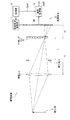
次に、図13および図14を参照して、本実施の形態の撮像装置1の特徴的な作用について、比較例と比較しつつ詳細に説明する。ここで、図13および図14は、比較例に係る撮像装置(撮像装置1におけるマイクロレンズアレイ12の代わりに、各マイクロレンズ12−1のピッチp12が前述の(1)式を満たさないマイクロレンズアレイ102を設けたもの)において、像高ずれが生ずる場合(像高ずれ量Δ>0の場合)の撮像の様子を表したものである。
Next, with reference to FIG. 13 and FIG. 14, the characteristic operation of the imaging device 1 of the present embodiment will be described in detail in comparison with a comparative example. Here, FIG. 13 and FIG. 14 show an imaging apparatus according to a comparative example (in place of the
まず、例えば図13に示したように、メインレンズである撮像レンズ11の開口絞り10の位置が撮像レンズ11の主点P0からある程度離れている場合において、マイクロレンズアレイ12への入射光の主光線L0が光軸に対してある程度傾いているとき(撮像レンズ11の主点P0上に主光線L0がないとき)、開口絞り10の位置に依存して、各マイクロレンズ12−1の形状(円形状)に応じて撮像素子13上に結像する像(ユニット像)のピッチが、図中の矢印で示したように、符号P1の位置から符号P2の位置へとシフトする。
First, as shown in FIG. 13, for example, when the position of the
これにより、例えば図14に示したように、撮像素子13の受光面(マイクロレンズアレイ12側の面)において、像高ずれ量Δ(点Pdと点Peとの間の距離)による像高ずれが発生する。この像高ずれ量Δは、光軸と主光線L0との間の傾斜角をθ、主光線L0がマイクロレンズアレイ102上に結像する像高(点Pbと点Pfとの間の距離))をy、開口絞り10とマイクロレンズアレイ12との間の距離(点Paと点Pbとの間の距離)をL、マイクロレンズアレイ12の焦点距離(点Pbと点Pcとの間の距離)をf2とすると、以下の(14)式および(15)式により表される。また、マイクロレンズアレイ12上での像高yと、撮像素子13上に結像するユニット像の像高(点Pcと点Peとの間の距離)との比率は、以下の(16)式により表される。
tanθ=(y/L)=(Δ/f2) …(14)
Δ={(y×f2)/L} …(15)
(y+Δ)/y=(L+f2)/L …(16)
As a result, for example, as shown in FIG. 14, the image height shift due to the image height shift amount Δ (the distance between the point Pd and the point Pe) on the light receiving surface (the surface on the
tan θ = (y / L) = (Δ / f2) (14)
Δ = {(y × f2) / L} (15)
(Y + Δ) / y = (L + f2) / L (16)
このようにして、図13および図14に示した比較例に係る撮像装置では、マイクロレンズアレイ102において、各マイクロレンズ12−1のピッチp12が、前述の(11)式を満たしていないため、上記(14)式および(15)式で表される像高ずれ量Δによる像高ずれが発生してしまっている。言い換えると、前述したように、撮像素子13により得られる撮像データD0が、光の強度分布に加えてその光の進行方向の情報を含んでいる場合であっても、各マイクロレンズ12−1のピッチp12が撮像素子13の画素Pの整数倍になっていないため、各マイクロレンズ12−1において一方向に割り当てられる画素Pの画素数が変動し、画像処理部14において、リフォーカス画像や任意視点画像等の再構築画像が得られなくなってしまう場合がある。
Thus, in the imaging device according to the comparative example illustrated in FIGS. 13 and 14, in the
これに対し、本実施の形態の撮像装置1では、マイクロレンズアレイ12において、各マイクロレンズ12−1のピッチp12が、前述の(11)式を満たすようになっている。これにより、上記比較例に係る像高補正係数(上記(16)式の逆数に対応する)の値が常に「1」となるため、撮像素子13により得られる撮像データD0において、撮像素子13の受光面(マイクロレンズアレイ12側の面)における像高ずれ(像高ずれ量Δによる像高ずれ)の発生が回避される。
On the other hand, in the imaging device 1 of the present embodiment, in the
以上のように本実施の形態では、各マイクロレンズ12−1のピッチp12が上記(11)式を満たすようにしたので、撮像素子13により得られる撮像データD0において、撮像素子13の受光面における像高ずれの発生を回避することができる。よって、そのような撮像データD0を用いて画像処理部14により再構築画像を生成するようにすれば、光の進行方向の情報を含むようにして撮像データを取得する場合において、適切な再構築画像の生成を可能とすることができる。
As described above, in the present embodiment, the pitch p12 of each microlens 12-1 satisfies the above expression (11). Therefore, in the imaging data D0 obtained by the
また、以下説明する第2の実施の形態のように、像高補正を行う像高補正部(後述する像高補正部149)を設ける必要がなく、各マイクロレンズ12−1のピッチp12の設定のみによって実現することができるため、マイクロレンズアレイ12のピッチ設計時に想定した開口絞り10の位置が変位しない限り、簡易に適切な再構築画像の生成を可能とすることができる。
Further, unlike the second embodiment described below, it is not necessary to provide an image height correction unit (image
[第2の実施の形態]
次に、本発明の第2の実施の形態について説明する。本実施の形態の撮像装置は、第1の実施の形態の撮像装置1において、画像処理部14の代わりに以下説明する画像処理部14Aを設けると共に、マイクロレンズアレイ12の代わりに、各マイクロレンズ12−1のピッチp12が前述の(1)式を満たさないマイクロレンズアレイ(前述のマイクロレンズアレイ102に対応)を設けるようにしたものである。なお、第1の実施の形態における構成要素と同一のものには同一の符号を付し、適宜説明を省略する。
[Second Embodiment]
Next, a second embodiment of the present invention will be described. The imaging apparatus of the present embodiment is provided with an image processing unit 14A described below instead of the
図15は、本実施の形態に係る撮像装置に用いられる画像処理部(画像処理部14A)の機能ブロック構成を表すものである。この画像処理部14Aは、第1の実施の形態で説明した画像処理部14において、補間処理部143と並び替え処理部144との間に、像高補正部149を設けるようにしたものである。
FIG. 15 illustrates a functional block configuration of an image processing unit (image processing unit 14A) used in the imaging apparatus according to the present embodiment. The image processing unit 14A is configured such that an image
像高補正部149は、各マイクロレンズ12−1に対応して撮像素子13上に結像する像(ユニット像)の一辺方向の大きさ(各マイクロレンズ12−1のピッチp12に対応する)が、撮像素子13の画素Pにおける一辺方向の画素サイズsの整数倍となるように、撮像素子13により得られた撮像データ(具体的には、補間処理部143による補間処理後の撮像データD1)に対して像高補正を行うことにより、像高補正後の撮像データD3を生成し、この撮像データD3を並び替え処理部144へと供給するものである。具体的には、この像高補正部149は、撮像データD1に対し、以下の(17)式および(18)式で表される補正係数kを用いて像高補正を行う(撮像データD1に対して補正係数kを乗ずることにより、撮像データD3を生成する)ようになっている。なお、β=1のときは、(18)式により、p12=m×sとなる。
k=β×{L/(L+f2)} …(17)
β=(m×s)/p12 …(18)
The image
k = β × {L / (L + f2)} (17)
β = (m × s) / p12 (18)
このような構成により本実施の形態では、像高補正部149によって、マイクロレンズ12−1に対応して撮像素子13上に結像する像(ユニット像)の一辺方向の大きさ(各マイクロレンズ12−1のピッチp12に対応する)が、画素Pにおける一辺方向の画素サイズsの整数倍となるように、撮像データD1に対して像高補正がなされるため、そのような像高補正後の撮像データD3において、開口絞り10の位置((開口絞り10とマイクロレンズアレイ12との間の距離L)によらず、撮像素子13の受光面(マイクロレンズアレイ12側の面)における像高ずれ(像高ずれ量Δによる像高ずれ)が生じなくなる。よって、この像高補正後の撮像データD3を用いて画像処理部14Aにより再構築画像を生成するようにすれば、上記第1の実施の形態と同様に、光の進行方向の情報を含むようにして撮像データを取得する場合において、メインレンズ(撮像レンズ11)の開口絞り10の位置によらずに適切な再構築画像の生成を可能とすることができる。
With this configuration, in the present embodiment, the image
以上、第1および第2の実施の形態を挙げて本発明を説明したが、本発明はこれらの実施の形態に限定されるものではなく、種々の変形が可能である。 Although the present invention has been described with reference to the first and second embodiments, the present invention is not limited to these embodiments, and various modifications can be made.
例えば、上記第1の実施の形態では、各マイクロレンズ12−1のピッチp12が上記(11)式を満たすようにした場合について説明する一方、上記第2の実施の形態では、像高補正部149により像高補正を行う場合について説明したが、例えば、これら第1および第2の実施の形態において説明した構成を両方とも兼ね備えるようにしてもよい。すなわち、各マイクロレンズ12−1のピッチp12が上記(11)式を満たすようにすると共に、像高補正部149により像高補正を行うようにしてもよい。
For example, in the first embodiment, the case where the pitch p12 of each microlens 12-1 satisfies the above expression (11) will be described, while in the second embodiment, the image height correction unit. Although the case where the image height correction is performed according to 149 has been described, for example, both of the configurations described in the first and second embodiments may be provided. That is, the pitch p12 of each microlens 12-1 may satisfy the above expression (11), and the image
また、上記実施の形態では、画像処理部14,14Aを、撮像装置の構成要素の一つとして説明したが、必ずしもこの画像処理部が撮像装置の内部に設けられている必要はない。具体的には、画像処理部を、撮像装置とは別の装置、例えばPC(Personal Computer:パーソナルコンピュータ)などに設けておき、撮像装置で得られた撮像データをPCへ転送し、PCにおいて画像処理を施すようにすることも可能である。
In the above-described embodiment, the
また、上記実施の形態では、開口絞り10の位置を撮像レンズの像側(出射側)に配置した構成としているが、これに限定されず、撮像レンズの被写体側(入射側)あるいは、撮像レンズ内部に設けられた構成であってもよい。
In the above embodiment, the position of the
また、上記実施の形態では、カラーフィルタの一例として、赤(R)、緑(G)および青(B)の3原色のカラーフィルタがR:G:B=1:2:1の比率で市松状に配置されたBayer配列のカラーフィルタ(原色フィルタ)を挙げて説明したが、他の配列のカラーフィルタを用いるようにしてもよい。例えば、黄(Y)、マゼンダ(M)、シアン(C)および緑(G)の4補色のカラーフィルタ(黄色カラーフィルタ、マゼンダカラーフィルタ、シアンカラーフィルタおよび緑色カラーフィルタ)がY:M:C:G=1:1:1:1の比率で市松状に配置されたカラーフィルタ(補色フィルタ)を用いるようにしてもよい。 In the above embodiment, as an example of the color filter, the color filters of the three primary colors of red (R), green (G), and blue (B) are checked at a ratio of R: G: B = 1: 2: 1. In the above description, the Bayer array color filters (primary color filters) arranged in the shape are described. However, other array color filters may be used. For example, yellow (Y), magenta (M), cyan (C) and green (G) four complementary color filters (yellow color filter, magenta color filter, cyan color filter and green color filter) are Y: M: C. : Color filters (complementary color filters) arranged in a checkered pattern at a ratio of G = 1: 1: 1: 1: 1 may be used.
また、上記実施の形態では、撮像データ内の画素データの補間処理の一例としてデモザイク処理を挙げて説明したが、他の補間処理を行うようにしてもよい。 In the above-described embodiment, the demosaic process has been described as an example of the interpolation process of the pixel data in the imaging data. However, other interpolation processes may be performed.
さらに、上記実施の形態では、画像処理部14において行われる並び替え処理を含む画像処理の一例として、「Light Field Photography」を利用したリフォーカス演算処理について説明したが、そのような並び替え処理を含む画像処理としてはこれには限られず、例えば、焦点ぼかし処理や被写体深度調整処理などに対して適用するようにしてもよい。
Furthermore, in the above-described embodiment, the refocus calculation process using “Light Field Photography” has been described as an example of the image process including the rearrangement process performed in the
1…撮像装置、10…開口絞り、10A…開口部、11…撮像レンズ、110…撮像レンズ面、12…マイクロレンズアレイ、12−1…マイクロレンズ、120,120A,120B…リフォーカス面、13…撮像素子、13D…再構築画素領域、13−1…受光領域、130…撮像面、14,14A…画像処理部、141…欠陥補正部、142…クランプ処理部、143…補間処理部、144…並び替え処理部、145…ノイズ低減部、146…輪郭強調部、147…ホワイトバランス調整部、148…ガンマ補正部、149…像高補正部、15…撮像素子駆動部、16…制御部、17,17R,17G,17B…カラーフィルタ、2…撮像対象物(被写体)、f1,f2…焦点距離、L…開口絞りとマイクロレンズアレイとの間の距離、P…画素、P0…主点、p12…マイクロレンズのピッチ、s…画素の一辺の画素サイズ、y…像高、Δ…像高ずれ量、D0,D1,D10,D2,D3,Dout…撮像データ、Sout…制御信号、L0…主光線。 DESCRIPTION OF SYMBOLS 1 ... Imaging device, 10 ... Aperture stop, 10A ... Aperture, 11 ... Imaging lens, 110 ... Imaging lens surface, 12 ... Micro lens array, 12-1 ... Micro lens, 120, 120A, 120B ... Refocus surface, 13 ... Image sensor, 13D ... Reconstructed pixel area, 13-1 ... Light receiving area, 130 ... Imaging surface, 14, 14A ... Image processor, 141 ... Defect corrector, 142 ... Clamp processor, 143 ... Interpolator, 144 ... rearrangement processing unit, 145 ... noise reduction unit, 146 ... contour enhancement unit, 147 ... white balance adjustment unit, 148 ... gamma correction unit, 149 ... image height correction unit, 15 ... image sensor driving unit, 16 ... control unit, 17, 17R, 17G, 17B ... color filter, 2 ... imaging object (subject), f1, f2 ... focal length, L ... distance between aperture stop and microlens array P: Pixel, P0: Principal point, p12: Micro lens pitch, s: Pixel size of one side of the pixel, y: Image height, Δ: Image height deviation amount, D0, D1, D10, D2, D3, Dout ... Imaging Data, Sout ... control signal, L0 ... chief ray.
Claims (4)
受光した光に基づいて撮像データを取得する撮像素子と、
前記撮像レンズ部と前記撮像素子との間で撮像レンズ部の焦点面上に配置されると共に、前記撮像素子の複数の撮像画素に対して1つのマイクロレンズが対応するように配列された複数のマイクロレンズを有するマイクロレンズアレイ部とを備え、
以下の(1)式を満たす
撮像装置。
p=(m×s)×{L/(L+f)} …(1)
但し、
p:マイクロレンズ間のピッチ
s:前記撮像画素における所定方向の画素サイズ
m:各マイクロレンズにおいて前記所定方向に割り当てられる撮像画素の画素数(整数)
L:前記開口絞りと前記マイクロレンズアレイ部との間の距離
f:各マイクロレンズの焦点距離 An imaging lens unit having an aperture stop;
An image sensor that acquires imaging data based on the received light;
A plurality of microlenses arranged on the focal plane of the imaging lens unit between the imaging lens unit and the imaging element and arranged so as to correspond to a plurality of imaging pixels of the imaging element A microlens array section having a microlens,
An imaging device that satisfies the following expression (1).
p = (m × s) × {L / (L + f)} (1)
However,
p: pitch between micro lenses s: pixel size in a predetermined direction in the imaging pixels m: number of imaging pixels (integer) assigned in the predetermined direction in each micro lens
L: distance between the aperture stop and the microlens array section f: focal length of each microlens
請求項1に記載の撮像装置。 The imaging apparatus according to claim 1, further comprising an image processing unit configured to perform predetermined image processing on imaging data obtained from the imaging element.
受光した光に基づいて撮像データを取得する撮像素子と、
前記撮像レンズ部と前記撮像素子との間で撮像レンズ部の焦点面上に配置されると共に、前記撮像素子の複数の撮像画素に対して1つのマイクロレンズが対応するように配列された複数のマイクロレンズを有するマイクロレンズアレイ部と、
各マイクロレンズに対応して前記撮像素子上に結像する像の所定方向の大きさが、前記撮像画素における前記所定方向の画素サイズの整数倍となるように、前記撮像素子により得られた撮像データに対して像高補正を行う像高補正部と
を備え、
前記像高補正部は、前記撮像データに対し、以下の(2)式および(3)式で表される補正係数kを用いて像高補正を行う
撮像装置。
k=β×{L/(L+f)} …(2)
β=(m×s)/p …(3)
但し、
p:マイクロレンズ間のピッチ
s:前記撮像画素における前記所定方向の画素サイズ
m:各マイクロレンズにおいて前記所定方向に割り当てられる撮像画素の画素数(整数)
L:前記開口絞りと前記マイクロレンズアレイ部との間の距離
f:各マイクロレンズの焦点距離 An imaging lens unit having an aperture stop;
An image sensor that acquires imaging data based on the received light;
A plurality of microlenses arranged on the focal plane of the imaging lens unit between the imaging lens unit and the imaging element and arranged so as to correspond to a plurality of imaging pixels of the imaging element A microlens array section having a microlens;
Imaging obtained by the imaging device so that the size in the predetermined direction of the image formed on the imaging device corresponding to each microlens is an integral multiple of the pixel size of the imaging pixel in the predetermined direction. An image height correction unit that performs image height correction on the data ,
The image height correction unit performs image height correction on the imaging data using a correction coefficient k expressed by the following equations (2) and (3) .
k = β × {L / (L + f)} (2)
β = (m × s) / p (3)
However,
p: pitch between microlenses
s: pixel size in the predetermined direction in the imaging pixel
m: Number of imaging pixels (integer) assigned in the predetermined direction in each microlens
L: Distance between the aperture stop and the microlens array part
f: Focal length of each microlens
請求項3に記載の撮像装置。 The imaging apparatus according to claim 3, further comprising an image processing unit configured to perform predetermined image processing on imaging data after the image height correction by the image height correction unit.
Priority Applications (4)
| Application Number | Priority Date | Filing Date | Title |
|---|---|---|---|
| JP2008016716A JP4941332B2 (en) | 2008-01-28 | 2008-01-28 | Imaging device |
| US12/318,639 US8102459B2 (en) | 2008-01-28 | 2009-01-05 | Image pickup apparatus |
| CN2009100098583A CN101500086B (en) | 2008-01-28 | 2009-01-24 | Image pickup apparatus |
| EP09151492A EP2083446B1 (en) | 2008-01-28 | 2009-01-28 | Image pickup apparatus |
Applications Claiming Priority (1)
| Application Number | Priority Date | Filing Date | Title |
|---|---|---|---|
| JP2008016716A JP4941332B2 (en) | 2008-01-28 | 2008-01-28 | Imaging device |
Publications (3)
| Publication Number | Publication Date |
|---|---|
| JP2009177727A JP2009177727A (en) | 2009-08-06 |
| JP2009177727A5 JP2009177727A5 (en) | 2010-05-06 |
| JP4941332B2 true JP4941332B2 (en) | 2012-05-30 |
Family
ID=40578630
Family Applications (1)
| Application Number | Title | Priority Date | Filing Date |
|---|---|---|---|
| JP2008016716A Expired - Fee Related JP4941332B2 (en) | 2008-01-28 | 2008-01-28 | Imaging device |
Country Status (4)
| Country | Link |
|---|---|
| US (1) | US8102459B2 (en) |
| EP (1) | EP2083446B1 (en) |
| JP (1) | JP4941332B2 (en) |
| CN (1) | CN101500086B (en) |
Families Citing this family (50)
| Publication number | Priority date | Publication date | Assignee | Title |
|---|---|---|---|---|
| JP4826152B2 (en) * | 2005-06-23 | 2011-11-30 | 株式会社ニコン | Image composition method and imaging apparatus |
| US10298834B2 (en) | 2006-12-01 | 2019-05-21 | Google Llc | Video refocusing |
| US8289440B2 (en) * | 2008-12-08 | 2012-10-16 | Lytro, Inc. | Light field data acquisition devices, and methods of using and manufacturing same |
| JP4706882B2 (en) * | 2009-02-05 | 2011-06-22 | ソニー株式会社 | Imaging device |
| DE102010031535A1 (en) | 2010-07-19 | 2012-01-19 | Fraunhofer-Gesellschaft zur Förderung der angewandten Forschung e.V. | An image pickup device and method for picking up an image |
| JP5593913B2 (en) * | 2010-07-22 | 2014-09-24 | カシオ計算機株式会社 | Image generating apparatus, image generating program, and image generating method |
| JP5214754B2 (en) * | 2011-02-25 | 2013-06-19 | 株式会社東芝 | Solid-state imaging device and portable information terminal |
| JP5623313B2 (en) * | 2011-03-10 | 2014-11-12 | キヤノン株式会社 | Imaging apparatus and imaging optical system |
| JP6080417B2 (en) * | 2011-08-19 | 2017-02-15 | キヤノン株式会社 | Image processing apparatus and image processing method |
| JP5618943B2 (en) * | 2011-08-19 | 2014-11-05 | キヤノン株式会社 | Image processing method, imaging apparatus, image processing apparatus, and image processing program |
| JP2013081087A (en) * | 2011-10-04 | 2013-05-02 | Sony Corp | Imaging device |
| JP5854984B2 (en) * | 2012-02-20 | 2016-02-09 | キヤノン株式会社 | Image processing apparatus, imaging apparatus, control method, and program |
| CN103297677B (en) * | 2012-02-24 | 2016-07-06 | 卡西欧计算机株式会社 | Generate video generation device and the image generating method of reconstruct image |
| US8948545B2 (en) | 2012-02-28 | 2015-02-03 | Lytro, Inc. | Compensating for sensor saturation and microlens modulation during light-field image processing |
| US8995785B2 (en) | 2012-02-28 | 2015-03-31 | Lytro, Inc. | Light-field processing and analysis, camera control, and user interfaces and interaction on light-field capture devices |
| US8831377B2 (en) | 2012-02-28 | 2014-09-09 | Lytro, Inc. | Compensating for variation in microlens position during light-field image processing |
| US8811769B1 (en) | 2012-02-28 | 2014-08-19 | Lytro, Inc. | Extended depth of field and variable center of perspective in light-field processing |
| US9420276B2 (en) | 2012-02-28 | 2016-08-16 | Lytro, Inc. | Calibration of light-field camera geometry via robust fitting |
| JP2013198016A (en) * | 2012-03-21 | 2013-09-30 | Casio Comput Co Ltd | Imaging apparatus |
| KR20130112541A (en) * | 2012-04-04 | 2013-10-14 | 삼성전자주식회사 | Plenoptic camera apparatus |
| US9451147B2 (en) * | 2012-06-11 | 2016-09-20 | Canon Kabushiki Kaisha | Image processing apparatus, image processing method, image pickup apparatus, method of controlling image pickup apparatus, and non-transitory computer-readable storage medium |
| US9858649B2 (en) | 2015-09-30 | 2018-01-02 | Lytro, Inc. | Depth-based image blurring |
| JP5978082B2 (en) * | 2012-09-19 | 2016-08-24 | 日本放送協会 | Stereoscopic image capturing apparatus and method |
| JP6080541B2 (en) * | 2012-12-26 | 2017-02-15 | 日本放送協会 | Stereoscopic image acquisition apparatus and stereoscopic image acquisition method |
| US20140184861A1 (en) * | 2012-12-30 | 2014-07-03 | Todor Georgiev | Accurate plenoptic rendering with defocus blur |
| US10334151B2 (en) | 2013-04-22 | 2019-06-25 | Google Llc | Phase detection autofocus using subaperture images |
| US9525819B2 (en) * | 2014-03-07 | 2016-12-20 | Ricoh Company, Ltd. | Enhancing spatial resolution of images from light field imaging systems using sub-pixel disparity |
| US9438778B2 (en) | 2014-08-08 | 2016-09-06 | Industrial Technology Research Institute | Image pickup device and light field image pickup lens |
| US9635332B2 (en) | 2014-09-08 | 2017-04-25 | Lytro, Inc. | Saturated pixel recovery in light-field images |
| US10546424B2 (en) | 2015-04-15 | 2020-01-28 | Google Llc | Layered content delivery for virtual and augmented reality experiences |
| US10419737B2 (en) | 2015-04-15 | 2019-09-17 | Google Llc | Data structures and delivery methods for expediting virtual reality playback |
| US10341632B2 (en) | 2015-04-15 | 2019-07-02 | Google Llc. | Spatial random access enabled video system with a three-dimensional viewing volume |
| US10567464B2 (en) | 2015-04-15 | 2020-02-18 | Google Llc | Video compression with adaptive view-dependent lighting removal |
| US10540818B2 (en) | 2015-04-15 | 2020-01-21 | Google Llc | Stereo image generation and interactive playback |
| US10440407B2 (en) | 2017-05-09 | 2019-10-08 | Google Llc | Adaptive control for immersive experience delivery |
| US10444931B2 (en) | 2017-05-09 | 2019-10-15 | Google Llc | Vantage generation and interactive playback |
| US10275898B1 (en) | 2015-04-15 | 2019-04-30 | Google Llc | Wedge-based light-field video capture |
| US10412373B2 (en) | 2015-04-15 | 2019-09-10 | Google Llc | Image capture for virtual reality displays |
| US11328446B2 (en) | 2015-04-15 | 2022-05-10 | Google Llc | Combining light-field data with active depth data for depth map generation |
| US10469873B2 (en) | 2015-04-15 | 2019-11-05 | Google Llc | Encoding and decoding virtual reality video |
| US10565734B2 (en) | 2015-04-15 | 2020-02-18 | Google Llc | Video capture, processing, calibration, computational fiber artifact removal, and light-field pipeline |
| US9979909B2 (en) | 2015-07-24 | 2018-05-22 | Lytro, Inc. | Automatic lens flare detection and correction for light-field images |
| CN107347129B (en) * | 2016-05-05 | 2020-02-14 | 中强光电股份有限公司 | Light field camera |
| US10275892B2 (en) | 2016-06-09 | 2019-04-30 | Google Llc | Multi-view scene segmentation and propagation |
| US10679361B2 (en) | 2016-12-05 | 2020-06-09 | Google Llc | Multi-view rotoscope contour propagation |
| US10594945B2 (en) | 2017-04-03 | 2020-03-17 | Google Llc | Generating dolly zoom effect using light field image data |
| US10474227B2 (en) | 2017-05-09 | 2019-11-12 | Google Llc | Generation of virtual reality with 6 degrees of freedom from limited viewer data |
| US10354399B2 (en) | 2017-05-25 | 2019-07-16 | Google Llc | Multi-view back-projection to a light-field |
| US10545215B2 (en) | 2017-09-13 | 2020-01-28 | Google Llc | 4D camera tracking and optical stabilization |
| US10965862B2 (en) | 2018-01-18 | 2021-03-30 | Google Llc | Multi-camera navigation interface |
Family Cites Families (14)
| Publication number | Priority date | Publication date | Assignee | Title |
|---|---|---|---|---|
| JP2600250B2 (en) * | 1988-02-22 | 1997-04-16 | ソニー株式会社 | Solid-state imaging device and video camera |
| JP3170847B2 (en) * | 1992-02-14 | 2001-05-28 | キヤノン株式会社 | Solid-state image sensor and optical device using the same |
| US6137535A (en) * | 1996-11-04 | 2000-10-24 | Eastman Kodak Company | Compact digital camera with segmented fields of view |
| JP4054094B2 (en) * | 1996-12-27 | 2008-02-27 | オリンパス株式会社 | Electronic endoscope |
| JP2005267457A (en) * | 2004-03-19 | 2005-09-29 | Casio Comput Co Ltd | Image processing device, imaging apparatus, image processing method and program |
| JP4672461B2 (en) | 2004-06-28 | 2011-04-20 | 株式会社バンダイナムコゲームス | Image generating apparatus, electronic device, printed material, image generating method and program |
| KR101134208B1 (en) | 2004-10-01 | 2012-04-09 | 더 보드 어브 트러스티스 어브 더 리랜드 스탠포드 주니어 유니버시티 | Imaging arrangements and methods therefor |
| CN101426085B (en) * | 2004-10-01 | 2012-10-03 | 小利兰·斯坦福大学托管委员会 | Imaging arrangements and methods therefor |
| JP4826152B2 (en) | 2005-06-23 | 2011-11-30 | 株式会社ニコン | Image composition method and imaging apparatus |
| US7723662B2 (en) | 2005-10-07 | 2010-05-25 | The Board Of Trustees Of The Leland Stanford Junior University | Microscopy arrangements and approaches |
| US7620309B2 (en) | 2006-04-04 | 2009-11-17 | Adobe Systems, Incorporated | Plenoptic camera |
| JP4802864B2 (en) * | 2006-05-29 | 2011-10-26 | 株式会社ニコン | Focus detection apparatus and imaging apparatus |
| JP5117691B2 (en) | 2006-07-07 | 2013-01-16 | 新日本無線株式会社 | Lead frame and method of manufacturing semiconductor device using the same |
| US20080173791A1 (en) * | 2007-01-19 | 2008-07-24 | Palum Russell J | Image sensor with three sets of microlenses |
-
2008
- 2008-01-28 JP JP2008016716A patent/JP4941332B2/en not_active Expired - Fee Related
-
2009
- 2009-01-05 US US12/318,639 patent/US8102459B2/en not_active Expired - Fee Related
- 2009-01-24 CN CN2009100098583A patent/CN101500086B/en not_active Expired - Fee Related
- 2009-01-28 EP EP09151492A patent/EP2083446B1/en not_active Expired - Fee Related
Also Published As
| Publication number | Publication date |
|---|---|
| CN101500086B (en) | 2011-07-06 |
| US20090190024A1 (en) | 2009-07-30 |
| CN101500086A (en) | 2009-08-05 |
| JP2009177727A (en) | 2009-08-06 |
| EP2083446A2 (en) | 2009-07-29 |
| EP2083446B1 (en) | 2012-08-01 |
| US8102459B2 (en) | 2012-01-24 |
| EP2083446A3 (en) | 2011-03-02 |
Similar Documents
| Publication | Publication Date | Title |
|---|---|---|
| JP4941332B2 (en) | Imaging device | |
| JP4483951B2 (en) | Imaging device | |
| JP5463718B2 (en) | Imaging device | |
| JP4905326B2 (en) | Imaging device | |
| JP5472584B2 (en) | Imaging device | |
| JP4967873B2 (en) | Imaging device | |
| JP4706882B2 (en) | Imaging device | |
| JP5067154B2 (en) | Imaging device | |
| US9826139B2 (en) | Image processing apparatus, image processing method, program, and image pickup apparatus having the image processing apparatus | |
| JP5676962B2 (en) | Focus detection apparatus and imaging apparatus | |
| JP2010057067A (en) | Image pickup apparatus and image processing apparatus | |
| JP4968527B2 (en) | Imaging device | |
| EP2630788A1 (en) | System and method for imaging using multi aperture camera | |
| US10674074B2 (en) | Image processing apparatus, image pickup apparatus, image processing method, and non-transitory computer-readable storage medium for generating an image based on a plurality of parallax images | |
| TW201143384A (en) | Camera module, image processing apparatus, and image recording method | |
| JP2009290268A (en) | Imaging apparatus | |
| JP6045208B2 (en) | Imaging device | |
| JP2015185943A (en) | Microlens with filter array and solid state image sensor | |
| JP6190119B2 (en) | Image processing apparatus, imaging apparatus, control method, and program | |
| WO2017170392A1 (en) | Optical device | |
| JP6929511B2 (en) | Image sensor and image sensor | |
| US9386207B2 (en) | Image-capturing apparatus | |
| JP5649702B2 (en) | Imaging device |
Legal Events
| Date | Code | Title | Description |
|---|---|---|---|
| A521 | Request for written amendment filed |
Free format text: JAPANESE INTERMEDIATE CODE: A523 Effective date: 20100317 |
|
| A621 | Written request for application examination |
Free format text: JAPANESE INTERMEDIATE CODE: A621 Effective date: 20100317 |
|
| A977 | Report on retrieval |
Free format text: JAPANESE INTERMEDIATE CODE: A971007 Effective date: 20110916 |
|
| A131 | Notification of reasons for refusal |
Free format text: JAPANESE INTERMEDIATE CODE: A131 Effective date: 20110922 |
|
| A521 | Request for written amendment filed |
Free format text: JAPANESE INTERMEDIATE CODE: A523 Effective date: 20111017 |
|
| TRDD | Decision of grant or rejection written | ||
| A01 | Written decision to grant a patent or to grant a registration (utility model) |
Free format text: JAPANESE INTERMEDIATE CODE: A01 Effective date: 20120131 |
|
| A01 | Written decision to grant a patent or to grant a registration (utility model) |
Free format text: JAPANESE INTERMEDIATE CODE: A01 |
|
| A61 | First payment of annual fees (during grant procedure) |
Free format text: JAPANESE INTERMEDIATE CODE: A61 Effective date: 20120213 |
|
| R151 | Written notification of patent or utility model registration |
Ref document number: 4941332 Country of ref document: JP Free format text: JAPANESE INTERMEDIATE CODE: R151 |
|
| FPAY | Renewal fee payment (event date is renewal date of database) |
Free format text: PAYMENT UNTIL: 20150309 Year of fee payment: 3 |
|
| R250 | Receipt of annual fees |
Free format text: JAPANESE INTERMEDIATE CODE: R250 |
|
| R250 | Receipt of annual fees |
Free format text: JAPANESE INTERMEDIATE CODE: R250 |
|
| R250 | Receipt of annual fees |
Free format text: JAPANESE INTERMEDIATE CODE: R250 |
|
| R250 | Receipt of annual fees |
Free format text: JAPANESE INTERMEDIATE CODE: R250 |
|
| R250 | Receipt of annual fees |
Free format text: JAPANESE INTERMEDIATE CODE: R250 |
|
| LAPS | Cancellation because of no payment of annual fees |